CodeWarrior Debugger - Welcome to Freescale - Freescale Semiconductor
Freescale SemiconductorData Sheet: Advance Information
Document Number: MPC5604PRev. 2, 11/2008
MPC5604P144 LQFP20 mm x 20 mm
100 LQFP14 mm x 14 mm
MPC5604P Microcontroller Data Sheet
• Single issue, 32-bit Power Architecture™ CPU core complex (e200z0h) with Harvard architecture
• Up to 512 KB on-chip code flash memory with ECC plus 64 KB on-chip data flash with ECC
• Up to 40 KB SRAM on-chip with ECC• Interrupt controller (INTC) capable of handling 144
selectable-priority interrupt sources• Up to two FMPLL modules• Clock Monitor Unit (CMU) to monitor the integrity
of the main crystal oscillator and the PLL and act as a frequency meter, measuring the frequency of one clock source and comparing it to a reference clock
• 16 MHz internal RC Oscillator (trimmable)• Periodic Interrupt Timer (PIT) includes four timer
channels with 32-bit counter resolution• Windowed software watchdog (SWT)• Output compare system timer (STM) to support
AUTOSAR task protection• Crossbar switch (XBAR) architecture for concurrent
access to peripherals, flash memory or RAM from multiple bus masters (AMBA 2.0 v6 AHB)
• 16-channel Enhanced Direct Memory Access (eDMA) controller with multiple transfer request sources using DMA MUX
• System Integration Unit (SIU) Lite; controls the GPIO mode of the pads, the pads alternate function, and the pads configuration
• Boot assist module (BAM) supports downloading operation to internal SRAM via serial link (FlexCAN or LINFlex or FlexRay)
• FlexPWM motor control PWM module (1 x 8 PWM channels)
• Two enhanced eTimer timer modules (six channels each) with dedicated motor control and quadrature decode features integrated
• Embedded junction temperature sensor
© Freescale Semiconductor, Inc., 2008. All rights reserved.
Preliminary—Subject to Change Without Notice
This document contains information on a product under developmright to change or discontinue this product without notice.
• Safety Port to support functional safety architectures on the ECU level. Can be optionally used as a second FlexCAN module with 32 message buffers.
• Two independent 10-bit analog-to-digital converters (ADCs) with a conversion time target of 700 ns for the analog section. Each converter supports 16 channels (ADC0: channel 15 dedicated to the Temperature sensor; ADC1: channel 15 for the internal 1.2 V rail; channels 11 to 14 shared between the two converters)
• FlexPWM to ADC and eTimer Cross Triggering Unit (CTU)
• Fault Collection Unit (FCU) for functional safety• Four Serial Peripheral Interface (DSPI) modules• Two Serial Communication Interface (LINFlex)
modules with LIN support• FlexCAN Controller Area Network module with 32
message buffers• Dual channel FlexRay™ Controller with 32 message
buffers (512 KB device only)• GPIO
— 144-pin package: 82 general-purpose pins supporting input/output operations plus 26 general-purpose pins supporting input operations (108 in total). Out of these 108 pins, 32 have external interrupt capability.
— 100-pin package: 51 general-purpose pins supporting input/output operations plus 16 general-purpose pins supporting input operations (67 in total). Out of these 67 pins, 25 have external interrupt capability.
• Nexus development interface (NDI) per IEEE-ISTO 5001-2003 standard Class 2+
• JTAG (IEEE 1149.1) 4-pin interface• Voltage regulator (VREG) for regulation into 3.3 V -
5 V input down to 1.2 V nominal core logic level with external transistor
ent. Freescale reserves the
MPC5604P Microcontroller Data Sheet, Rev. 2
Preliminary—Subject to Change Without Notice
Freescale Semiconductor2
Table of Contents1 Overview. . . . . . . . . . . . . . . . . . . . . . . . . . . . . . . . . . . . . . . . . .3
1.1 Device Comparison. . . . . . . . . . . . . . . . . . . . . . . . . . . . .31.2 Block Diagram. . . . . . . . . . . . . . . . . . . . . . . . . . . . . . . . .4
2 Package Pinouts and Signal Descriptions . . . . . . . . . . . . . . . .62.1 Package Pinouts . . . . . . . . . . . . . . . . . . . . . . . . . . . . . . .62.2 Pin Descriptions . . . . . . . . . . . . . . . . . . . . . . . . . . . . . . .8
2.2.1 Power Supply and Reference Voltage Pins . . . . .82.2.2 System Pins. . . . . . . . . . . . . . . . . . . . . . . . . . . . .92.2.3 Pin Muxing. . . . . . . . . . . . . . . . . . . . . . . . . . . . .10
3 Electrical characteristics . . . . . . . . . . . . . . . . . . . . . . . . . . . . .253.1 Absolute Maximum Ratings . . . . . . . . . . . . . . . . . . . . .253.2 Recommended Operating Conditions. . . . . . . . . . . . . .263.3 Thermal Characteristics . . . . . . . . . . . . . . . . . . . . . . . .28
3.3.1 General Notes for Specifications at MaximumJunction Temperature . . . . . . . . . . . . . . . . . . . .29
3.4 Electromagnetic Interference (EMI) Characteristics . . .313.5 Electrostatic Discharge (ESD) Characteristics . . . . . . .323.6 Voltage Regulator Electrical Characteristics . . . . . . . . .333.7 Power Up/Down Sequencing . . . . . . . . . . . . . . . . . . . .343.8 DC electrical Characteristics. . . . . . . . . . . . . . . . . . . . .34
3.8.1 NVUSRO Register . . . . . . . . . . . . . . . . . . . . . . .343.8.2 DC Electrical Characteristics (5 V) . . . . . . . . . .353.8.3 DC Electrical characteristics (3.3 V) . . . . . . . . .36
3.9 Temperature Sensor Electrical Characteristics . . . . . . .38
3.10 Main Oscillator Electrical Characteristics . . . . . . . . . . 383.11 FMPLL Electrical Characteristics. . . . . . . . . . . . . . . . . 393.12 16 MHz RC Oscillator Electrical Characteristics . . . . . 393.13 Analog-to-Digital Converter (ADC) Electrical
Characteristics. . . . . . . . . . . . . . . . . . . . . . . . . . . . . . . 413.13.1 Input Impedance and ADC Accuracy . . . . . . . . 413.13.2 ADC Input Leakage Current . . . . . . . . . . . . . . . 463.13.3 ADC Conversion Characteristics . . . . . . . . . . . 46
3.14 Flash Memory Electrical Characteristics . . . . . . . . . . . 483.15 AC Specifications. . . . . . . . . . . . . . . . . . . . . . . . . . . . . 49
3.15.1 Pad AC Specifications . . . . . . . . . . . . . . . . . . . 493.16 AC Timing Characteristics . . . . . . . . . . . . . . . . . . . . . . 51
3.16.1 Generic Timing Diagrams . . . . . . . . . . . . . . . . 513.16.2 RESET_B Pin Characteristics . . . . . . . . . . . . . 523.16.3 IEEE 1149.1 Interface Timing . . . . . . . . . . . . . 543.16.4 Nexus Timing . . . . . . . . . . . . . . . . . . . . . . . . . . 563.16.5 External Interrupt Timing (IRQ pin) . . . . . . . . . 583.16.6 DSPI Timing . . . . . . . . . . . . . . . . . . . . . . . . . . . 59
4 Package Characteristics . . . . . . . . . . . . . . . . . . . . . . . . . . . . 654.1 Package Mechanical Data . . . . . . . . . . . . . . . . . . . . . . 65
4.1.1 144 LQFP Mechanical Outline Drawing . . . . . . 654.1.2 100 LQFP Mechanical Outline Drawing . . . . . . 67
5 Ordering Information . . . . . . . . . . . . . . . . . . . . . . . . . . . . . . . 70

1 OverviewThis document provides electrical specifications, pin assignments, and package diagrams for the MPC5604P series of microcontroller units (MCUs). For functional characteristics, refer to the MPC5604P Microcontroller Reference Manual.
MPC5604P microcontrollers are members of a new family of next generation microcontrollers built on the Power Architecture™. This document describes the features of the family and options available within the family members, and highlights important electrical and physical characteristics of the devices.
The MPC5604P family of 32-bit microcontrollers is the latest achievement in integrated automotive application controllers. It belongs to an expanding range of automotive-focused products designed to address electrical hydraulic power steering (EHPS), electric power steering (EPS) and airbag applications. The advanced and cost-efficient host processor core of the MPC5604P automotive controller family complies with the Power Architecture embedded category, which is 100 percent user-mode compatible with the original PowerPC user instruction set architecture (UISA). It operates at speeds of up to 64 MHz and offers high performance processing optimized for low power consumption. It capitalizes on the available development infrastructure of current Power Architecture devices and is supported with software drivers, operating systems and configuration code to assist with users implementations.
1.1 Device ComparisonTable 1 provides a summary of different members of the MPC5604P family and their features to enable a comparison among the family members and an understanding of the range of functionality offered within this family.
Table 1. MPC5604P Device Comparison
Feature MPC5602P MPC5603P MPC5604P
Code flash memory (ECC) 256 KB 384 KB 512 KB
Data flash memory (ECC) 64 KB (4 × 16 KB blocks)
RAM (ECC) 20 KB 36 KB 40 KB
Processor core 32-bit e200z0h
Instruction set VLE
CPU performance 0 MHz - 64 MHz
FMPLL (frequency-modulated phase-locked loop) modules
1 2 2
INTC (interrupt controller) channels 100 144 144
PIT (periodic interrupt timer) 1 (includes 4 32-bit timers)
Enhanced DMA (direct memory access) channels
16
FlexRay — Yes1
FlexCAN (controller area network) 22,3
FCU (fault collection unit) Yes
CTU (cross triggering unit) Yes
eTimer channels 2 × 6
FlexPWM (pulse-width modulation) channels 8
Analog-to-digital converters (ADC) 2 10-bit ADCs26 (2 x13) channels on LQFP144 pkg16 (2 x8) channels on LQFP100 pkg
MPC5604P Microcontroller Data Sheet, Rev. 2
Preliminary—Subject to Change Without NoticeFreescale Semiconductor 3

1.2 Block DiagramFigure 1 shows a top-level block diagram of the MPC5604P MCU.
LINFlex modules 2
DSPI (deserial serial peripheral interface) modules
3 4
CRC (cyclic redundancy check) unit Yes
Junction temperature sensor Yes
JTAG interface Yes
Nexus port controller (NPC) Yes (Level 1+) Yes (Level 2+)
Supply Digital power supply4 3.3 V or 5 V single supply with external transistor
Analog power supply 3.3 V or 5 V
Internal RC oscillator 16 MHz
External crystal oscillator 4 MHz - 40 MHz
Packages 100 LQFP 100 LQFP144 LQFP
Temperature Standard ambient temperature -40 to 125 °C
Extended ambient temperature5 -40 to 145 °C
1 32 message buffers, dual-channel2 Each FlexCAN module has 32 message buffers3 One FlexCAN module can act as a Safety Port with a data rate of up to 7.5 MHz4 A given orderable part can be software-configured for either 3 V or 5 V operation.5 Thermally enhanced 100-pin and 144-pin LQFP packages are under analysis to support an extended ambient
temperature range of -40 to 145 °C. The packages are not yet available.
Table 1. MPC5604P Device Comparison (continued)
Feature MPC5602P MPC5603P MPC5604P
MPC5604P Microcontroller Data Sheet, Rev. 2
Preliminary—Subject to Change Without Notice Freescale Semiconductor4

Figure 1. MPC5604P Block Diagram
e200z0 Core
32-bitGeneralPurposeRegisters
SpecialPurposeRegisters
IntegerExecution
Unit
ExceptionHandler
VariableLength
EncodedInstructions
InstructionUnit
Load/StoreUnit
BranchPrediction
UnitJTAG
Nexus 2+
1.2 V RegulatorControl
XOSC
16 MHzRC-Oscillator
FMPLL_0(System)
FMPLL_1(FlexRay, MotCtrl)
Nexus PortController
InterruptController
FlexRayDMA2x16 channels
Master Master
Instruction32-bit
Master
Data32-bit
Master
512 KBCode Flash
ECC
64 KBData Flash
ECC
40 KBSRAMECC
SystemIntegrationUnit-Lite
BootAssist
Module
PIT
ST
M
SW
T
Slave Slave Slave
Crossbar Switch (XBAR, AMBA 2.0 v6 AHB)
Peripheral Bridge
Fle
xPW
M
CT
U
1.2
V R
ail V
reg
2×
4 ch.
11 4 11
Junc
. Tem
p. S
enso
r
2× 4× 2×
Fle
xCA
N
MC
M
Saf
ety
Por
t
Faul
t Col
lect
ion
Uni
t
N Controller Area Network (FlexCAN)PI Deserial Serial Peripheral InterfaceFlex Serial Communication Interface (LIN support)PLL Frequency-Modulated Phase-Locked LoopAM Static Random-Access MemoryxPWM Flexible Pulse Width Modulation
eTimer Enhanced TimerPIT Periodic Interrupt TimerSWT Software Watchdog TimerSTM System Timer Module
AD
C
eTim
er (
6ch)
DS
PI
LIN
Fle
x
MPC5604P Microcontroller Data Sheet, Rev. 2
Preliminary—Subject to Change Without NoticeFreescale Semiconductor 5

2 Package Pinouts and Signal Descriptions
2.1 Package PinoutsThe LQFP pinouts are shown in the following figures.
Figure 2. LQFP 144-pin Configuration (top view)1
1. Availability of port pin alternate functions depends on product selection
123456789101112131415161718192021222324252627282930313233343536
108107106105104103102101100999897969594939291908988878685848382818079787776757473
37 38 39 40 41 42 43 44 45 46 47 48 49 50 51 52 53 54 55 56 57 58 59 60 61 62 63 64 65 66 67 68 69 70 71 72
144
143
142
141
140
139
138
137
136
135
134
133
132
131
130
129
128
127
126
125
124
123
122
121
120
119
118
117
116
115
114
113
112
111
110
109
NMIdspi1 SCK/A[6]
flexray0 CA RX/etimer1 ETC[2]/ctu0 EXT TRG/D[1]nexus0 MDO[3]/F[4]nexus0 MDO[2]/F[5]
VDD_HV_IO0VSS_HV_IO0
nexus0 MDO[1]/F[6]nexus0 MDO 0
dspi1 SOUT/A[7]sscm DEBUG[4]/dspi0 CS0/flexpwm0 X[1]/C[4]
dspi1 SIN/A[8]sscm DEBUG[5]/dspi0 SCK/flexpwm0 FAULT[3]/C[5]
dspi1 CS0/etimer1 ETC[5]/dspi0 CS7/A[5]sscm DEBUG[7]/dspi0 SIN/flexpwm0 A[1]/C[7]
dspi0 CS1/etimer1 ETC[4]/lin1 TXD/C[3]VSS_LV_COR0VDD_LV_COR0
nexus0 MCKO/F[7]nexus0 MSEO1/F[8]
VDD_HV_IO1VSS_HV_IO1
nexus0 MSEO0/F[9]nexus0 EVTO/F[10]nexus0 EVTI/F[11]
flexpwm0 X[0]/lin1 TXD/D[9]VDD_HV_OSCVSS_HV_OSC
XTALEXTAL
RESET_Bdspi1 CS2/flexpwm0 FAULT[3]/dspi0 CS5/D[8]
dspi0 CS3/fcu0 F[0]/dspi3 SOUT/D[5]dspi0 CS2/dspi3 SCK/flexpwm0 FAULT[1]/D[6]
VSS_LV_PLLVDD_LV_PLL
A[4]/etimer1 ETC[0]/dspi2 CS1/etimer0 ETC[4]VPP TESTF[12]/etimer1 ETC[3]D[14]/flexpwm0 B[1]/dspi3 CS3/dspi3 SING[3]/flexpwm0 A[2]C[14]/etimer1 ETC[2]/ctu0 EXT TGRG[2]/flexpwm0 X[2]C[13]/etimer1 ETC[1]/ctu0 EXT IN/flexpwm0 ext. syncG[4]/flexpwm0 B[2]D[12]/flexpwm0 X[1]/lin1 RXDG[6]/flexpwm0 A[3]VDD_HV_FLVSS_HV_FLD[13]/flexpwm0 A[1]/dspi3 CS2/dspi3 SOUTVSS_LV_COR1VDD_LV_COR1A[3]/etimer0 ETC[3]/dspi2 CS0/flexpwm0 B[3]VDD_HV_IO2VSS_HV_IO2B[4]/jtag0 TDOjtag0 TCKjtag0 TMSB[5]/jtag0 TDIG[5]/flexpwm0 X[3]A[2]/etimer0 ETC[2]/dspi2 SIN/flexpwm0 A[3]G[7]/flexpwm0 B[3]C[12]/etimer0 ETC[5]/dspi2 CS3/dspi3 CS1G[8]/flexpwm0 FAULT[0]C[11]/etimer0 ETC[4]/dspi2 CS2/dspi3 CS0G[9]/flexpwm0 FAULT[1]D[11]/flexpwm0 B[0]/dspi3 CS1/dspi3 SCKG[10]/flexpwm0 FAULT[2]D[10]/flexpwm0 A[0]/dspi3 CS0G[11]/flexpwm0 FAULT[3]A[1]/etimer0 ETC[1]/dspi2 SOUT/fcu0 F[1]/DEBUG[7]A[0]/etimer0 ETC[0]/dspi2 SCK/fcu0 F[0]
dspi
1 C
S3/
fcu0
F[1
]/dsp
i3 S
IN/d
spi0
CS
4/D
[7]
fcu0
F[0
]/G[0
]ad
c0 A
N[4
]/E[1
]ad
c0 A
N[6
]/E[3
]ad
c0 A
N[2
]/C[1
]ad
c0 A
N[7
]/E[4
]ad
c0 A
N[0
]/lin
0 R
XD
/B[7
]ad
c0 A
N[8
]/E[5
]ad
c0 A
N[3
]/C[2
]ad
c0 A
N[9
]/E[6
]ad
c0 A
N[1
]/etim
er0
ET
C[5
]/B[8
]ad
c0 A
N[1
0]/E
[7]
adc0
AN
[5]/E
[2]
VD
D_H
V_A
D0
VS
S_H
V_A
D0
adc0
-adc
1 A
N[1
1]/B
[9]
adc0
-adc
1 A
N[1
2]/B
[10]
adc0
-adc
1 A
N[1
3]/B
[11]
adc0
-adc
1 A
N[1
4]/B
[12]
VD
D_H
V_A
D1
VS
S_H
V_A
D1
adc1
AN
[4]/D
[15]
adc1
AN
[6]/E
[8]
adc1
AN
[0]/l
in1
RX
D/B
[13]
adc1
AN
[7]/E
[9]
adc1
AN
[2]/B
[15]
adc1
AN
[8]/E
[10]
adc1
AN
[1]/e
timer
0 E
TC
[4]/B
[14]
adc1
AN
[9]/E
[11]
adc1
AN
[3]/C
[0]
adc1
AN
[10]
/E[1
2]ad
c1 A
N[5
]/E[0
]B
CT
RL
VD
D_L
V_R
EG
CO
RV
SS
_LV
_RE
GC
OR
VD
D_H
V_R
EG
A[1
5]/s
afet
ypor
t0 R
XD
/etim
er1
ET
C[5
]A
[14]
/saf
etyp
ort0
TX
D/e
timer
1 E
TC
[4]
C[6
]/ds
pi0
SO
UT
/flex
pwm
0 B
[1]/s
scm
DE
BU
G[6
]G
[1]/
fcu0
F[1
]D
[2]/
flexr
ay0
CB
RX
/etim
er1
ET
C[3
]/fle
xpw
m0
X[3
]F
[3]/
flexr
ay0
DB
G3/
dspi
3 C
S0
B[6
]/C
LKO
UT
/dsp
i2 C
S2
F[2
]/fle
xray
0 D
BG
2/ds
pi3
CS
1A
[13]
/dsp
i2 S
IN/fl
expw
m0
B[2
]/fle
xpw
m0
FAU
LT[0
]F
[1]/
flexr
ay0
DB
G1/
dspi
3 C
S2
A[9
]/ds
pi2
CS
1/fle
xpw
m0
FAU
LT[0
]/fle
xpw
m0
B[3
]F
[0]/
flexr
ay0
DB
G0/
dspi
3 C
S3
VS
S_L
V_C
OR
2V
DD
_LV
_CO
R2
C[8
]/ds
pi1
CS
1/fle
xpw
m0
FAU
LT[2
]/dsp
i0 C
S6
D[4
]/fle
xray
0 C
B T
R E
N/e
timer
1 E
TC
[5]/f
lexp
wm
0 B
[3]
D[3
]/fle
xray
0 C
B T
X/e
timer
1 E
TC
[4]/f
lexp
wm
0 A
[3]
VS
S_H
V_I
O3
VD
D_H
V_I
O3
D[0
]/fle
xray
0 C
A T
X/e
timer
1 E
TC
[1]/f
lexp
wm
0 B
[1]
C[1
5]/fl
exra
y0 C
A T
R E
N/e
timer
1 E
TC
[0]/f
lexp
wm
0 A
[1]/c
tu0
EX
T IN
/flex
pwm
0 ex
t. sy
ncC
[9]/
dspi
2 C
S3/
flexp
wm
0 FA
ULT
[2]/f
lexp
wm
0 X
[3]
A[1
2]/d
spi2
SO
UT
/flex
pwm
0 A
[2]/f
lexp
wm
0 B
[2]
E[1
5]/d
spi3
SIN
A[1
1]/d
spi2
SC
K/fl
expw
m0
A[0
]/fle
xpw
m0
A[2
]E
[14]
/dsp
i3 S
OU
TA
[10]
/dsp
i2 C
S0/
flexp
wm
0 B
[0]/f
lexp
wm
0 X
[2]
E[1
3]/d
spi3
SC
KB
[3]/
lin0
RX
D/s
scm
DE
BU
G[3
]F
[14]
/lin1
TX
DB
[2]/
lin0
TX
D/s
scm
DE
BU
G[2
]F
[15]
/lin1
RX
DF
[13]
/etim
er1
ET
C[4
]C
[10]
/dsp
i2 C
S2/
flexp
wm
0 FA
ULT
[1]/f
lexp
wm
0 A
[3]
B[1
]/ca
n0 R
XD
/etim
er1
ET
C[3
]/ssc
m D
EB
UG
[1]
B[0
]/ca
n0 T
XD
/etim
er1
ET
C[2
]/ssc
m D
EB
UG
[0]
144 LQFP
MPC5604P Microcontroller Data Sheet, Rev. 2
Preliminary—Subject to Change Without Notice Freescale Semiconductor6

Figure 3. LQFP 100-pin Configuration (top view)1
1. Availability of port pin alternate functions depends on product selection
12345678910111213141516171819202122232425
75747372717069686766656463626160595857565554535251
26 27 28 29 30 31 32 33 34 35 36 37 38 39 40 41 42 43 44 45 46 47 48 49 50
100 99 98 97 96 95 94 93 92 91 90 89 88 87 86 85 84 83 82 81 80 79 78 77 76
NMIdspi1 SCK/A[6]
flexray0 CA RX/etimer1 ETC[2]/ctu0 EXT TRG/D[1]dspi1 SOUT/A[7]
sscm DEBUG[4]/dspi0 CS0/flexpwm0 X[1]/C[4]dspi1 SIN/A[8]
sscm DEBUG[5]/dspi0 SCK/flexpwm0 FAULT[3]/C[5]dspi1 CS0/etimer1 ETC[5]/dspi0 CS7/A[5]
sscm DEBUG[7]/dspi0 SIN/flexpwm0 A[1]/C[7]dspi0 CS1/etimer1 ETC[4]/lin1 TXD/C[3]
VSS_LV_COR0VDD_LV_COR0
VDD_HV_IO1VSS_HV_IO1
flexpwm0 X[0]/lin1 TXD/D[9]VDD_HV_OSCVSS_HV_OSC
XTALEXTAL
RESET_Bdspi1 CS2/flexpwm0 FAULT[3]/dspi0 CS5/D[8]
dspi0 CS3/fcu0 F[0]/dspi3 SOUT/D[5]dspi0 CS2/dspi3 SCK/flexpwm0 FAULT[1]/D[6]
VSS_LV_PLLVDD_LV_PLL
A[4]/etimer1 ETC[0]/dspi2 CS1/etimer0 ETC[4]VPP TESTD[14]/flexpwm0 B[1]/dspi3 CS3/dspi3 SINC[14]/etimer1 ETC[2]/ctu0 EXT TGRC[13]/etimer1 ETC[1]/ctu0 EXT IN/flexpwm0 ext. syncD[12]/flexpwm0 X[1]/lin1 RXDVDD_HV_FLVSS_HV_FLD[13]/flexpwm0 A[1]/dspi3 CS2/dspi3 SOUTVSS_LV_COR1VDD_LV_COR1A[3]/etimer0 ETC[3]/dspi2 CS0/flexpwm0 B[3]VDD_HV_IO2VSS_HV_IO2B[4]/jtag0 TDOjtag0 TCKjtag0 TMSB[5]/jtag0 TDIA[2]/etimer0 ETC[2]/dspi2 SIN/flexpwm0 A[3]C[12]/etimer0 ETC[5]/dspi2 CS3/dspi3 CS1C[11]/etimer0 ETC[4]/dspi2 CS2/dspi3 CS0D[11]/flexpwm0 B[0]/dspi3 CS1/dspi3 SCKD[10]/flexpwm0 A[0]/dspi3 CS0A[1]/etimer0 ETC[1]/dspi2 SOUT/fcu0 F[1]/sscm DEBUG[7]A[0]/etimer0 ETC[0]/dspi2 SCK/fcu0 F[0]
dspi
1 C
S3/
fcu0
F[1
]/dsp
i3 S
IN/d
spi0
CS
4/D
[7]
adc0
AN
[4]/E
[1]
adc0
AN
[2]/C
[1]
adc0
AN
[0]/l
in0
RX
D/B
[7]
adc0
AN
[3]/C
[2]
adc0
AN
[1]/e
timer
0 E
TC
[5]/B
[8]
adc0
AN
[5]/E
[2]
VD
D_H
V_A
D0
VS
S_H
V_A
D0
adc0
-adc
1 A
N[1
1]/B
[9]
adc0
-adc
1 A
N[1
2]/B
[10]
adc0
-adc
1 A
N[1
3]/B
[11]
adc0
-adc
1 A
N[1
4]/B
[12]
VD
D_H
V_A
D1
VS
S_H
V_A
D1
adc1
AN
[4]/D
[15]
adc1
AN
[0]/l
in1
RX
D/B
[13]
adc1
AN
[2]/B
[15]
adc1
AN
[1]/e
timer
0 E
TC
[4]/B
[14]
adc1
AN
[3]/C
[0]
adc1
AN
[5]/E
[0]
BC
TR
LV
DD
_LV
_RE
GC
OR
VS
S_L
V_R
EG
CO
RV
DD
_HV
_RE
G
A[1
5]/s
afet
ypor
t0 R
XD
/etim
er1
ET
C[5
]A
[14]
/saf
etyp
ort0
TX
D/e
timer
1 E
TC
[4]
C[6
]/ds
pi0
SO
UT
/flex
pwm
0 B
[1]/s
scm
DE
BU
G[6
]D
[2]/
flexr
ay0
CB
RX
/etim
er1
ET
C[3
]/fle
xpw
m0
X[3
]B
[6]/
CLK
OU
T/d
spi2
CS
2A
[13]
/dsp
i2 S
IN/fl
expw
m0
B[2
]/fle
xpw
m0
FAU
LT[0
]A
[9]/
dspi
2 C
S1/
flexp
wm
0 FA
ULT
[0]/f
lexp
wm
0 B
[3]
VS
S_L
V_C
OR
2V
DD
_LV
_CO
R2
C[8
]/ds
pi1
CS
1/fle
xpw
m0
FAU
LT[2
]/dsp
i0 C
S6
D[4
]/fle
xray
0 C
B T
R E
N/e
timer
1 E
TC
[5]/f
lexp
wm
0 B
[3]
D[3
]/fle
xray
0 C
B T
X/e
timer
1 E
TC
[4]/f
lexp
wm
0 A
[3]
VS
S_H
V_I
O3
VD
D_H
V_I
O3
D[0
]/fle
xray
0 C
A T
X/e
timer
1 E
TC
[1]/f
lexp
wm
0 B
[1]
C[1
5]/fl
exra
y0 C
A T
R E
N/e
timer
1 E
TC
[0]/f
lexp
wm
0 A
[1]/c
tu0
EX
T IN
/flex
pwm
0 ex
t. sy
ncC
[9]/
dspi
2 C
S3/
flexp
wm
0 FA
ULT
[2]/f
lexp
wm
0 X
[3]
A[1
2]/d
spi2
SO
UT
/flex
pwm
0 A
[2]/f
lexp
wm
0 B
[2]
A[1
1]/d
spi2
SC
K/fl
expw
m0
A[0
]/fle
xpw
m0
A[2
]A
[10]
/dsp
i2 C
S0/
flexp
wm
0 B
[0]/f
lexp
wm
0 X
[2]
B[3
]/lin
0 R
XD
/ssc
m D
EB
UG
[3]
B[2
]/lin
0 T
XD
/ssc
m D
EB
UG
[2]
C[1
0]/d
spi2
CS
2/fle
xpw
m0
FAU
LT[1
]/fle
xpw
m0
A[3
]B
[1]/
can0
RX
D/e
timer
1 E
TC
[3]/s
scm
DE
BU
G[1
]B
[0]/
can0
TX
D/e
timer
1 E
TC
[2]/s
scm
DE
BU
G[0
]
100 LQFP
MPC5604P Microcontroller Data Sheet, Rev. 2
Preliminary—Subject to Change Without NoticeFreescale Semiconductor 7
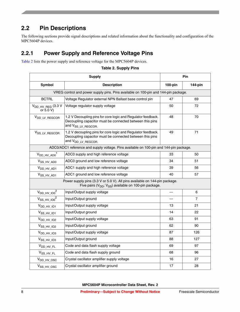
2.2 Pin DescriptionsThe following sections provide signal descriptions and related information about the functionality and configuration of the MPC5604P devices.
2.2.1 Power Supply and Reference Voltage PinsTable 2 lists the power supply and reference voltage for the MPC5604P devices.
Table 2. Supply Pins
Supply Pin
Symbol Description 100-pin 144-pin
VREG control and power supply pins. Pins available on 100-pin and 144-pin package.
BCTRL Voltage Regulator external NPN Ballast base control pin 47 69
VDD_HV_REG (3.3 V or 5.0 V)
Voltage regulator supply voltage 50 72
VDD_LV_REGCOR 1.2 V Decoupling pins for core logic and Regulator feedback. Decoupling capacitor must be connected between this pins and VSS_LV_REGCOR.
48 70
VSS_LV_REGCOR 1.2 V decoupling pins for core logic and Regulator feedback. Decoupling capacitor must be connected between this pins and VDD_LV_REGCOR.
49 71
ADC0/ADC1 reference and supply voltage. Pins available on 100-pin and 144-pin package.
VDD_HV_AD01 ADC0 supply and high reference voltage 33 50
VSS_HV_AD0 ADC0 ground and low reference voltage 34 51
VDD_HV_AD1 ADC1 supply and high reference voltage 39 56
VSS_HV_AD1 ADC1 ground and low reference voltage 40 57
Power supply pins (3.3 V or 5.0 V). All pins available on 144-pin package.Five pairs (VDD; VSS) available on 100-pin package.
VDD_HV_IO02 Input/Output supply voltage — 6
VSS_HV_IO02 Input/Output ground — 7
VDD_HV_IO1 Input/Output supply voltage 13 21
VSS_HV_IO1 Input/Output ground 14 22
VDD_HV_IO2 Input/Output supply voltage 63 91
VSS_HV_IO2 Input/Output ground 62 90
VDD_HV_IO3 Input/Output supply voltage 87 126
VSS_HV_IO3 Input/Output ground 88 127
VDD_HV_FL Code and data flash supply voltage 69 97
VSS_HV_FL Code and data flash supply ground 68 96
VDD_HV_OSC Crystal oscillator amplifier supply voltage 16 27
VSS_HV_OSC Crystal oscillator amplifier ground 17 28
MPC5604P Microcontroller Data Sheet, Rev. 2
Preliminary—Subject to Change Without Notice Freescale Semiconductor8

2.2.2 System PinsTable 3 and Table 4 contain information on pin functions for the MPC5604P devices. The pins listed in Table 3 are single-function pins. The pins shown in Table 4 are multi-function pins, programmable via their respective Pad Configuration Register (PCR) values.
Power supply pins (1.2 V). All pins available on 100-pin and 144-pin package.
VDD_LV_COR0 1.2 V Decoupling pins for core logic. Decoupling capacitor must be connected between these pins and the nearest VSS_LV_COR pin.
12 18
VSS_LV_COR0 1.2 V Decoupling pins for core logic. Decoupling capacitor must be connected between these pins and the nearest VDD_LV_COR pin.
11 17
VDD_LV_COR1 1.2 V Decoupling pins for core logic. Decoupling capacitor must be connected between these pins and the nearest VSS_LV_COR pin.
65 93
VSS_LV_COR1 1.2 V Decoupling pins for core logic. Decoupling capacitor must be connected between these pins and the nearest VDD_LV_COR pin.
66 94
VDD_LV_COR2 1.2 V Decoupling pins for core logic. Decoupling capacitor must be connected between these pins and the nearest VSS_LV_COR pin.
92 131
VSS_LV_COR2 1.2 V Decoupling pins for core logic. Decoupling capacitor must be connected between these pins and the nearest VDD_LV_COR pin.
93 132
VDD_LV_PLL 1.2 V Decoupling pins for on-chip PLL modules. Decoupling capacitor must be connected between this pin and VSS_LV_PLL.
25 36
VSS_LV_PLL 1.2 V Decoupling pins for on-chip PLL modules. Decoupling capacitor must be connected between this pin and VDD_LV_PLL.
24 35
1 Analog supply/ground and high/low reference lines are internally physically separate, but are shorted via a double-bonding connection on VDD_HV_ADx/VSS_HV_ADx pins.
2 Not available on 100-pin package
Table 2. Supply Pins (continued)
Supply Pin
Symbol Description 100-pin 144-pin
MPC5604P Microcontroller Data Sheet, Rev. 2
Preliminary—Subject to Change Without NoticeFreescale Semiconductor 9

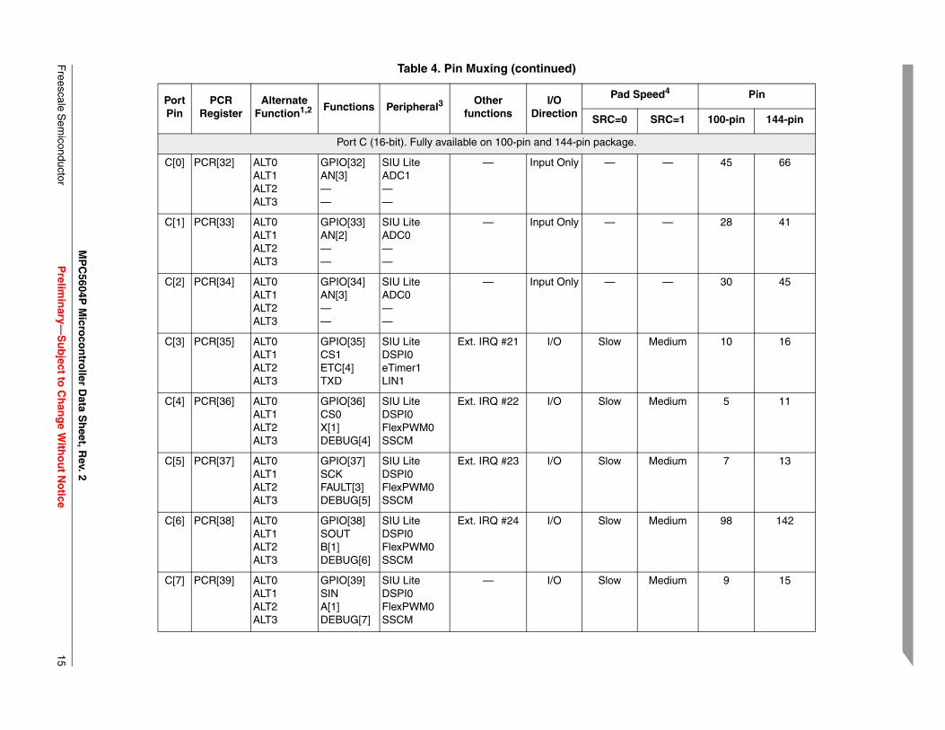
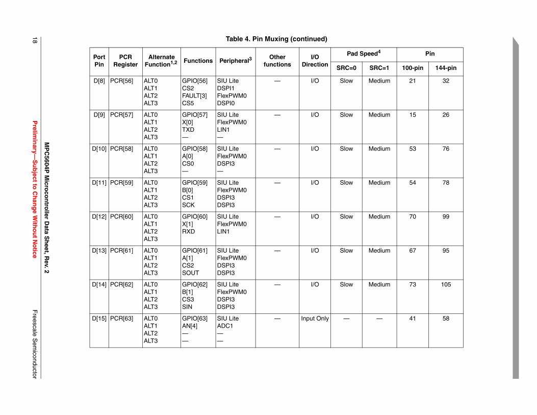
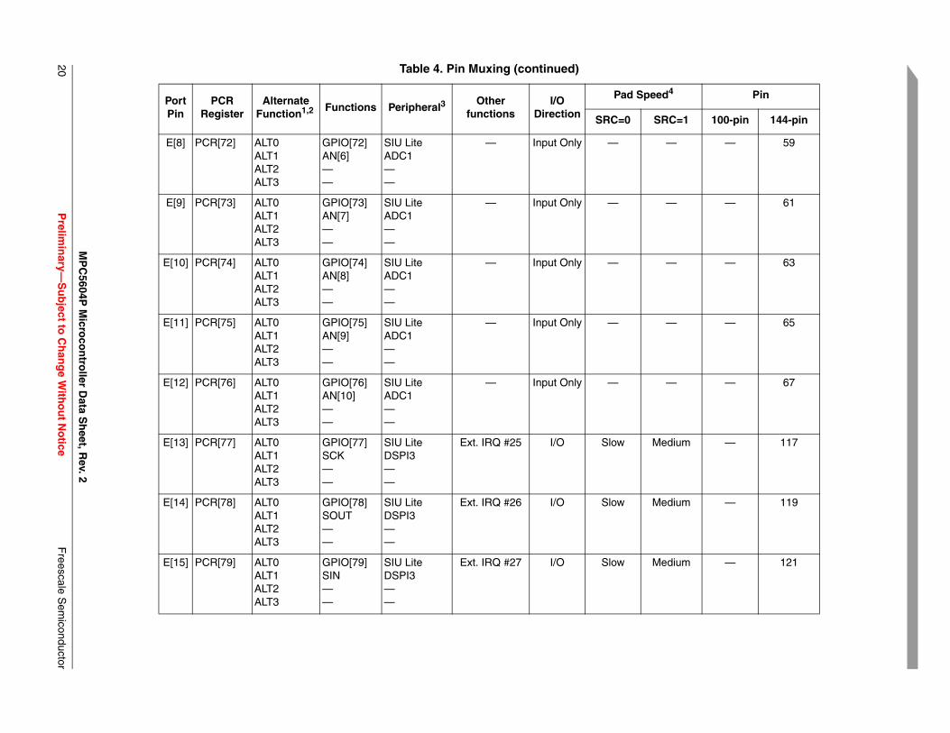
2.2.3 Pin MuxingTable 4 defines the pin list and muxing for the MPC5604P devices.
Each row of Table 4 shows all the possible ways of configuring each pin, via “alternate functions”. The default function assigned to each pin after reset is the ALT0 function.
Some pins have more than four alternate functions. These additional alternate functions are shown in the column “Other functions”. This column also contains information related to the External Interrupt capability and the boot configuration. Pins marked as external interrupt capable can also be used to resume from STOP and HALT mode.
MPC5604P devices provide four main I/O pad types depending of the associated functions:• Slow pads are the most common, providing a compromise between transition time and low electromagnetic emission.• Medium pads provide fast enough transition for serial communication channels with controlled current to reduce
electromagnetic emission.• Fast pads provide maximum speed. They are used for improved NEXUS debugging capability.• Symmetric pads are designed to meet FlexRay requirements.
Medium and Fast pads can use slow configuration to reduce electromagnetic emission, at the cost of reducing AC performance.
Table 3. System Pins
Symbol Description DirectionPad Speed1
1 SCR values refer to the value assigned to the Slew Rate Control bits of the pad configuration register
Pin
SRC=0 SRC=1 100-pin 144-pin
Dedicated pins. All pins available on 144-pin package. MDO 0 not available on 100-pin package.
MDO 0 Nexus Message Data Output - line 0 Output Only Slow Fast — 9
NMI Non Maskable Interrupt Input Only Slow — 1 1
XTAL Input for oscillator amplifier circuit and internal clock generator.
— — — 18 29
EXTAL Oscillator amplifier output — — — 19 30
TMS JTAG state machine control Bidirectional Slow Fast 59 87
TCK JTAG clock Input Only Slow — 60 88
Reset pin, available on 100-pin and 144-pin package.
RESET_B Bidirectional reset with Schmitt-Trigger characteristics andnoise filter
Bidirectional Medium — 20 31
Test pin, available on 100-pin and 144-pin package.
VPP TEST Pin for testing purpose only. To be tied to ground in normal operating mode.
— — — 74 107
MPC5604P Microcontroller Data Sheet, Rev. 2
Preliminary—Subject to Change Without Notice Freescale Semiconductor10

F
Pin
1 100-pin 144-pin
m 51 73
m 52 74
m 57 84
m 64 92
m 75 108
m 8 14
m 2 2
m 4 10
MP
C5604P
Micro
con
troller D
ata Sh
eet, Rev. 2
Prelim
inary—
Su
bject to
Ch
ang
e With
ou
t No
ticereescale S
emiconductor
11
Table 4. Pin Muxing
PortPin
PCR Register
Alternate Function1,2 Functions Peripheral3
Otherfunctions
I/O Direction
Pad Speed4
SRC=0 SRC=
Port A (16-bit). Fully available on 100-pin and 144-pin package.
A[0] PCR[0] ALT0ALT1ALT2ALT3
GPIO[0]ETC[0]SCKF[0]
SIU LiteeTimer0DSPI2FCU0
Ext. IRQ #0 I/O Slow Mediu
A[1] PCR[1] ALT0ALT1ALT2ALT3
GPIO[1]ETC[1]SOUTF[1]
SIU LiteeTimer0DSPI2FCU0
Ext. IRQ #1 I/O Slow Mediu
A[2] PCR[2] ALT0ALT1ALT2ALT3
GPIO[2]ETC[2]SINA[3]
SIU LiteeTimer0DSPI2FlexPWM0
Ext. IRQ #2Boot pin ABS[0]
I/O Slow Mediu
A[3] PCR[3] ALT0ALT1ALT2ALT3
GPIO[3]ETC[3]CS0B[3]
SIU LiteeTimer0DSPI2FlexPWM0
Ext. IRQ #3Boot pin ABS[2]
I/O Slow Mediu
A[4] PCR[4] ALT0ALT1ALT2ALT3
GPIO[4]ETC[0]CS1ETC[4]
SIU LiteeTimer1DSPI2eTimer0
Ext. IRQ #4Boot pin FAB
Weak pull down during
reset
I/O Slow Mediu
A[5] PCR[5] ALT0ALT1ALT2ALT3
GPIO[5]CS0ETC[5]CS7
SIU LiteDSPI1eTimer1DSPI0
Ext. IRQ #5 I/O Slow Mediu
A[6] PCR[6] ALT0ALT1ALT2ALT3
GPIO[6]SCK——
SIU LiteDSPI1——
Ext. IRQ #6 I/O Slow Mediu
A[7] PCR[7] ALT0ALT1ALT2ALT3
GPIO[7]SOUT——
SIU LiteDSPI1——
Ext. IRQ #7 I/O Slow Mediu

1
m 6 12
m 94 134
m 81 118
m 82 120
m 83 122
m 95 136
m 99 143
m 100 144
Pin
1 100-pin 144-pin
MP
C5604P
Micro
con
troller D
ata Sh
eet, Rev. 2
Prelim
inary—
Su
bject to
Ch
ang
e With
ou
t No
ticeF
reescale Sem
iconductor2
A[8] PCR[8] ALT0ALT1ALT2ALT3
GPIO[8]SIN——
SIU LiteDSPI1——
Ext. IRQ #8 I/O Slow Mediu
A[9] PCR[9] ALT0ALT1ALT2ALT3
GPIO[9]CS1FAULT[0]B[3]
SIU LiteDSPI2FlexPWM0FlexPWM0
— I/O Slow Mediu
A[10] PCR[10] ALT0ALT1ALT2ALT3
GPIO[10]CS0B[0]X[2]
SIU LiteDSPI2FlexPWM0FlexPWM0
Ext. IRQ #9 I/O Slow Mediu
A[11] PCR[11] ALT0ALT1ALT2ALT3
GPIO[11]SCKA[0]A[2]
SIU LiteDSPI2FlexPWM0FlexPWM0
Ext. IRQ #10 I/O Slow Mediu
A[12] PCR[12] ALT0ALT1ALT2ALT3
GPIO[12]SOUTA[2]B[2]
SIU LiteDSPI2FlexPWM0FlexPWM0
Ext. IRQ #11 I/O Slow Mediu
A[13] PCR[13] ALT0ALT1ALT2ALT3
GPIO[13]SINB[2]FAULT[0]
SIU LiteDSPI2FlexPWM0FlexPWM0
Ext. IRQ #12 I/O Slow Mediu
A[14] PCR[14] ALT0ALT1ALT2ALT3
GPIO[14]TXDETC[4]—
SIU LiteSafety Port0eTimer1—
Ext. IRQ #13 I/O Slow Mediu
A[15] PCR[15] ALT0ALT1ALT2ALT3
GPIO[15]RXDETC[5]—
SIU LiteSafety Port0eTimer1—
Ext. IRQ #14 I/O Slow Mediu
Table 4. Pin Muxing (continued)
PortPin
PCR Register
Alternate Function1,2 Functions Peripheral3
Otherfunctions
I/O Direction
Pad Speed4
SRC=0 SRC=

F
m 76 109
m 77 110
m 79 114
m 80 116
61 89
m 58 86
m 96 138
29 43
Pin
1 100-pin 144-pin
MP
C5604P
Micro
con
troller D
ata Sh
eet, Rev. 2
Prelim
inary—
Su
bject to
Ch
ang
e With
ou
t No
ticereescale S
emiconductor
13
Port B (16-bit). Fully available on 100-pin and 144-pin package.
B[0] PCR[16] ALT0ALT1ALT2ALT3
GPIO[16]TXDETC[2]DEBUG[0]
SIU LiteCAN0eTimer1SSCM
Ext. IRQ #15 I/O Slow Mediu
B[1] PCR[17] ALT0ALT1ALT2ALT3
GPIO[17]RXDETC[3]DEBUG[1]
SIU LiteCAN0eTimer1SSCM
Ext. IRQ #16 I/O Slow Mediu
B[2] PCR[18] ALT0ALT1ALT2ALT3
GPIO[18]TXD—DEBUG[2]
SIU LiteLIN0—SSCM
Ext. IRQ #17 I/O Slow Mediu
B[3] PCR[19] ALT0ALT1ALT2ALT3
GPIO[19]RXD—DEBUG[3]
SIU LiteLIN0—SSCM
— I/O Slow Mediu
B[4] PCR[20] ALT0ALT1ALT2ALT3
—TDO——
—JTAG0——
— I/O Slow Fast
B[5] PCR[21] ALT0ALT1ALT2ALT3
—TDI——
—JTAG0——
— I/O Slow Mediu
B[6] PCR[22] ALT0ALT1ALT2ALT3
GPIO[22]CLKOUTCS2—
SIU LiteControlDSPI2—
Ext. IRQ #18 I/O Slow Mediu
B[7] PCR[23] ALT0ALT1ALT2ALT3
GPIO[23]AN[0]RXD—
SIU LiteADC0LIN0—
— Input Only — —
Table 4. Pin Muxing (continued)
PortPin
PCR Register
Alternate Function1,2 Functions Peripheral3
Otherfunctions
I/O Direction
Pad Speed4
SRC=0 SRC=

1
31 47
35 52
36 53
37 54
38 55
42 60
44 64
43 62
Pin
1 100-pin 144-pin
MP
C5604P
Micro
con
troller D
ata Sh
eet, Rev. 2
Prelim
inary—
Su
bject to
Ch
ang
e With
ou
t No
ticeF
reescale Sem
iconductor4
B[8] PCR[24] ALT0ALT1ALT2ALT3
GPIO[24]AN[1]ETC[5]—
SIU LiteADC0eTimer0—
— Input Only — —
B[9] PCR[25] ALT0ALT1ALT2ALT3
GPIO[25]AN[11]——
SIU LiteADC0 - ADC1——
— Input Only — —
B[10] PCR[26] ALT0ALT1ALT2ALT3
GPIO[26]AN[12]——
SIU LiteADC0 - ADC1——
— Input Only — —
B[11] PCR[27] ALT0ALT1ALT2ALT3
GPIO[27]AN[13]——
SIU LiteADC0 - ADC1——
— Input Only — —
B[12] PCR[28] ALT0ALT1ALT2ALT3
GPIO[28]AN[14]——
SIU LiteADC0 - ADC1——
— Input Only — —
B[13] PCR[29] ALT0ALT1ALT2ALT3
GPIO[29]AN[0]RXD—
SIU LiteADC1LIN1—
— Input Only — —
B[14] PCR[30] ALT0ALT1ALT2ALT3
GPIO[30]AN[1]ETC[4]—
SIU LiteADC1eTimer0—
Ext. IRQ #19 Input Only — —
B[15] PCR[31] ALT0ALT1ALT2ALT3
GPIO[31]AN[2]——
SIU LiteADC1——
Ext. IRQ #20 Input Only — —
Table 4. Pin Muxing (continued)
PortPin
PCR Register
Alternate Function1,2 Functions Peripheral3
Otherfunctions
I/O Direction
Pad Speed4
SRC=0 SRC=
F
45 66
28 41
30 45
m 10 16
m 5 11
m 7 13
m 98 142
m 9 15
Pin
1 100-pin 144-pin
MP
C5604P
Micro
con
troller D
ata Sh
eet, Rev. 2
Prelim
inary—
Su
bject to
Ch
ang
e With
ou
t No
ticereescale S
emiconductor
15
Port C (16-bit). Fully available on 100-pin and 144-pin package.
C[0] PCR[32] ALT0ALT1ALT2ALT3
GPIO[32]AN[3]——
SIU LiteADC1——
— Input Only — —
C[1] PCR[33] ALT0ALT1ALT2ALT3
GPIO[33]AN[2]——
SIU LiteADC0——
— Input Only — —
C[2] PCR[34] ALT0ALT1ALT2ALT3
GPIO[34]AN[3]——
SIU LiteADC0——
— Input Only — —
C[3] PCR[35] ALT0ALT1ALT2ALT3
GPIO[35]CS1ETC[4]TXD
SIU LiteDSPI0eTimer1LIN1
Ext. IRQ #21 I/O Slow Mediu
C[4] PCR[36] ALT0ALT1ALT2ALT3
GPIO[36]CS0X[1]DEBUG[4]
SIU LiteDSPI0FlexPWM0SSCM
Ext. IRQ #22 I/O Slow Mediu
C[5] PCR[37] ALT0ALT1ALT2ALT3
GPIO[37]SCKFAULT[3]DEBUG[5]
SIU LiteDSPI0FlexPWM0SSCM
Ext. IRQ #23 I/O Slow Mediu
C[6] PCR[38] ALT0ALT1ALT2ALT3
GPIO[38]SOUTB[1]DEBUG[6]
SIU LiteDSPI0FlexPWM0SSCM
Ext. IRQ #24 I/O Slow Mediu
C[7] PCR[39] ALT0ALT1ALT2ALT3
GPIO[39]SINA[1]DEBUG[7]
SIU LiteDSPI0FlexPWM0SSCM
— I/O Slow Mediu
Table 4. Pin Muxing (continued)
PortPin
PCR Register
Alternate Function1,2 Functions Peripheral3
Otherfunctions
I/O Direction
Pad Speed4
SRC=0 SRC=

1
m 91 130
m 84 123
m 78 111
m 55 80
m 56 82
m 71 101
m 72 103
tric 85 124
Pin
1 100-pin 144-pin
MP
C5604P
Micro
con
troller D
ata Sh
eet, Rev. 2
Prelim
inary—
Su
bject to
Ch
ang
e With
ou
t No
ticeF
reescale Sem
iconductor6
C[8] PCR[40] ALT0ALT1ALT2ALT3
GPIO[40]CS1FAULT[2]CS6
SIU LiteDSPI1FlexPWM0DSPI0
— I/O Slow Mediu
C[9] PCR[41] ALT0ALT1ALT2ALT3
GPIO[41]CS3FAULT[2]X[3]
SIU LiteDSPI2FlexPWM0FlexPWM0
— I/O Slow Mediu
C[10] PCR[42] ALT0ALT1ALT2ALT3
GPIO[42]CS2FAULT[1]A[3]
SIU LiteDSPI2FlexPWM0FlexPWM0
— I/O Slow Mediu
C[11] PCR[43] ALT0ALT1ALT2ALT3
GPIO[43]ETC[4]CS2CS0
SIU LiteeTimer0DSPI2DSPI3
— I/O Slow Mediu
C[12] PCR[44] ALT0ALT1ALT2ALT3
GPIO[44]ETC[5]CS3CS1
SIU LiteeTimer0DSPI2DSPI3
— I/O Slow Mediu
C[13] PCR[45] ALT0ALT1ALT2ALT3
GPIO[45]ETC[1]EXT INEXT. SYNC
SIU LiteeTimer1ctu0FlexPWM0
— I/O Slow Mediu
C[14] PCR[46] ALT0ALT1ALT2ALT3
GPIO[46]ETC[2]EXT TGR—
SIU LiteeTimer1ctu0—
— I/O Slow Mediu
C[15] PCR[47] ALT0ALT1ALT2ALT3
GPIO[47]CA TR ENETC[0]A[1]
SIU LiteFlexRay0eTimer1FlexPWM0
ALT 4 Modectu0 EXT INALT 5 ModeFlexPWM0 EXT. SYNC
I/O Slow Symme
Table 4. Pin Muxing (continued)
PortPin
PCR Register
Alternate Function1,2 Functions Peripheral3
Otherfunctions
I/O Direction
Pad Speed4
SRC=0 SRC=

F
tric 86 125
m 3 3
m 97 140
tric 89 128
tric 90 129
m 22 33
m 23 34
m 26 37
Pin
1 100-pin 144-pin
MP
C5604P
Micro
con
troller D
ata Sh
eet, Rev. 2
Prelim
inary—
Su
bject to
Ch
ang
e With
ou
t No
ticereescale S
emiconductor
17
Port D (16-bit). Fully available on 100-pin and 144-pin package.
D[0] PCR[48] ALT0ALT1ALT2ALT3
GPIO[48]CA TXETC[1]B[1]
SIU LiteFlexRay0eTimer1FlexPWM0
— I/O Slow Symme
D[1] PCR[49] ALT0ALT1ALT2ALT3
GPIO[49]CA RXETC[2]EXT TRG
SIU LiteFlexRay0eTimer1ctu0
— I/O Slow Mediu
D[2] PCR[50] ALT0ALT1ALT2ALT3
GPIO[50]CB RXETC[3]X[3]
SIU LiteFlexRay0eTimer1FlexPWM0
— I/O Slow Mediu
D[3] PCR[51] ALT0ALT1ALT2ALT3
GPIO[51]CB TXETC[4]A[3]
SIU LiteFlexRay0eTimer1FlexPWM0
— I/O Slow Symme
D[4] PCR[52] ALT0ALT1ALT2ALT3
GPIO[52]CB TR ENETC[5]B[3]
SIU LiteFlexRay0eTimer1FlexPWM0
— I/O Slow Symme
D[5] PCR[53] ALT0ALT1ALT2ALT3
GPIO[53]CS3F[0]SOUT
SIU LiteDSPI0FCU0DSPI3
— I/O Slow Mediu
D[6] PCR[54] ALT0ALT1ALT2ALT3
GPIO[54]CS2SCKFAULT[1]
SIU LiteDSPI0DSPI3FlexPWM0
— I/O Slow Mediu
D[7] PCR[55] ALT0ALT1ALT2ALT3
GPIO[55]CS3F[1]SIN
SIU LiteDSPI1FCU0DSPI3
ALT 4 ModeDSPI0 CS4
I/O Slow Mediu
Table 4. Pin Muxing (continued)
PortPin
PCR Register
Alternate Function1,2 Functions Peripheral3
Otherfunctions
I/O Direction
Pad Speed4
SRC=0 SRC=
1
m 21 32
m 15 26
m 53 76
m 54 78
m 70 99
m 67 95
m 73 105
41 58
Pin
1 100-pin 144-pin
MP
C5604P
Micro
con
troller D
ata Sh
eet, Rev. 2
Prelim
inary—
Su
bject to
Ch
ang
e With
ou
t No
ticeF
reescale Sem
iconductor8
D[8] PCR[56] ALT0ALT1ALT2ALT3
GPIO[56]CS2FAULT[3]CS5
SIU LiteDSPI1FlexPWM0DSPI0
— I/O Slow Mediu
D[9] PCR[57] ALT0ALT1ALT2ALT3
GPIO[57]X[0]TXD—
SIU LiteFlexPWM0LIN1—
— I/O Slow Mediu
D[10] PCR[58] ALT0ALT1ALT2ALT3
GPIO[58]A[0]CS0—
SIU LiteFlexPWM0DSPI3—
— I/O Slow Mediu
D[11] PCR[59] ALT0ALT1ALT2ALT3
GPIO[59]B[0]CS1SCK
SIU LiteFlexPWM0DSPI3DSPI3
— I/O Slow Mediu
D[12] PCR[60] ALT0ALT1ALT2ALT3
GPIO[60]X[1]RXD
SIU LiteFlexPWM0LIN1
— I/O Slow Mediu
D[13] PCR[61] ALT0ALT1ALT2ALT3
GPIO[61]A[1]CS2SOUT
SIU LiteFlexPWM0DSPI3DSPI3
— I/O Slow Mediu
D[14] PCR[62] ALT0ALT1ALT2ALT3
GPIO[62]B[1]CS3SIN
SIU LiteFlexPWM0DSPI3DSPI3
— I/O Slow Mediu
D[15] PCR[63] ALT0ALT1ALT2ALT3
GPIO[63]AN[4]——
SIU LiteADC1——
— Input Only — —
Table 4. Pin Muxing (continued)
PortPin
PCR Register
Alternate Function1,2 Functions Peripheral3
Otherfunctions
I/O Direction
Pad Speed4
SRC=0 SRC=

F
package.
46 68
27 39
32 49
— 40
— 42
— 44
— 46
— 48
Pin
1 100-pin 144-pin
MP
C5604P
Micro
con
troller D
ata Sh
eet, Rev. 2
Prelim
inary—
Su
bject to
Ch
ang
e With
ou
t No
ticereescale S
emiconductor
19
Port E(16-bit). Fully available on 144-pin package. E[0], E[1] and E[2] available on 100-pin
E[0] PCR[64] ALT0ALT1ALT2ALT3
GPIO[64]AN[5]——
SIU LiteADC1——
— Input Only — —
E[1] PCR[65] ALT0ALT1ALT2ALT3
GPIO[65]AN[4]——
SIU LiteADC0——
— Input Only — —
E[2] PCR[66] ALT0ALT1ALT2ALT3
GPIO[66]AN[5]——
SIU LiteADC0——
— Input Only — —
E[3] PCR[67] ALT0ALT1ALT2ALT3
GPIO[67]AN[6]——
SIU LiteADC0——
— Input Only — —
E[4] PCR[68] ALT0ALT1ALT2ALT3
GPIO[68]AN[7]——
SIU LiteADC0——
— Input Only — —
E[5] PCR[69] ALT0ALT1ALT2ALT3
GPIO[69]AN[8]——
SIU LiteADC0——
— Input Only — —
E[6] PCR[70] ALT0ALT1ALT2ALT3
GPIO[70]AN[9]——
SIU LiteADC0——
— Input Only — —
E[7] PCR[71] ALT0ALT1ALT2ALT3
GPIO[71]AN[10]——
SIU LiteADC0——
— Input Only — —
Table 4. Pin Muxing (continued)
PortPin
PCR Register
Alternate Function1,2 Functions Peripheral3
Otherfunctions
I/O Direction
Pad Speed4
SRC=0 SRC=
2
— 59
— 61
— 63
— 65
— 67
m — 117
m — 119
m — 121
Pin
1 100-pin 144-pin
MP
C5604P
Micro
con
troller D
ata Sh
eet, Rev. 2
Prelim
inary—
Su
bject to
Ch
ang
e With
ou
t No
ticeF
reescale Sem
iconductor0
E[8] PCR[72] ALT0ALT1ALT2ALT3
GPIO[72]AN[6]——
SIU LiteADC1——
— Input Only — —
E[9] PCR[73] ALT0ALT1ALT2ALT3
GPIO[73]AN[7]——
SIU LiteADC1——
— Input Only — —
E[10] PCR[74] ALT0ALT1ALT2ALT3
GPIO[74]AN[8]——
SIU LiteADC1——
— Input Only — —
E[11] PCR[75] ALT0ALT1ALT2ALT3
GPIO[75]AN[9]——
SIU LiteADC1——
— Input Only — —
E[12] PCR[76] ALT0ALT1ALT2ALT3
GPIO[76]AN[10]——
SIU LiteADC1——
— Input Only — —
E[13] PCR[77] ALT0ALT1ALT2ALT3
GPIO[77]SCK——
SIU LiteDSPI3——
Ext. IRQ #25 I/O Slow Mediu
E[14] PCR[78] ALT0ALT1ALT2ALT3
GPIO[78]SOUT——
SIU LiteDSPI3——
Ext. IRQ #26 I/O Slow Mediu
E[15] PCR[79] ALT0ALT1ALT2ALT3
GPIO[79]SIN——
SIU LiteDSPI3——
Ext. IRQ #27 I/O Slow Mediu
Table 4. Pin Muxing (continued)
PortPin
PCR Register
Alternate Function1,2 Functions Peripheral3
Otherfunctions
I/O Direction
Pad Speed4
SRC=0 SRC=

F
m — 133
m — 135
m — 137
m — 139
— 4
— 5
— 8
— 19
Pin
1 100-pin 144-pin
MP
C5604P
Micro
con
troller D
ata Sh
eet, Rev. 2
Prelim
inary—
Su
bject to
Ch
ang
e With
ou
t No
ticereescale S
emiconductor
21
Port F (16-bit). Fully available on 144-pin package
F[0] PCR[80] ALT0ALT1ALT2ALT3
GPIO[80]DBG0CS3—
SIU LiteFlexRay0DSPI3—
Ext. IRQ #28 I/O Slow Mediu
F[1] PCR[81] ALT0ALT1ALT2ALT3
GPIO[81]DBG1CS2—
SIU LiteFlexRay0DSPI3—
Ext. IRQ #29 I/O Slow Mediu
F[2] PCR[82] ALT0ALT1ALT2ALT3
GPIO[82]DBG2CS1—
SIU LiteFlexRay0DSPI3—
— I/O Slow Mediu
F[3] PCR[83] ALT0ALT1ALT2ALT3
GPIO[83]DBG3CS0—
SIU LiteFlexRay0DSPI3—
— I/O Slow Mediu
F[4] PCR[84] ALT0ALT1ALT2ALT3
GPIO[84]MDO[3]——
SIU Litenexus0——
— I/O Slow Fast
F[5] PCR[85] ALT0ALT1ALT2ALT3
GPIO[85]MDO[2]——
SIU Litenexus0——
— I/O Slow Fast
F[6] PCR[86] ALT0ALT1ALT2ALT3
GPIO[86]MDO[1]——
SIU Litenexus0——
— I/O Slow Fast
F[7] PCR[87] ALT0ALT1ALT2ALT3
GPIO[87]MCKO——
SIU Litenexus0——
— I/O Slow Fast
Table 4. Pin Muxing (continued)
PortPin
PCR Register
Alternate Function1,2 Functions Peripheral3
Otherfunctions
I/O Direction
Pad Speed4
SRC=0 SRC=

2
— 20
— 23
— 24
m — 25
m — 106
m — 112
m — 115
m — 113
Pin
1 100-pin 144-pin
MP
C5604P
Micro
con
troller D
ata Sh
eet, Rev. 2
Prelim
inary—
Su
bject to
Ch
ang
e With
ou
t No
ticeF
reescale Sem
iconductor2
F[8] PCR[88] ALT0ALT1ALT2ALT3
GPIO[88]MSEO1——
SIU Litenexus0——
— I/O Slow Fast
F[9] PCR[89] ALT0ALT1ALT2ALT3
GPIO[89]MSEO0——
SIU Litenexus0——
— I/O Slow Fast
F[10] PCR[90] ALT0ALT1ALT2ALT3
GPIO[90]EVTO——
SIU Litenexus0——
— I/O Slow Fast
F[11] PCR[91] ALT0ALT1ALT2ALT3
GPIO[91]EVTI——
SIU Litenexus0——
— I/O Slow Mediu
F[12] PCR[92] ALT0ALT1ALT2ALT3
GPIO[92]ETC[3]——
SIU LiteeTimer1——
— I/O Slow Mediu
F[13] PCR[93] ALT0ALT1ALT2ALT3
GPIO[93]ETC[4]——
SIU LiteeTimer1——
— I/O Slow Mediu
F[14] PCR[94] ALT0ALT1ALT2ALT3
GPIO[94]TXD——
SIU LiteLIN1——
— I/O Slow Mediu
F[15] PCR[95] ALT0ALT1ALT2ALT3
GPIO[95]RXD——
SIU LiteLIN1——
— I/O Slow Mediu
Table 4. Pin Muxing (continued)
PortPin
PCR Register
Alternate Function1,2 Functions Peripheral3
Otherfunctions
I/O Direction
Pad Speed4
SRC=0 SRC=

F
m — 38
m — 141
m — 102
m — 104
m — 100
m — 85
m — 98
m — 83
Pin
1 100-pin 144-pin
MP
C5604P
Micro
con
troller D
ata Sh
eet, Rev. 2
Prelim
inary—
Su
bject to
Ch
ang
e With
ou
t No
ticereescale S
emiconductor
23
Port G (12-bit). Fully available on 144-pin package.
G[0] PCR[96] ALT0ALT1ALT2ALT3
GPIO[96]F[0]——
SIU LiteFCU0——
Ext. IRQ #30 I/O Slow Mediu
G[1] PCR[97] ALT0ALT1ALT2ALT3
GPIO[97]F[1]——
SIU LiteFCU0——
Ext. IRQ #31 I/O Slow Mediu
G[2] PCR[98] ALT0ALT1ALT2ALT3
GPIO[98]X[2]——
SIU LiteFlexPWM0——
— I/O Slow Mediu
G[3] PCR[99] ALT0ALT1ALT2ALT3
GPIO[99]A[2]——
SIU LiteFlexPWM0——
— I/O Slow Mediu
G[4] PCR[100] ALT0ALT1ALT2ALT3
GPIO[100]B[2]——
SIU LiteFlexPWM0——
— I/O Slow Mediu
G[5] PCR[101] ALT0ALT1ALT2ALT3
GPIO[101]X[3]——
SIU LiteFlexPWM0——
— I/O Slow Mediu
G[6] PCR[102] ALT0ALT1ALT2ALT3
GPIO[102]A[3]——
SIU LiteFlexPWM0——
— I/O Slow Mediu
G[7] PCR[103] ALT0ALT1ALT2ALT3
GPIO[103]B[3]——
SIU LiteFlexPWM0——
— I/O Slow Mediu
Table 4. Pin Muxing (continued)
PortPin
PCR Register
Alternate Function1,2 Functions Peripheral3
Otherfunctions
I/O Direction
Pad Speed4
SRC=0 SRC=

2
m — 81
m — 79
m — 77
m — 75
= 00 -> Option 0; PCR.PA = tions; to use one of the input or this reason, the value
Pin
1 100-pin 144-pin
MP
C5604P
Micro
con
troller D
ata Sh
eet, Rev. 2
Prelim
inary—
Su
bject to
Ch
ang
e With
ou
t No
ticeF
reescale Sem
iconductor4
G[8] PCR[104] ALT0ALT1ALT2ALT3
GPIO[104]FAULT[0]——
SIU LiteFlexPWM0——
— I/O Slow Mediu
G[9] PCR[105] ALT0ALT1ALT2ALT3
GPIO[105]FAULT[1]——
SIU LiteFlexPWM0——
— I/O Slow Mediu
G[10] PCR[106] ALT0ALT1ALT2ALT3
GPIO[106]FAULT[2]——
SIU LiteFlexPWM0——
— I/O Slow Mediu
G[11] PCR[107] ALT0ALT1ALT2ALT3
GPIO[107]FAULT[3]——
SIU LiteFlexPWM0——
— I/O Slow Mediu
1 ALT0 is the primary (default) function for each port after reset.2 Alternate functions are chosen by setting the values of the PCR.PA bitfields inside the SIU module. PCR.PA
01 -> Option 1; PCR.PA = 10 -> Option 2; PCR.PA = 11-> Option 3. This is intended to select the output funcfunctions, the PCR.IBE bit must be written to ‘1’, regardless of the values selected in the PCR.PA bitfields. Fcorresponding to an input only function is reported as “—”.
3 Module included on the MCU.4 Programmable via the SRC (Slew Rate Control) bits in the respective Pad Configuration Register.
Table 4. Pin Muxing (continued)
PortPin
PCR Register
Alternate Function1,2 Functions Peripheral3
Otherfunctions
I/O Direction
Pad Speed4
SRC=0 SRC=

3 Electrical characteristicsThis section contains detailed information on power considerations, DC/AC electrical characteristics, and AC timing specifications for the MPC5604P MCU.
The electrical specifications are preliminary and are from previous designs, design simulations, or initial evaluation. These specifications may not be fully tested or guaranteed at this early stage of the product life cycle, however for production silicon these specifications will be met. Finalized specifications will be published after complete characterization and device qualifications have been completed.
In the tables where the device logic provides signals with their respective timing characteristics, the symbol “CC” for Controller Characteristics is included in the Symbol column.
In the tables where the external system must provide signals with their respective timing characteristics to the device, the symbol “SR” for System Requirement is included in the Symbol column.
3.1 Absolute Maximum RatingsTable 5. Absolute Maximum Ratings1
Symbol Parameter Conditions Min Max2 Unit
VDD_HV_REG SR 3.3 V / 5.0 V voltage regulator supply voltage
— -0.3 5.5 V
VDD_HV_IOx SR 3.3 V / 5.0 V input/output supply voltage
— -0.3 5.5 V
VSS_HV_IOx SR Input/output ground voltage — -0.1 0.1 V
VDD_HV_FL SR 3.3 V / 5.0 V code and data flash supply voltage
— -0.3 3.6 / 5.5 V
VSS_HV_FL SR Code and data flash ground — -0.1 0.1 V
VDD_HV_OSC SR 3.3 V / 5.0 V crystal oscillator amplifier supply voltage
— -0.3 5.5 V
VSS_HV_OSC SR 3.3 V / 5.0 V crystal oscillator amplifier reference voltage
— -0.1 0.1 V
VDD_HV_AD03 SR 3.3 V / 5.0 V ADC0 supply and high
reference voltage— - 0.3 5.5 V
VSS_HV_AD0 SR ADC0 ground and low reference voltage
— -0.1 0.1 V
VDD_HV_AD13 SR 3.3 V / 5.0 V ADC1 supply and high
reference voltage— - 0.3 5.5 V
VSS_HV_AD1 SR ADC1 ground and low reference voltage
— -0.1 0.1 V
TVDD SR Slope characteristics on all VDD during power up4
— — 0.25 V/µs
MPC5604P Microcontroller Data Sheet, Rev. 2
Preliminary—Subject to Change Without NoticeFreescale Semiconductor 25

3.2 Recommended Operating Conditions
VIN SR Voltage on any pin with respect to ground (VSS_HV_IOx)
— -0.3 5.5 V
Relative to VDD_HV_IOx
-0.3 VDD_HV_IOx + 0.35
IINJPAD SR Injected input current on any pin during overload condition
— -10 10 mA
IINJSUM SR Absolute sum of all injected input currents during overload condition
— -50 50 mA
TSTG SR Storage temperature — -55 150 °C
1 Functional operating conditions are given in the DC electrical characteristics. Absolute maximum ratings are stress ratings only, and functional operation at the maxima is not guaranteed. Stress beyond the listed maxima may affect device reliability or cause permanent damage to the device.
2 Absolute maximum voltages are currently maximum burn-in voltages. Absolute maximum specifications for device stress have not yet been determined.
3 The power supply voltage must be identical for ADC0 and ADC1 (both at 3.3 V or both at 5 V).4 Guaranteed by device validation5 Only when VDD_HV_IOx <5.2 V
Table 6. Recommended Operating Conditions (5.0 V)
Symbol Parameter Conditions Min Max1 Unit
VDD_HV_REG SR 5.0 V voltage regulator supply voltage — 4.5 5.5 V
VDD_HV_IOx SR 5.0 V input/output supply voltage — 4.5 5.5 V
VSS_HV_IOx SR Input/output ground voltage — 0 0 V
VDD_HV_FL SR 5.0 V code and data flash supply voltage — 4.5 5.5 V
VSS_HV_FL SR Code and data flash ground — 0 0 V
VDD_HV_OSC SR 5.0 V crystal oscillator amplifier supply voltage
— 4.5 5.5 V
VSS_HV_OSC SR 5.0 V crystal oscillator amplifier reference voltage
— 0 0 V
VDD_HV_AD02 SR 5.0 V ADC0 supply and high reference
voltage— 4.5 5.5 V
VSS_HV_AD0 SR ADC0 ground and low reference voltage — 0 0 V
VDD_HV_AD12 SR 5.0 V ADC1 supply and high reference
voltage— 4.5 5.5 V
VSS_HV_AD1 SR ADC1 ground and low reference voltage — 0 0 V
VDD_LV_REGCOR3,4 SR Internal supply voltage — — — V
VSS_LV_REGCOR3 SR Internal reference voltage — 0 0 V
VDD_LV_CORx3,4 SR Internal supply voltage — — — V
VSS_LV_CORx3 SR Internal reference voltage — 0 0 V
Table 5. Absolute Maximum Ratings1 (continued)
Symbol Parameter Conditions Min Max2 Unit
MPC5604P Microcontroller Data Sheet, Rev. 2
Preliminary—Subject to Change Without Notice Freescale Semiconductor26

VDD_LV_PLL3,4,5 SR Internal supply voltage — — — V
VSS_LV_PLL3,5 SR Internal reference voltage — 0 0 V
TA SR Ambient temperature under bias fCPU = 64 MHz -40 105 °C
TJ SR Junction temperature under bias — -40 150 °C
1 Full functionality cannot be guaranteed when voltage drops below 4.5 V. In particular, ADC electrical characteristics and I/Os DC electrical specification may not be guaranteed.
2 The power supply voltage must be identical for ADC0 and ADC13 To be connected to emitter of external NPN. Low voltage supplies are not under user control—they are produced
by an on-chip voltage regulator—but for the device to function properly the low voltage grounds (VSS_LV_xxx) must be shorted to high voltage grounds (VSS_HV_xxx) and the low voltage supply pins (VDD_LV_xxx) must be connected to the external ballast emitter.
4 The low voltage supplies (VDD_LV_xxx) are not all independent.
• VDD_LV_COR1 and VDD_LV_COR2 are shorted internally via double bonding connections with lines that provide the low voltage supply to the data flash module. The integrity of the connections are monitored by an on-chip supply and ground comparator. Similarly, VSS_LV_COR1 and VSS_LV_COR2 are internally shorted and monitored.
• VDD_LV_REGCOR and VDD_LV_RECORx are physically shorted internally, as are VSS_LV_REGCOR and VSS_LV_CORx.
• VDD_LV_PLL and VSS_LV_PLL are independent of other supplies.5 Low voltage supply/ground lines of the FMPLLs internally are physically separate but are shorted with a
double-bonding connection on the VDD_LV_PLL and VSS_LV_PLL pins.
Table 7. Recommended Operating Conditions (3.3 V)
Symbol Parameter Conditions Min Max1 Unit
VDD_HV_REG SR 3.3 V voltage regulator supply voltage — 3.0 3.6 V
VDD_HV_IOx SR 3.3 V input/output supply voltage — 3.0 3.6 V
VSS_HV_IOx SR Input/output ground voltage — 0 0 V
VDD_HV_FL SR 3.3 V code and data flash supply voltage — 3.0 3.6 V
VSS_HV_FL SR Code and data flash ground — 0 0 V
VDD_HV_OSC SR 3.3 V crystal oscillator amplifier supply voltage
— 3.0 3.6 V
VSS_HV_OSC SR 3.3 V crystal oscillator amplifier reference voltage
— 0 0 V
VDD_HV_AD02 SR 3.3 V ADC0 supply and high reference
voltage— 3.0 3.6 V
VSS_HV_AD0 SR ADC0 ground and low reference voltage — 0 0 V
VDD_HV_AD12 SR 3.3 V ADC1 supply and high reference
voltage— 3.0 3.6 V
VSS_HV_AD1 SR ADC1 ground and low reference voltage — 0 0 V
VDD_LV_REGCOR3,4 SR Internal supply voltage — — — V
Table 6. Recommended Operating Conditions (5.0 V) (continued)
Symbol Parameter Conditions Min Max1 Unit
MPC5604P Microcontroller Data Sheet, Rev. 2
Preliminary—Subject to Change Without NoticeFreescale Semiconductor 27

3.3 Thermal Characteristics
VSS_LV_REGCOR3 SR Internal reference voltage — 0 0 V
VDD_LV_CORx3,4 SR Internal supply voltage — — — V
VSS_LV_CORx3 SR Internal reference voltage — 0 0 V
VDD_LV_PLL3,4,5 SR Internal supply voltage — — — V
VSS_LV_PLL3,5 SR Internal reference voltage — 0 0 V
TA SR Ambient temperature under bias fCPU = 64 MHz -40 105 °C
TJ SR Junction temperature under bias — -40 150 °C
1 Full functionality cannot be guaranteed when voltage drops below 3.0 V. In particular, ADC electrical characteristics and I/Os DC electrical specification may not be guaranteed.
2 The power supply voltage must be identical for ADC0 and ADC1. As long as that condition is met, ADC0 and ADC1 can be operated at 5 V with the rest of the device operating at 3.3 V.
3 To be connected to emitter of external NPN. Low voltage supplies are not under user control—they are produced by an on-chip voltage regulator—but for the device to function properly the low voltage grounds (VSS_LV_xxx) must be shorted to high voltage grounds (VSS_HV_xxx) and the low voltage supply pins (VDD_LV_xxx) must be connected to the external ballast emitter.
4 The low voltage supplies (VDD_LV_xxx) are not all independent.
VDD_LV_COR1 and VDD_LV_COR2 are shorted internally via double bonding connections with lines that provide the low voltage supply to the data flash module. The integrity of the connections are monitored by an on-chip supply and ground comparator. Similarly, VSS_LV_COR1 and VSS_LV_COR2 are internally shorted and monitored.
VDD_LV_REGCOR and VDD_LV_RECORx are physically shorted internally, as are VSS_LV_REGCOR and VSS_LV_CORx.
VDD_LV_PLL and VSS_LV_PLL are independent of other supplies.5 Low voltage supply/ground lines of the FMPLLs internally are physically separate but are shorted with a
double-bonding connection on the VDD_LV_PLL and VSS_LV_PLL pins.
Table 8. Thermal Characteristics for 144-pin LQFP1
1 Thermal characteristics are targets based on simulation that are subject to change per device characterization.
No. Symbol Parameter Conditions Value Unit
1 RθJA CC Thermal resistance junction-to-ambient, natural convection2
Single layer board - 1s 52 °C/W
2 RθJA CC Thermal resistance junction-to-ambient, natural convection2
Four layer board - 2s2p 43 °C/W
3 RθJMA CC Thermal resistance junction-to-ambient2 @ 200 ft./min.3, single layer board - 1s 43 °C/W
4 RθJMA CC Thermal resistance junction-to-ambient2 @ 200 ft./min.3, four layer board - 2s2p 37 °C/W
5 RθJB CC Thermal resistance junction to board4 31 °C/W
6 RθJCtop CC Thermal resistance junction to case (top)5 12 °C/W
7 ΨJT CC Junction to package top natural convection6 2 °C/W
Table 7. Recommended Operating Conditions (3.3 V) (continued)
Symbol Parameter Conditions Min Max1 Unit
MPC5604P Microcontroller Data Sheet, Rev. 2
Preliminary—Subject to Change Without Notice Freescale Semiconductor28
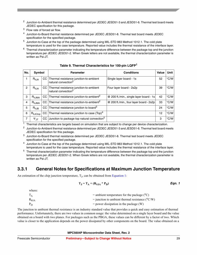
3.3.1 General Notes for Specifications at Maximum Junction TemperatureAn estimation of the chip junction temperature, TJ, can be obtained from Equation 1:
TJ = TA + (RθJA * PD) Eqn. 1
where:TA = ambient temperature for the package (oC)RθJA = junction to ambient thermal resistance (oC/W)PD = power dissipation in the package (W)
The junction to ambient thermal resistance is an industry standard value that provides a quick and easy estimation of thermal performance. Unfortunately, there are two values in common usage: the value determined on a single layer board and the value obtained on a board with two planes. For packages such as the PBGA, these values can be different by a factor of two. Which value is closer to the application depends on the power dissipated by other components on the board. The value obtained on a
2 Junction-to-Ambient thermal resistance determined per JEDEC JESD51-3 and JESD51-6. Thermal test board meets JEDEC specification for this package.
3 Flow rate of forced air flow.4 Junction-to-Board thermal resistance determined per JEDEC JESD51-8. Thermal test board meets JEDEC
specification for the specified package.5 Junction-to-Case at the top of the package determined using MIL-STD 883 Method 1012.1. The cold plate
temperature is used for the case temperature. Reported value includes the thermal resistance of the interface layer.6 Thermal characterization parameter indicating the temperature difference between the package top and the junction
temperature per JEDEC JESD51-2. When Greek letters are not available, the thermal characterization parameter is written as Psi-JT.
Table 9. Thermal Characteristics for 100-pin LQFP1
1 Thermal characteristics are targets based on simulation that are subject to change per device characterization.
No. Symbol Parameter Conditions Value Unit
1 RθJA CC Thermal resistance junction-to-ambient natural convection2
2 Junction-to-Ambient thermal resistance determined per JEDEC JESD51-3 and JESD51-6. Thermal test board meets JEDEC specification for this package.
Single layer board - 1s 52 °C/W
2 RθJA CC Thermal resistance junction-to-ambient natural convection2
Four layer board - 2s2p 39 °C/W
3 RθJMA CC Thermal resistance junction-to-ambient2 @ 200 ft./min., single layer board - 1s 42 °C/W
4 RθJMA CC Thermal resistance junction-to-ambient2 @ 200 ft./min., four layer board - 2s2p 33 °C/W
5 RθJB CC Thermal resistance junction to board3
3 Junction-to-Board thermal resistance determined per JEDEC JESD51-8. Thermal test board meets JEDEC specification for the specified package.
24 °C/W
6 RθJCtop CC Thermal resistance junction to case (Top)4
4 Junction-to-Case at the top of the package determined using MIL-STD 883 Method 1012.1. The cold plate temperature is used for the case temperature. Reported value includes the thermal resistance of the interface layer.
12 °C/W
7 ΨJT CC Junction to package top natural convection5
5 Thermal characterization parameter indicating the temperature difference between the package top and the junction temperature per JEDEC JESD51-2. When Greek letters are not available, the thermal characterization parameter is written as Psi-JT.
3 °C/W
MPC5604P Microcontroller Data Sheet, Rev. 2
Preliminary—Subject to Change Without NoticeFreescale Semiconductor 29

single layer board is appropriate for the tightly packed printed circuit board. The value obtained on the board with the internal planes is usually appropriate if the board has low power dissipation and the components are well separated.
When a heat sink is used, the thermal resistance is expressed in Equation 2 as the sum of a junction to case thermal resistance and a case to ambient thermal resistance:
RθJA = RθJC + RθCA Eqn. 2
where:RθJA = junction to ambient thermal resistance (°C/W)RθJC = junction to case thermal resistance (°C/W)RθCA = case to ambient thermal resistance (°C/W)
RθJC is device related and cannot be influenced by the user. The user controls the thermal environment to change the case to ambient thermal resistance, RθCA. For instance, the user can change the size of the heat sink, the air flow around the device, the interface material, the mounting arrangement on printed circuit board, or change the thermal dissipation on the printed circuit board surrounding the device.
To determine the junction temperature of the device in the application when heat sinks are not used, the Thermal Characterization Parameter (ΨJT) can be used to determine the junction temperature with a measurement of the temperature at the top center of the package case using Equation 3:
TJ = TT + (ΨJT x PD) Eqn. 3
where:TT = thermocouple temperature on top of the package (°C)ΨJT = thermal characterization parameter (°C/W)PD = power dissipation in the package (W)
The thermal characterization parameter is measured per JESD51-2 specification using a 40 gauge type T thermocouple epoxied to the top center of the package case. The thermocouple should be positioned so that the thermocouple junction rests on the package. A small amount of epoxy is placed over the thermocouple junction and over about 1 mm of wire extending from the junction. The thermocouple wire is placed flat against the package case to avoid measurement errors caused by cooling effects of the thermocouple wire.
References:
Semiconductor Equipment and Materials International3081 Zanker RoadSan Jose, CA 95134U.S.A.(408) 943-6900
MIL-SPEC and EIA/JESD (JEDEC) specifications are available from Global Engineering Documents at 800-854-7179 or 303-397-7956.
JEDEC specifications are available on the WEB at http://www.jedec.org.
1. C.E. Triplett and B. Joiner, An Experimental Characterization of a 272 PBGA Within an Automotive Engine Controller Module, Proceedings of SemiTherm, San Diego, 1998, pp. 47-54.
2. G. Kromann, S. Shidore, and S. Addison, Thermal Modeling of a PBGA for Air-Cooled Applications, Electronic Packaging and Production, pp. 53-58, March 1998.
3. B. Joiner and V. Adams, Measurement and Simulation of Junction to Board Thermal Resistance and Its Application in Thermal Modeling, Proceedings of SemiTherm, San Diego, 1999, pp. 212-220.
MPC5604P Microcontroller Data Sheet, Rev. 2
Preliminary—Subject to Change Without Notice Freescale Semiconductor30

3.4 Electromagnetic Interference (EMI) CharacteristicsTable 10. EMI Testing Specifications (Normal Mode)1,2,3
1 Normal mode: FlexPWM, 2nd PLL, FlexRay, 125 °C2 EMI testing and I/O port waveforms per SAE J1752/3 issued 1995-03 and IEC 61967-1, 23 TBD: To be defined
No. Symbol Parameter Conditions Min Typ Max Unit
1 — SR Scan range TBD TBD TBD MHz
2 — SR Operating frequency TBD TBD TBD MHz
3 VDD_LV_REGCORVDD_LV_CORxVDD_LV_PLL
SR LV operating voltages TBD TBD TBD V
4 VDD_HV_REGVDD_HV_AD1VDD_HV_AD0VDD_HV_FL
VDD_HV_OSCVDD_HV_IOx
SR HV operating voltages TBD TBD TBD V
5 VDD_HV_REGVDD_HV_AD1VDD_HV_AD0VDD_HV_FL
VDD_HV_OSCVDD_HV_IOx
CC Maximum amplitude Device settings chosen for worst-case emissions from typical use configuration.
TBD TBD TBD dBµV
6 VDD_HV_REGVDD_HV_AD1VDD_HV_AD0VDD_HV_FL
VDD_HV_OSCVDD_HV_IOx
CC Maximum amplitude No PLL frequency modulation
TBD TBD TBD dBµV
7 VDD_HV_REGVDD_HV_AD1VDD_HV_AD0VDD_HV_FL
VDD_HV_OSCVDD_HV_IOx
CC Maximum amplitude ±2% PLL frequency modulation
TBD TBD TBD dBµV
8 TA SR Operating temperature TBD TBD TBD °C
MPC5604P Microcontroller Data Sheet, Rev. 2
Preliminary—Subject to Change Without NoticeFreescale Semiconductor 31
3.5 Electrostatic Discharge (ESD) Characteristics
Table 11. EMI Testing Specifications (Airbag Mode)1,2,3
1 Airbag mode: No flexPWM, no 2nd PLL, no FlexRay, 105 °C2 EMI testing and I/O port waveforms per SAE J1752/3 issued 1995-03 and IEC 61967-1, 23 TBD: To be defined
Symbol Parameter Conditions Min Typ Max Unit
— SR Scan range TBD TBD TBD MHz
— SR Operating frequency TBD TBD TBD MHz
VDD_LV_REGCORVDD_LV_CORxVDD_LV_PLL
SR LV operating voltages TBD TBD TBD V
VDD_HV_REGVDD_HV_AD1VDD_HV_AD0VDD_HV_FL
VDD_HV_OSCVDD_HV_IOx
SR HV operating voltages TBD TBD TBD V
VDD_HV_REGVDD_HV_AD1VDD_HV_AD0VDD_HV_FL
VDD_HV_OSCVDD_HV_IOx
CC Maximum amplitude Device settings chosen for worst-case emissions from typical use configuration.
TBD TBD TBD dBµV
VDD_HV_REGVDD_HV_AD1VDD_HV_AD0VDD_HV_FL
VDD_HV_OSCVDD_HV_IOx
CC Maximum amplitude No PLL frequency modulation
TBD TBD TBD dBµV
VDD_HV_REGVDD_HV_AD1VDD_HV_AD0VDD_HV_FL
VDD_HV_OSCVDD_HV_IOx
CC Maximum amplitude ±2% PLL frequency modulation
TBD TBD TBD dBµV
TA SR Operating temperature TBD TBD TBD °C
Table 12. ESD ratings1,2
1 All ESD testing is in conformity with CDF-AEC-Q100 Stress Test Qualification for Automotive Grade Integrated Circuits.
Symbol Parameter Conditions Value Unit
VESD(HBM) SR Electrostatic discharge (Human Body Model) 2000 V
VESD(CDM) SR Electrostatic discharge (Charged Device Model) 750 (corners) V
500 (other)
MPC5604P Microcontroller Data Sheet, Rev. 2
Preliminary—Subject to Change Without Notice Freescale Semiconductor32

3.6 Voltage Regulator Electrical CharacteristicsThe internal voltage regulator requires an external NPN (BCP56 or BCP68) ballast to be connected as shown in Figure 4 as well as an external capacitance (CREG) to be connected to the device in order to provide a stable low voltage digital supply to the device. Capacitances should be placed on the board as near as possible to the associated pins. Care should also be taken to limit the serial inductance of the board to less than 15 nH.
For the MPC5604P microcontroller , 10 µF should be placed between each of the three VDD_LV_CORx/VSS_LV_CORx supply pairs and also between the VDD_LV_REGCOR/VSS_LV_REGCOR pair. Additionally, 40 μF should be placed between the VDD_HV_REG/VSS_HV_REG pins.
VDD = 3.0 V to 3.6 V / 4.5 V to 5.5 V, TA = -40 to 125 °C, unless otherwise specified.
Figure 4. External NPN Ballast Connections
2 A device will be defined as a failure if after exposure to ESD pulses the device no longer meets the device specification requirements. Complete DC parametric and functional testing shall be performed per applicable device specification at room temperature followed by hot temperature, unless specified otherwise in the device specification
Table 13. Voltage Regulator Electrical Characteristics1
No. Symbol Parameter Conditions Min Max Unit
1 VDD_HV_REG SR Power supply — 3.0 5.5 V
2 TJ SR Junction temperature — -40 150 °C
3 IREG CC Current consumption Reference included,
@ 55 °C No load — 2 mA
@ Full load — 11
4 IL CC Output current capacity DC load current — 400 mA
5 VDD_LV_REGCOR CC Output voltage (value @ IL = 0 @ 27°C) Pre-trimming sigma < 7 mV
— 1.330 V
Post-trimming 1.270 1.280
Output voltage (value @ IL = Imax) Post-trimming 1.145 —
6 SR External decoupling/stability capacitor 4 capacitances of 10 µF each
4 × 10 µF
ESR of external cap 0.05 0.2 Ω
1 bond wire R + 1 pad R 0.2 1 Ω
BCTRL
VDD_HV_REG
VDD_LV_REGCOR
MPC5604P Microcontroller Data Sheet, Rev. 2
Preliminary—Subject to Change Without NoticeFreescale Semiconductor 33

3.7 Power Up/Down SequencingThe maximum slope (TVDD) must be granted on all power supplies (see Table 5).
3.8 DC electrical Characteristics
3.8.1 NVUSRO RegisterPortions of the MPC5604P device configuration, i.e., high voltage supply, oscillator margin, and watchdog enable/disable after reset) are controlled via bit values in the NVUSRO register. NVUSRO[PAD3V5V] controls the device configuration as follows:
The DC electrical characteristics in the following sections are dependent on the PAD3V5V value as described above.
3.8.2 DC Electrical Characteristics (5 V)Table 15 gives the DC electrical characteristics at 5 V (4.5 V < VDD_HV_IOx < 5.5 V, NVUSRO[PAD3V5V]=0).
7 CC Number of pins for external decoupling/stability capacitor2
—4 — —
8 CC Internal parasitic filter capacitance — 10 50 nF
9 LBOND CC Bonding Inductance for Bipolar Base Control pad
—0 15 nH
10 CC Power supply rejection
@ DC @ no load Cload = 10 µF * 4 — -30 dB
@ 200 kHz @ no load — -100
@ DC @ 400 mA — -30
@ 200 kHz @ 400 mA — -30
11 CC Load current transient Cload = 10 µF * 4 — 10% to 90% of IL (max) in
100 ns
12 tSU CC Start-up time after input supply stabilizes
Cload = 10 µF * 4 — 500 µs
1 All values in this table are PRELIMINARY.2 See Table 2 for location of decoupling capacitors.
Table 14. NVUSRO[PAD3V5V] Field Description1
1 See the MPC5604P Reference Manual for more information on the NVUSRO register.
Value2
2 Default manufacturing value before flash initialization is '1' (3.3 V).
Description
0 High Voltage supply is 5.0 V
1 High Voltage supply is 3.3 V
Table 13. Voltage Regulator Electrical Characteristics1 (continued)
No. Symbol Parameter Conditions Min Max Unit
MPC5604P Microcontroller Data Sheet, Rev. 2
Preliminary—Subject to Change Without Notice Freescale Semiconductor34

Table 15. DC Electrical Characteristics (5.0 V, NVUSRO[PAD3V5V]=0)1
1 These specifications are design targets and subject to change per device characterization.
Symbol Parameter Conditions Min Max Unit
VIL SR Low level input voltage -0.12
2 “SR” parameter values must not exceed the absolute maximum ratings shown in Table 5.
0.35 VDD_HV_IOx V
VIH SR High level input voltage 0.65 VDD_HV_IOx VDD_HV_IOx + 0.12 V
VHYS CC Schmitt trigger hysteresis 0.1 VDD_HV_IOx — V
VOL_S CC Slow, low level output voltage IOL = 3 mA — 0.1 VDD_HV_IOx V
VOH_S CC Slow, high level output voltage IOH = -3 mA 0.8VDD_HV_IOx — V
VOL_M CC Medium, low level output voltage IOL = 3 mA — 0.1 VDD_HV_IOx V
VOH_M CC Medium, high level output voltage IOH = -3 mA 0.8 VDD_HV_IOx — V
VOL_F CC Fast, low level output voltage IOL = 3 mA — 0.1 VDD_HV_IOx V
VOH_F CC Fast, high level output voltage IOH = -3 mA 0.8 VDD_HV_IOx — V
VOL_SYM CC Symmetric, low level output voltage IOL = 3 mA — 0.1 VDD_HV_IOx V
VOH_SYM CC Symmetric, high level output voltage IOH = -3 mA 0.8 VDD_HV_IOx — V
IPU CC Equivalent pull-up current VIN = VIL -130 — µA
VIN = VIH — -10
IPD CC Equivalent pull-down current VIN = VIL 10 — µA
VIN = VIH — 130
IIL CC Input leakage current (all bidirectional ports)
TA = -40 to 125 °C
— 1 μA µA
IIL CC Input leakage current (all ADC input-only ports)
TA = -40 to 125 °C
— 0.5 μA µA
VILR SR RESET_B, low level input voltage -0.12 0.35 VDD_HV_IOx V
VIHR SR RESET_B, high level input voltage 0.65 VDD_HV_IOx VDD_HV_IOx + 0.12 V
VHYSR CC RESET_B, Schmitt trigger hysteresis 0.1 VDD_HV_IOx — V
VOLR CC RESET_B, low level output voltage IOL = 3 mA — 0.1 VDD_HV_IOx V
IPUR CC RESET_B, equivalent pull-up current VIN = VIL -130 — µA
VIN = VIH — -10
MPC5604P Microcontroller Data Sheet, Rev. 2
Preliminary—Subject to Change Without NoticeFreescale Semiconductor 35

3.8.3 DC Electrical characteristics (3.3 V)Table 18 gives the DC electrical characteristics at 3.3 V (3.0 V < VDD_HV_IOx < 3.6 V, NVUSRO[PAD3V5V]=1).
Table 16. Supply Current (5.0 V, NVUSRO[PAD3V5V]=0, Normal Mode)1,2,3
1 Normal mode: FlexPWM, ADCs, CTU, DSPI, LINFlex, FlexCAN, 15 output pins, 1st and 2nd PLL enabled, 125 °C ambient. I/O supply current excluded.
2 Values to be confirmed by characterization.3 TBD: To be defined.
Symbol Parameter Conditions Value Unit
IDD CC Supply Current
RUN (fetch from flash) VDD_LV_COREexternally forced at 1.3 V
40 MHz 92 mA
64 MHz 100
HALT VDD_LV_COREexternally forced at 1.3 V
TBD TBD
TBD
STOP VDD_LV_COREexternally forced at 1.3 V
TBD TBD
TBD
Table 17. Supply Current (5.0 V, NVUSRO[PAD3V5V]=0, Airbag Mode)1,2,3
1 Airbag mode: DSPI, LINFlex, FlexCAN, 15 output pins, 1st PLL only, 105 °C ambient. I/O supply current excluded.2 Values to be confirmed by characterization.3 TBD: To be defined.
Symbol Parameter Conditions Value Unit
IDD CC Supply Current
RUN (fetch from flash) VDD_LV_COREexternally forced at 1.3 V
40 MHz 64 mA
64 MHz 74
HALT VDD_LV_COREexternally forced at 1.3 V
TBD TBD
TBD
STOP VDD_LV_COREexternally forced at 1.3 V
TBD TBD
TBD
Table 18. DC Electrical Characteristics (3.3 V, NVUSRO[PAD3V5V]=1)1
Symbol Parameter Conditions Min Max Unit
VIL SR Low level input voltage -0.12 0.35 VDD_HV_IOx V
VIH SR High level input voltage 0.65 VDD_HV_IOx VDD_HV_IOx + 0.12
V
VHYS CC Schmitt trigger hysteresis 0.1 VDD_HV_IOx — V
VOL_S CC Slow, low level output voltage IOL = 1.5 mA — 0.5 V
VOH_S CC Slow, high level output voltage IOH = -1.5 mA VDD_HV_IOx - 0.8 — V
VOL_M CC Medium, low level output voltage IOL = 2 mA — 0.5 V
VOH_M CC Medium, high level output voltage IOH = -2 mA VDD_HV_IOx - 0.8 — V
VOL_F CC Fast, high level output voltage IOL = 1.5 mA — 0.5 V
MPC5604P Microcontroller Data Sheet, Rev. 2
Preliminary—Subject to Change Without Notice Freescale Semiconductor36

VOH_F CC Fast, high level output voltage IOH = -1.5 mA VDD_HV_IOx - 0.8 — V
VOL_SYM CC Symmetric, high level output voltage IOL = 1.5 mA — 0.5 V
VOH_SYM CC Symmetric, high level output voltage IOH = -1.5 mA VDD_HV_IOx - 0.8 — V
IPU CC Equivalent pull-up current VIN = VIL -130 — µA
VIN = VIH — -10
IPD CC Equivalent pull-down current VIN = VIL 10 — µA
VIN = VIH — 130
IIL CC Input leakage current (all bidirectional ports)
TA = -40 to 125 °C
— 1 μA µA
IIL CC Input leakage current (all ADC input-only ports)
TA = -40 to 125 °C
— 0.5 μA µA
VILR SR RESET_B, low level input voltage -0.12 0.35 VDD_HV_IOx V
VIHR SR RESET_B, high level input voltage 0.65 VDD_HV_IOx VDD_HV_IOx + 0.12
V
VHYSR CC RESET_B, Schmitt trigger hysteresis 0.1 VDD_HV_IOx — V
VOLR CC RESET_B, low level output voltage IOL = 1.5 mA — 0.5 V
IPUR CC RESET_B, equivalent pull-up current VIN = VIL -130 — µA
VIN = VIH — -10
1 These specifications are design targets and subject to change per device characterization.2 “SR” parameter values must not exceed the absolute maximum ratings shown in Table 5.
Table 19. Supply Current (3.3 V, NVUSRO[PAD3V5V]=1, Normal Mode)1,2,3
1 Normal mode: FlexPWM, ADCs, CTU, DSPI, LINFlex, FlexCAN, 15 output pins, 1st and 2nd PLL enabled, 125 °C ambient. I/O supply current excluded.
2 Values to be confirmed by characterization.3 TBD: To be defined.
Symbol Parameter Conditions Value Unit
IDD CC Supply Current
RUN (fetch from flash) VDD_LV_COREexternally forced at 1.3 V
40 MHz 89 mA
64 MHz 98
HALT VDD_LV_COREexternally forced at 1.3 V
TBD TBD
TBD
STOP VDD_LV_COREexternally forced at 1.3 V
TBD TBD
TBD
Table 18. DC Electrical Characteristics (3.3 V, NVUSRO[PAD3V5V]=1)1 (continued)
Symbol Parameter Conditions Min Max Unit
MPC5604P Microcontroller Data Sheet, Rev. 2
Preliminary—Subject to Change Without NoticeFreescale Semiconductor 37

3.9 Temperature Sensor Electrical Characteristics
3.10 Main Oscillator Electrical CharacteristicsThe MPC5604P provides an oscillator/resonator driver.
Table 20. Supply Current (3.3 V, NVUSRO[PAD3V5V]=1, Airbag Mode)1,2,3
1 Airbag mode: DSPI, LINFlex, FlexCAN, 15 output pins, 1st PLL only, 105 °C ambient. I/O supply current excluded.2 Values to be confirmed by characterization.3 TBD: To be defined.
Symbol Parameter Conditions Value Unit
IDD CC Supply Current
RUN (fetch from flash) VDD_LV_COREexternally forced at 1.3 V
40 MHz 62 mA
64 MHz 72
HALT VDD_LV_COREexternally forced at 1.3 V
TBD TBD
TBD
STOP VDD_LV_COREexternally forced at 1.3 V
TBD TBD
TBD
Table 21. Temperature Sensor Electrical Characteristics
Symbol Parameter Conditions Value Unit
— CC Sensitivity 5.1 mV/°C
— CC Accuracy TJ = -40 to 100 °C ±3.0 °C
TJ = 100 to 150 °C ±5.0 °C
Table 22. Main Oscillator Electrical Characteristics (5.0 V, NVUSRO[PAD3V5V]=0)
Symbol Parameter Min Typ Max Unit
fOSC SR Oscillator frequency 4 — 40 MHz
gm CC Transconductance 9.0 13.2 17.0 mA/V
VOSC CC Oscillation amplitude on EXTAL pin 1.3 — 2.25 V
IOSC CC Power consumption (analog supply RMS current in oscillator mode) — — 2.5 mA
tOSCSU CC Start-up time1
1 The start-up time is dependent upon crystal characteristics, board leakage, etc., high ESR and excessive capacitive loads can cause long start-up time.
8 — — ms
MPC5604P Microcontroller Data Sheet, Rev. 2
Preliminary—Subject to Change Without Notice Freescale Semiconductor38

3.11 FMPLL Electrical Characteristics
3.12 16 MHz RC Oscillator Electrical Characteristics
Table 23. Main Oscillator Electrical Characteristics (3.3 V, NVUSRO[PAD3V5V]=1)
Symbol Parameter Min Typ Max Unit
fOSC SR Oscillator frequency 4 — 40 MHz
gm CC Transconductance 8.0 13.2 16.0 mA/V
VOSC CC Oscillation amplitude on EXTAL pin 1.3 — 2.25 V
IOSC CC Power consumption (analog supply RMS current in oscillator mode) — — 2.2 mA
tOSCSU CC Start-up time1
1 The start-up time is dependent upon crystal characteristics, board leakage, etc., high ESR and excessive capacitive loads can cause long start-up time.
8 — — ms
Table 24. Input Clock Characteristics
Symbol Parameter Min Typ Max Unit
fOSC SR Oscillator frequency 4 — 40 MHz
fCLK CC Frequency in bypass and 1:1 mode — — 100 MHz
trCLK CC Rise/fall time in bypass and 1:1 mode — — 1 ns
tDC CC Duty cycle 47.5 50 52.5 %
Table 25. FMPLL Electrical Characteristics
Symbol Parameter Conditions Min Typ Max Unit
fFMPLLOUT CC Clock frequency range in normal mode
— 4 — 120 MHz
fFREE CC Free running frequency 20 150 MHz
tLOCK CC Lock time Stable oscillator (fFMPLLIN = 4 MHz),stable VDD_LV_PLL
— — 200 µs
ΔtPKJIT CC Single period jitter (peak to peak) fFMPLLOUT @ 16 MHz,fFMPLLIN @ 4 MHz
— — ±500 ps
ΔtLTJIT CC Long term jitter fFMPLLOUT @ 16 MHz,fFMPLLIN @ 4 MHz
— — ±6 ns
Table 26. 16 MHz RC Oscillator Electrical Characteristics
Symbol Parameter Conditions Min Typ Max Unit
fRC CC RC oscillator frequency before trimming 27 °- 150 °C 10 — 22 MHz
RC oscillator frequency after trimming 27 °C — 16 —
MPC5604P Microcontroller Data Sheet, Rev. 2
Preliminary—Subject to Change Without NoticeFreescale Semiconductor 39

IRCRUN CC Current consumption in running mode — — 2001 µA
CC RC oscillator precision before trimming — — — ±15 %
ΔRCMVAR CC Frequency Spread: The variation in output frequency from PTF2 across temperature and the supply voltage range
— — — ±5 %
ΔRCMTRIM CC Post Trim Accuracy: The variation of the PTF2 from the 16 MHz
27 °C — — ±2 %
1 Current consumption is the sum of current from the VDD_LV_CORx pin (150 μA) and the VDD_HV_REG pin (50 μA).2 PTF = Post Trimming Frequency: The frequency of the output clock after trimming at typical supply voltage and
temperature
Table 26. 16 MHz RC Oscillator Electrical Characteristics (continued)
Symbol Parameter Conditions Min Typ Max Unit
MPC5604P Microcontroller Data Sheet, Rev. 2
Preliminary—Subject to Change Without Notice Freescale Semiconductor40

3.13 Analog-to-Digital Converter (ADC) Electrical CharacteristicsThe device provides a 10-bit Successive Approximation Register (SAR) Analog-to-Digital Converter.
Figure 5. ADC Characteristics and Error Definitions
3.13.1 Input Impedance and ADC AccuracyIn the following analysis, the input circuit corresponding to the precise channels is considered.
To preserve the accuracy of the A/D converter, it is necessary that analog input pins have low AC impedance. Placing a capacitor with good high frequency characteristics at the input pin of the device can be effective: the capacitor should be as large as possible, ideally infinite. This capacitor contributes to attenuating the noise present on the input pin; further, it sources charge during the sampling phase, when the analog signal source is a high-impedance source.
A real filter can typically be obtained by using a series resistance with a capacitor on the input pin (simple RC filter). The RC filtering may be limited according to the value of source impedance of the transducer or circuit supplying the analog signal to
(2)
(1)
(3)
(4)
(5)
Offset Error OSE
Offset Error OSE
Gain Error GE
1 LSB (ideal)
Vin(A) (LSBideal)
(1) Example of an actual transfer curve
(2) The ideal transfer curve
(3) Differential non-linearity error (DNL)
(4) Integral non-linearity error (INL)
(5) Center of a step of the actual transfer curve
code out
1023
1022
1021
1020
1019
1018
5
4
3
2
1
0
7
6
1 2 3 4 5 6 7 1017 1018 1019 1020 1021 1022 1023
1 LSB ideal = VDD_ADC / 1024
MPC5604P Microcontroller Data Sheet, Rev. 2
Preliminary—Subject to Change Without NoticeFreescale Semiconductor 41

be measured. The filter at the input pins must be designed taking into account the dynamic characteristics of the input signal (bandwidth) and the equivalent input impedance of the ADC itself.
In fact a current sink contributor is represented by the charge sharing effects with the sampling capacitance: CS being substantially a switched capacitance, with a frequency equal to the conversion rate of the ADC, it can be seen as a resistive path to ground. For instance, assuming a conversion rate of 1 MHz, with CS equal to 3 pF, a resistance of 330 kΩ is obtained (REQ = 1 / (fc×CS), where fc represents the conversion rate at the considered channel). To minimize the error induced by the voltage partitioning between this resistance (sampled voltage on CS) and the sum of RS + RF + RL + RSW + RAD, the external circuit must be designed to respect the Equation 4:
Eqn. 4
Equation 4 generates a constraint for external network design, in particular on resistive path. Internal switch resistances (RSW and RAD) can be neglected with respect to external resistances.
Figure 6. Input Equivalent Circuit (Precise Channels)
VARS RF RL RSW RAD+ + + +
REQ---------------------------------------------------------------------------• 1
2--- LSB<
RF
CF
RS RL RSW1
CP2 CS
VDD
SamplingSource Filter Current Limiter
EXTERNAL CIRCUIT INTERNAL CIRCUIT SCHEME
RS Source ImpedanceRF Filter ResistanceCF Filter CapacitanceRL Current Limiter ResistanceRSW1 Channel Selection Switch ImpedanceRAD Sampling Switch ImpedanceCP Pin Capacitance (two contributions, CP1 and CP2)CS Sampling Capacitance
CP1
RAD
ChannelSelection
VA
MPC5604P Microcontroller Data Sheet, Rev. 2
Preliminary—Subject to Change Without Notice Freescale Semiconductor42

Figure 7. Input Equivalent Circuit (Extended Channels)
A second aspect involving the capacitance network shall be considered. Assuming the three capacitances CF, CP1 and CP2 are initially charged at the source voltage VA (refer to the equivalent circuit reported in Figure 6): A charge sharing phenomenon is installed when the sampling phase is started (A/D switch close).
Figure 8. Transient Behavior during Sampling Phase
In particular two different transient periods can be distinguished:• A first and quick charge transfer from the internal capacitance CP1 and CP2 to the sampling capacitance CS occurs (CS
is supposed initially completely discharged): considering a worst case (since the time constant in reality would be faster) in which CP2 is reported in parallel to CP1 (call CP = CP1 + CP2), the two capacitances CP and CS are in series, and the time constant is
RF
CF
RS RL RSW1
CP3 CS
VDD
SamplingSource Filter Current Limiter
EXTERNAL CIRCUIT INTERNAL CIRCUIT SCHEME
RS Source ImpedanceRF Filter ResistanceCF Filter CapacitanceRL Current Limiter ResistanceRSW Channel Selection Switch Impedance (two contributions RSW1 and RSW2)RAD Sampling Switch ImpedanceCP Pin Capacitance (three contributions, CP1, CP2 and CP3)CS Sampling Capacitance
CP1
RAD
ChannelSelection
VA CP2
Extended
RSW2
Switch
VA
VA1
VA2
tTS
VCS Voltage Transient on CS
ΔV < 0.5 LSB
1 2
τ1 < (RSW + RAD) CS << TS
τ2 = RL (CS + CP1 + CP2)
MPC5604P Microcontroller Data Sheet, Rev. 2
Preliminary—Subject to Change Without NoticeFreescale Semiconductor 43

Eqn. 5
Equation 5 can again be simplified considering only CS as an additional worst condition. In reality, the transient is faster, but the A/D converter circuitry has been designed to be robust also in the very worst case: the sampling time TS is always much longer than the internal time constant:
Eqn. 6
The charge of CP1 and CP2 is redistributed also on CS, determining a new value of the voltage VA1 on the capacitance according to Equation 7:
Eqn. 7
• A second charge transfer involves also CF (that is typically bigger than the on-chip capacitance) through the resistance RL: again considering the worst case in which CP2 and CS were in parallel to CP1 (since the time constant in reality would be faster), the time constant is:
Eqn. 8
In this case, the time constant depends on the external circuit: in particular imposing that the transient is completed well before the end of sampling time TS, a constraints on RL sizing is obtained:
Eqn. 9
Of course, RL shall be sized also according to the current limitation constraints, in combination with RS (source impedance) and RF (filter resistance). Being CF definitively bigger than CP1, CP2 and CS, then the final voltage VA2 (at the end of the charge transfer transient) will be much higher than VA1. Equation 10 must be respected (charge balance assuming now CS already charged at VA1):
Eqn. 10
The two transients above are not influenced by the voltage source that, due to the presence of the RFCF filter, is not able to provide the extra charge to compensate the voltage drop on CS with respect to the ideal source VA; the time constant RFCF of the filter is very high with respect to the sampling time (TS). The filter is typically designed to act as anti-aliasing.
τ1 RSW RAD+( )=CP CS•
CP CS+---------------------•
τ1 RSW RAD+( )< CS TS«•
VA1 CS CP1 CP2+ +( )• VA CP1 CP2+( )•=
τ2 RL< CS CP1 CP2+ +( )•
10 τ2• 10 RL CS CP1 CP2+ +( )••= TS<
VA2 CS CP1 CP2 CF+ + +( )• VA CF• VA1+ CP1 CP2+ CS+( )•=
MPC5604P Microcontroller Data Sheet, Rev. 2
Preliminary—Subject to Change Without Notice Freescale Semiconductor44

Figure 9. Spectral Representation of Input Signal
Calling f0 the bandwidth of the source signal (and as a consequence the cut-off frequency of the anti-aliasing filter, fF), according to the Nyquist theorem the conversion rate fC must be at least 2f0; it means that the constant time of the filter is greater than or at least equal to twice the conversion period (TC). Again the conversion period TC is longer than the sampling time TS, which is just a portion of it, even when fixed channel continuous conversion mode is selected (fastest conversion rate at a specific channel): in conclusion it is evident that the time constant of the filter RFCF is definitively much higher than the sampling time TS, so the charge level on CS cannot be modified by the analog signal source during the time in which the sampling switch is closed.
The considerations above lead to impose new constraints on the external circuit, to reduce the accuracy error due to the voltage drop on CS; from the two charge balance equations above, it is simple to derive Equation 11 between the ideal and real sampled voltage on CS:
Eqn. 11
From this formula, in the worst case (when VA is maximum, that is for instance 5 V), assuming to accept a maximum error of half a count, a constraint is evident on CF value:
Eqn. 12
f0 f
Analog Source Bandwidth (VA)
f0 f
Sampled Signal Spectrum (fC = conversion Rate)
fCf
Anti-Aliasing Filter (fF = RC Filter pole)
fF
2 f0 ≤ fC (Nyquist)
fF = f0 (Anti-aliasing Filtering Condition)
TC ≤ 2 RFCF (Conversion Rate vs. Filter Pole)
Noise
VAVA2------------
CP1 CP2+ CF+
CP1 CP2+ CF CS+ +--------------------------------------------------------=
CF 2048 CS•>
MPC5604P Microcontroller Data Sheet, Rev. 2
Preliminary—Subject to Change Without NoticeFreescale Semiconductor 45

3.13.2 ADC Input Leakage Current
3.13.3 ADC Conversion Characteristics
Table 27. ADC Input Leakage Current
Symbol Parameter Conditions Typ Unit
IIL1
1 Current measured at analog input pad for the A/D, which is associated to a single A/D (12 channels out of 16 are dedicated to a single A/D, while 4 are shared—Port B[9:12]. This pad has two serial switches simultaneously controlled with worst leakage at 143 nA (TARGET).
CC Input leakage current -40 °C Pad = Low 2.3 pA
Pad = High 0.4 pA
85 °C Pad = Low 3.76 nA
Pad = High 8.12 nA
125 °C Pad = Low 15.2 nA
Pad = High 53.2 nA
150 °C Pad = Low 36.8 nA
Pad = High 143.5 nA
IIL2
2 Current measured at analog input shared between ADC_0 and ADC_1. In this case two parallel instantiations of the dual switch are present and thus the leakage doubles (286 nA).
CC Input leakage current -40 °C Pad = Low 6.89 pA
Pad = High 17 fA
85 °C Pad = Low 7.5 nA
Pad = High 16.2 nA
125 °C Pad = Low 29.2 nA
Pad = High 106.1 nA
150 °C Pad = Low 66.42 nA
Pad = High 286.1 nA
Table 28. ADC Conversion Characteristics
Symbol Parameter Conditions1Value2
UnitMin Max
fCK CC ADC Clock frequency (depends on ADC configuration)(The duty cycle depends on AD_ck3 frequency)
34 60 MHz
fs CC Sampling frequency — 1.53 MHz
tADC_C CC Conversion time5 fADC = 20 MHz6,ADC_conf_comp = 3
0.625 µs
CS7,8 CC ADC input sampling
capacitance— 2.5 pF
MPC5604P Microcontroller Data Sheet, Rev. 2
Preliminary—Subject to Change Without Notice Freescale Semiconductor46

CP17,8 CC ADC input pin capacitance
1— 0.89 pF
CP27,8 CC ADC input pin capacitance
2— 1 pF
CP37,8 CC ADC input pin capacitance
3— 1 pF
RSW17,8 CC Internal resistance of
analog source— 0.6 kΩ
RSW27,8 CC Internal resistance of
analog source— 0.7 kΩ
RAD7,8 CC Internal resistance of
analog source— 2 kΩ
IINJ Input current injection Current injection on one ADC input, different from the converted one
-10 10 mA
INL CC Integral Non Linearity No overload -1.5 1.5 LSB
DNL CC Differential Non Linearity No overload -1.0 1.0 LSB
OFS CC Offset error After offset cancellation -1.0 1.0 LSB
GNE CC Gain error -1.0 1.0 LSB
TUE CC Total unadjusted error After offset cancellation -2.0 2.0 LSB
SINAD CC Signal to noise and distortion
Max input dynamic, after offset cancellation
55.9 — dB
THD CC Total harmonic distortion Max input dynamic, after offset cancellation
59 — dB
ENOB CC Effective number of bits Max input dynamic, after offset cancellation
9.0 — bit
TUEP CC Total Unadjusted Error for precise channels, input only pins
No overload -2 2 LSB
TUEX CC Total Unadjusted Error for extended channel
No overload -3 3 LSB
1 VDD = 3.3 V to 3.6 V / 5.0 V to 5.5 V, TA = -40 to +125 °C, unless otherwise specified.2 All values need to be confirmed during device validation.3 AD_CK clock is always half of the ADC module input clock defined via the auxiliary clock divider for the ADC.4 When configured to allow 60 MHz ADC, the minimum ADC clock speed is 9 MHz, below which precision is lost.5 This parameter does not include the sample time tADC_S, but only the time for determining the digital result and the
time to load the result register with the conversion result. 6 20 MHz ADC clock. Specific prescaler is programmed on MC_PLL_CLK to provide 20 MHz clock to the ADC.7 See Figure 7.8 Guaranteed by design9 Does not include packaging and bonding capacitances
Table 28. ADC Conversion Characteristics (continued)
Symbol Parameter Conditions1Value2
UnitMin Max
MPC5604P Microcontroller Data Sheet, Rev. 2
Preliminary—Subject to Change Without NoticeFreescale Semiconductor 47

3.14 Flash Memory Electrical CharacteristicsTable 29. Program and Erase Specifications1
1 TBD: To be defined
Symbol Parameter Min ValueTypical Value2
2 Typical program and erase times assume nominal supply values and operation at 25 °C. All times are subject to change pending device characterization.
Initial Max3
3 Initial factory condition: < 100 program/erase cycles, 25 °C, typical supply voltage.
Max4
4 The maximum program & erase times occur after the specified number of program/erase cycles. These maximum values are characterized but not guaranteed.
Unit
Tdwprogram Double Word (64 bits) Program Time5
5 Actual hardware programming times. This does not include software overhead.
— TBD 22 500 μs
T16kpperase 16 KB Block Pre-program and Erase Time — TBD 500 5000 ms
T32kpperase 32 KB Block Pre-program and Erase Time — TBD 600 5000 ms
T128kpperase 128 KB Block Pre-program and Erase Time — TBD 1300 7500 ms
Table 30. Flash Module Life1
1 TBD: To be defined
Symbol Parameter ConditionsValue
UnitMin Typ
P/E Number of program/erase cycles per block for 16 Kbyte blocks over the operating temperature range (TJ)
— 100,000 — cycles
P/E Number of program/erase cycles per block for 32 Kbyte blocks over the operating temperature range (TJ)
— 10,000 100,000(TBD)
cycles
P/E Number of program/erase cycles per block for 128 Kbyte blocks over the operating temperature range (TJ)
— 1,000 100,000(TBD)
cycles
Retention Minimum data retention at 85 °C average ambient temperature2
2 Ambient temperature averaged over duration of application, not to exceed recommended product operating temperature range.
Blocks with 0 - 1,000 P/E cycles
20 — years
Blocks with 10,000 P/E cycles
10 — years
Blocks with 100,000 P/E cycles
1 - 5 (TBD)
— years
MPC5604P Microcontroller Data Sheet, Rev. 2
Preliminary—Subject to Change Without Notice Freescale Semiconductor48

3.15 AC Specifications
3.15.1 Pad AC SpecificationsTable 31 gives the AC electrical characteristics at 5 V (4.5 V < VDD_HV_IOx < 5.5 V, NVUSRO[PAD3V5V]=0) operation.
Table 32 gives the AC electrical characteristics at 3.3 V (3.0 V < VDD_HV_IOx < 3.6 V, NVUSRO[PAD3V5V]=1) operation.
Table 31. Pad AC Specifications (5.0 V, NVUSRO[PAD3V5V]=0)1
1 Propagation delay from VDD_HV_IOx/2 of internal signal to Pchannel/Nchannel switch-on condition
No. Pad
Tswitchon1
(ns)Rise/Fall2
(ns)
2 Slope at rising/falling edge
Frequency(MHz)
Current slew3
(mA/ns)
3 Data based on characterization results, not tested in production
Load drive(pF)
Min Typ Max Min Typ Max Min Typ Max Min Typ Max
1 Slow 1.5 — 30 6 — 50 — — 4 0.04 — 2 25
1.5 — 30 9 — 100 — — 2 0.04 — 2 50
1.5 — 30 12 — 125 — — 2 0.04 — 2 100
1.5 — 30 16 — 150 — — 2 0.04 — 2 200
2 Medium 1 — 15 3 — 10 — — 40 2.5 — 7 25
1 — 15 5 — 20 — — 20 2.5 — 7 50
1 — 15 9 — 40 — — 13 2.5 — 8 100
1 — 15 12 — 70 — — 7 2.5 — 8 200
3 Fast 1 — 6 1 — 4 — — 100 18 — 55 25
1 — 6 1.5 — 6 — — 80 18 — 55 50
1 — 6 3 — 12 — — 40 18 — 55 100
1 — 6 5 — 16 — — 25 18 — 55 200
4 Symmetric 1 — 5 1 — 4 — — 50 10 — 25 25
5 Pull Up/Down(5.5 V max)
— — — — — 5000 — — — — — — 50
Table 32. Pad AC Specifications (3.3 V, INVUSRO[PAD3V5V]=1)1
No. Pad
Tswitchon1
(ns)Rise/Fall2
(ns)Frequency
(MHz)Current slew3
(mA/ns) Load drive(pF)
Min Typ Max Min Typ Max Min Typ Max Min Typ Max
1 Slow 3 — 40 4 — 40 — — 4 0.01 — 2 25
3 — 40 6 — 50 — — 2 0.01 — 2 50
3 — 40 10 — 75 — — 2 0.01 — 2 100
3 — 40 14 — 100 — — 2 0.01 — 2 200
MPC5604P Microcontroller Data Sheet, Rev. 2
Preliminary—Subject to Change Without NoticeFreescale Semiconductor 49

Figure 10. Pad Output Delay
2 Medium 1 — 15 2 — 12 — — 40 2.5 — 7 25
1 — 15 4 — 25 — — 20 2.5 — 7 50
1 — 15 8 — 40 — — 13 2.5 — 7 100
1 — 15 14 — 70 — — 7 2.5 — 7 200
3 Fast 1 — 6 1 — 4 — — 72 3 — 40 25
1 — 6 1.5 — 7 — — 55 7 — 40 50
1 — 6 3 — 12 — — 40 7 — 40 100
1 — 6 5 — 18 — — 25 7 — 40 200
4 Symmetric 1 — 8 1 — 5 — — 50 3 — 25 25
5 Pull Up/Down(3.6 V max)
— — — — — 7500 — — — — — — 50
1 Propagation delay from VDD_HV_IOx/2 of internal signal to Pchannel/Nchannel switch-on condition2 Slope at rising/falling edge3 Data based on characterization results, not tested in production
Table 32. Pad AC Specifications (3.3 V, INVUSRO[PAD3V5V]=1)1 (continued)
No. Pad
Tswitchon1
(ns)Rise/Fall2
(ns)Frequency
(MHz)Current slew3
(mA/ns) Load drive(pF)
Min Typ Max Min Typ Max Min Typ Max Min Typ Max
VDD_HV_IOx/2
VOH
VOL
RisingEdgeOutputDelay
FallingEdgeOutputDelay
PadData Input
PadOutput
MPC5604P Microcontroller Data Sheet, Rev. 2
Preliminary—Subject to Change Without Notice Freescale Semiconductor50
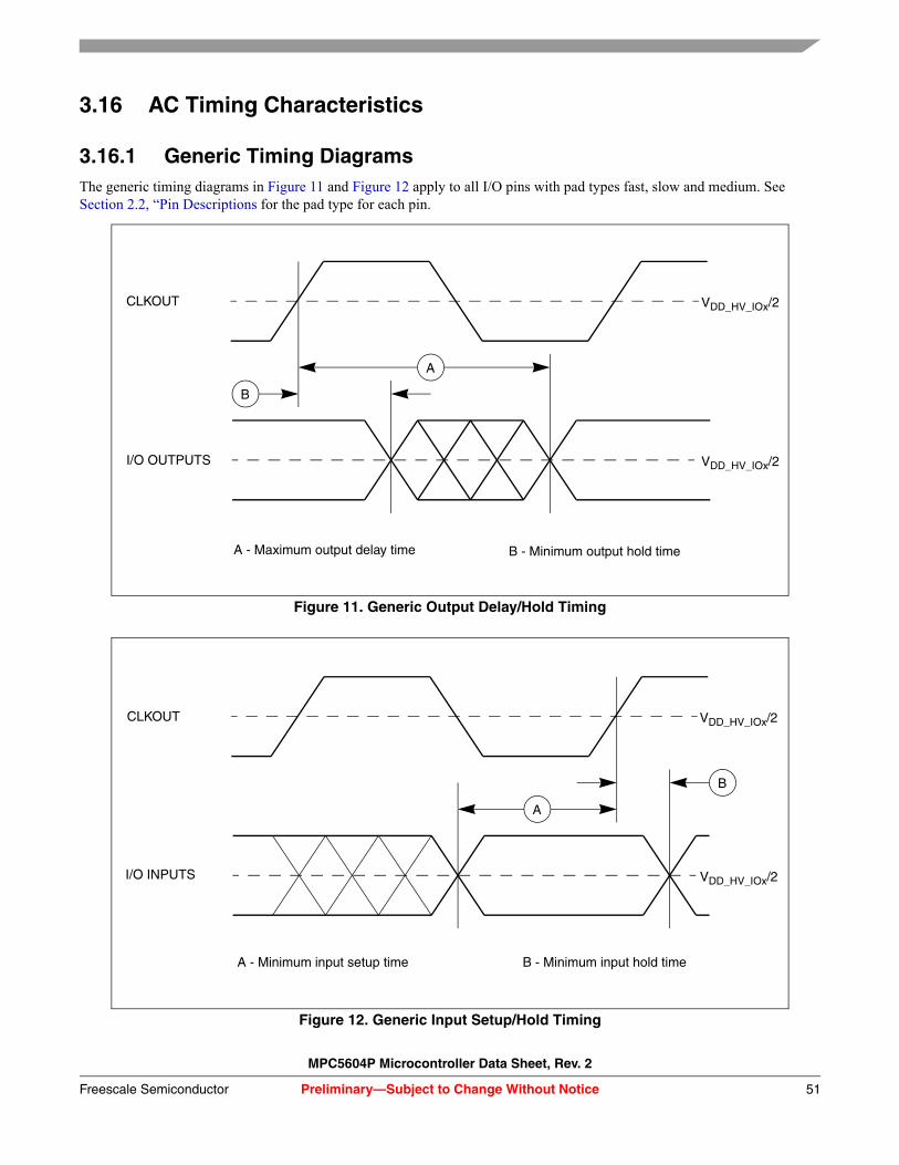
3.16 AC Timing Characteristics
3.16.1 Generic Timing DiagramsThe generic timing diagrams in Figure 11 and Figure 12 apply to all I/O pins with pad types fast, slow and medium. See Section 2.2, “Pin Descriptions for the pad type for each pin.
Figure 11. Generic Output Delay/Hold Timing
Figure 12. Generic Input Setup/Hold Timing
VDD_HV_IOx/2CLKOUT
A - Maximum output delay time B - Minimum output hold time
VDD_HV_IOx/2
A
B
I/O OUTPUTS
VDD_HV_IOx/2
A
B
CLKOUT
VDD_HV_IOx/2I/O INPUTS
A - Minimum input setup time B - Minimum input hold time
MPC5604P Microcontroller Data Sheet, Rev. 2
Preliminary—Subject to Change Without NoticeFreescale Semiconductor 51

3.16.2 RESET_B Pin CharacteristicsTable 33 gives the RESET_B pin characteristics at 5 V (4.5 V < VDD_HV_IOx < 5.5 V, NVUSRO[PAD3V5V]=0) operation.
Table 34 gives the RESET_B pin characteristics at 3.3 V (3.0 V < VDD_HV_IOx < 3.6 V, NVUSRO[PAD3V5V]=1) operation.
Table 33. RESET_B Pin1 Characteristics (5.0 V, NVUSRO[PAD3V5V]=0)
1 The RESET_B pin is weak pull-up during reset.
No. Symbol Parameter Conditions Min Max Unit
1 WFRST SR RESET pulse is sure to be filtered2
2 Pulse in between 70 ns and 500 ns may be either filtered or provided.
VDD=VDD_LV_CORx — 40 ns
2 WNFRST SR RESET pulse is sure not to be filtered VDD=VDD_LV_CORx 500 — ns
3 tPLH CC
AC
inpu
t
Propagation delay on rising edge Input slope = 15 ns
0.8 7 ns
Input slope = 5 ns 0.8 7
Input slope = 2 ns 0.6 7
4 tPHL CC Propagation delay on falling edge Input slope = 15 ns
0.8 7 ns
Input slope = 5 ns 0.8 7
Input slope = 2 ns 0.6 7
5 fmax SR Frequency of operation Input slope = 15 ns
— 25 MHz
Input slope = 5 ns — 50
Input slope = 2 ns — 100
6 tDC SR Duty cycle 40 60 %
7 tpd CC
AC
out
put
Propagation delay from VDD_HV_IOx/2 of internal signal to Nchannel switch on condition
Load = 25 pF 1 15 ns
Load = 50 pF 1 15
8 tSHL CC Slope at falling edge Load = 25 pF 1 8 ns
Load = 50 pF 2 15
9 ΔItr CC Current slew rate at rising edge of current Load = 25 pF 3 50 mA/ns
Load = 50 pF 3 50
Table 34. RESET_B Pin1 Characteristics (3.3 V, INVUSRO[PAD3V5V]=1)
No. Symbol Parameter Conditions Min Max Unit
1 WFRST SR RESET pulse is sure to be filtered — 40 ns
2 WNFRST SR RESET pulse is sure not to be filtered 500 — ns
MPC5604P Microcontroller Data Sheet, Rev. 2
Preliminary—Subject to Change Without Notice Freescale Semiconductor52

Figure 13. RESET_B pin
3 tPLH CC
AC
inpu
t
Propagation delay on rising edge Input slope = 15 ns 0.7 7 ns
Input slope = 5 ns 0.7 7
Input slope = 2 ns 0.7 7
4 tPHL CC Propagation delay on falling edge Input slope = 15 ns 0.7 7 ns
Input slope = 5 ns 0.7 7
Input slope = 2 ns 0.7 7
5 fmax SR Maximum frequency of operation Input slope = 15 ns — 25 MHz
Input slope = 5 ns — 50
Input slope = 2 ns — 100
6 tDC SR Duty cycle 40 60 %
7 tpd CC
AC
out
put
Propagation delay from VDD/2 of internal signal to Nchannel switch on condition
Load = 25 pF 1 20 ns
Load = 50 pF 1 20
8 tSHL CC Slope at falling edge Load = 25 pF 1 8 ns
Load = 50 pF 2 15
9 ΔItr CC Current slew rate at rising edge of current Load = 25 pF 2 60 mA/ns
Load = 50 pF 2 60
1 The RESET_B pin is weak pull-up during reset.
Table 34. RESET_B Pin1 Characteristics (3.3 V, INVUSRO[PAD3V5V]=1) (continued)
No. Symbol Parameter Conditions Min Max Unit
CLKOUT
4
2
1
RESET_B
MPC5604P Microcontroller Data Sheet, Rev. 2
Preliminary—Subject to Change Without NoticeFreescale Semiconductor 53

3.16.3 IEEE 1149.1 Interface Timing
Figure 14. JTAG test Clock input Timing
Table 35. JTAG Pin AC Electrical Characteristics
No. Symbol Parameter Conditions Min Max Unit
1 tJCYC CC TCK cycle time 100 — ns
2 tJDC CC TCK clock pulse width (measured at VDD_HV_IOx/2) 40 60 ns
3 tTCKRISE CC TCK rise and fall times (40% - 70%) — 3 ns
4 tTMSS, tTDIS CC TMS, TDI data setup time 5 — ns
5 tTMSH, tTDIH CC TMS, TDI data hold time 25 — ns
6 tTDOV CC TCK low to TDO data valid — 20 ns
7 tTDOI CC TCK low to TDO data invalid 0 — ns
8 tTDOHZ CC TCK low to TDO high impedance — 20 ns
11 tBSDV CC TCK falling edge to output valid — 50 ns
12 tBSDVZ CC TCK falling edge to output valid out of high impedance — 50 ns
13 tBSDHZ CC TCK falling edge to output high impedance — 50 ns
14 tBSDST CC Boundary scan input valid to TCK rising edge 50 — ns
15 tBSDHT CC TCK rising edge to boundary scan input invalid 50 — ns
TCK
1
2
2
3
3
MPC5604P Microcontroller Data Sheet, Rev. 2
Preliminary—Subject to Change Without Notice Freescale Semiconductor54

Figure 15. JTAG Test Access Port Timing
TCK
4
5
6
7 8
TMS, TDI
TDO
MPC5604P Microcontroller Data Sheet, Rev. 2
Preliminary—Subject to Change Without NoticeFreescale Semiconductor 55

Figure 16. JTAG Boundary Scan Timing
3.16.4 Nexus Timing
Table 36. Nexus Debug Port Timing1
No. Symbol Parameter Conditions Min Max Unit
1 tMCYC CC MCKO cycle time 2 8 tCYC
2 tMDC CC MCKO duty cycle 40 60 %
3 tMDOV CC MCKO low to MDO data valid2 - 0.1 0.2 tMCYC
4 tMSEOV CC MCKO low to MSEO data valid2 0.1 0.2 tMCYC
6 tEVTOV CC MCKO low to EVTO data valid2 - 0.1 0.2 tMCYC
7 tEVTIPW CC EVTI pulse width 4.0 — tTCYC
8 tEVTOPW CC EVTO pulse width 1 — tMCYC
TCK
OutputSignals
InputSignals
OutputSignals
11
12
13
14
15
MPC5604P Microcontroller Data Sheet, Rev. 2
Preliminary—Subject to Change Without Notice Freescale Semiconductor56

Figure 17. Nexus Output Timing
Figure 18. Nexus Event Trigger and Test Clock Timings
9 tTCYC CC TCK cycle time 43 — tCYC
10 tTDC CC TCK duty cycle 40 60 %
11 tNTDIS CC TDI data setup time 5 — ns
12 tNTDIH CC TDI data hold time 25 — ns
13 tNTMSS CC TMS data setup time 5 — ns
14 tNTMSH CC TMS data hold time 25 — ns
15 tJOV CC TCK low to TDO data valid 10 20 ns
16 — CC RDY valid to MCKO4 — — —
1 All Nexus timing relative to MCKO is measured from 50% of MCKO and 50% of the respective signal. 2 MDO, MSEO, and EVTO data is held valid until next MCKO low cycle.3 Lower frequency is required to be fully compliant to standard.4 The RDY pin timing is asynchronous to MCKO. The timing is guaranteed by design to function correctly.
Table 36. Nexus Debug Port Timing1 (continued)
No. Symbol Parameter Conditions Min Max Unit
1
2
4
6
MCKO
MDOMSEOEVTO
Output Data Valid
3
TCK
9 7
8
EVTIEVTO
8
7
MPC5604P Microcontroller Data Sheet, Rev. 2
Preliminary—Subject to Change Without NoticeFreescale Semiconductor 57

Figure 19. Nexus TDI, TMS, TDO Timing
3.16.5 External Interrupt Timing (IRQ pin)
Table 37. External Interrupt Timing1
1 IRQ timing specified at fSYS = 64 MHz and VDD_HV_IOx = 3.0 V to 5.5 V, TA = TL to TH, and CL = 200pF with SRC = 0b00.
No. Symbol Parameter Conditions Min Max Unit
1 tIPWL CC IRQ pulse width low 3 — tCYC
2 tIPWH CC IRQ pulse width high 3 — tCYC
3 tICYC CC IRQ edge to edge time2
2 Applies when IRQ pins are configured for rising edge or falling edge events, but not both.
6 — tCYC
TDO
13
14
TMS, TDI
15
TCK
12
11
MPC5604P Microcontroller Data Sheet, Rev. 2
Preliminary—Subject to Change Without Notice Freescale Semiconductor58

Figure 20. External Interrupt Timing
3.16.6 DSPI Timing
Table 38. DSPI Timing
No. Symbol Parameter Conditions Min Max Unit
1 tSCK CC DSPI cycle time Master (MTFE = 0) 62 — ns
Slave (MTFE = 0) 62 —
2 tCSC CC CS to SCK delay 16 — ns
3 tASC CC After SCK delay 16 — ns
4 tSDC CC SCK duty cycle 0.4 * tSCK 0.6 * tSCK ns
5 tA CC Slave access time SS active to SOUT valid — 40 ns
6 tDIS CC Slave SOUT disable time SS inactive to SOUT High-Z or invalid — 10 ns
7 tPCSC CC PCSx to PCSS time 13 — ns
8 tPASC CC PCSS to PCSx time 13 — ns
9 tSUI CC Data setup time for inputs Master (MTFE = 0) 20 — ns
Slave 2 —
Master (MTFE = 1, CPHA = 0) 5 —
Master (MTFE = 1, CPHA = 1) 20 —
10 tHI CC Data hold time for inputs Master (MTFE = 0) -5 — ns
Slave 4 —
Master (MTFE = 1, CPHA = 0) 11 —
Master (MTFE = 1, CPHA = 1) -5 —
IRQ
2
3
1
MPC5604P Microcontroller Data Sheet, Rev. 2
Preliminary—Subject to Change Without NoticeFreescale Semiconductor 59

Figure 21. DSPI Classic SPI Timing - Master, CPHA = 0
11 tSUO CC Data valid (after SCK edge) Master (MTFE = 0) — 4 ns
Slave — 23
Master (MTFE = 1, CPHA = 0) — 12
Master (MTFE = 1, CPHA = 1) — 4
12 tHO CC Data hold time for outputs Master (MTFE = 0) -2 — ns
Slave 6 —
Master (MTFE = 1, CPHA = 0) 6 —
Master (MTFE = 1, CPHA = 1) -2 —
Table 38. DSPI Timing (continued)
No. Symbol Parameter Conditions Min Max Unit
Data Last DataFirst Data
First Data Data Last Data
SIN
SOUT
PCSx
SCK Output
4
9
12
1
11
10
4
SCK Output
(CPOL=0)
(CPOL=1)
32
MPC5604P Microcontroller Data Sheet, Rev. 2
Preliminary—Subject to Change Without Notice Freescale Semiconductor60

Figure 22. DSPI Classic SPI Timing - Master, CPHA = 1
Figure 23. DSPI Classic SPI Timing - Slave, CPHA = 0
Data Last DataFirst DataSIN
SOUT
12 11
10
Last DataDataFirst Data
SCK Output
SCK Output
PCSx
9
(CPOL=0)
(CPOL=1)
Last DataFirst Data
3
4
1
Data
Data
SIN
SOUT
SS
4
5 6
9
11
10
12
SCK Input
First Data Last Data
SCK Input
2
(CPOL=0)
(CPOL=1)
MPC5604P Microcontroller Data Sheet, Rev. 2
Preliminary—Subject to Change Without NoticeFreescale Semiconductor 61

Figure 24. DSPI Classic SPI Timing - Slave, CPHA = 1
Figure 25. DSPI Modified Transfer Format Timing - Master, CPHA = 0
5 6
9
12
11
10
Last Data
Last DataSIN
SOUT
SS
First Data
First Data
Data
Data
SCK Input
SCK Input
(CPOL=0)
(CPOL=1)
PCSx
3
14
10
4
9
12 11
SCK Output
SCK Output
SIN
SOUT
First Data Data Last Data
First Data Data Last Data
2
(CPOL=0)
(CPOL=1)
MPC5604P Microcontroller Data Sheet, Rev. 2
Preliminary—Subject to Change Without Notice Freescale Semiconductor62

Figure 26. DSPI Modified Transfer Format Timing - Master, CPHA = 1
Figure 27. DSPI Modified Transfer Format Timing - Slave, CPHA = 0
PCSx
109
12 11
SCK Output
SCK Output
SIN
SOUT
First Data Data Last Data
First Data Data Last Data
(CPOL=0)
(CPOL=1)
Last DataFirst Data
3
4
1
Data
Data
SIN
SOUT
SS
4
5 6
9
11
10
SCK Input
First Data Last Data
SCK Input
2
(CPOL=0)
(CPOL=1)
12
MPC5604P Microcontroller Data Sheet, Rev. 2
Preliminary—Subject to Change Without NoticeFreescale Semiconductor 63

Figure 28. DSPI Modified Transfer Format Timing - Slave, CPHA = 1
Figure 29. DSPI PCS Strobe (PCSS) Timing
5 6
9
12
11
10
Last Data
Last DataSIN
SOUT
SS
First Data
First Data
Data
Data
SCK Input
SCK Input
(CPOL=0)
(CPOL=1)
PCSx
7 8
PCSS
MPC5604P Microcontroller Data Sheet, Rev. 2
Preliminary—Subject to Change Without Notice Freescale Semiconductor64

4 Package Characteristics
4.1 Package Mechanical Data
4.1.1 144 LQFP Mechanical Outline Drawing
Figure 30. 144 LQFP Package Mechanical Drawing (part 1)
MPC5604P Microcontroller Data Sheet, Rev. 2
Preliminary—Subject to Change Without NoticeFreescale Semiconductor 65
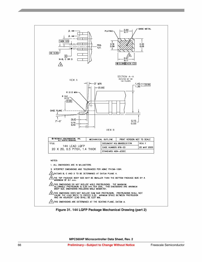
Figure 31. 144 LQFP Package Mechanical Drawing (part 2)
MPC5604P Microcontroller Data Sheet, Rev. 2
Preliminary—Subject to Change Without Notice Freescale Semiconductor66

4.1.2 100 LQFP Mechanical Outline Drawing
Figure 32. 100 LQFP Package Mechanical Drawing (part 1)
MPC5604P Microcontroller Data Sheet, Rev. 2
Preliminary—Subject to Change Without NoticeFreescale Semiconductor 67

Figure 33. 100 LQFP Package Mechanical Drawing (part 2)
MPC5604P Microcontroller Data Sheet, Rev. 2
Preliminary—Subject to Change Without Notice Freescale Semiconductor68

Figure 34. 100 LQFP Package Mechanical Drawing (part 3)
MPC5604P Microcontroller Data Sheet, Rev. 2
Preliminary—Subject to Change Without NoticeFreescale Semiconductor 69

5 Ordering InformationTable 39 shows the orderable part numbers for the MPC5604P series.
Figure 35. Commercial Product Code Structure
Table 39. Orderable Part Number Summary
Part Number Flash (KB) SRAM (KB) Package Characteristics
MPC5604PEFMLQ 576 40 144 LQFP Data flash; FlexRay
MPC5604PEFMLL 576 40 100 LQFP Data flash; FlexRay
MPC5603PEFMLQ 448 32 144 LQFP Data flash; FlexRay
MPC5603PEFMLL 448 32 100 LQFP Data flash; FlexRay
MPC5602PEFMLQ 320 24 144 LQFP Data flash; FlexRay
MPC5602PEFMLL 320 24 100 LQFP Data flash; FlexRay
Qualification Status
PowerPC Core
Automotive Platform
Core Version
Flash Size (core dependent)
Product
Optional fields
M PC 56 P E M LLExample code: 0 4
Temperature spec.
Package Code
Qualification StatusM = MC statusS = Auto qualifiedP = PC status
Automotive Platform56 = PPC in 90nm57 = PPC in 65nm
Core Version0 = e200z0
Flash Size (z0 core)2 = 320 KB3 = 448 KB4 = 576 KB
ProductP = PictusC = Gateway
Optional fieldsE = Data Flash (blank if none)
R = Tape & Reel (blank if Tray)
R
Temperature spec.V = –40°C to 105°CM = –40°C to 125°C
Package CodeLL = 100 LQFPLQ = 144 LQFP
MPC5604P Microcontroller Data Sheet, Rev. 2
Preliminary—Subject to Change Without Notice Freescale Semiconductor70

Revision Date Substantive changes
Rev. 1 8/2008 Initial release
Rev. 2 11/2008 Table 4:TDO and TDI pins (Port pins B[4:5] are single function pins.
Table 8, Table 9: Thermal characteristics added.
Table 10, Table 11:EMI testing specifications split into separate tables for Normal mode and Airbag mode; data to be added in a later revision.
Table 16, Table 17, Table 19, Table 20:Supply current specifications split into separate tables for Normal mode and Airbag mode; data to be added in a later revision.
Table 18: • Values for IOL and IOH (in Conditions column) changed.
• Max values for VOH_S, VOH_M, VOH_F and VOH_SYM deleted.
• VILR max value changed.• IPUR min and max values changed.
Table 21: Sensitivity value changed.
Table 32: Most values in table changed.
MPC5604P Microcontroller Data Sheet, Rev. 2
Preliminary—Subject to Change Without NoticeFreescale Semiconductor 71

How to Reach Us:
Home Page:www.freescale.com
Web Support:http://www.freescale.com/support
USA/Europe or Locations Not Listed:Freescale Semiconductor, Inc.Technical Information Center, EL5162100 East Elliot RoadTempe, Arizona 85284+1-800-521-6274 or +1-480-768-2130www.freescale.com/support
Europe, Middle East, and Africa:Freescale Halbleiter Deutschland GmbHTechnical Information CenterSchatzbogen 781829 Muenchen, Germany+44 1296 380 456 (English)+46 8 52200080 (English)+49 89 92103 559 (German)+33 1 69 35 48 48 (French)www.freescale.com/support
Japan:Freescale Semiconductor Japan Ltd.HeadquartersARCO Tower 15F1-8-1, Shimo-Meguro, Meguro-ku,Tokyo 153-0064Japan0120 191014 or +81 3 5437 [email protected]
Asia/Pacific:Freescale Semiconductor China Ltd.Exchange Building 23FNo. 118 Jianguo RoadChaoyang DistrictBeijing 100022 China +86 10 5879 [email protected]
For Literature Requests Only:Freescale Semiconductor Literature Distribution CenterP.O. Box 5405Denver, Colorado 802171-800-441-2447 or 303-675-2140Fax: [email protected]
Document Number: MPC5604PRev. 2November 2008
Information in this document is provided solely to enable system and software implementers to use Freescale Semiconductor products. There are no express or implied copyright licenses granted hereunder to design or fabricate any integrated circuits or integrated circuits based on the information in this document.
Freescale Semiconductor reserves the right to make changes without further notice to any products herein. Freescale Semiconductor makes no warranty, representation or guarantee regarding the suitability of its products for any particular purpose, nor does Freescale Semiconductor assume any liability arising out of the application or use of any product or circuit, and specifically disclaims any and all liability, including without limitation consequential or incidental damages. “Typical” parameters that may be provided in Freescale Semiconductor data sheets and/or specifications can and do vary in different applications and actual performance may vary over time. All operating parameters, including “Typicals”, must be validated for each customer application by customer’s technical experts. Freescale Semiconductor does not convey any license under its patent rights nor the rights of others. Freescale Semiconductor products are not designed, intended, or authorized for use as components in systems intended for surgical implant into the body, or other applications intended to support or sustain life, or for any other application in which the failure of the Freescale Semiconductor product could create a situation where personal injury or death may occur. Should Buyer purchase or use Freescale Semiconductor products for any such unintended or unauthorized application, Buyer shall indemnify and hold Freescale Semiconductor and its officers, employees, subsidiaries, affiliates, and distributors harmless against all claims, costs, damages, and expenses, and reasonable attorney fees arising out of, directly or indirectly, any claim of personal injury or death associated with such unintended or unauthorized use, even if such claim alleges that Freescale Semiconductor was negligent regarding the design or manufacture of the part.
Freescale™ and the Freescale logo are trademarks of Freescale Semiconductor, Inc. All other product or service names are the propertyof their respective owners. The ARM POWERED logo is a registered trademark of ARM Limited. ARM7TDMI-S is a trademark of ARM Limited. Java and all other Java-based marks are trademarks or registered trademarks of Sun Microsystems, Inc. in the U.S. and other countries.The Bluetooth trademarks are owned by their proprietor and used by Freescale Semiconductor, Inc. under license.
© Freescale Semiconductor, Inc. 2008. All rights reserved.
MPC5604P Microcontroller Data Sheet, Rev. 2
Preliminary—Subject to Change Without Notice Freescale Semiconductor72