Fourth GenerationFourth Generation Photovoltaics Research ... · PDF fileFourth...
101
Fourth Generation Fourth Generation Photovoltaics Research in India Vikram Kumar Physics / CARE / NRF Indian Institute of Technology Delhi [email protected]
Transcript of Fourth GenerationFourth Generation Photovoltaics Research ... · PDF fileFourth...
Fourth GenerationFourth Generation Photovoltaics Research in
India
Vikram Kumar Physics / CARE / NRFy
Indian Institute of Technology [email protected]
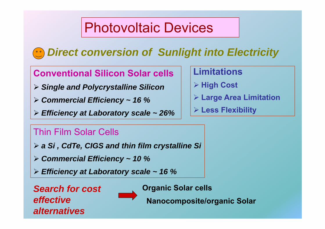
Photovoltaic Devices
Direct conversion of Sunlight into Electricity
Conventional Silicon Solar cellsSingle and Polycrystalline Silicon
LimitationsHigh CostSingle and Polycrystalline Silicon
Commercial Efficiency ~ 16 %Efficiency at Laboratory scale ~ 26%
gLarge Area LimitationLess FlexibilityEfficiency at Laboratory scale 26%
Thin Film Solar Cellsa Si , CdTe, CIGS and thin film crystalline SiCommercial Efficiency ~ 10 %Efficiency at Laboratory scale ~ 16 %
Search for cost Organic Solar cells effective alternatives
Nanocomposite/organic Solar
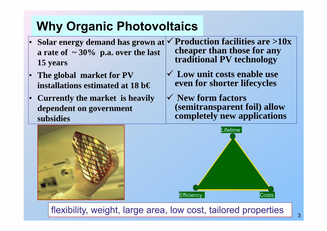
Why Organic Photovoltaics• Solar energy demand has grown at
a rate of ~ 30% p.a. over the last 15 years
Production facilities are >10x cheaper than those for any traditional PV technology15 years
• The global market for PV installations estimated at 18 b€
gyLow unit costs enable use even for shorter lifecycles
• Currently the market is heavily dependent on government
i i
New form factors (semitransparent foil) allow completely new applicationssubsidies completely new applications
Lifetime
CostsEfficiency
3flexibility, weight, large area, low cost, tailored properties
CostsEfficiency
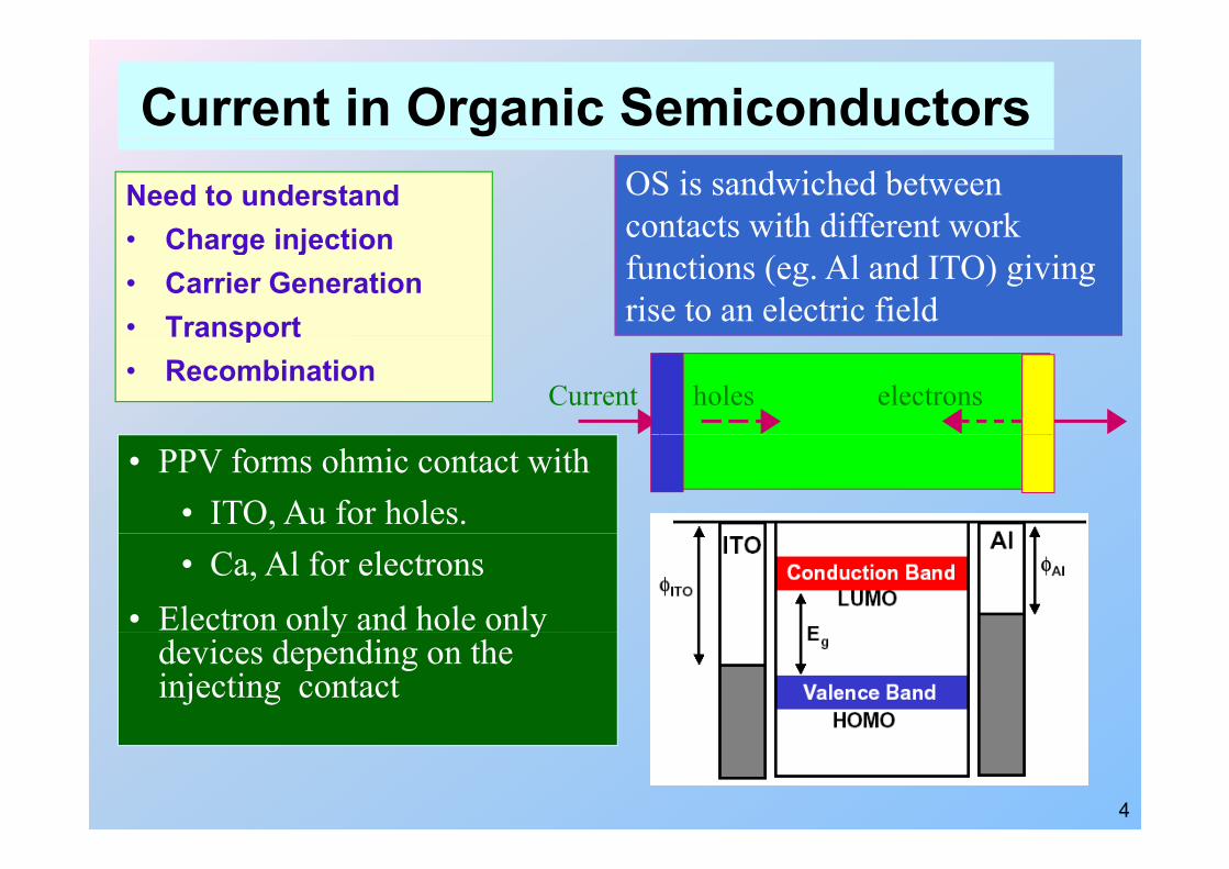
Current in Organic SemiconductorsNeed to understand• Charge injection
OS is sandwiched between contacts with different work • Charge injection
• Carrier Generation• Transport
functions (eg. Al and ITO) giving rise to an electric field Transport
• RecombinationCurrent holes electrons
• PPV forms ohmic contact with • ITO, Au for holes.• Ca, Al for electrons
• Electron only and hole only y ydevices depending on the injecting contact
4
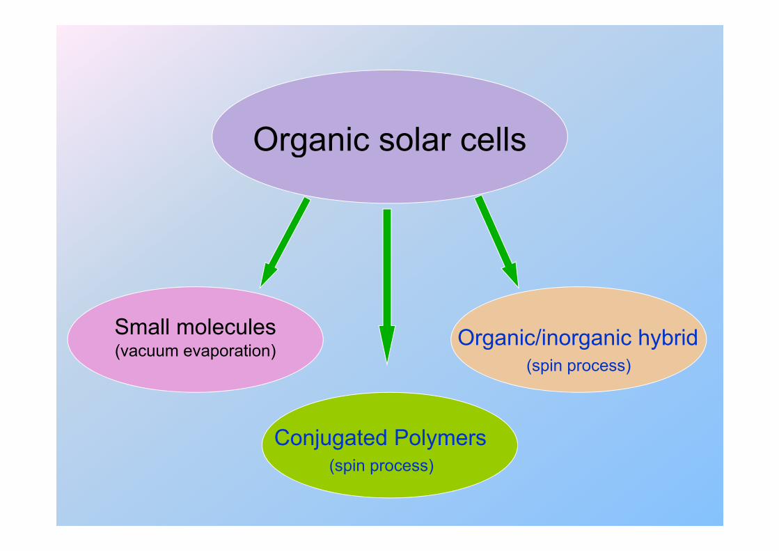
Organic solar cellsOrganic solar cells
Small molecules Organic/inorganic hybrid(vacuum evaporation)
Organic/inorganic hybrid(spin process)
Conjugated Polymers(spin process)(spin process)
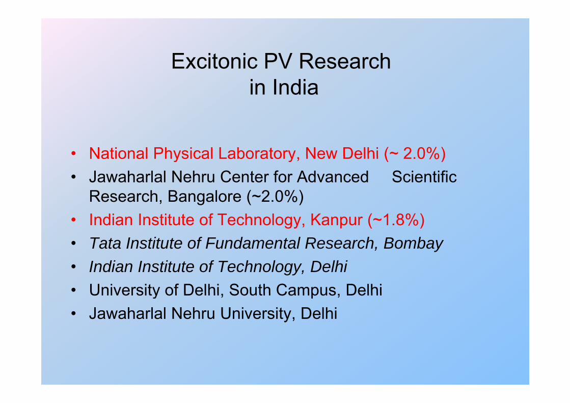
Excitonic PV ResearchExcitonic PV Researchin India
• National Physical Laboratory New Delhi (~ 2 0%)National Physical Laboratory, New Delhi ( 2.0%)• Jawaharlal Nehru Center for Advanced Scientific
Research, Bangalore (~2.0%)Research, Bangalore ( 2.0%) • Indian Institute of Technology, Kanpur (~1.8%)• Tata Institute of Fundamental Research, BombayTata Institute of Fundamental Research, Bombay• Indian Institute of Technology, Delhi• University of Delhi South Campus DelhiUniversity of Delhi, South Campus, Delhi• Jawaharlal Nehru University, Delhi
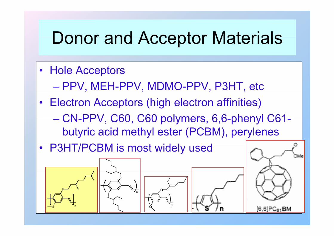
Donor and Acceptor MaterialsDonor and Acceptor Materials
• Hole Acceptors– PPV, MEH-PPV, MDMO-PPV, P3HT, etc, , , ,
• Electron Acceptors (high electron affinities)CN PPV C60 C60 polymers 6 6 phenyl C61– CN-PPV, C60, C60 polymers, 6,6-phenyl C61-butyric acid methyl ester (PCBM), perylenes
P3HT/PCBM i t id l d• P3HT/PCBM is most widely used
n
O
O
O
O n
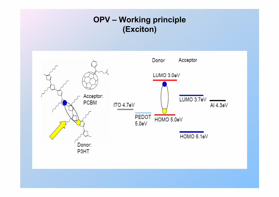
OPV – Working principle (Exciton)(Exciton)
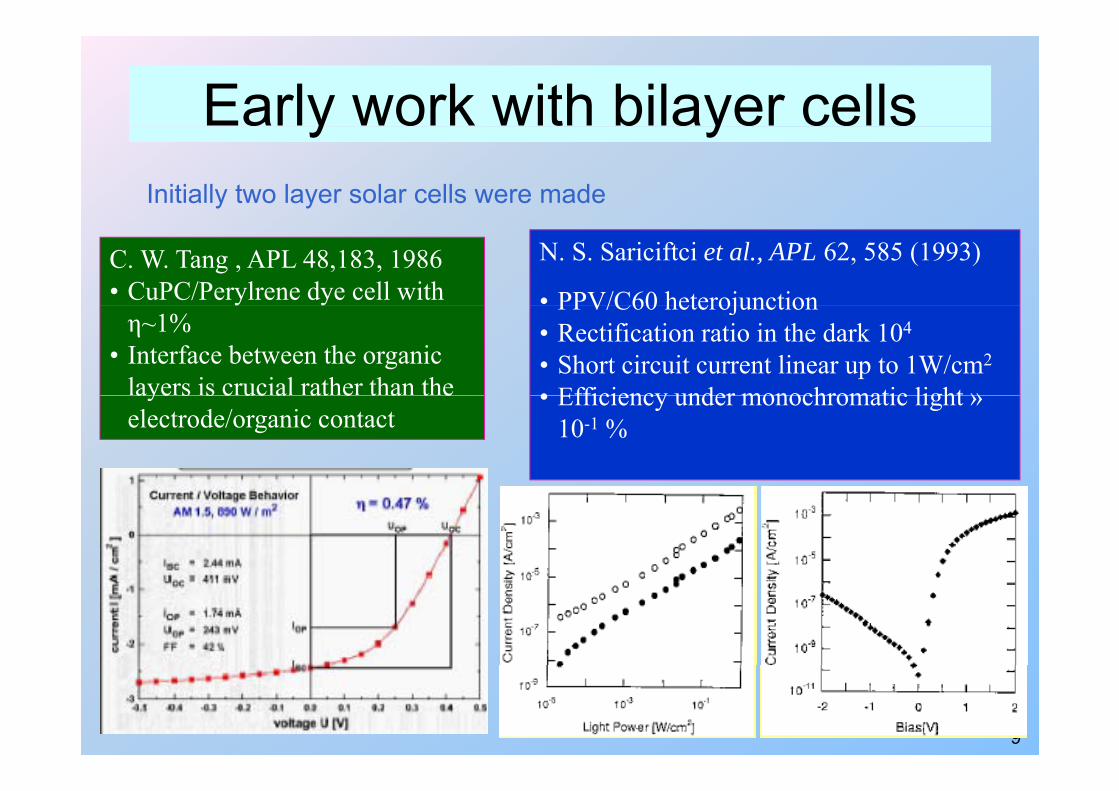
Early work with bilayer cellsy yInitially two layer solar cells were made
C. W. Tang , APL 48,183, 1986• CuPC/Perylrene dye cell with
N. S. Sariciftci et al., APL 62, 585 (1993)
• PPV/C60 heterojunctionη~1%
• Interface between the organic layers is crucial rather than the
PPV/C60 heterojunction• Rectification ratio in the dark 104
• Short circuit current linear up to 1W/cm2
• Efficiency under monochromatic light »aye s s c uc a at e t a t eelectrode/organic contact
• Efficiency under monochromatic light » 10-1 %
9
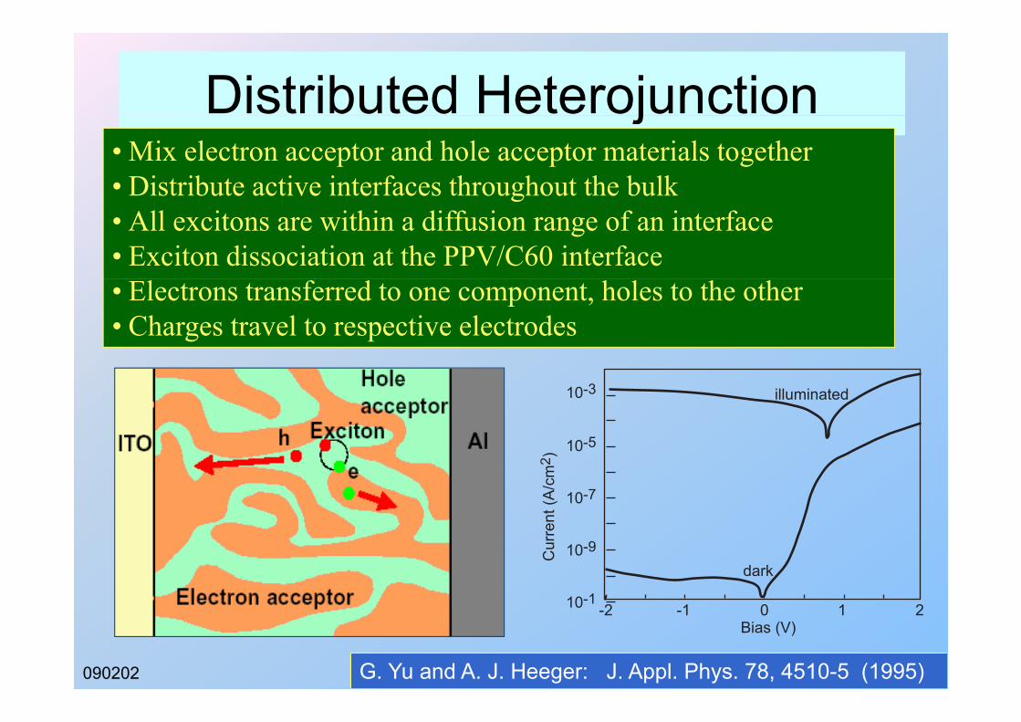
Distributed Heterojunctionj• Mix electron acceptor and hole acceptor materials together• Distribute active interfaces throughout the bulkg• All excitons are within a diffusion range of an interface• Exciton dissociation at the PPV/C60 interface• Electrons transferred to one component, holes to the other• Charges travel to respective electrodes
����
����
���������
��
���
�� �
����
����
� � � � �
���
�����
����
����
090202 10
�� �� � � ������ ��
��
G. Yu and A. J. Heeger: J. Appl. Phys. 78, 4510-5 (1995)
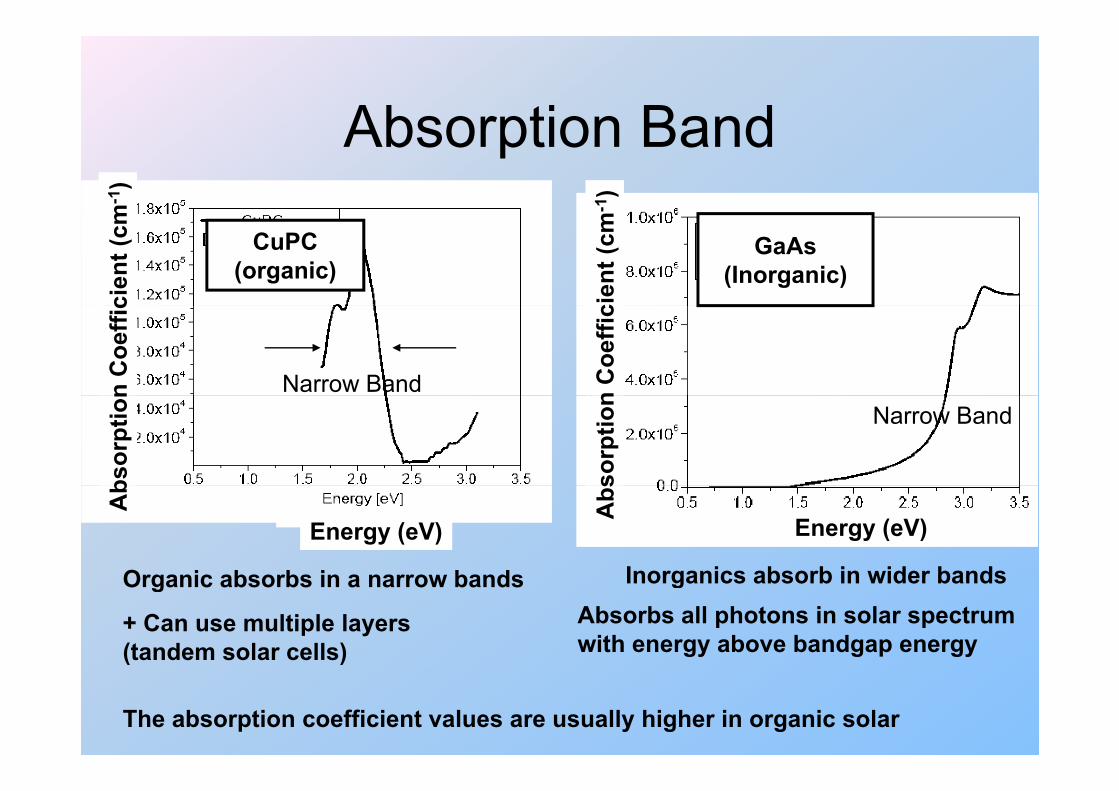
Absorption BandAbsorption Band
m-1
)
m-1
)
cien
t (cm GaAs
(Inorganic)
cien
t (cm CuPC
(organic)
n C
oeffi
c
n C
oeffi
c
Narrow Band
sorp
tion
bsor
ptio
n
Narrow Band
Abs
Energy (eV)Energy (eV)
Energy (eV)
Ab
Organic absorbs in a narrow bands Inorganics absorb in wider bandsOrganic absorbs in a narrow bands Inorganics absorb in wider bands
+ Can use multiple layers(tandem solar cells)
Absorbs all photons in solar spectrumwith energy above bandgap energy( )
The absorption coefficient values are usually higher in organic solar
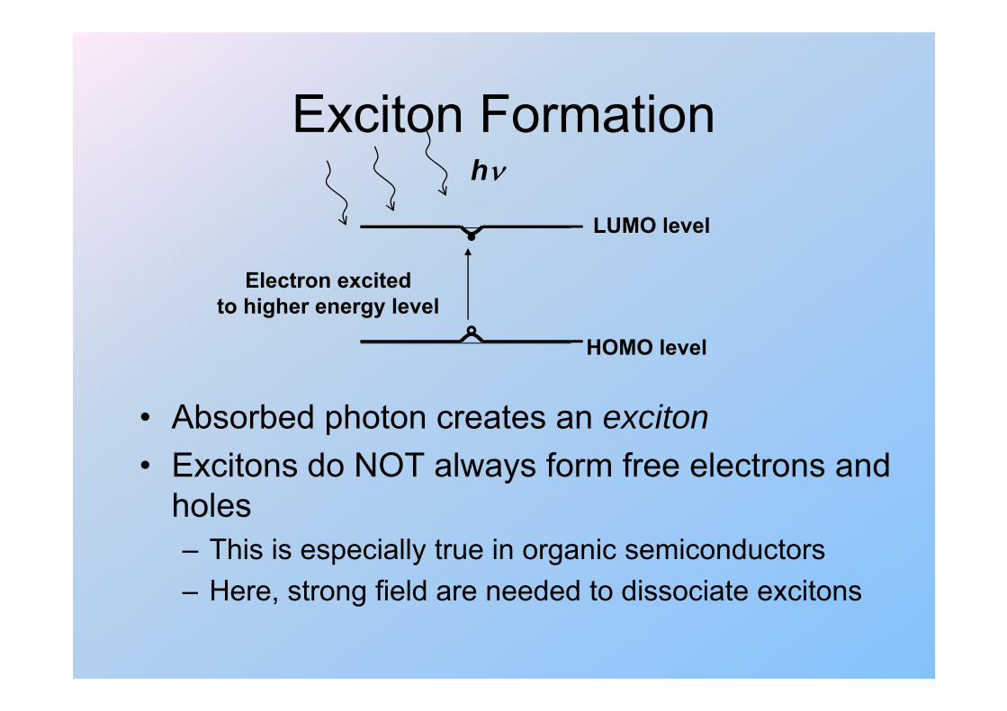
Exciton FormationExciton Formationhν
LUMO level
El t it d
HOMO level
Electron excitedto higher energy level
• Absorbed photon creates an exciton• Excitons do NOT always form free electrons and
holes o es– This is especially true in organic semiconductors– Here, strong field are needed to dissociate excitonsHere, strong field are needed to dissociate excitons

Photovoltaic Process In Organic Solar gCells
Coupling Absorption Creation Separation CollectionCreationht
of sunlightinto
solar cell
of incidentphotons
of ‘free’ charges
of chargesby built-inE field
of chargesat
electrodes
Creationof
excitonsSunl
ig
Li ht Ph tLightReflected
Away
PhotonsNot
Absorbed
ChargesRecombine
ChargesRecombine
ExcitonsRecombine
Efficiency of this step is ~100%for inorganic solar cells

Built in FieldBuilt-in Field
φbiEf φbi
Eb ilt i n-typep-type Ebuilt-in
Ebuilt-in
O i M t i lOrganicMaterial Inorganic semiconductord
No charge of its ownBuilt-in potential depends on electrode work function difference

In Typical OSCIn Typical OSCOSC is typically different from inorganic solar cells in the following ways:
• Absorption in a narrower spectral bandAbsorption in a narrower spectral band
• Usually high absorption coefficienty g p
• Exciton binding energy higherg gy g
• Poor charge mobilityg y
• Built-in potential dependent on electrodes
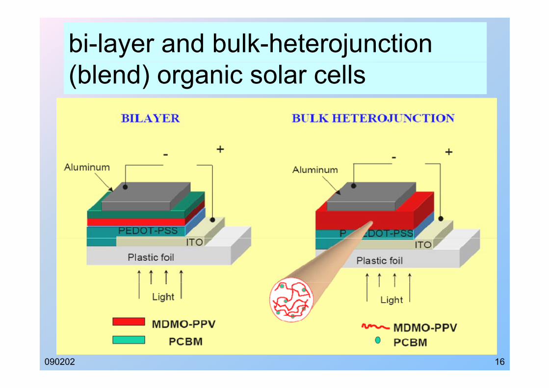
bi-layer and bulk-heterojunction (blend) organic solar cells
090202 16
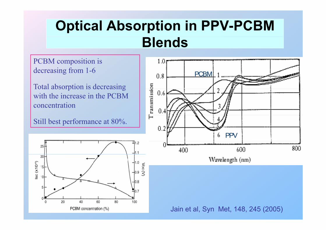
Optical Absorption in PPV-PCBM Blends
PCBM composition isPCBM composition is decreasing from 1-6
Total absorption is decreasing
PCBM
Total absorption is decreasing with the increase in the PCBM concentration
Still best performance at 80%.
PPV
Jain et al, Syn Met, 148, 245 (2005)
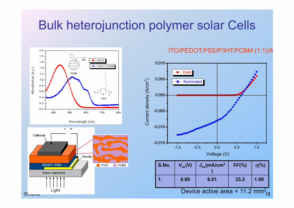
Bulk heterojunction polymer solar Cells
ITO/PEDOT:PSS/P3HT:PCBM (1:1)/A
0.005
0.010
0.005
0.010
Dark
2 )
Ill i t d
0.0000.000
nsity
(A/c
m2 Illuminated
-0 010
-0.005
-0 010
-0.005
Cur
rent
de
-1.0 -0.5 0.0 0.5 1.0-0.015
0.010
-0.015
0.010
S.No. Voc(V) Jsc(mA/cm2
)FF(%) η(%)
Voltage (V)
090202 18
1. 0.60 8.01 33.2 1.99
Device active area = 11.2 mm2
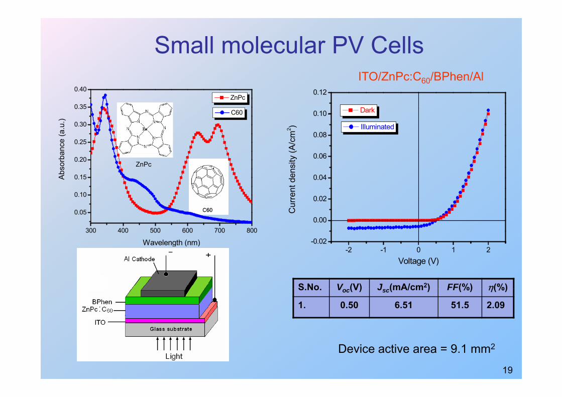
Small molecular PV Cells
0.12
D k
ITO/ZnPc:C60/BPhen/Al
0.35
0.40 ZnPc
0 06
0.08
0.10
(A/c
m2 ) Illuminated
Dark
0.25
0.30
0.35
ance
(a.u
.)
C60
0 02
0.04
0.06
rent
den
sity
ZnPc
0.10
0.15
0.20
Abso
rba
-0.02
0.00
0.02
Cur
r
0.05
300 400 500 600 700 800
Wavelength (nm)
S No V (V) J (mA/cm2) FF(%) η(%)
-2 -1 0 1 20.02
Voltage (V)
Wavelength (nm)
S.No. Voc(V) Jsc(mA/cm ) FF(%) η(%)
1. 0.50 6.51 51.5 2.09
19
Device active area = 9.1 mm2
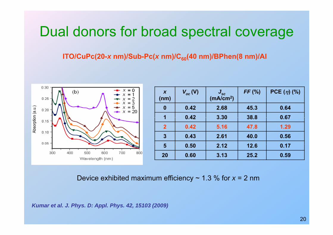
Dual donors for broad spectral coveragep gITO/CuPc(20-x nm)/Sub-Pc(x nm)/C60(40 nm)/BPhen(8 nm)/Al
x V (V) J FF (%) PCE ( ) (%)x(nm)
Voc (V) Jsc (mA/cm2)
FF (%) PCE (η) (%)
0 0.42 2.68 45.3 0.641 0 42 3 30 38 8 0 671 0.42 3.30 38.8 0.672 0.42 5.16 47.8 1.293 0.43 2.61 40.0 0.565 0 50 2 12 12 6 0 175 0.50 2.12 12.6 0.17
20 0.60 3.13 25.2 0.59
Device exhibited maximum efficiency ~ 1.3 % for x = 2 nm
20
Kumar et al. J. Phys. D: Appl. Phys. 42, 15103 (2009)
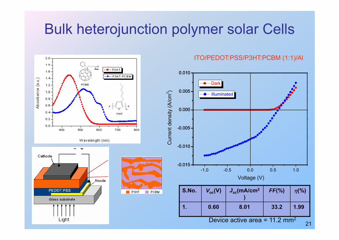
Bulk heterojunction polymer solar Cells
ITO/PEDOT:PSS/P3HT:PCBM (1:1)/Al
0.005
0.010
0.005
0.010
Dark
2 )
Ill i t d
0.0000.000
nsity
(A/c
m2 Illuminated
-0 010
-0.005
-0 010
-0.005
Cur
rent
de
-1.0 -0.5 0.0 0.5 1.0-0.015
0.010
-0.015
0.010
S.No. Voc(V) Jsc(mA/cm2
)FF(%) η(%)
Voltage (V)
21
1. 0.60 8.01 33.2 1.99
Device active area = 11.2 mm2
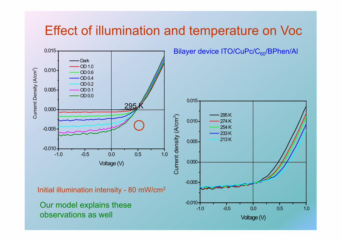
Effect of illumination and temperature on Voc0.015
Dark OD 1 0
Bilayer device ITO/CuPc/C60/BPhen/Al
0.005
0.010
nsity
(A/c
m2 ) OD 1.0
OD 0.6 OD 0.4 OD 0.2 OD 0.1
0.000
Cur
rem
t Den OD 0.0
0010
0.015
m2 ) 295 K
274 K
295 K
0 010
-0.005
0.005
0.010
ensi
ty (A
/cm 274 K
254 K 233 K 213 K
-1.0 -0.5 0.0 0.5 1.0-0.010
Voltage (V) 0.000
Cur
rent
de
0 010
-0.005
O d l l i th
Initial illumination intensity - 80 mW/cm2
-1.0 -0.5 0.0 0.5 1.0-0.010
Voltage (V)
Our model explains these observations as well

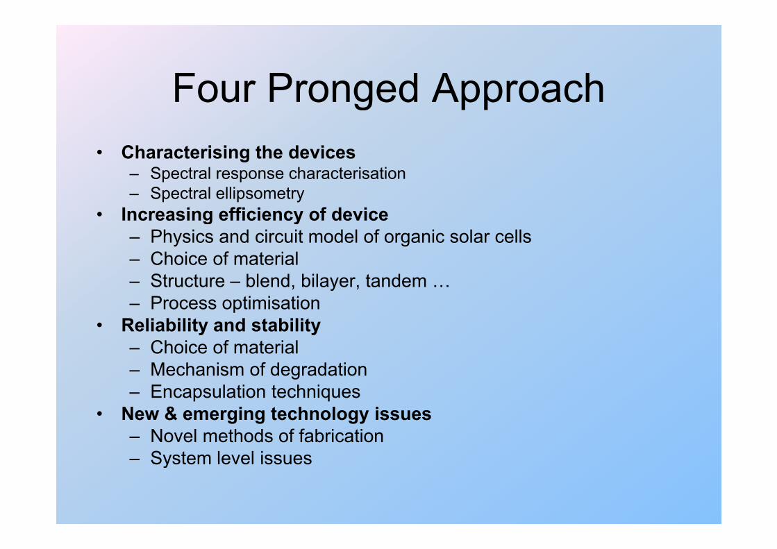
Four Pronged ApproachFour Pronged Approach• Characterising the devices• Characterising the devices
– Spectral response characterisation– Spectral ellipsometry
• Increasing efficiency of device• Increasing efficiency of device– Physics and circuit model of organic solar cells– Choice of material
St t bl d bil t d– Structure – blend, bilayer, tandem …– Process optimisation
• Reliability and stability– Choice of material– Mechanism of degradation– Encapsulation techniquesp q
• New & emerging technology issues– Novel methods of fabrication– System level issuesSystem level issues

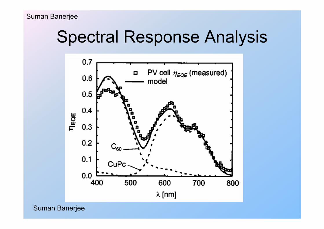
Spectral Response AnalysisSuman Banerjee
Spectral Response Analysis
Suman Banerjee
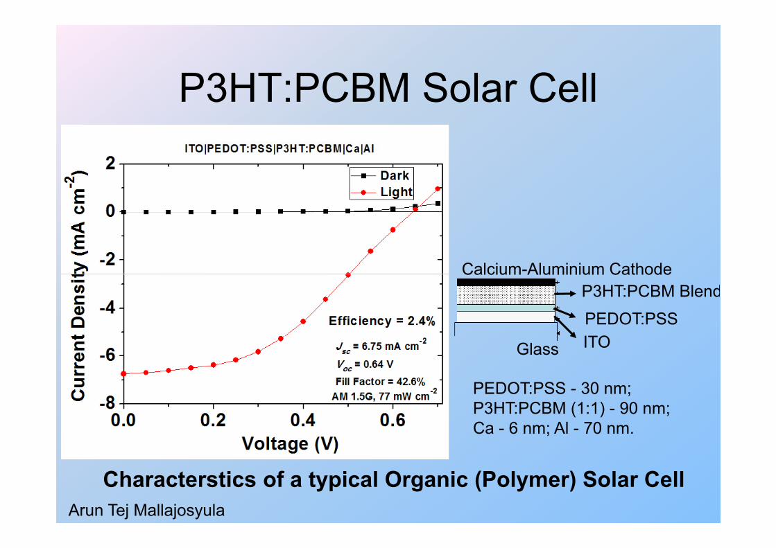
P3HT:PCBM Solar CellP3HT:PCBM Solar Cell
Calcium-Aluminium CathodeCalcium Aluminium CathodeP3HT:PCBM Blend
PEDOT:PSS ITO
PEDOT:PSS - 30 nm;
ITO Glass
P3HT:PCBM (1:1) - 90 nm; Ca - 6 nm; Al - 70 nm.
Characterstics of a typical Organic (Polymer) Solar CellArun Tej Mallajosyula
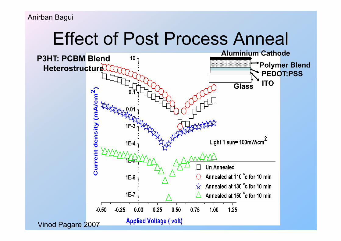
Effect of Post Process AnnealAnirban Bagui
Effect of Post Process AnnealP3HT: PCBM Blend
H t t t
Aluminium CathodePolymer BlendHeterostructure Polymer Blend PEDOT:PSS ITO Glass
Vinod Pagare 2007
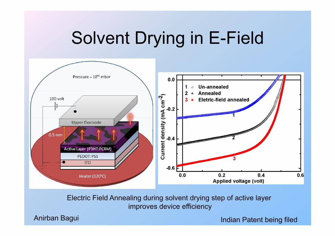
Solvent Drying in E FieldSolvent Drying in E-Field
Electric Field Annealing during solvent drying step of active layerElectric Field Annealing during solvent drying step of active layer improves device efficiency
Anirban Bagui Indian Patent being filed

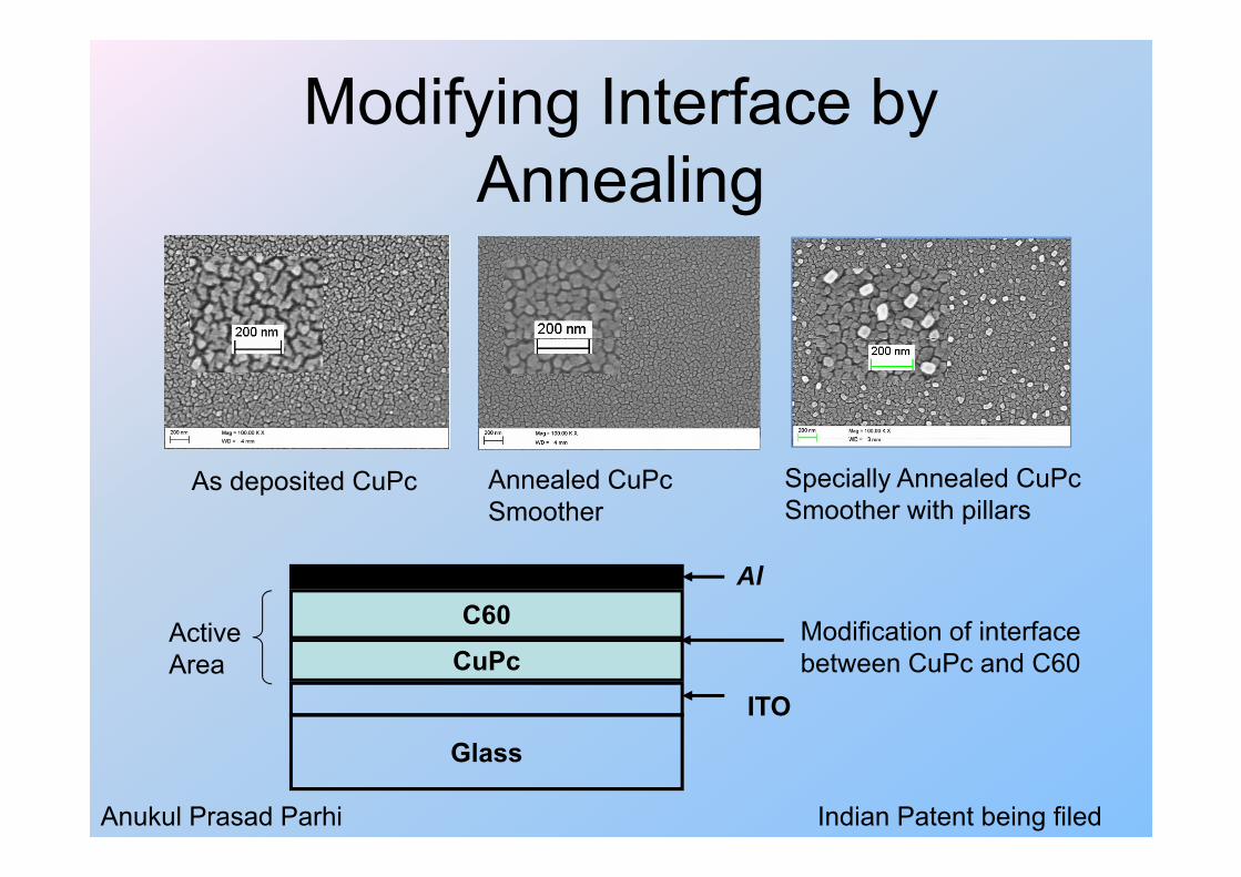
Modifying Interface by Annealing
As deposited CuPc Annealed CuPcSmoother
Specially Annealed CuPcSmoother with pillars
C60Al
Modification of interfaceActive
ITOCuPc
Modification of interfacebetween CuPc and C60
ActiveArea
Glass
Anukul Prasad Parhi Indian Patent being filed
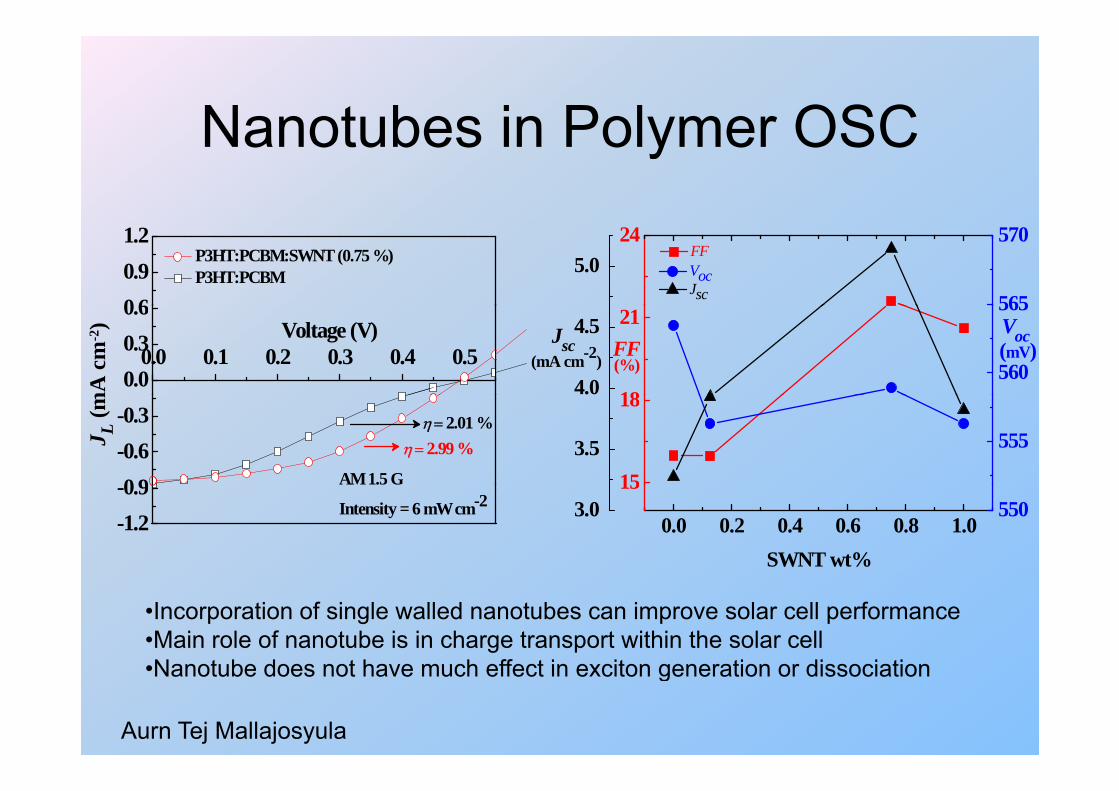
Nanotubes in Polymer OSCNanotubes in Polymer OSC
0 60.91.2
P3HT:PCBM:SWNT (0.75 %) P3HT:PCBM
24
FF
565
570 Voc5.0 Jsc
0.0 0.1 0.2 0.3 0.4 0.50.00.30.6
mA
cm
-2) Voltage (V)
18
21
560
565
4.0
4.5Jsc Voc
FF(%)
(mV)(mA cm-2)
0 9-0.6-0.3
η = 2.99 %η = 2.01 %
J L (m
AM 1.5 G 15
18
5553.5
-1.2-0.9
Intensity = 6 mW cm-20.0 0.2 0.4 0.6 0.8 1.0
15
SWNT wt%
5503.0
•Incorporation of single walled nanotubes can improve solar cell performance•Main role of nanotube is in charge transport within the solar cellNanotube does not have much effect in exciton generation or dissociation•Nanotube does not have much effect in exciton generation or dissociation
Aurn Tej Mallajosyula

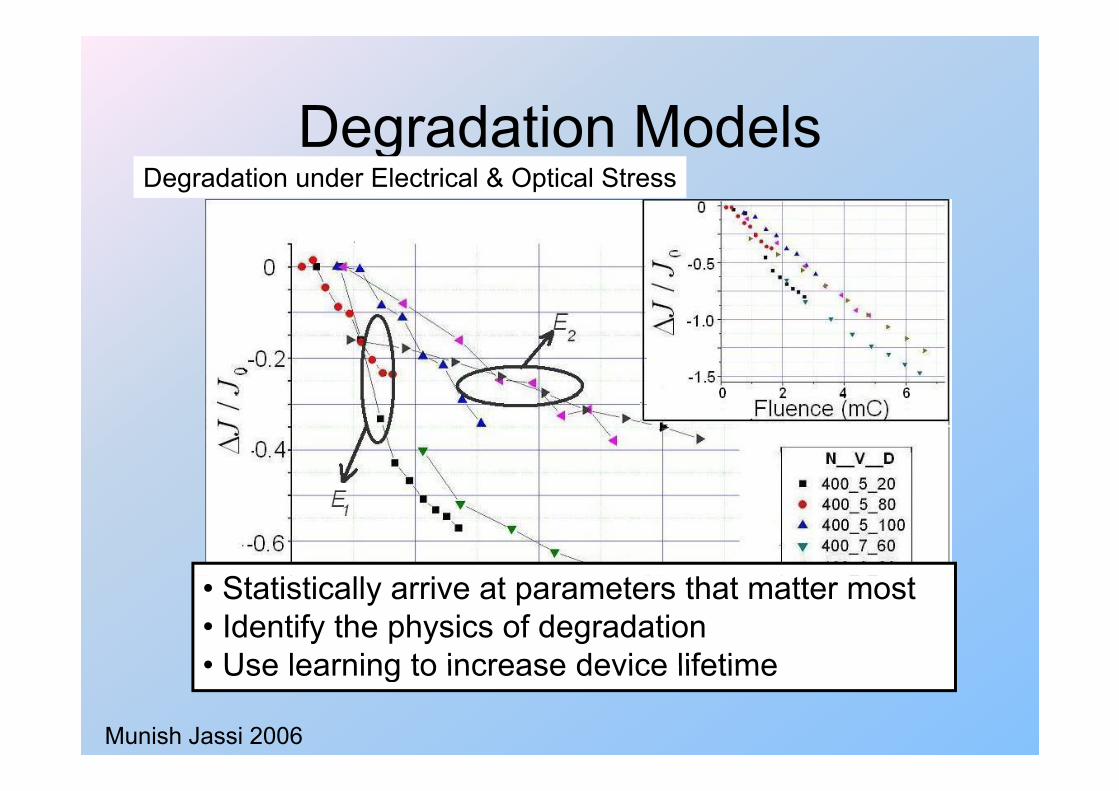
Degradation ModelsDegradation ModelsDegradation under Electrical & Optical Stress
• Statistically arrive at parameters that matter most• Identify the physics of degradation• Use learning to increase device lifetime
Munish Jassi 2006
• Use learning to increase device lifetime
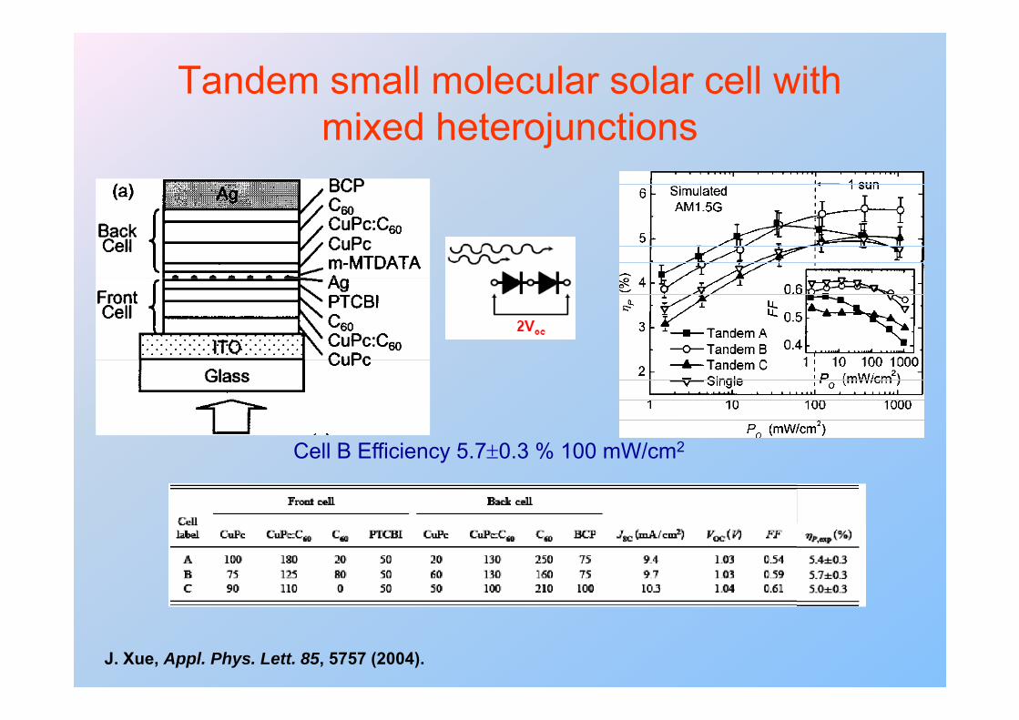
Tandem small molecular solar cell with i d h t j timixed heterojunctions
2Cell B Efficiency 5.7±0.3 % 100 mW/cm2
J. Xue, Appl. Phys. Lett. 85, 5757 (2004).
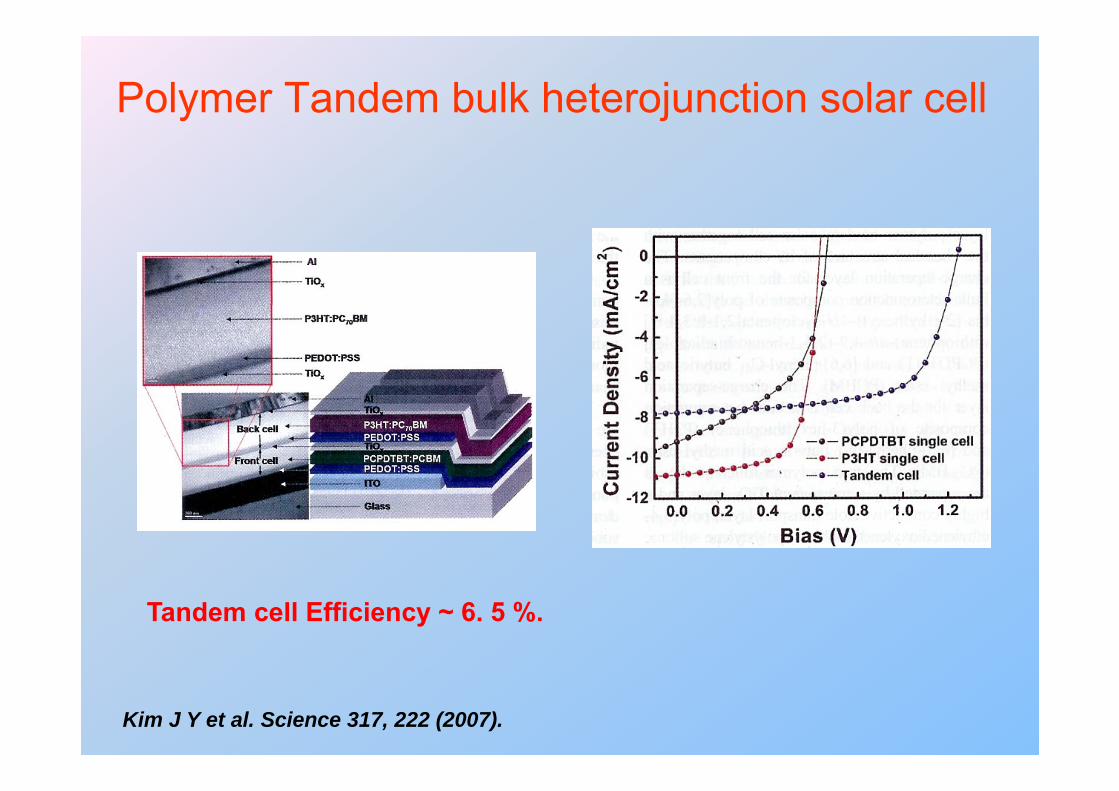
Polymer Tandem bulk heterojunction solar cell
Tandem cell Efficiency ~ 6. 5 %.
Kim J Y et al. Science 317, 222 (2007).
Hybrid Organic-Inorganic Solar CellsPolymer: Inorganic Nanocomposites based Solar cells
Cost EffectiveEfficient Electron Transport Strong Optical AbsorptionEffi i t it di i tiEfficient exciton dissociationPrepared by Inexpensive Wet Chemical Synthesis Possibility of Tailoring the Properties by varying thePossibility of Tailoring the Properties by varying the size of the nanoparticles- quantum size effect
Nanoparticle–polymer cells generally have a photoactive layer consisting of interconnected semiconducting y g gnanoparticles in a solid semiconducting polymer phase i.e. interpenetrating phases of semiconducting polymers and
ti lnanoparticles
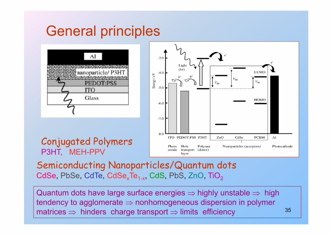
General principles p p
Conjugated PolymersConjugated PolymersP3HT, MEH-PPV
Semiconducting Nanoparticles/Quantum dotsg pCdSe, PbSe, CdTe, CdSexTe1-x, CdS, PbS, ZnO, TiO2
Quantum dots have large surface energies ⇒ highly unstable ⇒ high
35tendency to agglomerate ⇒ nonhomogeneous dispersion in polymer matrices ⇒ hinders charge transport ⇒ limits efficiency
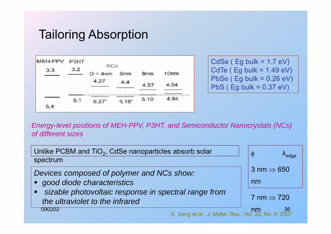
Tailoring Absorption
CdSe ( Eg bulk = 1.7 eV)
Tailoring Absorption
CdSe ( Eg bulk 1.7 eV)CdTe ( Eg bulk = 1.49 eV)PbSe ( Eg bulk = 0.26 eV)PbS ( Eg bulk = 0.37 eV) ( g )
Energy-level positions of MEH-PPV, P3HT, and Semiconductor Nanocrystals (NCs) of different sizes
D i d f l d NC h
Unlike PCBM and TiO2, CdSe nanoparticles absorb solar spectrum
φ λedge
3 nm ⇒ 650Devices composed of polymer and NCs show: good diode characteristics sizable photovoltaic response in spectral range from
3 nm ⇒ 650
nm
7 nm ⇒ 720090202 36the ultraviolet to the infrared
X. Jiang et al., J. Mater. Res., Vol. 22, No. 8, 2007
7 nm ⇒ 720
nm
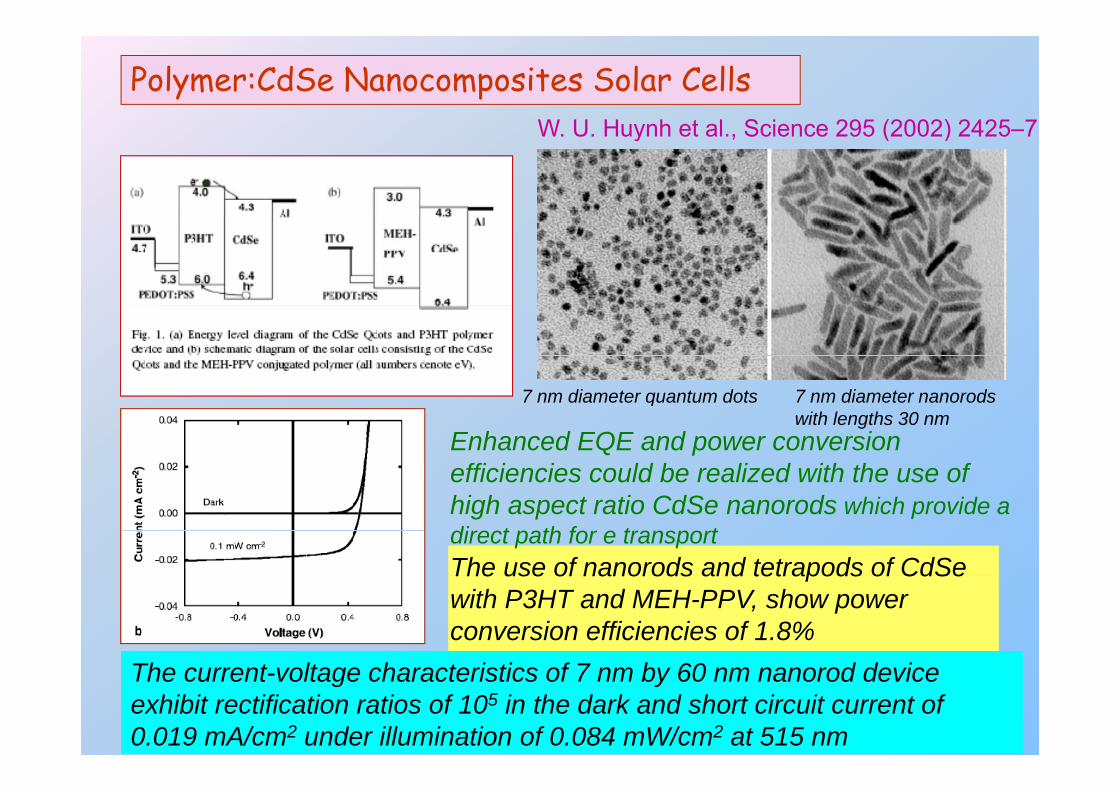
Polymer:CdSe Nanocomposites Solar Cells W U Huynh et al Science 295 (2002) 2425 7W. U. Huynh et al., Science 295 (2002) 2425–7
7 nm diameter nanorods7 nm diameter quantum dots 7 nm diameter nanorods with lengths 30 nm
7 nm diameter quantum dots
Enhanced EQE and power conversion efficiencies could be realized with the use of
The use of nanorods and tetrapods of CdSe
high aspect ratio CdSe nanorods which provide a direct path for e transport
Th t lt h t i ti f 7 b 60 d d i
The use of nanorods and tetrapods of CdSe with P3HT and MEH-PPV, show power conversion efficiencies of 1.8%
090202 37
The current-voltage characteristics of 7 nm by 60 nm nanorod device exhibit rectification ratios of 105 in the dark and short circuit current of 0.019 mA/cm2 under illumination of 0.084 mW/cm2 at 515 nm
Experiment Details for the Synthesis of CdSe Nanoparticles
The organometallic precursor route involves a coordinating solvent TOPO Trioctylphosphine Oxide which is hazardous, unstable, expensive and environmentally unfriendlyMuch cheaper and safer non-TOP-based route for large-p gscale synthesis of CdSe QDs was proposed by Deng et al.(2005)
Procedure:0.0514 g of CdO, 0.1116 g of TDPA and
Chemicals used:CdO - Cadmium OxideTOPO - Trioctylphosphine Oxide 0.0514 g of CdO, 0.1116 g of TDPA and
1.8884 g of TOPO were loaded into a 100 mL flask. The mixture was heated to 300-320 °C d A fl d CdO
TOPO Trioctylphosphine OxideTOP - TrioctylphosphineTDPA - Tetradecylphosphonic AcidSe - Selenium Powder 320 °C under Ar flow, and CdO was
dissolved in TDPA and TOPO. Solution was cooled to 270 °C; selenium stock
Se Selenium PowderCapping agents used:• Trioctylphosphine Oxide (TOPO)• Oleic Acid (OA)
090202 38
solution 1M (0.0205 g of selenium powder dissolved in 1.2 ml of TOP) was injected. After injection nanocrystals grew at 250
( )Cadmium to Selenium ratio:1:1; 2:1; 3:1
Colloidal Particles• Engineer reactions to precipitate quantum dots from
solutions or a host material (e.g. polymer)• In some cases, need to “cap” the surface so the dot
remains chemically stable (i.e. bond other molecules on f )the surface)
• Can form “core-shell” structures• Typically group II-VI materials (e.g. CdS, CdSe)• Size variations ( “size dispersion”)
CdSe core with ZnS shell QDs
Red: bigger dots!Red: bigger dots!
Blue: smaller dots!
Synthesis approach:
12 nm (CdO : Se ~ 0.5:1)
7 nm (CdO : Se ~ 1:1)TOP-Se/Ar gasCdO +
9 nm (CdO : Se ~ 3:1)
5 nm (CdO : Se ~ 2:1)
> 300o C
TOPO/OA- capped CdSe
TOPO/OA + TDPA
Size regulating factor » Cd 5 nm (CdO : Se 2:1)optimized condition
to Se precursor ratio
Preparation of Polymer:CdSe Nanocomposites
Pyridine solvent:- Uncapped CdSe particlesToluene solvent:
C d CdS ti lpp p
- Capped CdSe particles
090202 40
Figure shows the Capped and Uncapped CdSe nanoparticles dispersed in Polymer matrix
Synthesis of CdSe Quantum Dots
Conclusions
We have successfully synthesized high quality CdSe quantum dots
o Nearly-monodispersedo Highly Crystalline
CdS (OA) 2 1
Cd:Se = 2:1 is the optimized condition as for both the capping casessmallest particles were achieved
CdSe(OA) 2:1
CdSe(TOPO) 2:1
~ 7 nm
~ 5 nmCdSe(OA) 2:1 particles show better properties compared to CdSe(TOPO) 2:1
- Steric stability - Photoluminescence
090202 41- Photostability
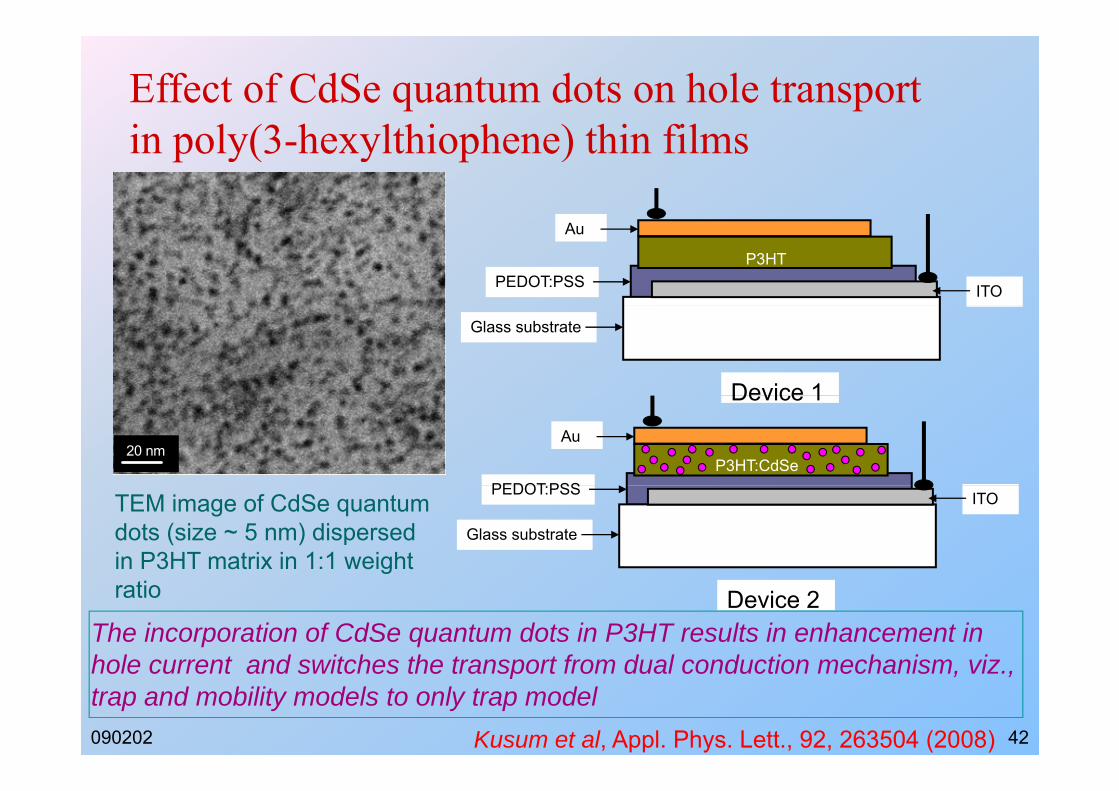
Effect of CdSe quantum dots on hole transport i l (3 h l hi h ) hi filin poly(3-hexylthiophene) thin films
ITOPEDOT:PSSP3HT
Au
Glass substrate
Device 1
20 nm20 nm
Device 1
PEDOT PSSP3HT:CdSe
Au
Glass substrate
ITOPEDOT:PSSTEM image of CdSe quantum dots (size ~ 5 nm) dispersed in P3HT matrix in 1:1 weight
Device 2ratio
The incorporation of CdSe quantum dots in P3HT results in enhancement in hole current and switches the transport from dual conduction mechanism viz
090202 42
hole current and switches the transport from dual conduction mechanism, viz., trap and mobility models to only trap model
Kusum et al, Appl. Phys. Lett., 92, 263504 (2008)
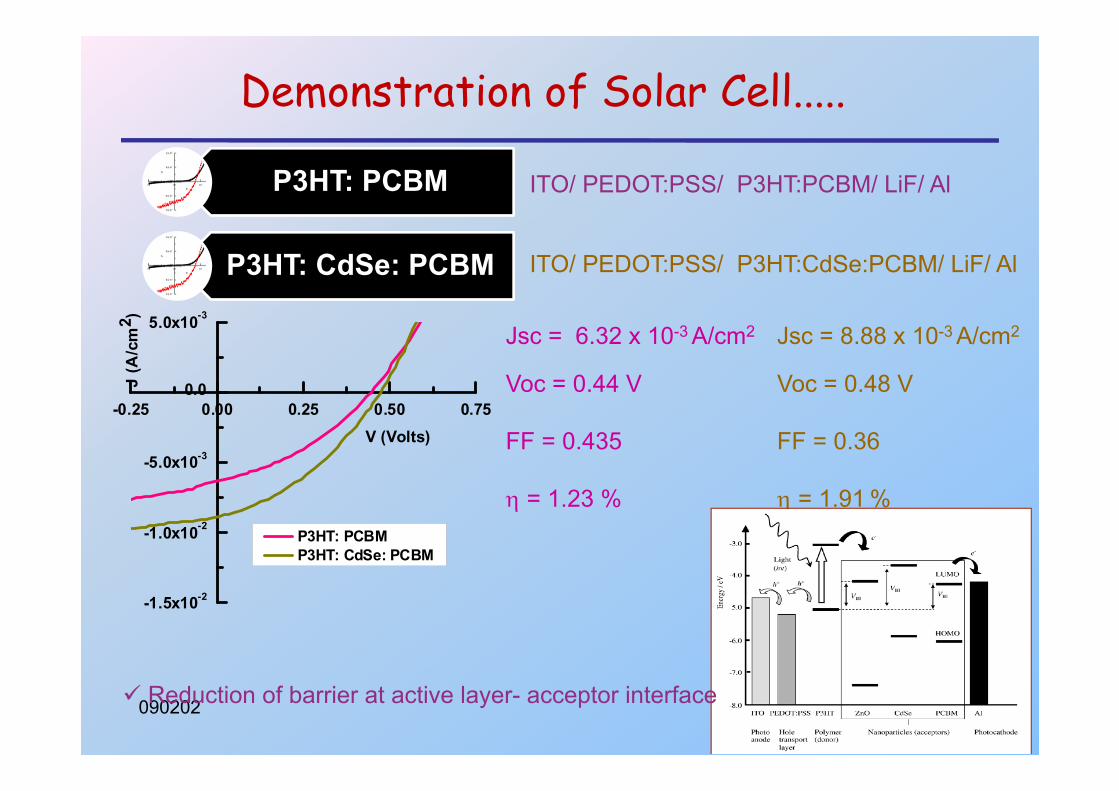
Demonstration of Solar Cell.....
P3HT: PCBM ITO/ PEDOT:PSS/ P3HT:PCBM/ LiF/ Al
P3HT: CdSe: PCBM ITO/ PEDOT:PSS/ P3HT:CdSe:PCBM/ LiF/ Al
Jsc = 6.32 x 10⁻³ A/cm2
Voc = 0.44 V
Jsc = 8.88 x 10⁻³ A/cm2
Voc = 0.48 V0.0
5.0x10⁻³
J (A
/cm
2 )
FF = 0.435 FF = 0.36-0.25 0.00 0.25 0.50 0.75
-5.0x10⁻³V (Volts)
η = 1.23 % η = 1.91 %-1.0x10⁻²
P3HT: PCBM P3HT: CdSe: PCBM
-1.5x10⁻²
090202 43Reduction of barrier at active layer- acceptor interface
Demonstration of Solar Cell.....
MEH-PPV:PCBMMEH
ITO/ PEDOT:PSS/ MEHPPV:PCBM/ LiF/ Al
MEH-PPV:CdSe:PCBM ITO/ PEDOT:PSS/ MEHPPV:CdSe:PCBM/ LiF/ Al
1 00x10-2
Jsc = 2.88 x 10⁻³ A/cm2
Voc = 0.37 V
Jsc = 7.37 x 10⁻³ A/cm2
Voc = 0.41 V5.00x10-3
7.50x10⁻³
1.00x10 MEH-PPV: PCBM MEH-PPV: CdSe: PCBM
A/c
m2 )
FF = 0.46
η = 0 62 %
FF = 0.40
η = 1 47 %-0.25 0.00 0.25 0.50
-2.50x10⁻³
0.00
2.50x10⁻³
J (A
V (Volts) η = 0.62 % η = 1.47 %
-7.50x10⁻³
-5.00x10⁻³
2.50x10
B
V (Volts)A
-1.00x10⁻²
• CdSe QDs have a range of electron affinities reported from 3.5-4.5 eV help in matching energy levels
090202 44
in matching energy levels• PCBM provides additional conducting path allowing significant
enhancement of electron transport at even low doping levels
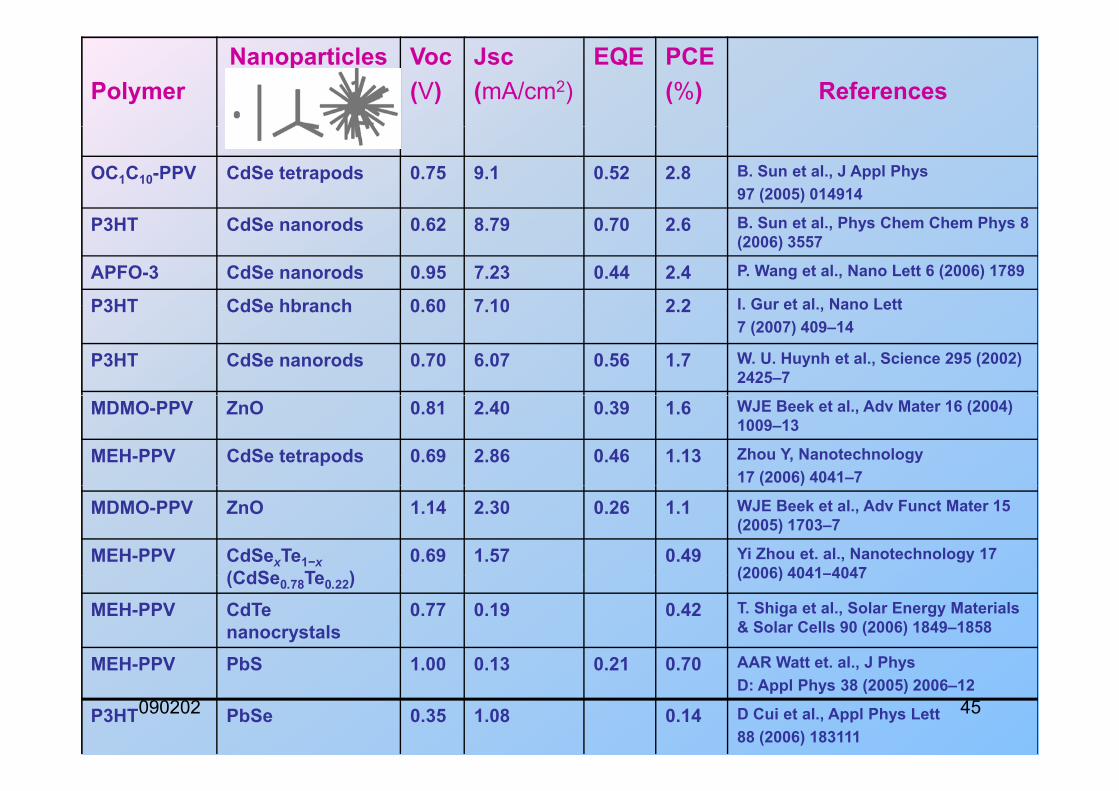
PolymerNanoparticles Voc
(V)Jsc(mA/cm2)
EQE PCE(%) References
OC1C10-PPV CdSe tetrapods 0.75 9.1 0.52 2.8 B. Sun et al., J Appl Phys97 (2005) 014914
P3HT CdSe nanorods 0.62 8.79 0.70 2.6 B. Sun et al., Phys Chem Chem Phys 8 (2006) 3557
APFO-3 CdSe nanorods 0.95 7.23 0.44 2.4 P. Wang et al., Nano Lett 6 (2006) 1789
P3HT CdSe hbranch 0 60 7 10 2 2 I Gur et al Nano LettP3HT CdSe hbranch 0.60 7.10 2.2 I. Gur et al., Nano Lett7 (2007) 409–14
P3HT CdSe nanorods 0.70 6.07 0.56 1.7 W. U. Huynh et al., Science 295 (2002) 2425–7
MDMO-PPV ZnO 0.81 2.40 0.39 1.6 WJE Beek et al., Adv Mater 16 (2004) 1009–13
MEH-PPV CdSe tetrapods 0.69 2.86 0.46 1.13 Zhou Y, Nanotechnology17 (2006) 4041–7( )
MDMO-PPV ZnO 1.14 2.30 0.26 1.1 WJE Beek et al., Adv Funct Mater 15 (2005) 1703–7
MEH-PPV CdSexTe1−x(CdSe Te )
0.69 1.57 0.49 Yi Zhou et. al., Nanotechnology 17 (2006) 4041–4047(CdSe0.78Te0.22) (2006) 4041 4047
MEH-PPV CdTe nanocrystals
0.77 0.19 0.42 T. Shiga et al., Solar Energy Materials & Solar Cells 90 (2006) 1849–1858
MEH-PPV PbS 1 00 0 13 0 21 0 70 AAR Watt et al J Phys
090202 45
MEH-PPV PbS 1.00 0.13 0.21 0.70 AAR Watt et. al., J PhysD: Appl Phys 38 (2005) 2006–12
P3HT PbSe 0.35 1.08 0.14 D Cui et al., Appl Phys Lett88 (2006) 183111
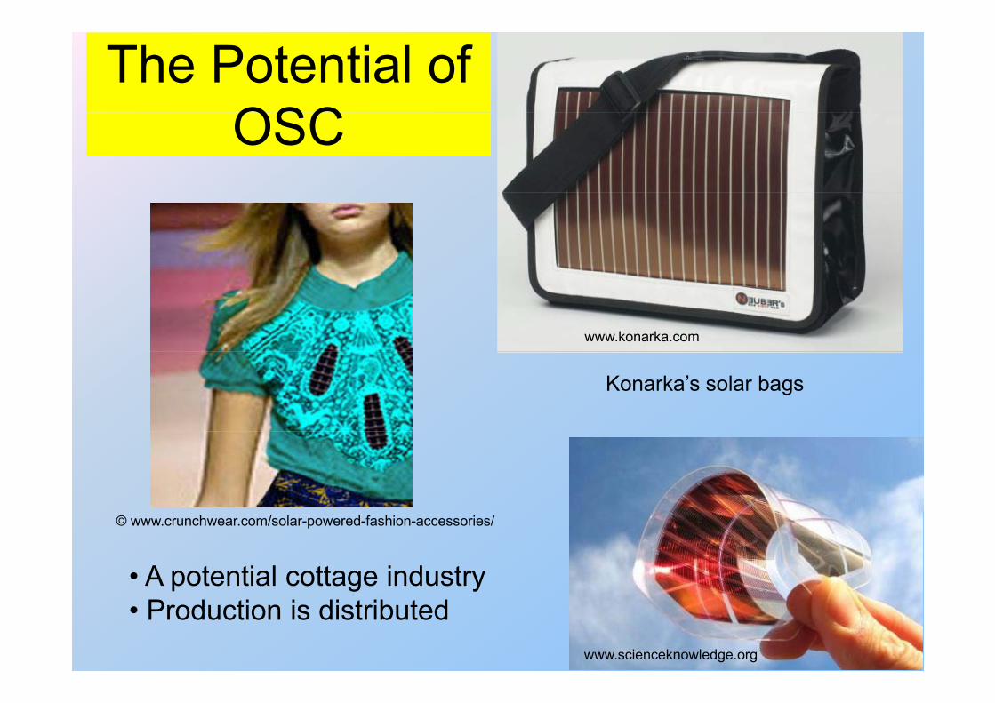
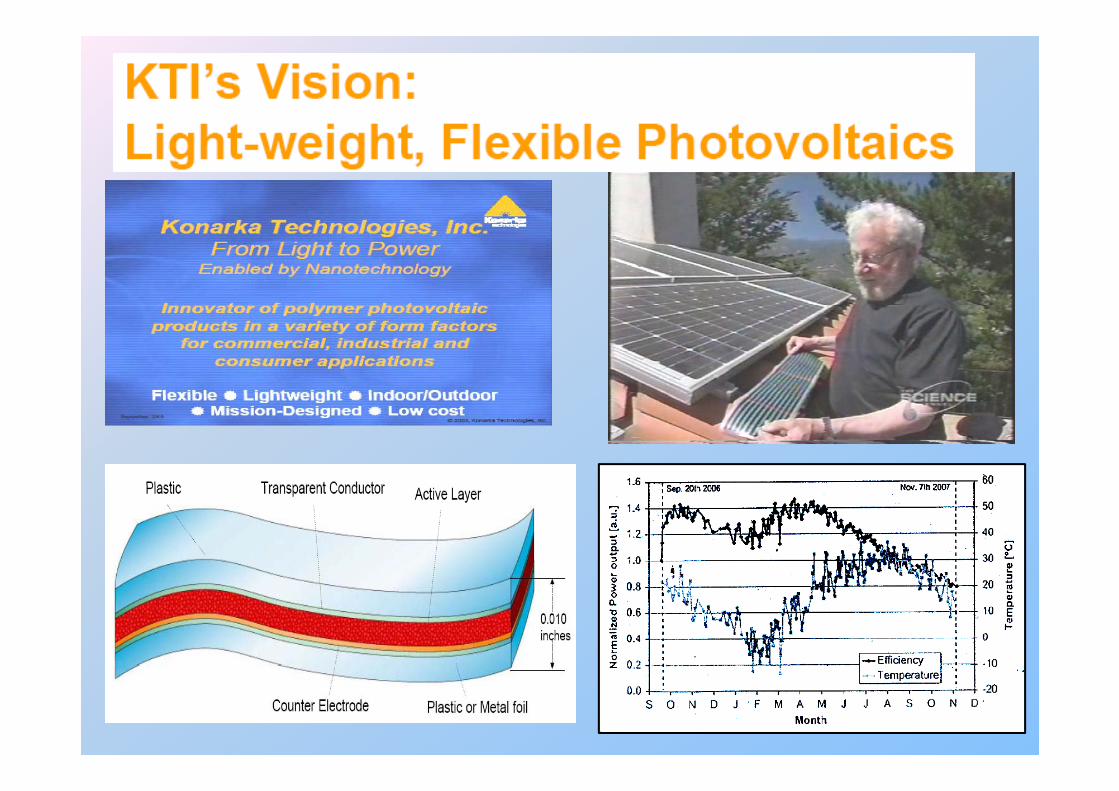
The Potential of OSCOSC
www.konarka.com
Konarka’s solar bags
• A potential cottage industry
© www.crunchwear.com/solar-powered-fashion-accessories/
p g y• Production is distributed
www.scienceknowledge.org
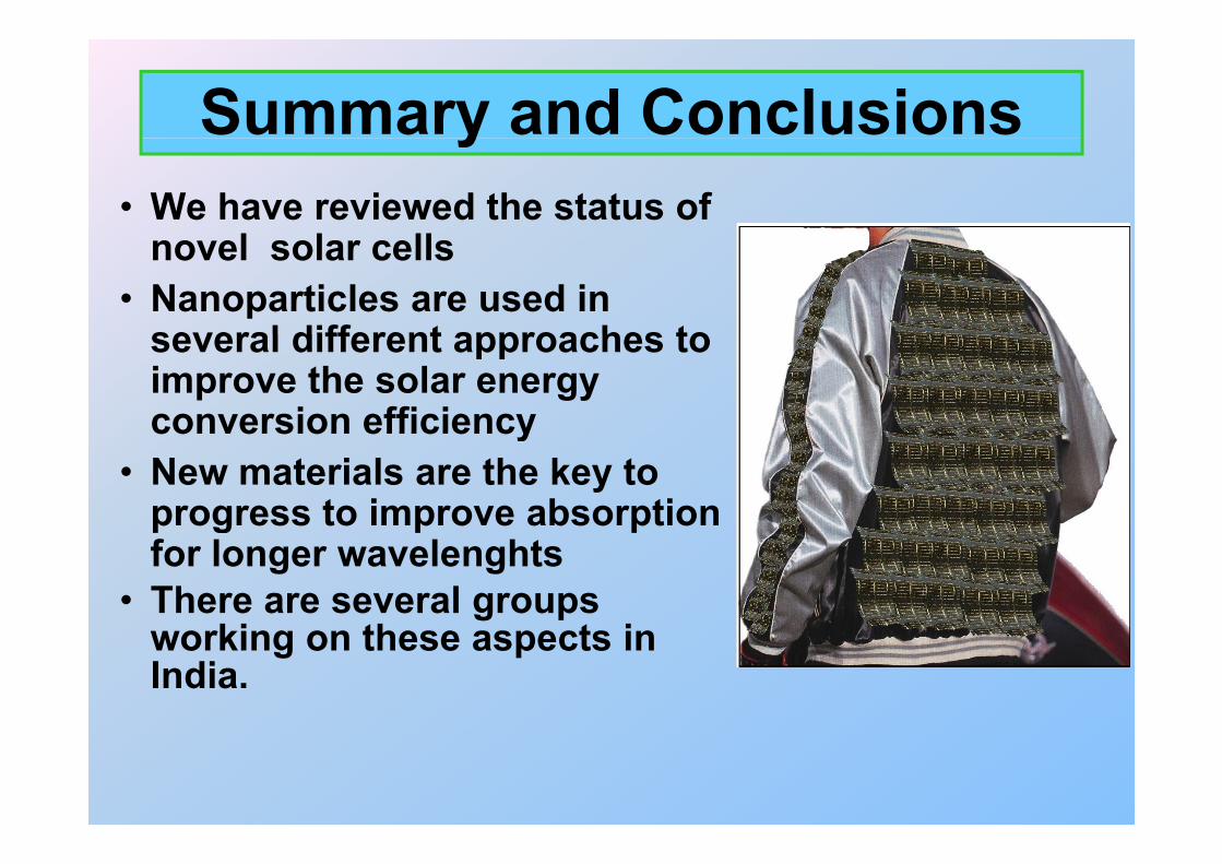
Summary and Conclusions• We have reviewed the status of
l l ll
y
novel solar cells• Nanoparticles are used in
several different approaches toseveral different approaches to improve the solar energy conversion efficiencyconversion efficiency
• New materials are the key to progress to improve absorption p g p pfor longer wavelenghts
• There are several groups ki th t iworking on these aspects in
India.

I thank numerous persons who have contributed to this presentation p
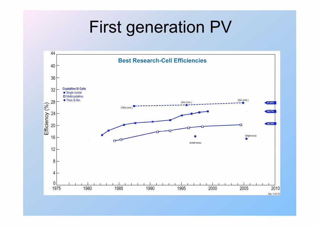
First generation PVg
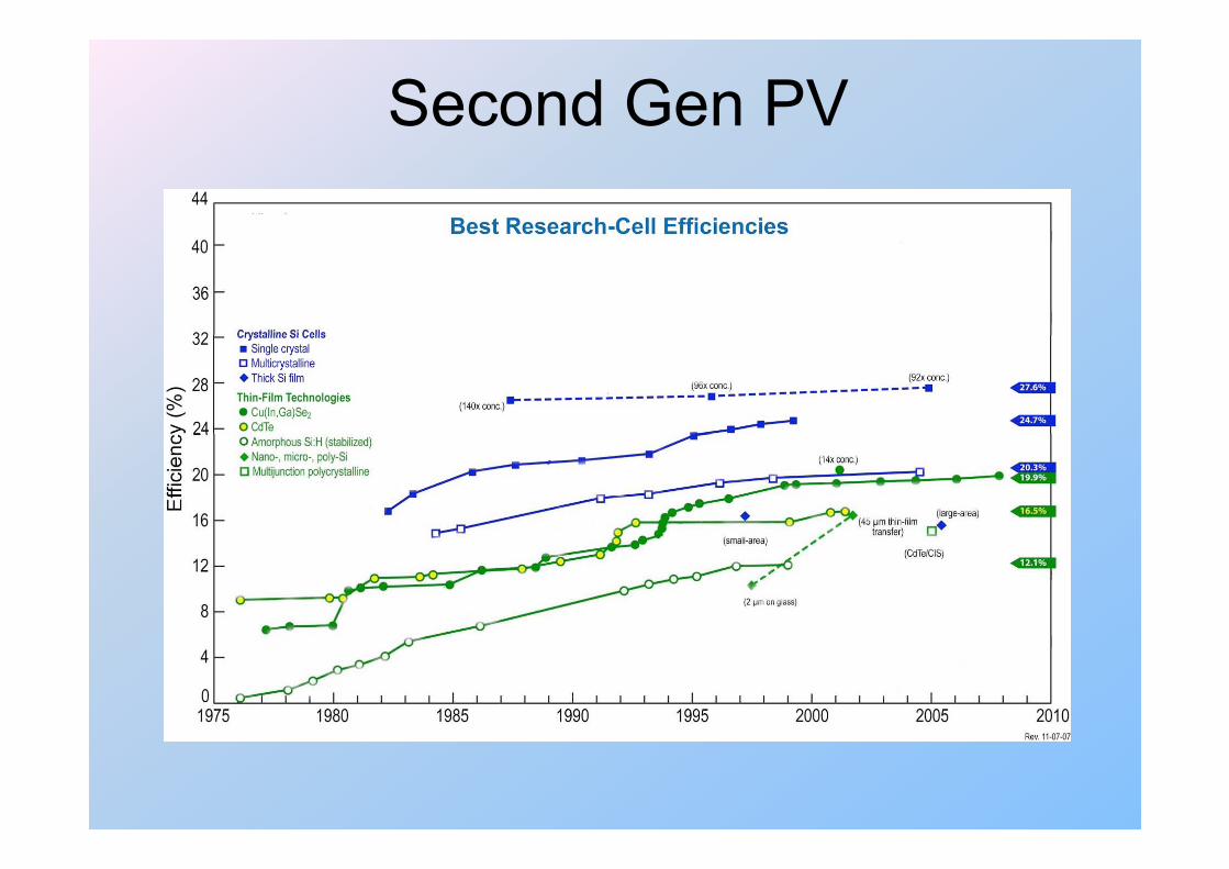
Second Gen PV
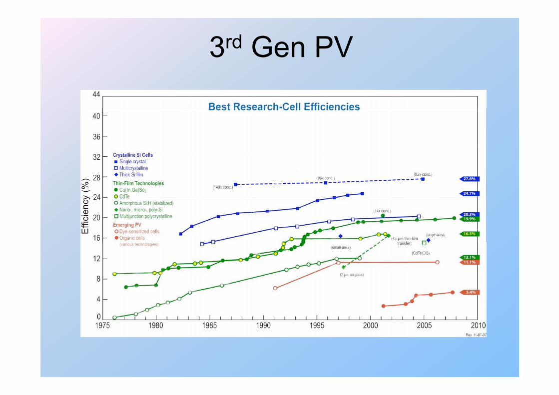
3rd Gen PV
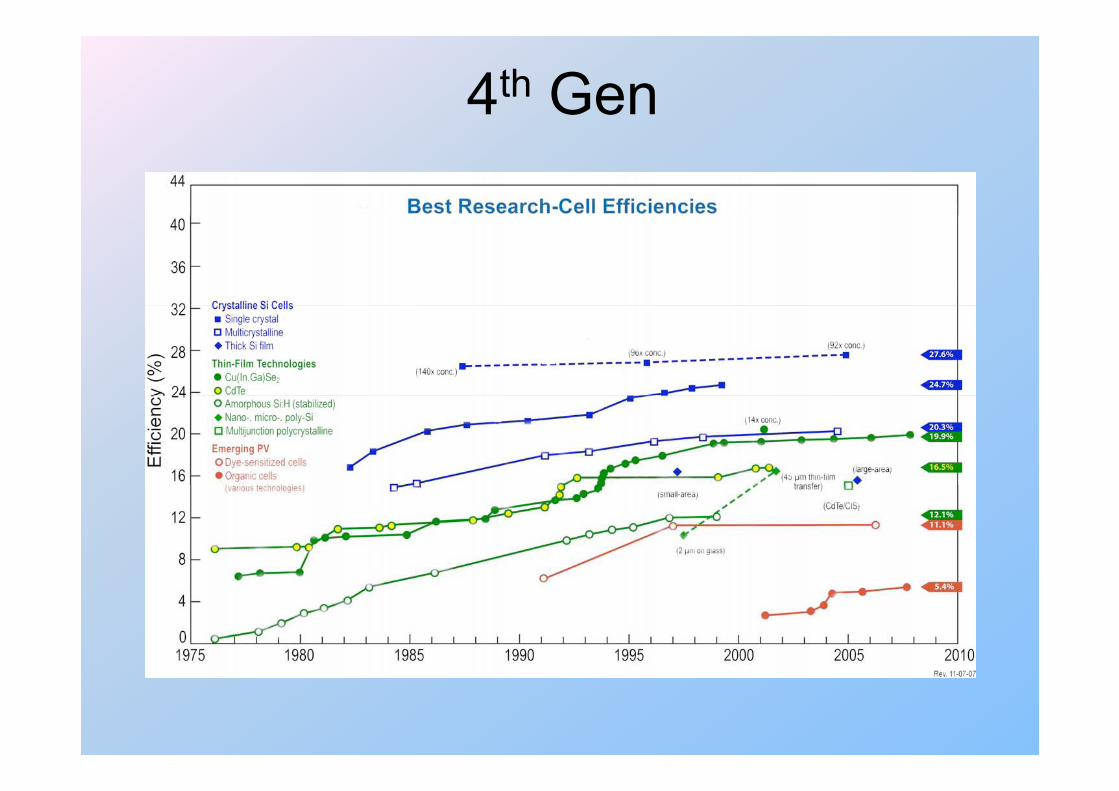
4th Gen

Absorption BandAbsorption Band
m-1
)
m-1
)
cien
t (cm GaAs
(Inorganic)
cien
t (cm CuPC
(organic)
n C
oeffi
c
n C
oeffi
c
Narrow Band
sorp
tion
bsor
ptio
n
Narrow Band
Abs
Energy (eV)Energy (eV)
Energy (eV)
Ab
Organic absorbs in a narrow bands Inorganics absorb in wider bandsOrganic absorbs in a narrow bands Inorganics absorb in wider bands
+ Can use multiple layers(tandem solar cells)
Absorbs all photons in solar spectrumwith energy above bandgap energy( )
The absorption coefficient values are usually higher in organic solar

Exciton FormationExciton Formationhν
LUMO level
El t it d
HOMO level
Electron excitedto higher energy level
• Absorbed photon creates an exciton• Excitons do NOT always form free electrons and
holes o es– This is especially true in organic semiconductors– Here, strong field are needed to dissociate excitonsHere, strong field are needed to dissociate excitons
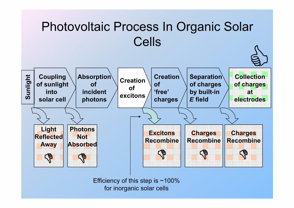
Photovoltaic Process In Organic Solar gCells
Coupling Absorption Creation Separation CollectionCreationht
of sunlightinto
solar cell
of incidentphotons
of ‘free’ charges
of chargesby built-inE field
of chargesat
electrodes
Creationof
excitonsSunl
ig
Li ht Ph tLightReflected
Away
PhotonsNot
Absorbed
ChargesRecombine
ChargesRecombine
ExcitonsRecombine
Efficiency of this step is ~100%for inorganic solar cells
Built in FieldBuilt-in Field
φbiEf φbi
Eb ilt i n-typep-type Ebuilt-in
Ebuilt-in
O i M t i lOrganicMaterial Inorganic semiconductord
No charge of its ownBuilt-in potential depends on electrode work function difference
In Typical OSCIn Typical OSCOSC is typically different from inorganic solar cells in the following ways:
• Absorption in a narrower spectral bandAbsorption in a narrower spectral band
• Usually high absorption coefficienty g p
• Exciton binding energy higherg gy g
• Poor charge mobilityg y
• Built-in potential dependent on electrodes

At IIT Kanpur
Product Oriented ResearchProduct Oriented Research
220 m2 ISO 6 Cleanroom220 m2 ISO 6 Cleanroom
http://www.iitk.ac.in/scdt/
Members of SCDTFaculty Scientists/ Research
Members of SCDTFaculty
• Dr. Deepak Gupta• Dr. Y.N.Mohapatra• Dr. Dr. B.Mazhari
Dr Monica Katiyar
Scientists/ Research Engineers
• Dr. J. Narain• Dr. Monica Katiyar• Dr. Satyendra Kumar• Dr. S.S.K.Iyer• Dr. Ashish Garg• Dr Sidhartha Panda
• Dr. Vandana Singh• Dr. Ashish Gupta
• Dr. Sidhartha Panda
Visiting Research Engineers
• Dr. Unni Narain• Dr. Asha Awasthi• Mr. I. V. Kameshwar Rao
Mr Ranbir Singh
Support Staff
Mr. Dharmendra SwainMr. Arvind Kumar Students
• Mr. Ranbir Singh• Mr. Boby C. Villari• Mr. Pankaj Uttwani• Dr. Ganesan Palaniswami
Mr. Ramnath YadavMr. Dinesh KumarMr. Ajay NaikMs. Mamata Rai
Ph.D : 19M.Tech : 22B Tech/ M Sc : 15
Ms. Shewta MauryaB.Tech/ M.Sc.: 15
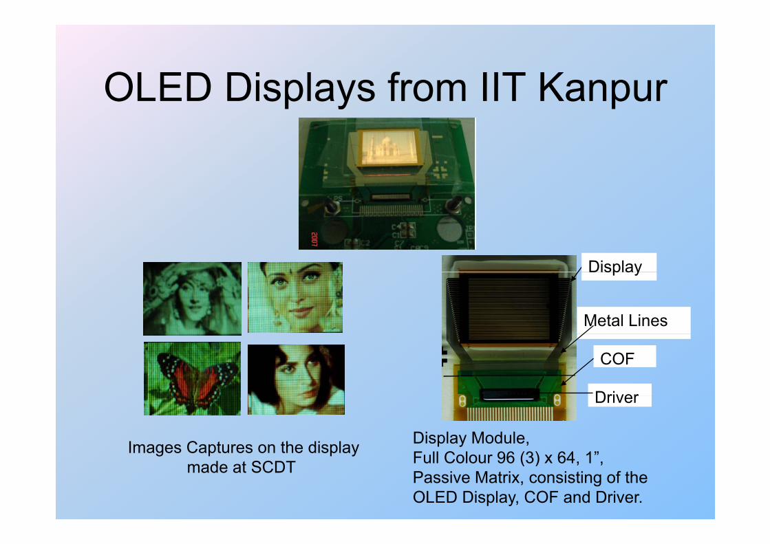
OLED Displays from IIT KanpurOLED Displays from IIT Kanpur
DisplayDisplay
Metal Lines
COF
Driver
Images Captures on the display
Driver
Display Module, Full Colour 96 (3) x 64 1”made at SCDT Full Colour 96 (3) x 64, 1 , Passive Matrix, consisting of the OLED Display, COF and Driver.
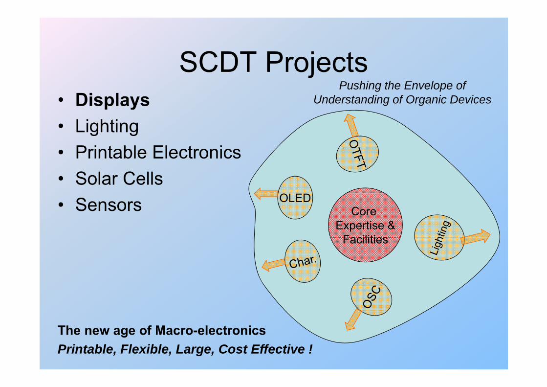
SCDT ProjectsPushing the Envelope of
Understanding of Organic Devices
SCDT Projects• Displays g gDisplays• Lighting
Printable Electronics
O
• Printable Electronics• Solar Cells
Core Expertise &
Facilities
OLED• Sensors
Facilities
fThe new age of Macro-electronicsPrintable, Flexible, Large, Cost Effective !
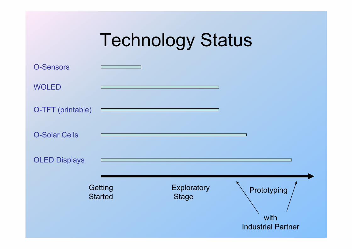
Technology StatusTechnology StatusO-Sensors
WOLED
O Sensors
O-TFT (printable)
O-Solar Cells
OLED Displays
GettingStarted
ExploratoryStage
Prototyping
withIndustrial Partner

On-going work at IIT Kanpur
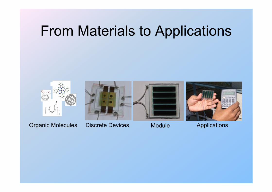
From Materials to ApplicationsFrom Materials to Applications
Discrete Devices Module ApplicationsOrganic Molecules
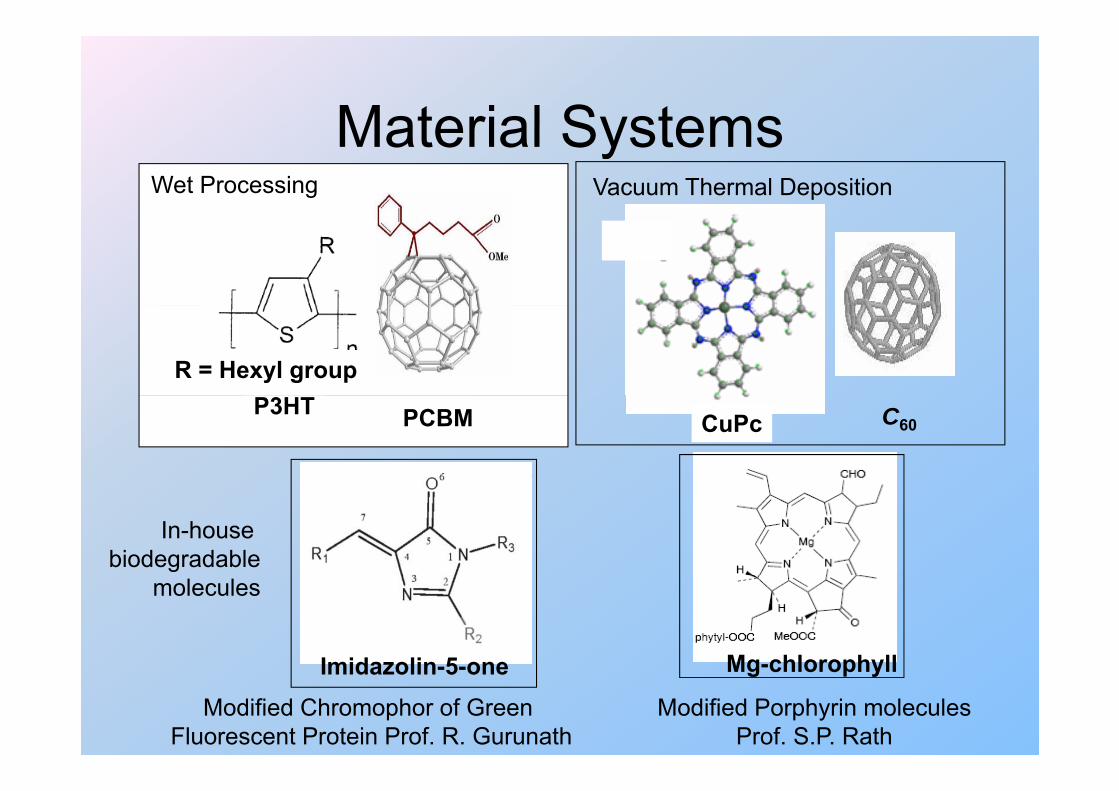
Material SystemsMaterial SystemsVacuum Thermal DepositionWet Processing
R = Hexyl group
C60CuPcPCBMP3HT
In-house biodegradable
Mg-chlorophyllImidazolin 5 one
molecules
Mg-chlorophyllImidazolin-5-oneModified Chromophor of Green
Fluorescent Protein Prof. R. GurunathModified Porphyrin molecules
Prof. S.P. Rath
Four Pronged ApproachFour Pronged Approach• Characterising the devices• Characterising the devices
– Spectral response characterisation– Spectral ellipsometry
• Increasing efficiency of device• Increasing efficiency of device– Physics and circuit model of organic solar cells– Choice of material
St t bl d bil t d– Structure – blend, bilayer, tandem …– Process optimisation
• Reliability and stability– Choice of material– Mechanism of degradation– Encapsulation techniquesp q
• New & emerging technology issues– Novel methods of fabrication– System level issuesSystem level issues
Spectral Response AnalysisSuman Banerjee
Spectral Response Analysis
Suman Banerjee

P3HT:PCBM Solar CellP3HT:PCBM Solar Cell
Calcium-Aluminium CathodeCalcium Aluminium CathodeP3HT:PCBM Blend
PEDOT:PSS ITO
PEDOT:PSS - 30 nm;
ITO Glass
P3HT:PCBM (1:1) - 90 nm; Ca - 6 nm; Al - 70 nm.
Characterstics of a typical Organic (Polymer) Solar CellArun Tej Mallajosyula

Effect of Post Process AnnealAnirban Bagui
Effect of Post Process AnnealP3HT: PCBM Blend
H t t t
Aluminium CathodePolymer BlendHeterostructure Polymer Blend PEDOT:PSS ITO Glass
Vinod Pagare 2007

Solvent Drying in E FieldSolvent Drying in E-Field
Electric Field Annealing during solvent drying step of active layerElectric Field Annealing during solvent drying step of active layer improves device efficiency
Anirban Bagui Indian Patent being filed
Modifying Interface by Annealing
As deposited CuPc Annealed CuPcSmoother
Specially Annealed CuPcSmoother with pillars
C60Al
Modification of interfaceActive
ITOCuPc
Modification of interfacebetween CuPc and C60
ActiveArea
Glass
Anukul Prasad Parhi Indian Patent being filed

Nanotubes in Polymer OSCNanotubes in Polymer OSC
0 60.91.2
P3HT:PCBM:SWNT (0.75 %) P3HT:PCBM
24
FF
565
570 Voc5.0 Jsc
0.0 0.1 0.2 0.3 0.4 0.50.00.30.6
mA
cm
-2) Voltage (V)
18
21
560
565
4.0
4.5Jsc Voc
FF(%)
(mV)(mA cm-2)
0 9-0.6-0.3
η = 2.99 %η = 2.01 %
J L (m
AM 1.5 G 15
18
5553.5
-1.2-0.9
Intensity = 6 mW cm-20.0 0.2 0.4 0.6 0.8 1.0
15
SWNT wt%
5503.0
•Incorporation of single walled nanotubes can improve solar cell performance•Main role of nanotube is in charge transport within the solar cellNanotube does not have much effect in exciton generation or dissociation•Nanotube does not have much effect in exciton generation or dissociation
Aurn Tej Mallajosyula
Degradation ModelsDegradation ModelsDegradation under Electrical & Optical Stress
• Statistically arrive at parameters that matter most• Identify the physics of degradation• Use learning to increase device lifetime
Munish Jassi 2006
• Use learning to increase device lifetime
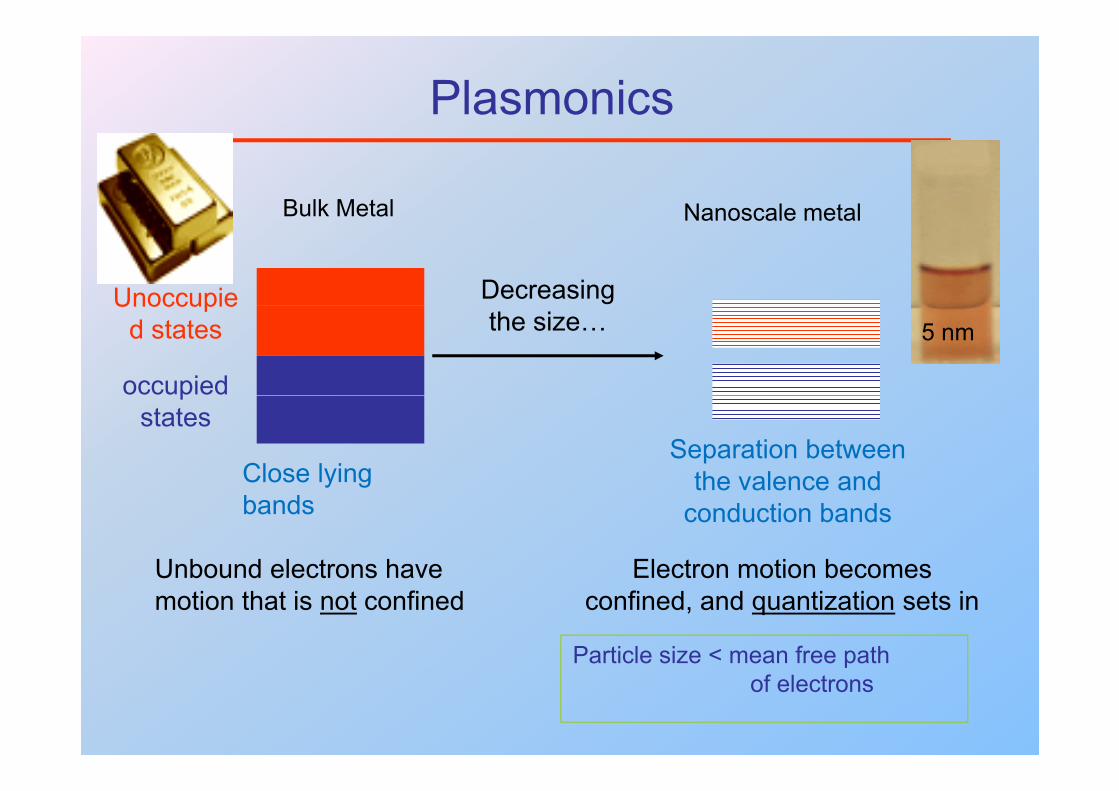
Plasmonics
Bulk Metal Nanoscale metal
Decreasing
Bulk Metal
Unoccupie
Nanoscale metal
the size…Unoccupie
d states
occupied
5 nm
Close lying
pstates
Separation between the valence and
Unbound electrons have
y gbands
Electron motion becomes
the valence and conduction bands
Unbound electrons have motion that is not confined
Electron motion becomes confined, and quantization sets in
Particle size < mean free path pof electrons
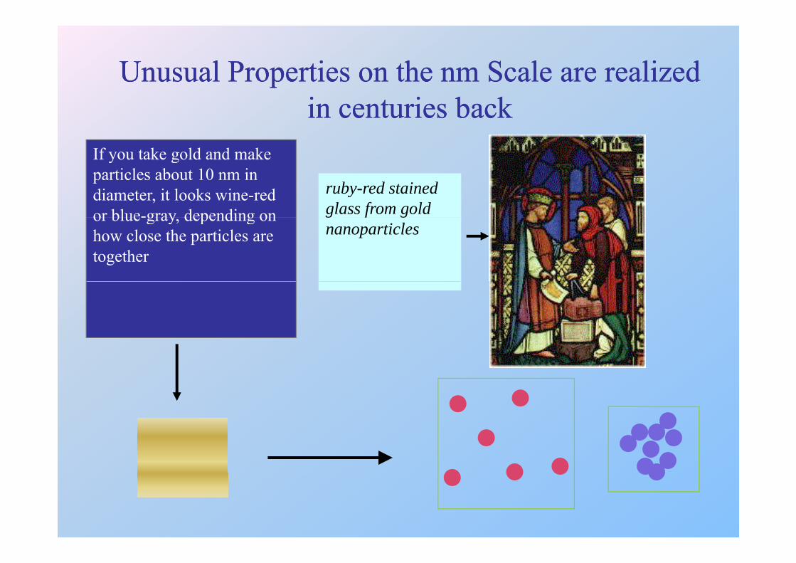
Unusual Properties on the nm Scale Unusual Properties on the nm Scale are realizedare realizedin centuries backin centuries back
If you take gold and makeIf you take gold and make particles about 10 nm in diameter, it looks wine-red or blue-gray depending on
ruby-red stained glass from goldor blue gray, depending on
how close the particles are together
nanoparticles
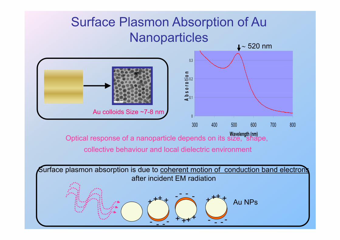
Surface Plasmon Absorption of Au NanoparticlesNanoparticles
0.3
∼ 520 nm
0.2
sorp
tion
0
0.1Abs
Au colloids Size ~7-8 nm
300 400 500 600 700 800Wavelength (nm)Optical response of a nanoparticle depends on its size, shape,
ll ti b h i d l l di l t i i t
Surface plasmon absorption is due to coherent motion of conduction band electrons
collective behaviour and local dielectric environment
after incident EM radiation
+ +++ + +++Au NPs
-
+ +
- - - -- - -
Au NPs
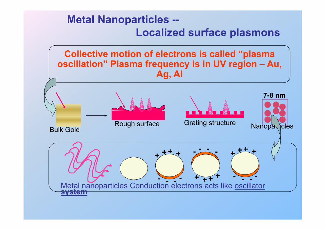
Metal Nanoparticles --Localized surface plasmonsp
Collective motion of electrons is called “plasma oscillation” Plasma frequency is in UV region Auoscillation” Plasma frequency is in UV region – Au,
Ag, Al
7-8 nm
Rough surface Grating structure NanoparticlesBulk Gold
+ ++ + + ++ +
-- - - -- - -Metal nanoparticles Conduction electrons acts like oscillator systemsystem
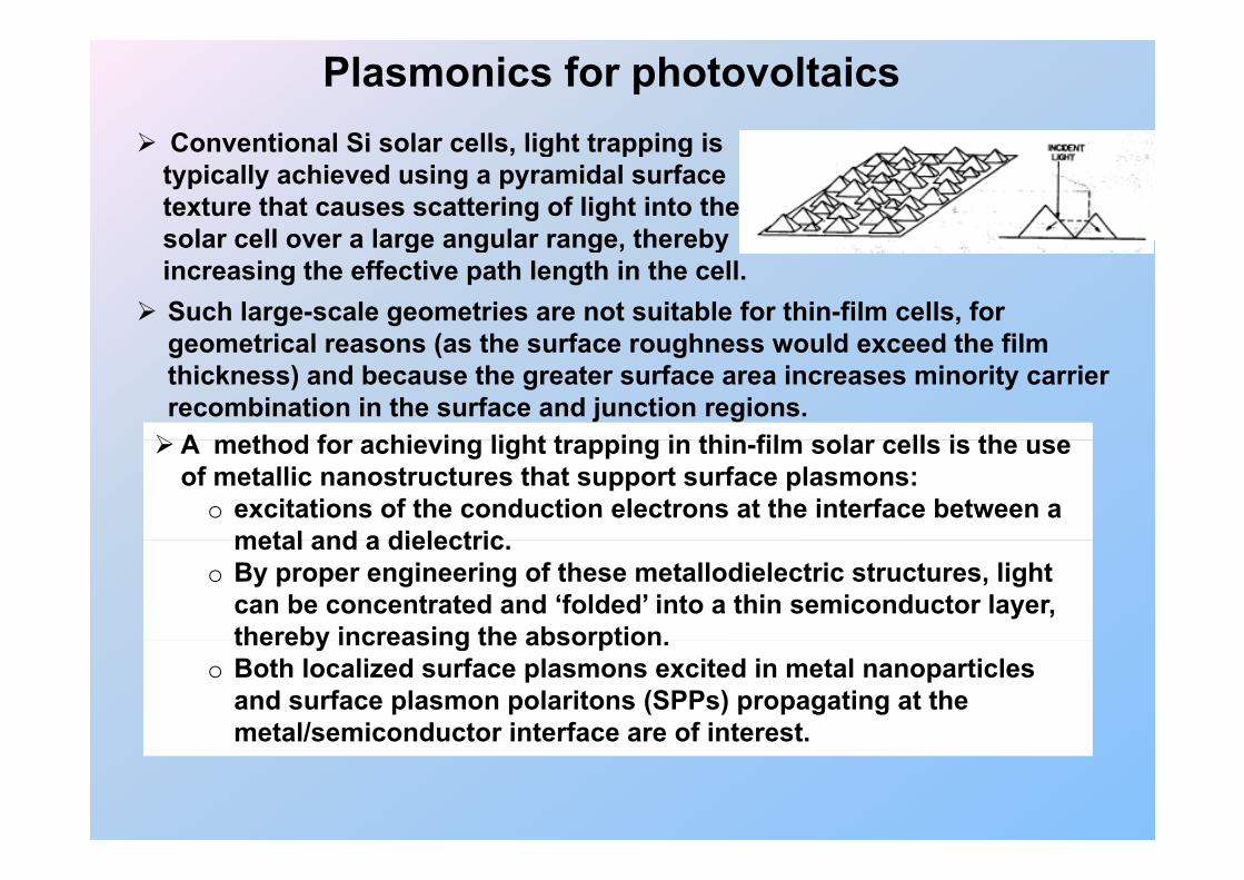
Plasmonics for photovoltaicsConventional Si solar cells light trapping isConventional Si solar cells, light trapping is typically achieved using a pyramidal surface texture that causes scattering of light into the solar cell over a large angular range therebysolar cell over a large angular range, thereby increasing the effective path length in the cell.Such large-scale geometries are not suitable for thin-film cells, for geometrical reasons (as the surface roughness would exceed the film
A method for achieving light trapping in thin film solar cells is the use
geometrical reasons (as the surface roughness would exceed the film thickness) and because the greater surface area increases minority carrier recombination in the surface and junction regions.A method for achieving light trapping in thin-film solar cells is the use of metallic nanostructures that support surface plasmons:
o excitations of the conduction electrons at the interface between a metal and a dielectricmetal and a dielectric.
o By proper engineering of these metallodielectric structures, light can be concentrated and ‘folded’ into a thin semiconductor layer, thereby increasing the absorptionthereby increasing the absorption.
o Both localized surface plasmons excited in metal nanoparticlesand surface plasmon polaritons (SPPs) propagating at the metal/semiconductor interface are of interest.metal/semiconductor interface are of interest.
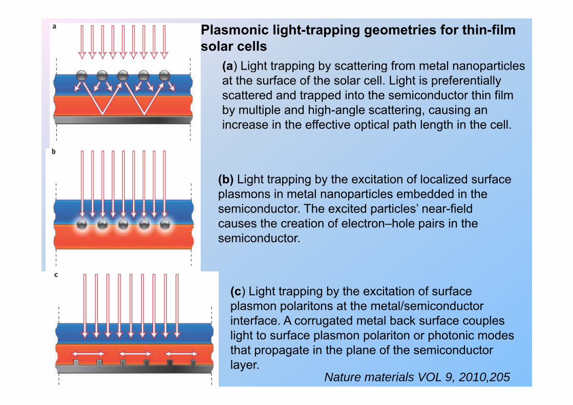
Plasmonic light-trapping geometries for thin-film solar cells
(a) Light trapping by scattering from metal nanoparticles(a) Light trapping by scattering from metal nanoparticles at the surface of the solar cell. Light is preferentially scattered and trapped into the semiconductor thin film by multiple and high-angle scattering causing anby multiple and high-angle scattering, causing an increase in the effective optical path length in the cell.
(b) Light trapping by the excitation of localized surface plasmons in metal nanoparticles embedded in the semiconductor. The excited particles’ near-field causes the creation of electron–hole pairs in the semiconductor.
(c) Light trapping by the excitation of surface(c) Light trapping by the excitation of surface plasmon polaritons at the metal/semiconductor interface. A corrugated metal back surface couples light to surface plasmon polariton or photonic modes g p p pthat propagate in the plane of the semiconductor layer.
Nature materials VOL 9, 2010,205
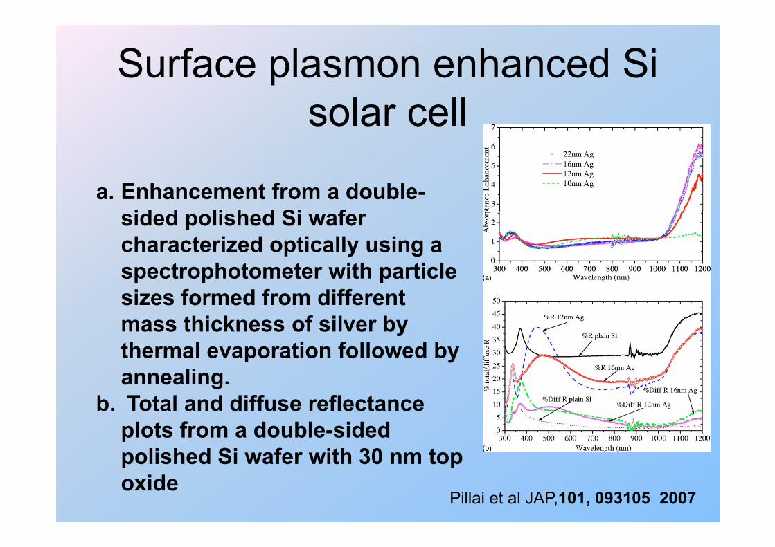
Surface plasmon enhanced Si solar cell
a. Enhancement from a double-id d li h d Si fsided polished Si wafer
characterized optically using a spectrophotometer with particlespectrophotometer with particle sizes formed from different mass thickness of silver by ythermal evaporation followed by annealing.
b T t l d diff fl tb. Total and diffuse reflectance plots from a double-sided polished Si wafer with 30 nm toppolished Si wafer with 30 nm top oxide
Pillai et al JAP,101, 093105 2007
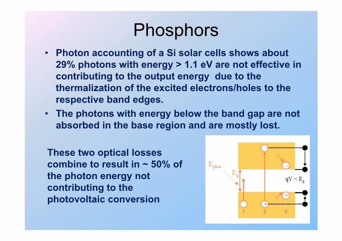
Phosphors• Photon accounting of a Si solar cells shows about
29% photons with energy > 1 1 eV are not effective in
p
29% photons with energy > 1.1 eV are not effective in contributing to the output energy due to the thermalization of the excited electrons/holes to the respective band edges.
• The photons with energy below the band gap are not absorbed in the base region and are mostly lost.
These two optical losses combine to result in ~ 50% of the photon energy notthe photon energy not contributing to the photovoltaic conversion p
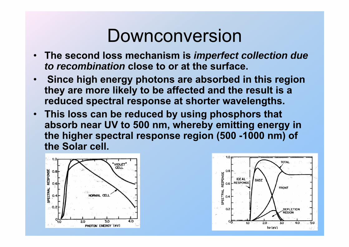
DownconversionDownconversion• The second loss mechanism is imperfect collection due
to recombination close to or at the surfaceto recombination close to or at the surface.• Since high energy photons are absorbed in this region
they are more likely to be affected and the result is a y yreduced spectral response at shorter wavelengths.
• This loss can be reduced by using phosphors that absorb near UV to 500 nm whereby emitting energy inabsorb near UV to 500 nm, whereby emitting energy in the higher spectral response region (500 -1000 nm) of the Solar cell.
UpconversionUpconversionTh thi d l h i i t i i hi h• The third loss mechanism is transmission, which occurs because photons with energy less than the band gap of silicon are not absorbed.g p
• Transmission losses can be reduced by employing up-conversion (UC) processes, whereby two or more l h t bi t t hi hlow energy photons combine to create one higher energy photon.
• Spectrum modification is the most promising• Spectrum modification is the most promising solution for enhancing the cell efficiency but unfortunately, no breakthrough has been reported
t i thi Thi k th i t tyet in this area. This makes the issue more target-oriented and challenging to pursue research for suitable phosphor/nanophosphor coatings forsuitable phosphor/nanophosphor coatings for improvements in the efficiency of solar cell.
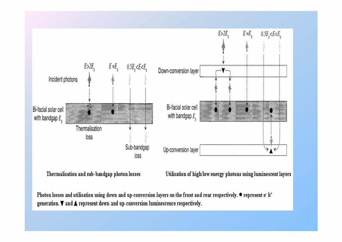
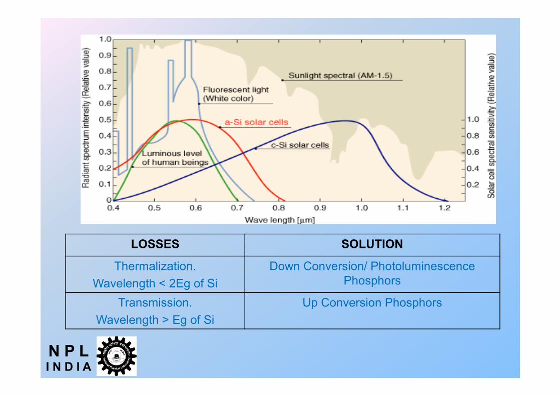
LOSSES SOLUTIONLOSSES SOLUTION
Thermalization.Wavelength < 2Eg of Si
Down Conversion/ Photoluminescence Phosphorsg g
Transmission.Wavelength > Eg of Si
Up Conversion Phosphors
N P LI N D I A
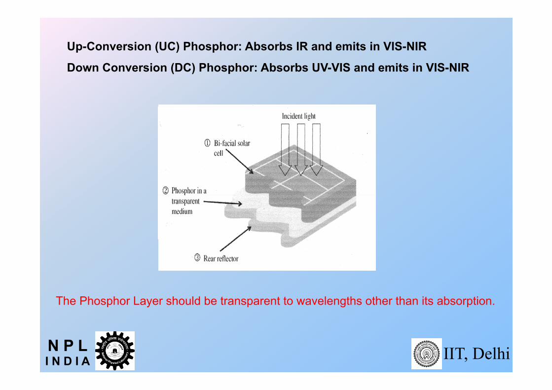
Up-Conversion (UC) Phosphor: Absorbs IR and emits in VIS-NIR
Down Conversion (DC) Phosphor: Absorbs UV-VIS and emits in VIS-NIR
The Phosphor Layer should be transparent to wavelengths other than its absorption.
N P LI N D I A IIT, Delhi
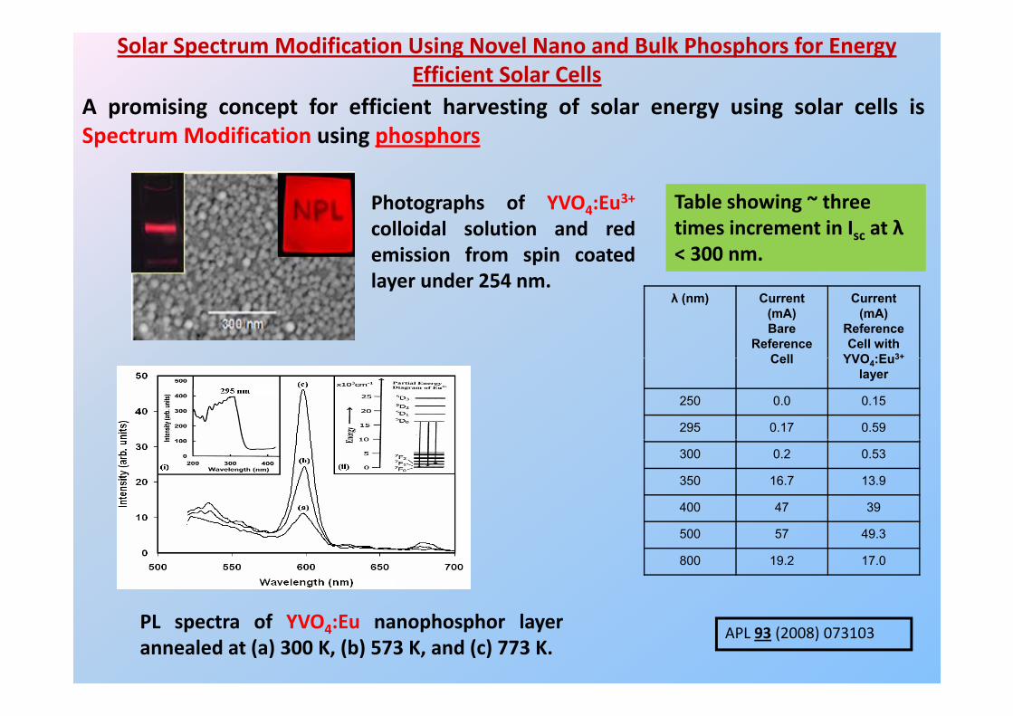
Solar Spectrum Modification Using Novel Nano and Bulk Phosphors for Energy Efficient Solar Cells
A promising concept for efficient harvesting of solar energy using solar cells is
h h f O 3+ T bl h i h
p o s g co cept o e c e t a est g o so a e e gy us g so a ce s sSpectrum Modification using phosphors
Photographs of YVO4:Eu3+
colloidal solution and redemission from spin coatedl d 254
Table showing ~ three times increment in Isc at λ< 300 nm.
λ (nm) Current (mA)Bare
Reference Cell
Current (mA)
Reference Cell with
YVO :Eu3+
layer under 254 nm.
Cell YVO4:Eu3+
layer
250 0.0 0.15
295 0.17 0.59
300 0.2 0.53
350 16.7 13.9
400 47 39
500 57 49.3
800 19.2 17.0
PL spectra of YVO4:Eu nanophosphor layerannealed at (a) 300 K, (b) 573 K, and (c) 773 K.
APL 93 (2008) 073103
Thin-film structures can reduce the costThin-film structures can reduce the cost of solar power by using inexpensive
b t t d l tit dsubstrates and a lower quantity and quality of semiconductor material. However, the resulting short optical path length and minority carrier diffusion g ylength necessitates either a high absorption coefficient or excellent lightabsorption coefficient or excellent light trapping.
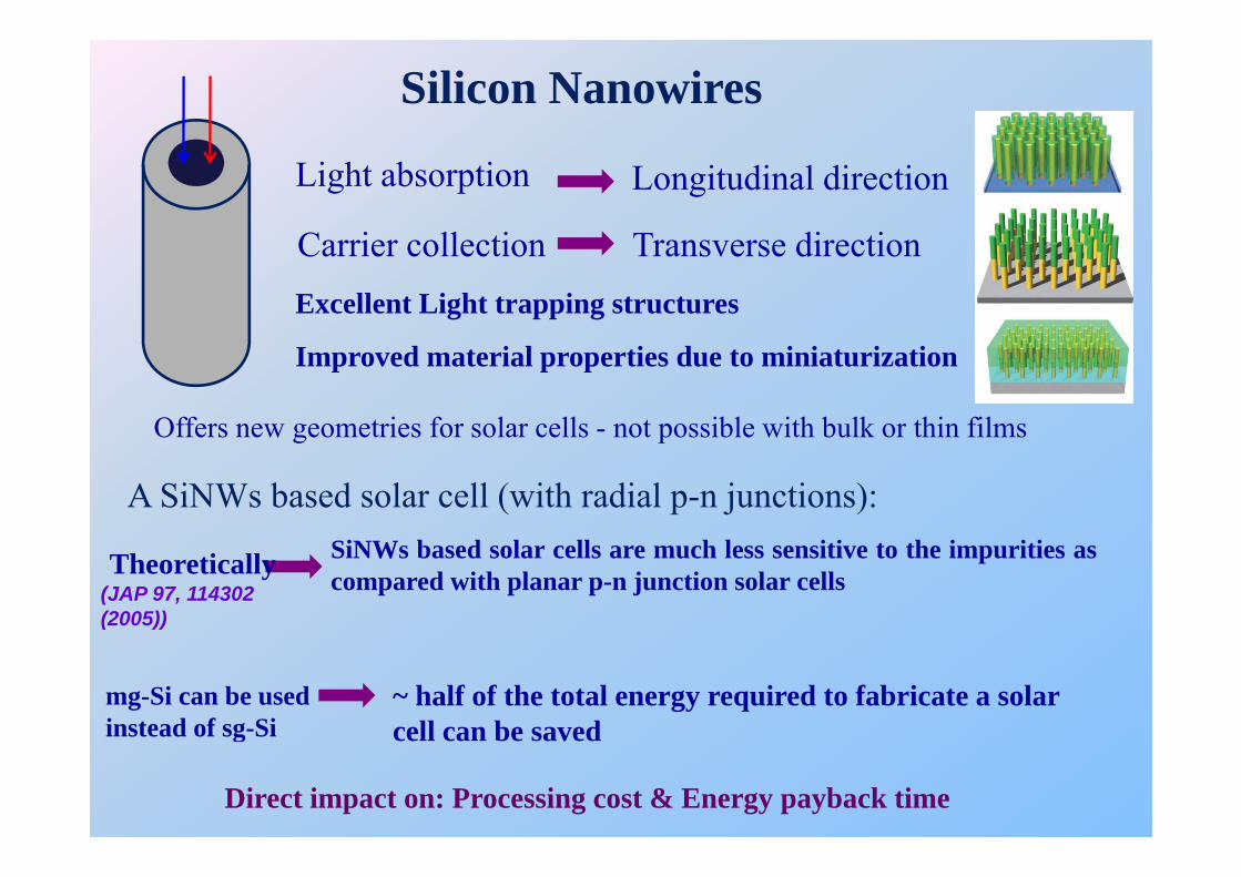
Silicon Nanowires
C i ll ti T di ti
Light absorption Longitudinal direction
Carrier collection Transverse directionExcellent Light trapping structures
Improved material properties due to miniaturization
Offers new geometries for solar cells - not possible with bulk or thin filmsg p
A SiNWs based solar cell (with radial p-n junctions):SiNWs based solar cells are much less sensitive to the impurities ascompared with planar p-n junction solar cellsTheoretically
(JAP 97, 114302 (2005))
mg-Si can be used instead of sg-Si
~ half of the total energy required to fabricate a solar cell can be savedg cell can be saved
Direct impact on: Processing cost & Energy payback time
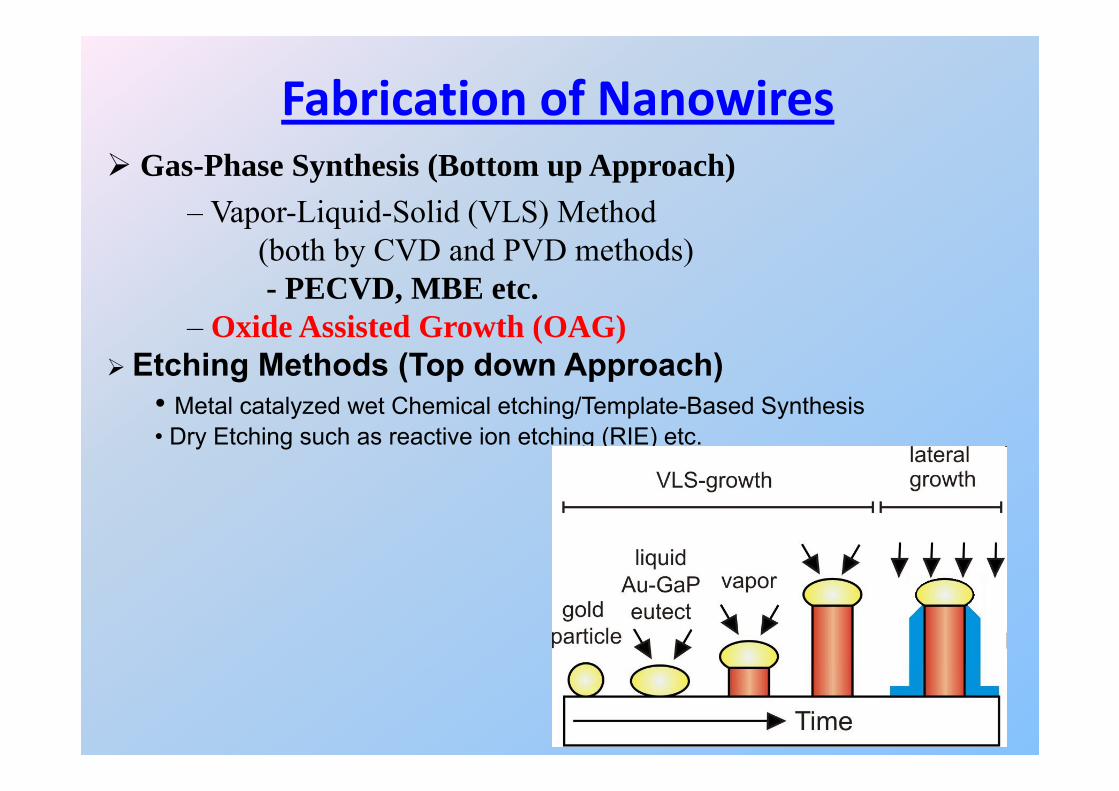
Fabrication of NanowiresGas-Phase Synthesis (Bottom up Approach)
– Vapor-Liquid-Solid (VLS) MethodVapor-Liquid-Solid (VLS) Method (both by CVD and PVD methods)- PECVD, MBE etc.
– Oxide Assisted Growth (OAG)Etching Methods (Top down Approach)
• Metal catalyzed wet Chemical etching/Template-Based Synthesis• Dry Etching such as reactive ion etching (RIE) etc.
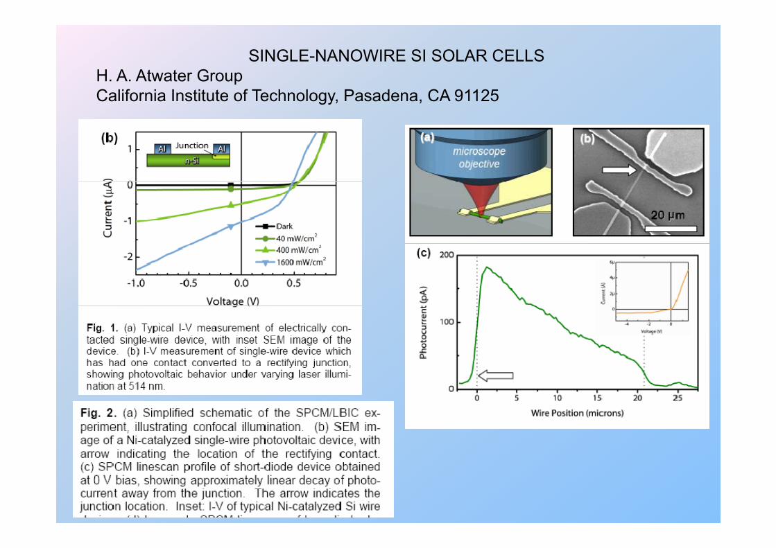
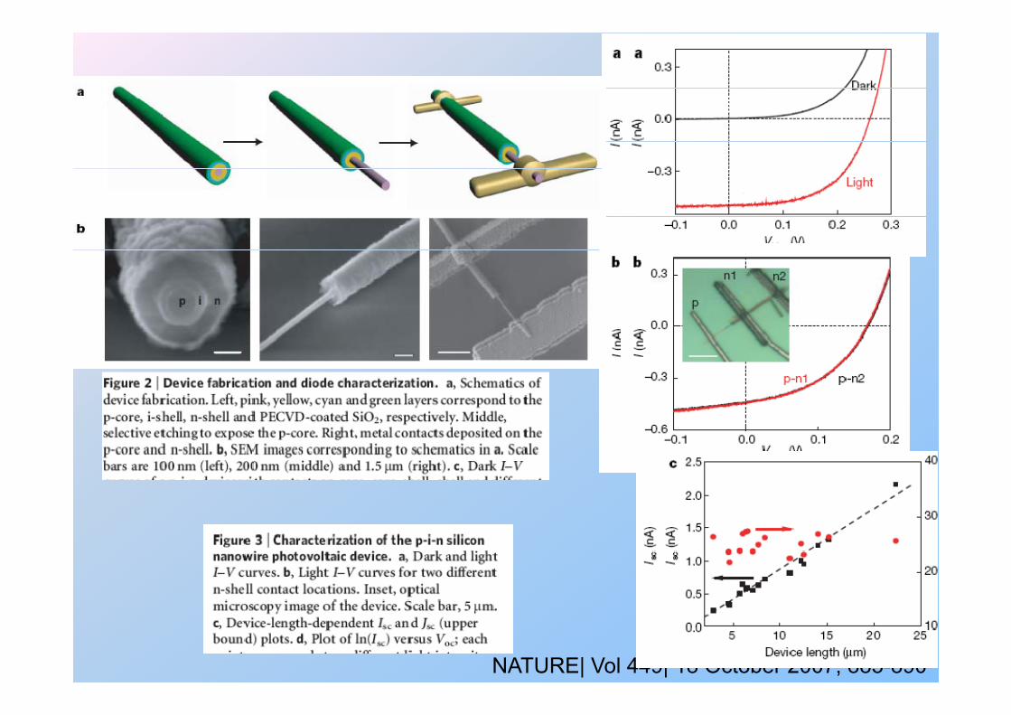
SINGLE-NANOWIRE SI SOLAR CELLSH. A. Atwater GroupCalifornia Institute of Technology, Pasadena, CA 91125
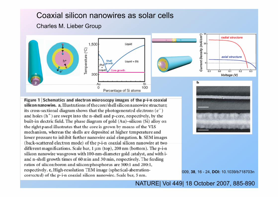
Coaxial silicon nanowires as solar cellsCharles M. Lieber Group
NATURE| Vol 449| 18 October 2007, 885-890
Chem. Soc. Rev., 2009, 38, 16 - 24, DOI: 10.1039/b718703n
NATURE| Vol 449| 18 October 2007, 885-890
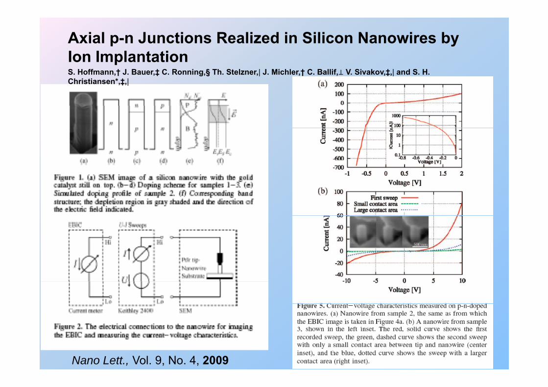
Axial p-n Junctions Realized in Silicon Nanowires by Ion ImplantationIon ImplantationS. Hoffmann,† J. Bauer,‡ C. Ronning,§ Th. Stelzner,| J. Michler,† C. Ballif, V. Sivakov,‡,| and S. H. Christiansen*,‡,|
Nano Lett., Vol. 9, No. 4, 2009
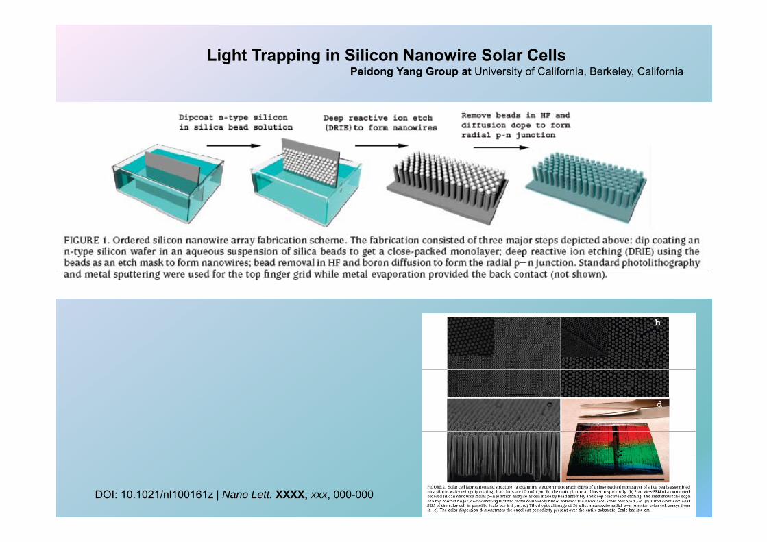
Light Trapping in Silicon Nanowire Solar CellsPeidong Yang Group at University of California, Berkeley, California
DOI: 10.1021/nl100161z | Nano Lett. XXXX, xxx, 000-000
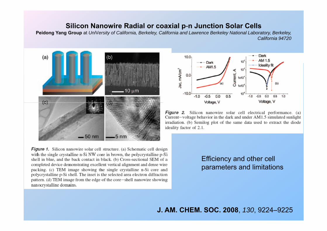
Silicon Nanowire Radial or coaxial p-n Junction Solar CellsPeidong Yang Group at UniVersity of California, Berkeley, California and Lawrence Berkeley National Laboratory, Berkeley,
C lif i 94720California 94720
Efficiency and other cell parameters and limitationsparameters and limitations
J. AM. CHEM. SOC. 2008, 130, 9224–9225
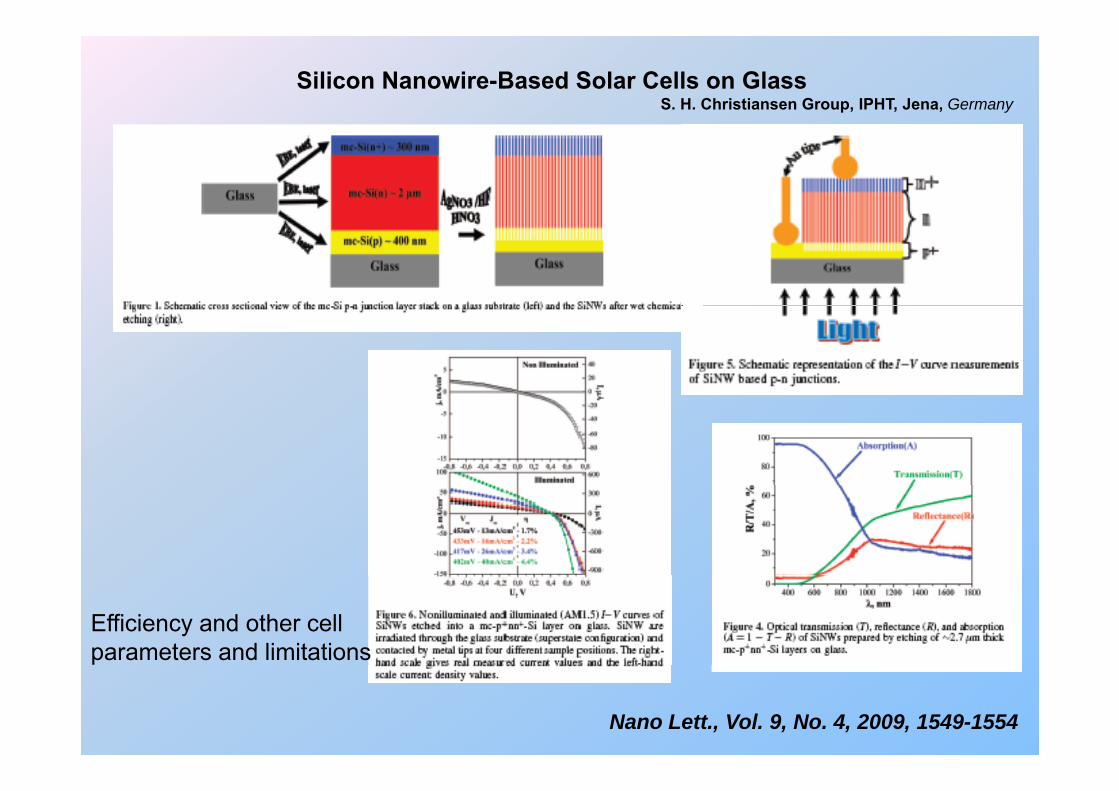
Silicon Nanowire-Based Solar Cells on GlassS. H. Christiansen Group, IPHT, Jena, Germany
Efficiency and other cell parameters and limitations
Nano Lett., Vol. 9, No. 4, 2009, 1549-1554
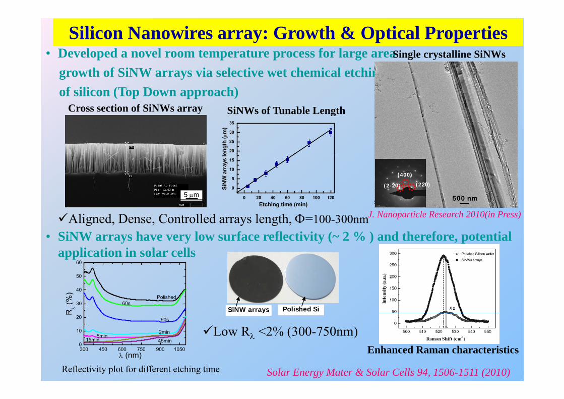
• Developed a novel room temperature process for large area Silicon Nanowires array: Growth & Optical Properties
Single crystalline SiNWs
growth of SiNW arrays via selective wet chemical etching of silicon (Top Down approach)
SiNWs of T nable LengthCross section of SiNWs array
20
25
30
35
engt
h (μ
m)
SiNWs of Tunable LengthCross section of SiNWs array
500 nm
(400)
(220)(2-20)
0 20 40 60 80 100 120
0
5
10
15
SiN
W a
rray
s le
5 μm
• SiNW arrays have very low surface reflectivity (~ 2 % ) and therefore, potential
500 nm
J. Nanoparticle Research 2010(in Press)Etching time (min)
Aligned, Dense, Controlled arrays length, Φ=100-300nm
application in solar cells
40
50
60
SiNW arrays Polished Si
10
20
30
40Polished
5min2min
90s
60s
Rλ (%
)
Low Rλ <2% (300-750nm)300 450 600 750 900 10500
45min15min5min
λ (nm)
Reflectivity plot for different etching time Solar Energy Mater & Solar Cells 94, 1506-1511 (2010)
Low Rλ 2% (300 750nm)Enhanced Raman characteristics
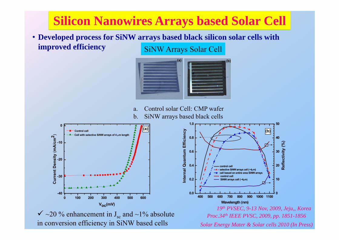
Silicon Nanowires Arrays based Solar Cell • Developed process for SiNW arrays based black silicon solar cells with
Silicon Nanowires Arrays based Solar Cell
(a) (b)
Developed process for SiNW arrays based black silicon solar cells with improved efficiency SiNW Arrays Solar Cell
a. Control solar Cell: CMP waferb. SiNW arrays based black cells
0.8
1.0
Effic
ienc
y
40
50
(%)
(b)
-10
0
A/c
m2 )
Control cell Cell with selective SiNW arrays of 4 μm length
(a)
0.4
0.6
control cell selective SiNW arrays cell (~4μm) cell based on entire area SiNW arraysrn
al Q
uant
um E
20
30
Ref
lect
ivity
-20
ent D
ensi
ty (m
A
400 500 600 700 800 900 1000 11000.0
0.2 control cell SiNW arrays cell (~4μm)
Wavelength (nm)
Inte
r
0
10
0 100 200 300 400 500 600-40
-30
Cur
re
19th PVSEC, 9-13 Nov, 2009, Jeju,, KoreaProc.34th IEEE PVSC, 2009, pp. 1851-1856
Solar Energy Mater & Solar cells 2010 (In Press)
Wavelength (nm)Voc(mV)
~20 % enhancement in Jsc and ~1% absolute in conversion efficiency in SiNW based cells