Four-String, White LED Driver for LCD ... - Analog Devices · Four-String, White LED Driver for LCD...
20
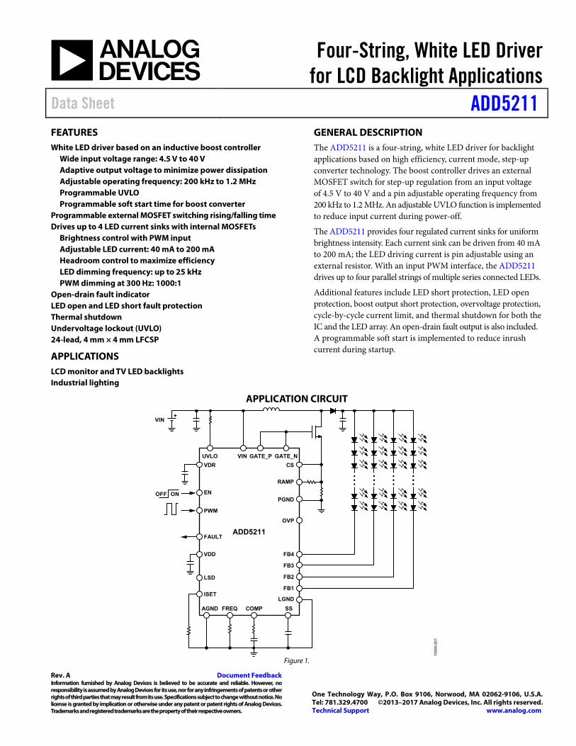
Four-String, White LED Driver for LCD Backlight Applications Data Sheet ADD5211 Rev. A Document Feedback Information furnished by Analog Devices is believed to be accurate and reliable. However, no responsibility is assumed by Analog Devices for its use, nor for any infringements of patents or other rights of third parties that may result from its use. Specifications subject to change without notice. No license is granted by implication or otherwise under any patent or patent rights of Analog Devices. Trademarks and registered trademarks are the property of their respective owners. One Technology Way, P.O. Box 9106, Norwood, MA 02062-9106, U.S.A. Tel: 781.329.4700 ©2013–2017 Analog Devices, Inc. All rights reserved. Technical Support www.analog.com FEATURES White LED driver based on an inductive boost controller Wide input voltage range: 4.5 V to 40 V Adaptive output voltage to minimize power dissipation Adjustable operating frequency: 200 kHz to 1.2 MHz Programmable UVLO Programmable soft start time for boost converter Programmable external MOSFET switching rising/falling time Drives up to 4 LED current sinks with internal MOSFETs Brightness control with PWM input Adjustable LED current: 40 mA to 200 mA Headroom control to maximize efficiency LED dimming frequency: up to 25 kHz PWM dimming at 300 Hz: 1000:1 Open-drain fault indicator LED open and LED short fault protection Thermal shutdown Undervoltage lockout (UVLO) 24-lead, 4 mm × 4 mm LFCSP APPLICATIONS LCD monitor and TV LED backlights Industrial lighting GENERAL DESCRIPTION The ADD5211 is a four-string, white LED driver for backlight applications based on high efficiency, current mode, step-up converter technology. The boost controller drives an external MOSFET switch for step-up regulation from an input voltage of 4.5 V to 40 V and a pin adjustable operating frequency from 200 kHz to 1.2 MHz. An adjustable UVLO function is implemented to reduce input current during power-off. The ADD5211 provides four regulated current sinks for uniform brightness intensity. Each current sink can be driven from 40 mA to 200 mA; the LED driving current is pin adjustable using an external resistor. With an input PWM interface, the ADD5211 drives up to four parallel strings of multiple series connected LEDs. Additional features include LED short protection, LED open protection, boost output short protection, overvoltage protection, cycle-by-cycle current limit, and thermal shutdown for both the IC and the LED array. An open-drain fault output is also included. A programmable soft start is implemented to reduce inrush current during startup. APPLICATION CIRCUIT 10555-001 VIN UVLO GATE_P GATE_N + OFF ON EN ISET LSD VDD FAULT PWM VDR LGND OVP FB4 FB3 FB2 FB1 PGND RAMP CS FREQ COMP AGND SS ADD5211 VIN Figure 1.
Transcript of Four-String, White LED Driver for LCD ... - Analog Devices · Four-String, White LED Driver for LCD...
Four-String, White LED Driver for LCD Backlight Applications
Data Sheet ADD5211
Rev. A Document Feedback Information furnished by Analog Devices is believed to be accurate and reliable. However, no responsibility is assumed by Analog Devices for its use, nor for any infringements of patents or other rights of third parties that may result from its use. Specifications subject to change without notice. No license is granted by implication or otherwise under any patent or patent rights of Analog Devices. Trademarks and registered trademarks are the property of their respective owners.
One Technology Way, P.O. Box 9106, Norwood, MA 02062-9106, U.S.A. Tel: 781.329.4700 ©2013–2017 Analog Devices, Inc. All rights reserved. Technical Support www.analog.com
FEATURES White LED driver based on an inductive boost controller
Wide input voltage range: 4.5 V to 40 V Adaptive output voltage to minimize power dissipation Adjustable operating frequency: 200 kHz to 1.2 MHz Programmable UVLO Programmable soft start time for boost converter
Programmable external MOSFET switching rising/falling time Drives up to 4 LED current sinks with internal MOSFETs
Brightness control with PWM input Adjustable LED current: 40 mA to 200 mA Headroom control to maximize efficiency LED dimming frequency: up to 25 kHz PWM dimming at 300 Hz: 1000:1
Open-drain fault indicator LED open and LED short fault protection Thermal shutdown Undervoltage lockout (UVLO) 24-lead, 4 mm × 4 mm LFCSP
APPLICATIONS LCD monitor and TV LED backlights Industrial lighting
GENERAL DESCRIPTION The ADD5211 is a four-string, white LED driver for backlight applications based on high efficiency, current mode, step-up converter technology. The boost controller drives an external MOSFET switch for step-up regulation from an input voltage of 4.5 V to 40 V and a pin adjustable operating frequency from 200 kHz to 1.2 MHz. An adjustable UVLO function is implemented to reduce input current during power-off.
The ADD5211 provides four regulated current sinks for uniform brightness intensity. Each current sink can be driven from 40 mA to 200 mA; the LED driving current is pin adjustable using an external resistor. With an input PWM interface, the ADD5211 drives up to four parallel strings of multiple series connected LEDs.
Additional features include LED short protection, LED open protection, boost output short protection, overvoltage protection, cycle-by-cycle current limit, and thermal shutdown for both the IC and the LED array. An open-drain fault output is also included. A programmable soft start is implemented to reduce inrush current during startup.
APPLICATION CIRCUIT
1055
5-00
1
VINUVLO GATE_P GATE_N
+
OFF ON EN
ISET
LSD
VDD
FAULT
PWM
VDR
LGND
OVP
FB4
FB3
FB2
FB1
PGND
RAMP
CS
FREQ COMPAGND SS
ADD5211
VIN
Figure 1.

ADD5211 Data Sheet
Rev. A | Page 2 of 20
TABLE OF CONTENTS Features .............................................................................................. 1 Applications ....................................................................................... 1 General Description ......................................................................... 1 Application Circuit ........................................................................... 1 Revision History ............................................................................... 2 Detailed Functional Block Diagram .............................................. 3 Specifications ..................................................................................... 4
General Specifications ................................................................. 4 Step-Up Switching Controller Specifications ........................... 5 LED Current Regulation Specifications .................................... 5
Absolute Maximum Ratings ............................................................ 6 Thermal Resistance ...................................................................... 6 ESD Caution .................................................................................. 6
Pin Configuration and Function Descriptions ..............................7 Typical Performance Characteristics ..............................................8 Theory of Operation ...................................................................... 10
Current Mode, Step-Up Switching Controller ....................... 10 LED Current Regulation ........................................................... 11 Fault Protection .......................................................................... 12
Applications Information .............................................................. 14 Layout Guidelines....................................................................... 14 Boost Component Selection ..................................................... 14
Typical Application Circuits ......................................................... 17 Outline Dimensions ....................................................................... 18
Ordering Guide .......................................................................... 18
REVISION HISTORY 10/2017—Rev. 0 to Rev. A Changed CP-24-7 to CP-24-15 .................................... Throughout Change to Operating Temperature Range (TA), Table 4 ............. 6 Updated Outline Dimensions ....................................................... 18 Changes to Ordering Guide .......................................................... 18 10/2013—Revision 0: Initial Version
Data Sheet ADD5211
Rev. A | Page 3 of 20
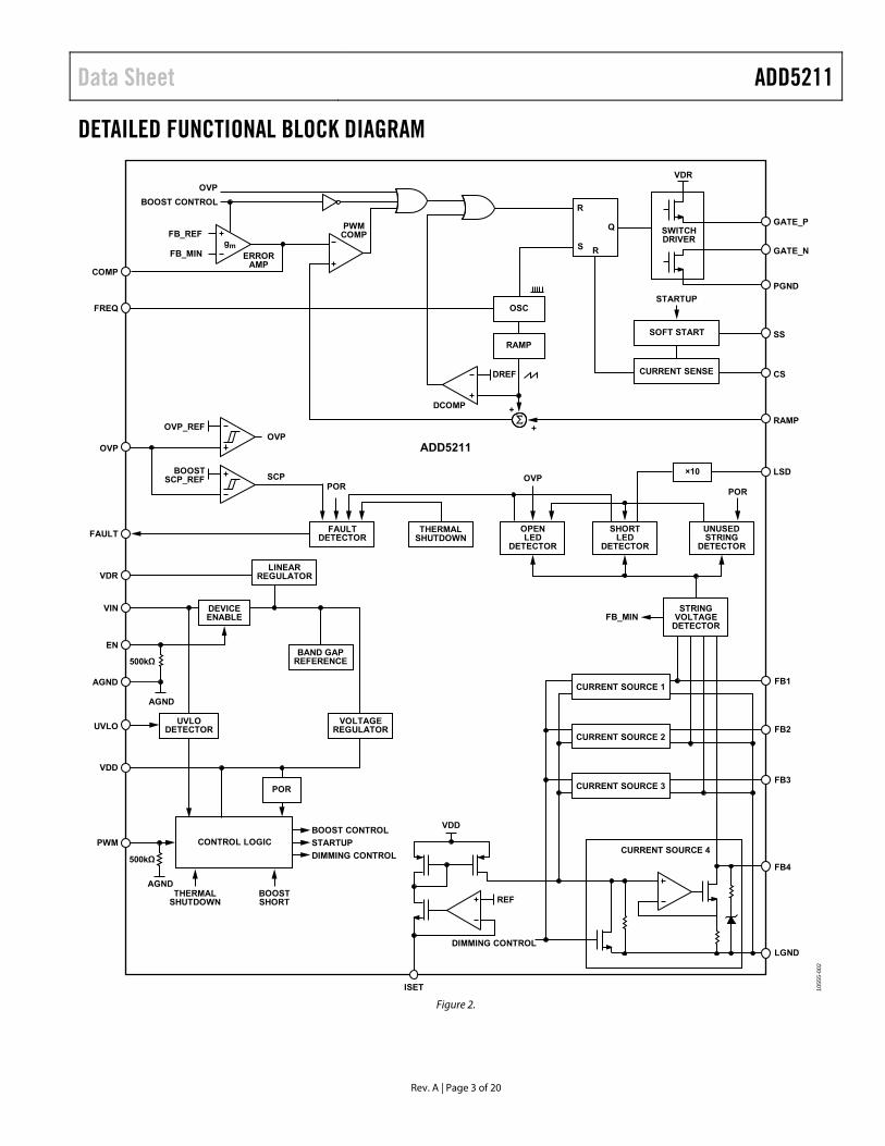
DETAILED FUNCTIONAL BLOCK DIAGRAM
ADD5211
10
555
-00
2
COMP
VIN
EN
UVLO
VDD
PWM
FREQ
AGND
FAULT
OVP
VDR
SS
GATE_P
CS
LGND
LSD
PGND
GATE_N
RAMP
OVP
FB_REF
BOOST CONTROL
FB_MIN ERRORAMP
PWMCOMP
gm
OSC
RAMP
SOFT START
CURRENT SENSE
R
S
Q
R
VDR
SWITCHDRIVER
DCOMP
DREF
+
+
STARTUP
OVP_REFOVP
SCP
FAULTDETECTOR
THERMALSHUTDOWN
POR
OPENLED
DETECTOR
SHORTLED
DETECTOR
UNUSEDSTRING
DETECTOR
OVP
POR
×10
LINEARREGULATOR
BAND GAPREFERENCE
VOLTAGEREGULATOR
POR
UVLODETECTOR
DEVICEENABLE
CONTROL LOGIC STARTUP
BOOST CONTROL
DIMMING CONTROL
DIMMING CONTROL
BOOSTSCP_REF
THERMALSHUTDOWN
BOOSTSHORT
500kΩ
VDD
CURRENT SOURCE 4
FB1
FB2
FB3
FB4
500kΩ
AGND
AGND
STRINGVOLTAGE
DETECTORFB_MIN
CURRENT SOURCE 1
CURRENT SOURCE 2
REF
CURRENT SOURCE 3
ISET Figure 2.

ADD5211 Data Sheet
Rev. A | Page 4 of 20
SPECIFICATIONS VIN = 12 V, EN = 3.3 V, TJ = −40°C to +125°C, unless otherwise noted. Typical values are at TA = 25°C.
GENERAL SPECIFICATIONS
Table 1. Parameter Symbol Test Conditions/Comments Min Typ Max Unit SUPPLY
Input Voltage Range VIN 4.5 40 V Quiescent Current IQ 2.8 6 mA Shutdown Supply Current ISD EN = 0 V 1 µA VIN Rising Threshold VUVLOR_VIN Minimum VIN for startup 4 4.3 V VIN Falling Threshold VUVLOF_VIN 3.2 3.65 V
VDR REGULATOR Regulated Output VVDR_REG 4.75 5.1 5.45 V Dropout Voltage VVDR_DROP VIN = 4.5 V 350 580 mV
VDD REGULATOR Regulated Output VVDD_REG 3.0 3.3 3.6 V
PWM INPUT Input High Voltage VPWM_HIGH 2.2 8 V Input Low Voltage VPWM_LOW 0.8 V PWM Input Current PWM = 5 V 11 30 µA PWM High to LED Turn-On Delay1 1.6 µs PWM Low to LED Turn-Off Delay1 0.8 µs
EN CONTROL EN Voltage High 2.2 17 V EN Voltage Low 0.8 V EN Pin Input Current EN = 5 V 13 30 µA
UNDERVOLTAGE LOCKOUT UVLO Threshold (Rising) 1.10 1.19 1.27 V UVLO Hysteresis 100 mV
FAULT Sink Resistance 40 100 Ω Fault Pin Leakage Current 1.5 µA
LED SHORT DETECTION LED Short Detection Enable Threshold VLSD 2.2 2.5 VDD V LED Short Gain LSD = 1.0 V 7.5 10 13 LED Short Gain Control Range1 0.3 2.0 V
LED FAULT DETECTION DELAY1 LED Open Fault Delay 5 µs LED Short Fault Delay 15 µs
OVERVOLTAGE PROTECTION Overvoltage Threshold (Rising) OVP_REF 2.3 2.5 2.7 V Overvoltage Hysteresis OVP_HYS 100 mV Overvoltage Pin Leakage Current 200 nA Output Short-Circuit Threshold (Falling) VSCPF 100 mV Output Short-Circuit Recovery (Rising) VSCPR 150 mV
THERMAL SHUTDOWN1 Thermal Shutdown Threshold TSD 150 °C Thermal Shutdown Hysteresis TSDHYS 25 °C
1 Guaranteed by design.

Data Sheet ADD5211
Rev. A | Page 5 of 20
STEP-UP SWITCHING CONTROLLER SPECIFICATIONS
Table 2. Parameter Symbol Test Conditions/Comments Min Typ Max Unit BOOST FREQUENCY OSCILLATOR
Switching Frequency Range 200 1200 kHz Switching Frequency fSW RFREQ = 50 kΩ 280 360 430 kHz
PWM COMPARATOR RFREQ = 50 kΩ Maximum Duty Cycle 89 94 98 % Leading Edge Blanking Time 145 ns
CURRENT SENSE LIMIT COMPARATOR Current-Limit Threshold CSLIMIT Independent of duty cycle 275 345 400 mV
SLOPE COMPENSATION Peak Slope Compensation Ramp RRAMP = 5 kΩ 45 µA
ERROR AMPLIFIER Transconductance gm 570 µA/V Output Resistance R 72 MΩ COMP Sink Current 400 µA COMP Source Current 400 µA
MOSFET DRIVER Source Voltage 8 V < VIN < 40 V 5.1 V Gate On Resistance RDS_GATE_P 5.8 Ω Gate Off Resistance RDS_GATE_N 2.4 Ω Rising Time tR C = 1 nF 26 ns Falling Time tF C = 1 nF 21 ns
SOFT START Soft Start Pin Current ISS 2.1 µA
LED CURRENT REGULATION SPECIFICATIONS
Table 3. Parameter Symbol Test Conditions/Comments Min Typ Max Unit CURRENT SINK
Current Sink Range ILED 40 200 mA Current Sink ILED100 RSET = 15 kΩ, TA = 25°C 98 102 mA String-to-String Tolerance1 ΔIFB100 RSET = 15 kΩ, TA = 25°C 0.45 2.5 % Current Accuracy2 ΔILED100 RSET = 15 kΩ, TA = 25°C 2.0 % Minimum Headroom Voltage VHR RSET = 15 kΩ, TA = 25°C 0.4 0.55 0.85 V Off Current IOFF VFB = 40 V, EN = 0 V 1.5 µA Off State Clamping Current ICLAMP VFB = 55 V, EN = 0 V 4 20 80 µA
1 String-to-string tolerance is the greatest delta between FBx currents with respect to the average of the FBx currents.
×
−×
−=∆ %100:%100
LED100
LED100FB100(MIN)
LED100
LED100FB100(MAX)FB100
I
II
I
IIMaxI
where IFB100 is the LED current of each string. 2 Current accuracy is the delta between average current, ILED100, and 100 mA with respect to 100 mA.
%100mA100
mA100×
−=∆ LED100
LED100
II
where
4FB4FB3FB2FB1
LED100IIII
I+++
=

ADD5211 Data Sheet
Rev. A | Page 6 of 20
ABSOLUTE MAXIMUM RATINGS TA = 25°C, unless otherwise noted.
Table 4. Parameter Rating VIN, UVLO −0.3 V to +45 V FB1, FB2, FB3, FB4 −0.3 V to +55 V EN −0.3 V to +17 V PWM, FAULT −0.3 V to +8 V VDR, GATE_N, GATE_P −0.3 V to +7 V COMP, CS, FREQ, ISET, LSD, OVP, RAMP −0.3 V to +3.6 V SS −0.3 V to VDD AGND, PGND, LGND −0.3 V to +0.3 V Maximum Junction Temperature
(TJ max) 150°C
Operating Temperature Range (TA) −40°C to +125°C Storage Temperature Range (TS) −65°C to +150°C Reflow Peak Temperature
(20 sec to 40 sec) 260°C
Stresses at or above those listed under Absolute Maximum Ratings may cause permanent damage to the product. This is a stress rating only; functional operation of the product at these or any other conditions above those indicated in the operational section of this specification is not implied. Operation beyond the maximum operating conditions for extended periods may affect product reliability.
THERMAL RESISTANCE θJA is specified for the worst-case conditions, that is, a device soldered in a circuit board for surface-mount packages.
Table 5. Thermal Resistance Package Type θJA θJC Unit 24-Lead LFCSP 40.5 3.8 °C/W
ESD CAUTION

Data Sheet ADD5211
Rev. A | Page 7 of 20
PIN CONFIGURATION AND FUNCTION DESCRIPTIONS
1055
5-00
3
2
1
3
4
5
6
18
17
16
15
14
13FAULT
PWM
EN
VIN
UVLO
VDR
FB1
FB2
LGND
FB3
FB4
OVP
8 9
10 117
CO
MP
FR
EQ
ISE
T
VD
D
12L
SD
SS
20 1921
RA
MP
PG
ND
CS
22G
AT
E_N
23G
AT
E_P
24A
GN
D
ADD5211TOP VIEW
NOTES1. CONNECT THE EXPOSED PAD TO GROUND.
Figure 3. Pin Configuration
Table 6. Pin Function Descriptions Pin No. Mnemonic Description 1 VDR Switching MOSFET Gate Driver Supply Pin. Bypass VDR to AGND with a 1 μF bypass capacitor. 2 UVLO Input Undervoltage Lockout. Set the start-up and shutdown input voltage level by connecting this pin to the input
voltage with a resistor divider. 3 VIN Supply Input Pin. Bypass VIN to AGND with a 0.1 μF bypass capacitor. 4 EN Shutdown Control Pin for PWM Input Operation Mode. 5 PWM PWM Signal Input. 6 FAULT Open-Drain Fault Output. 7 SS Soft Start Pin. 8 COMP Compensation for the Boost Converter. A capacitor and a resistor are connected in series between ground and this
pin for stable operation. 9 FREQ Frequency Select. A resistor from this pin to ground sets the boost switching frequency from 200 kHz to 1.2 MHz. 10 ISET Full-Scale LED Current Set Pin. A resistor from this pin to ground sets the LED current up to 200 mA. 11 VDD Internal Linear Regulator Output. This regulator provides power to the ADD5211. Bypass VDD to AGND with a 1 μF
bypass capacitor. 12 LSD LED Short Voltage Level Setting Pin. To disable LED short protection, connect this pin to VDD. 13 FB1 Regulated Current Sink. Connect the bottom cathode of the LED string to this pin. If unused, connect FB1 to LGND. 14 FB2 Regulated Current Sink. Connect the bottom cathode of the LED string to this pin. If unused, connect FB2 to LGND. 15 LGND LED Current Sink Ground. 16 FB3 Regulated Current Sink. Connect the bottom cathode of the LED string to this pin. If unused, connect FB3 to LGND. 17 FB4 Regulated Current Sink. Connect the bottom cathode of the LED string to this pin. If unused, connect FB4 to LGND. 18 OVP Overvoltage Protection. The boost converter output is connected to this pin with a resistor divider. 19 PGND Power Ground. 20 RAMP Ramp Compensation Pin. 21 CS Current Sense Input. Allows the current sensing to control the boost converter and to limit the switching current. 22 GATE_N Switching MOSFET Gate Low Driving Pin. 23 GATE_P Switching MOSFET Gate High Driving Pin. 24 AGND Analog Ground. EP Exposed Pad. Connect the exposed pad to ground.

ADD5211 Data Sheet
Rev. A | Page 8 of 20
TYPICAL PERFORMANCE CHARACTERISTICS 110
112
108
104
106
90
88
92
94
96
98
100
102
–35 –25 –15 –5 155 25 35 45 756555 85 95
I LE
D10
0 (
mA
)
TEMPERATURE (°C) 105
55-0
04
Figure 4. ILED100 vs. Temperature
0
5 10 15 20 25 30 35 400 555045
FB
LE
AK
AG
E C
UR
RE
NT
(µ
A)
FB VOLTAGE (V) 105
55-0
06
18
16
14
12
10
8
6
4
20
22
2
TA = –25°C
TA = +85°C
Figure 5. FB Leakage Current vs. FB Voltage
105
55-0
08
1ms/DIV
VSW
30V/DIV
VFB
IFB
20V/DIV
3V/DIV
100mA/DIV
PWM
1
2
3
4
Figure 6. PWM Dimming Waveform, PWM Duty Cycle = 50%
0–35 –25 –15 –5 155 25 35 45 756555 85 95
∆I F
B10
0 (
%)
TEMPERATURE (°C) 105
55-0
05
1.8
1.6
1.4
1.2
1.0
0.8
0.6
0.4
0.2
Figure 7. ΔIFB100 vs. Temperature
6.0
1.50
VD
R V
OL
TA
GE
(V
)
INPUT VOLTAGE (V) 105
55-0
075 10 15 20 25 30 35 40
5.5
5.0
4.5
4.0
3.5
3.0
2.5
2.0
Figure 8. VDR Voltage vs. Input Voltage
105
55-0
09
1ms/DIV
VFB1
20V/DIV
VFB2
VFB4
VFB3
20V/DIV
20V/DIV
20V/DIV
1
2
3
4
Figure 9. FB1 to FB4 Waveforms, PWM Duty Cycle = 50%

Data Sheet ADD5211
Rev. A | Page 9 of 20
1055
5-01
0
20ms/DIV
VSW
30V/DIV
VFB
VIN
EN
20V/DIV
20V/DIV
3V/DIV
1
2
3
4
Figure 10. Startup (Brightness = 100%, EN Is High,
VIN Goes from Low to High)
1055
5-01
2
20ms/DIV
VSW
30V/DIV
VFB
VIN
EN
20V/DIV
20V/DIV
3V/DIV
1
2
3
4
Figure 11. Startup (Brightness = 10%, EN Is High,
VIN Goes from Low to High)
1055
5-01
4
5µs/DIV
VFB1
30V/DIV
PWM
IFB1
3V/DIV
100mA/DIV
2
3
4
Figure 12. LED Current Rising and Falling Waveform
1055
5-01
1
20ms/DIV
VSW
30V/DIV
VFB
VIN
EN
20V/DIV
20V/DIV
3V/DIV
1
2
3
4
Figure 13. Startup (Brightness = 100%, VIN Is High,
EN Goes from Low to High
1055
5-01
3
20ms/DIV
VSW
30V/DIV
VFB
VIN
EN
20V/DIV
20V/DIV
3V/DIV
1
2
3
4
Figure 14. Startup (Brightness = 10%, VIN Is High,
EN Goes from Low to High
1055
5-01
5
1ms/DIV
VOUT
50V/DIV
VFB2
IFB1
FAULT
20V/DIV
100mA/DIV
3V/DIV
1
2
3
4
Figure 15. LED Open Protection (Open LED on FB2)

ADD5211 Data Sheet
Rev. A | Page 10 of 20
THEORY OF OPERATION The ADD5211 uses a PWM boost controller to generate the minimum output voltage required to drive the LED string at the programmed LED current. The current mode control architecture allows a fast transient response while maintaining a stable output voltage. The boost converter provides power to the LED strings, and the four current sinks control the LED current with dynamic headroom control to improve efficiency.
CURRENT MODE, STEP-UP SWITCHING CONTROLLER The ADD5211 is a current mode, PWM boost controller that operates at a fixed switching frequency from 200 kHz to 1.2 MHz. The switching frequency is set by an external resistor connected from the FREQ pin to AGND. The minimum head-room voltage—which is monitored at the FB1, FB2, FB3, and FB4 pins—is compared with the internal reference voltage by the internal transconductance error amplifier to create an error current at COMP. A resistor and capacitor connected from the COMP pin to AGND convert the error current to an error voltage.
At the beginning of the switching cycle, the MOSFET is turned on and the inductor current ramps up. The MOSFET current is measured and converted to a voltage using the current sense resistor (RCS) and is added to the stabilizing slope compensation ramp from the ramp resistor (RRAMP). The resulting voltage sum passes through the current sense amplifier to generate the current sense voltage. Under light loads, the converter can also operate in discontinuous mode with pulse skip modulation to maintain output voltage regulation.
The current mode regulation system of the ADD5211 allows fast transient responses while maintaining a stable output voltage. By selecting the proper resistor-capacitor network from COMP to AGND, the regulator response can be optimized for a wide range of input voltages, output voltages, and load currents.
Input Voltage
The ADD5211 can be powered directly from the VIN pin, which accepts a voltage from 4.5 V to 40 V. The voltage on the VIN pin must exceed VUVLOR_VIN (4.0 V typical) for startup. The ADD5211 has two linear regulators: a 3.3 V linear regulator (VDD), which supplies power to the internal control circuitry, and a 5.1 V linear regulator (VDR), which supplies power to the internal GATE_P and GATE_N drivers.
UVLO Pin
The UVLO pin is used to control the VIN voltage at which the ADD5211 starts up. This function is accomplished using a resistor divider between the input voltage and the UVLO pin, as shown in Figure 16.
VIN
1055
5-01
6
RUVLO1
RUVLO2
UVLO_REF
UVLOPIN
Figure 16. Undervoltage Lockout Circuit
The startup voltage, as determined by the resistor divider to the UVLO pin, can be calculated using the following equation:
VIN(START) = (1.19 V/RUVLO2) × (RUVLO1 + RUVLO2)
To start the device at the lowest possible VIN level, select an RUVLO1 value of 100 kΩ (or greater) and do not connect RUVLO2. If UVLO is controlled from a separate voltage source, make sure that a 100 kΩ (or greater) resistor is in series between the voltage source and the UVLO pin.
Enable and Disable
To enable the ADD5211, the voltage at the EN pin must be higher than 2.2 V. To disable the ADD5211, the voltage at the EN pin must be lower than 0.8 V. An internal 500 kΩ resistor is connected between EN and AGND.
Internal 3.3 V Regulator (VDD)
The ADD5211 contains a 3.3 V linear regulator (VDD) that is used to bias the internal control circuitry. The VDD regulator requires a 1 µF bypass capacitor. Place this bypass capacitor between VDD and AGND, as close as possible to the VDD pin.
Internal 5.1 V Regulator (VDR)
The ADD5211 contains a 5.1 V linear regulator (VDR) that is used to supply the MOSFET gate driver. The VDR regulator requires a 1 µF bypass capacitor. Place this bypass capacitor between VDR and AGND, as close as possible to the VDR pin.

Data Sheet ADD5211
Rev. A | Page 11 of 20
Frequency
The ADD5211 boost converter switching frequency (fSW) is user adjustable from 200 kHz to 1.2 MHz using an external resistor, RFREQ (see Figure 17).
1200
1000
200
0
400
600
800
0 20 40 60 8010 30 50 70 90 100
SWIT
CH
ING
FR
EQU
ENC
Y (k
Hz)
RFREQ (kΩ) 1055
5-01
7
Figure 17. Switching Frequency vs. RFREQ
The following equation can also be used to calculate the typical switching frequency:
2))(k(
000,30
)(k
000,19(kHz)Ω
−Ω
=FREQFREQ
SWRR
f
Soft Start
At startup, the voltage at the SS pin ramps up slowly by charging the soft start capacitor (CSS) from an internal 2.1 μA (typical) current source. The peak inductor current follows the SS pin ramp to provide a controlled start-up profile. The soft start cycle is complete when the SS pin reaches its final value of 1.19 V (typical). A capacitor must always be connected to the SS pin. The soft start time can be calculated as follows:
tSS = (CSS × 1.19 V)/2.1 µA
For a typical setup, a 27 nF soft start capacitor results in negli-gible input current overshoot at startup, making it suitable for most applications. However, if an unusually large output capacitor is used, a longer soft start period is required to prevent input inrush current and output voltage overshoot of the boost switching regu-lator. Conversely, if fast startup is required, the value of the soft start capacitor can be reduced to allow the boost output to start quickly, but allow greater peak switch current during startup and larger boost output overshoot.
LED CURRENT REGULATION Current Sink
The ADD5211 contains four current sinks to provide accurate current sinking for each LED string. The current for each LED string is adjusted from 40 mA to 200 mA using an external resistor. Connect any unused FBx pins to LGND.
If the ADD5211 current sink voltage is greater than 45 V, a Zener diode and a 410 kΩ resistor in parallel with the current sink are activated (see Figure 18).
Programming the LED Current
As shown in Figure 22, the ADD5211 has an LED current set pin (ISET). A resistor (RSET) from the ISET pin to AGND adjusts the LED current from 40 mA to 200 mA. The LED current level can be set using the following equation:
ILED (mA) = 1500/RSET (kΩ)
The resulting minimum current sink voltage (FB_REF) is given by
FB_REF = 0.23 + 0.0041 × ILED (mA)
where 40 mA < ILED < 200 mA.
If only one or two LED strings are used, it is most efficient to connect the FBx pins in parallel and adjust RSET accordingly. This configuration gives the lowest VFB operating voltage and improves efficiency. For example, to drive two LED strings at 100 mA, connect FB1 and FB2 together for one LED string, and connect FB3 and FB4 together for the other LED string. Then, set RSET to 30.1 kΩ (50 mA). The minimum FBx voltage is now 0.44 V (typical) instead of 0.64 V (typical). See Figure 23 for an example of a two-string application.
PWM Dimming Control
The ADD5211 features LED brightness control using an external PWM signal applied at the PWM pin. A logic high signal on the PWM input enables the LED current sinks; a logic low signal disables them. If the PWM input remains low for 50 ms, the ADD5211 stops boost regulation and enters shutdown mode. If the PWM input returns high after the ADD5211 enters shutdown, the device initiates a new soft start sequence.
1055
5-01
8DIMMING CONTROL
CURRENT CONTROL
FBx
LGND
410kΩ
VZ = 45V
Figure 18. Current Sink Circuit
ADD5211 Data Sheet
Rev. A | Page 12 of 20
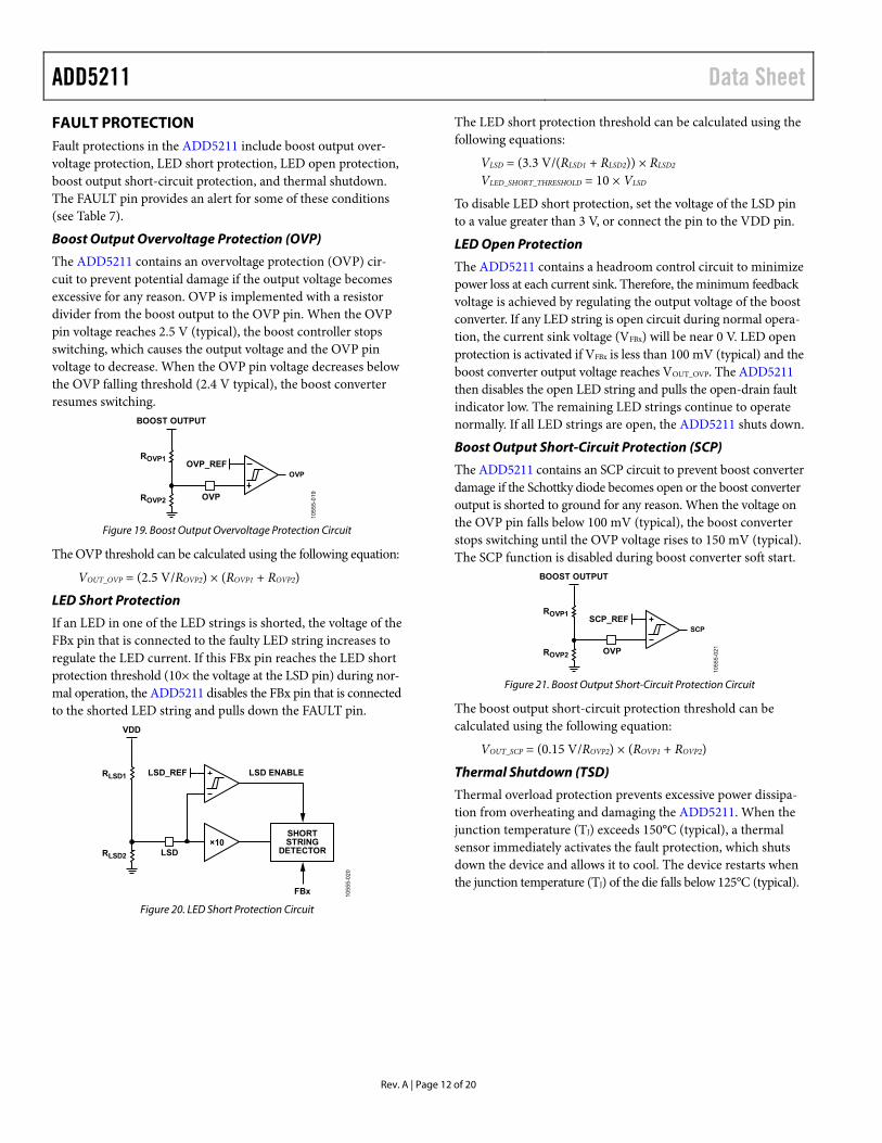
FAULT PROTECTION Fault protections in the ADD5211 include boost output over-voltage protection, LED short protection, LED open protection, boost output short-circuit protection, and thermal shutdown. The FAULT pin provides an alert for some of these conditions (see Table 7).
Boost Output Overvoltage Protection (OVP)
The ADD5211 contains an overvoltage protection (OVP) cir-cuit to prevent potential damage if the output voltage becomes excessive for any reason. OVP is implemented with a resistor divider from the boost output to the OVP pin. When the OVP pin voltage reaches 2.5 V (typical), the boost controller stops switching, which causes the output voltage and the OVP pin voltage to decrease. When the OVP pin voltage decreases below the OVP falling threshold (2.4 V typical), the boost converter resumes switching.
BOOST OUTPUT
1055
5-01
9
ROVP1
ROVP2
OVP_REFOVP
OVP
Figure 19. Boost Output Overvoltage Protection Circuit
The OVP threshold can be calculated using the following equation:
VOUT_OVP = (2.5 V/ROVP2) × (ROVP1 + ROVP2)
LED Short Protection
If an LED in one of the LED strings is shorted, the voltage of the FBx pin that is connected to the faulty LED string increases to regulate the LED current. If this FBx pin reaches the LED short protection threshold (10× the voltage at the LSD pin) during nor-mal operation, the ADD5211 disables the FBx pin that is connected to the shorted LED string and pulls down the FAULT pin.
1055
5-02
0
VDD
RLSD1
RLSD2
LSD_REF LSD ENABLE
SHORTSTRING
DETECTOR
FBx
×10LSD
Figure 20. LED Short Protection Circuit
The LED short protection threshold can be calculated using the following equations:
VLSD = (3.3 V/(RLSD1 + RLSD2)) × RLSD2 VLED_SHORT_THRESHOLD = 10 × VLSD
To disable LED short protection, set the voltage of the LSD pin to a value greater than 3 V, or connect the pin to the VDD pin.
LED Open Protection
The ADD5211 contains a headroom control circuit to minimize power loss at each current sink. Therefore, the minimum feedback voltage is achieved by regulating the output voltage of the boost converter. If any LED string is open circuit during normal opera-tion, the current sink voltage (VFBx) will be near 0 V. LED open protection is activated if VFBx is less than 100 mV (typical) and the boost converter output voltage reaches VOUT_OVP. The ADD5211 then disables the open LED string and pulls the open-drain fault indicator low. The remaining LED strings continue to operate normally. If all LED strings are open, the ADD5211 shuts down.
Boost Output Short-Circuit Protection (SCP)
The ADD5211 contains an SCP circuit to prevent boost converter damage if the Schottky diode becomes open or the boost converter output is shorted to ground for any reason. When the voltage on the OVP pin falls below 100 mV (typical), the boost converter stops switching until the OVP voltage rises to 150 mV (typical). The SCP function is disabled during boost converter soft start.
BOOST OUTPUT
1055
5-02
1
ROVP1
ROVP2
SCP_REFSCP
OVP
Figure 21. Boost Output Short-Circuit Protection Circuit
The boost output short-circuit protection threshold can be calculated using the following equation:
VOUT_SCP = (0.15 V/ROVP2) × (ROVP1 + ROVP2)
Thermal Shutdown (TSD)
Thermal overload protection prevents excessive power dissipa-tion from overheating and damaging the ADD5211. When the junction temperature (TJ) exceeds 150°C (typical), a thermal sensor immediately activates the fault protection, which shuts down the device and allows it to cool. The device restarts when the junction temperature (TJ) of the die falls below 125°C (typical).

Data Sheet ADD5211
Rev. A | Page 13 of 20
Table 7. Fault Protection Fault Description Boost Regulation Response FAULT Pin State Boost output overvoltage VOVP > OVP_REF Stop switching until VOVP < 2.4 V (typical) Open LED string short VFBx > 10 × VLSD; PWM pin is high Shorted LED string disabled; other LED
strings operate normally Pulled down
LED string open VFBx < 0.1 V; VOVP > OVP_REF; PWM pin is high Open LED string disabled; other LED strings operate normally
Pulled down
RSET short to AGND RSET is shorted to AGND ADD5211 shuts down; automatic restart if RSET returns to normal resistance range
Open
Boost output short VOVP < 100 mV (typical) after soft start ADD5211 shuts down; automatic restart if VOVP rises above 150 mV (typical)
Pulled down
Thermal shutdown TJ > 150°C (typical) ADD5211 shuts down; automatic restart after TJ falls below 125°C (typical)
Pulled down

ADD5211 Data Sheet
Rev. A | Page 14 of 20
APPLICATIONS INFORMATION LAYOUT GUIDELINES To achieve high efficiency, good regulation, and stability, a good PCB layout is required. Use the following general guidelines when designing PCBs:
• Ensure that the high current loop from CIN to L1 to Q1 to RCS then back to the ground of CIN is as short as possible.
• Ensure that the high current loop from CIN to L1 to D1 to COUT then back to the ground of CIN is as short as possible.
• Make high current traces as short and wide as possible. • Keep nodes that are connected to L1, Q1, and D1 away
from sensitive traces, such as COMP, to prevent coupling of the traces. If such traces must be run near each other, place a ground trace between the two as a shield.
• Place the compensation components as close as possible to the COMP pin.
• Use thermal vias and a thermal pad with the same dimen-sions as the exposed pad on the bottom of the package.
Heat Sinking
When using a surface-mount power IC or external power switches, the PCB can often be used as the heat sink. This is achieved by using the copper area of the PCB to transfer heat from the device; maximizing this area optimizes thermal performance.
BOOST COMPONENT SELECTION Calculating the Peak Inductor Current and Duty Cycle
To select the optimal external components, the first step is to calculate the peak inductor current and maximum duty cycle. The peak inductor current is given by
IPK = IL (AVG) + (ΔIL/2)
where: ΔIL = (VIN × D)/(L × fSW) IL (AVG) = (4 × ILED)/(η × (1 − D)) ILED is the LED current per string. D is the duty cycle (D = (VOUT − VIN)/VOUT).
Verify that the worst-case duty cycle does not exceed the maxi-mum allowed value (89%) given in Table 2. For the worst-case duty cycle, use the minimum VIN and the maximum VOUT. The maximum VOUT is given by
VOUT_MAX = N × VF MAX + 1 V
where: N is the number of LEDs per string. VF MAX is the maximum LED forward voltage.
Selecting the Inductor
When selecting the inductor, consider these inductor properties: inductance, maximum saturation current, resistance (DCR), and physical size.
Choose an inductance such that ΔIL is 20% to 40% of IL (AVG).
L = OUTSW
IN
If
DDV
××
−××
3.0
)1(
where IOUT is the total LED current through all the strings.
The saturation current is generally listed as the current at which the inductance is reduced by 30%. Ensure that this current is greater than the calculated peak inductor current.
Of the inductors that meet the required inductance and saturation current, choose one that provides the best trade-off between DCR and layout footprint for your application. The power dissipation due to the DCR of the inductor is given by
PL = DCR × IL (AVG)2
Selecting the Current Sense (CS) Resistor
To calculate the worst-case inductor peak current, use the maximum duty cycle, minimum inductance, and minimum switching frequency. Then select the current sense resistor (RCS) as follows:
RCS = CSLIMIT (MIN)/IPK (MAX)
Ensure that the selected inductor can tolerate the maximum peak current given by this current sense resistor.
IPK (CS) = CSLIMIT (MAX)/RCS (MIN)
The power dissipation from the sense resistor is given by
PRCS = D × RCS × IL (AVG)2

Data Sheet ADD5211
Rev. A | Page 15 of 20
Selecting the NMOS Switch
The external NMOS switch must have an adequate drain-to-source breakdown voltage (BVDSS) and rms current rating. The breakdown voltage rating should be at least
BVDSS > VOUT (MAX) + 10 V
The rms current rating should exceed the following:
INMOS (RMS) = IL (AVG) × √D
The power dissipation from the NMOS switch arises from two components: RDSON losses and switching losses. These losses can be calculated as follows:
PNMOS (RDSON) = D × RDSON × IL (AVG)2
PNMOS (SW) = 0.5 × VOUT × IL (AVG) × (tR + tF) × fSW
The rise and fall times (tR and tF) are a function of the strength of the ADD5211 gate drivers and the gate capacitance of the NMOS. Typical values are given in Table 2, but these times vary substantially for various power FETs. Therefore, tR and tF are best measured in the application.
Selecting the Diode
The diode must be selected for a low forward voltage (VF) and fast switching times. Generally, a fast Schottky diode provides the best performance for the cost. Ensure that the breakdown voltage (VD) is greater than the maximum VOUT plus some margin. Also ensure that the rated current of the diode is greater than the output current (total LED current). The power dissipation of the diode is as follows:
PDIODE = VF × IOUT
Selecting COUT
To provide stability and reduce the output voltage ripple, partic-ularly when PWM dimming of the LED currents is in effect, the output capacitance should be in the range of 4.7 µF to 22 µF.
Boost Converter Loop Gain Calculations
The total closed-loop gain is given by GEA × GP (s). GEA is the compensation gain. GP (s) is the control to output gain. GP (s) is the gain of the power stage and includes L, COUT, and the PWM modulator. The GP (s) gain is
GP (s) =
×π×+
×π××+×
×π×+
×π×−×
×π×+
×
2
2
)2(21
21
21
21
nnnLFP
RHPZESRPS
f
s
fQ
s
f
s
f
s
f
s
A
where APS is the dc gain and includes the PWM modulator gain, as follows:
LEDCS
CSOUTPS
IR
GVDA
×××
××−=
42
)1(
The equation for GP (s) shows that there are two zeros (fZESR and fRHP). The fZESR zero is formed by the ESR of the output capacitance. Because ceramic capacitors are used in this application, this value should be small and can usually be ignored. The zero is given by
OUTZESR
CESRf
××π×=
2
1
The right half plane zero (fRHP) is given by 2
42
×
×××π×=
OUT
IN
LED
OUTRHP
V
V
IL
Vf
This RHP zero results in a gain boost, but a phase drop. Because of its dependence on so many variables, fRHP is extremely difficult to compensate for. Therefore, it is best to choose a loop crossover frequency well before the phase drop of this RHP zero is seen. Typically, this is an order of magnitude less than the frequency of the RHP zero.
GP (s) also gives two poles at fLFP and fn. The low frequency pole (fLFP) is formed by the output capacitance and is found at
OUTOUT
LEDLFP
CV
If
××π
×=
4
fn is the double pole formed by the current sense sampling action. It is always located at half the switching frequency.
The fn double pole becomes unstable if Qn (the quality factor) is not sufficiently damped. Qn is damped by adding external ramp compensation (Se).
×−++−×π
=
n
e
n
S
SDD
Q
)1(5.0
1
where: Se is the external ramp compensation = 75% × ((VOUT − VIN)/L). Sn is the inductor up slope = VIN/L.
The external ramp compensation slope is usually set to a value from 50% to 75% of the inductor down slope as reflected across the sense resistor. Given the wide variation in parameters, it is best to stay closer to 75%.
Lf
VVRR
SW
INOUTCSRAMP
××µ
−××=Ω
A45
)(
4
3)(

ADD5211 Data Sheet
Rev. A | Page 16 of 20
Compensation Component Selection
To increase the crossover frequency (beyond the LFP frequency), some kind of phase boost is required. Because the ADD5211 operates in current mode, only one zero is needed to counteract fLFP. Therefore, a Type II compensator should be sufficient. This compensator (see Figure 2) has a gain, GEA, that is expressed as follows:
C
CCm
OUT
FBEA
Cs
CRsg
V
VG
×
+××××=
1
GEA gives one zero and one pole at the origin, as follows:
fzEA = 1/(2π × RC × CC) fpEA = 1/(2π × RO × CC)
where RO is the output impedance of the error amplifier.
To boost the phase and increase the crossover frequency, place the compensation zero (fzEA) at or near the LFP pole. This place-ment gives the following equation for CC:
OUTC
OUTOUTC
IR
CVC
××
×=
2
These values may need to be adjusted experimentally to achieve satisfactory phase margin over all operating conditions and toler-ances. Table 8 provides recommended values for switching frequencies of 360 kHz and 1 MHz.
Table 8. Recommended Values for Compensation Components fSW (kHz) L (µH) COUT (µF) RRAMP (kΩ) RC (Ω) CC (µF) 360 33 10 6.81 100 2.2 1000 22 4.7 6.81 100 1.0
Data Sheet ADD5211
Rev. A | Page 17 of 20
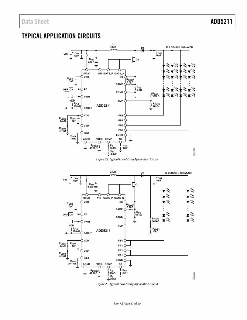
TYPICAL APPLICATION CIRCUITS
1055
5-02
2
RFREQ49.9kΩ
RC100ΩCC2.2µF
CSS30nF
ADD5211
VINUVLO GATE_P GATE_N
+
CIN20.1µF
CIN10µF
COUT10µF
L133µH
RRAMP6.8kΩ
RCS0.1Ω
ROVP1560kΩ
ROVP216kΩ
D1
Q1
CVDR1µF
OFF ON EN
ISET
LSD
VDD
FAULT
PWM
VDR
LGND
OVP
FB4
FB3
FB2
FB1
PGND
RAMP
CS
VDDRFLT100kΩ
RLSD124kΩ
RLSD24.7kΩ
RSET15kΩ FREQ COMPAGND SS
VIN
CVDD1µF
22 LEDs/CH, 100mA/CH
Figure 22. Typical Four-String Application Circuit
RFREQ49.9kΩ
RC100ΩCC2.2µF
CSS30nF
ADD5211
1055
5-02
3
VINUVLO GATE_P GATE_N
+
CIN20.1µF
CIN10µF
COUT10µF
L133µH
RRAMP6.8kΩ
RCS0.1Ω
ROVP1560kΩ
ROVP216kΩ
D1
Q1
CVDR1µF
OFF ON EN
ISET
LSD
VDD
FAULT
PWM
VDR
LGND
OVP
FB4
FB3
FB2
FB1
PGND
RAMP
CS
VDDRFLT100kΩ
RLSD124kΩ
RLSD24.7kΩ
RSET30.1kΩ FREQ COMPAGND SS
VIN
CVDD1µF
22 LEDs/CH, 100mA/CH
Figure 23. Typical Two-String Application Circuit

ADD5211 Data Sheet
Rev. A | Page 18 of 20
OUTLINE DIMENSIONS
0.800.750.70
PK
G-0
04
27
3/5
06
9
0.50BSC
0.500.400.30
COMPLIANT TO JEDEC STANDARDS MO-220-WGGD-8
BOTTOM VIEWTOP VIEW
4.104.00 SQ3.90
0.05 MAX0.02 NOM
0.20 REF
COPLANARITY0.08
PIN 1INDICATOR
1
24
712
13
18
19
6
03-0
2-2
017
-A
0.300.250.18
0.20 MIN
2.702.60 SQ2.50
EXPOSEDPAD
SEATINGPLANE
PIN 1INDIC ATOR AREA OPTIONS(SEE DETAIL A)
DETAIL A(JEDEC 95)
FOR PROPER CONNECTION OFTHE EXPOSED PAD, REFER TOTHE PIN CONFIGURATION ANDFUNCTION DESCRIPTIONSSECTION OF THIS DATA SHEET.
Figure 24. 24-Lead Lead Frame Chip Scale Package [LFCSP]
4 mm × 4 mm Body and 0.75 mm Package Height (CP-24-15)
Dimensions shown in millimeters
ORDERING GUIDE Model1 Temperature Range Package Description Package Option ADD5211ACPZ-R7 −40°C to +125°C 24-Lead LFCSP, 7” Tape and Reel CP-24-15 ADD5211ACPZ-RL −40°C to +125°C 24-Lead LFCSP, 13” Tape and Reel CP-24-15 ADD5211CP-EVALZ Evaluation Board and LED Array AD5211EB-EVALZ Evaluation Board 1 Z = RoHS Compliant Part.

Data Sheet ADD5211
Rev. A | Page 19 of 20
NOTES

ADD5211 Data Sheet
Rev. A | Page 20 of 20
NOTES
©2013–2017 Analog Devices, Inc. All rights reserved. Trademarks and registered trademarks are the property of their respective owners. D10555-0-11/17(A)