Dot Matrix LCD Controller and Driver - Crystalfontz
25
NT3881D Dot Matrix LCD Controller and Driver 1 V2.2 March ,2000 Features Internal LCD drivers 16 common signal drivers 40 segment signal drivers (can be externally extended to 400 segments using NT3882) Maximum display dimensions 40 characters * 2 lines or 80 characters * 1 line Interfaces with 4-bit or 8-bit MPU Versatile display functions provided on chip: Display Clear, Cursor Home, Display ON/OFF, Cursor ON/OFF, Character Blinking, Cursor Shift, and Display Shift Three duty factors, selected by PROGRAM: 1/8, 11/11, and 1/16 Displays Data RAM (DD RAM): 80 X 8 bits (displays up to 80 characters) Character Generator RAM (CG RAM): 64 X 8 bits for general data, 8 5 X 8 programmable dot patterns, or 4 5 X 10 programmable dot patterns Low voltage reset NOVATEK Identification code Bonding option for A-type and B-type waveform Character Generator ROM (CG ROM): 3 kinds of CG ROM sizes: 192 characters: 160 5 X 8 dot patterns 32 5 X 10 dot patterns 240 characters: 192 5 X 8 dot patterns 48 5 X 10 dot patterns 256 characters: 192 5 X 8 dot patterns 64 5 X 10 dot patterns Custom CG ROM is also available Built-in power-on reset function Logic power supply: single +5V supply LCD driver power supply: V1 - V5 (VDD+0.3 - VDD-13.5) Three oscillator operations (Freq. = 250KHz - 270KHz): • Internal oscillation • Ceramic resonator • External clock CMOS Process Available in 80-pin QFP or in CHIP FORM General Description The NT3881D is a dot matrix LCD controller and driver LSI that can operate with either a 4-bit or an 8-bit microprocessor (MPU). NT3881D receives control character codes from the MPU, stores them in an internal RAM (up to 80 characters), transforms each character code into a 5 X 7, 5 X 8, or 5 X 10 dot matrix character pattern, and then displays the codes on the LCD panel. The built-in Character Generator ROM consists of 256 different character patterns. The NT3881D also contains Character Generator RAM where the user can store 8 different character patterns at run time. These memory features make character display flexible. NT3881D also provides many display instructions to achieve versatile LCD display functions. The NT3881D is fabricated on a single LSI chip using the CMOS process, resulting in very low power requirements. With several NT3882 driver ICs connected to the NT3881D, up to 80 characters can be displayed.
Transcript of Dot Matrix LCD Controller and Driver - Crystalfontz
NT3881DDot Matrix LCD Controller and Driver
1 V2.2March ,2000
Features
Internal LCD drivers16 common signal drivers40 segment signal drivers(can be externally extended to 400 segmentsusing NT3882)
Maximum display dimensions40 characters * 2 lines or80 characters * 1 line
Interfaces with 4-bit or 8-bit MPU Versatile display functions provided on chip:
Display Clear, Cursor Home, Display ON/OFF,Cursor ON/OFF, Character Blinking, CursorShift, and Display Shift
Three duty factors, selected by PROGRAM:1/8, 11/11, and 1/16
Displays Data RAM (DD RAM): 80 X 8 bits(displays up to 80 characters)
Character Generator RAM (CG RAM):64 X 8 bits for general data,8 5 X 8 programmable dot patterns, or4 5 X 10 programmable dot patterns
Low voltage reset NOVATEK Identification code Bonding option for A-type and B-type waveform
Character Generator ROM (CG ROM):3 kinds of CG ROM sizes:
192 characters:160 5 X 8 dot patterns32 5 X 10 dot patterns
240 characters:192 5 X 8 dot patterns48 5 X 10 dot patterns
256 characters:192 5 X 8 dot patterns64 5 X 10 dot patterns
Custom CG ROM is also available Built-in power-on reset function Logic power supply: single +5V supply LCD driver power supply: V1 - V5
(VDD+0.3 - VDD-13.5) Three oscillator operations
(Freq. = 250KHz - 270KHz):• Internal oscillation• Ceramic resonator• External clock
CMOS Process Available in 80-pin QFP or in CHIP FORM
General Description
The NT3881D is a dot matrix LCD controller and driverLSI that can operate with either a 4-bit or an 8-bitmicroprocessor (MPU). NT3881D receives controlcharacter codes from the MPU, stores them in aninternal RAM (up to 80 characters), transforms eachcharacter code into a 5 X 7, 5 X 8, or 5 X 10 dot matrixcharacter pattern, and then displays the codes on theLCD panel. The built-in Character Generator ROMconsists of 256 different character patterns.
The NT3881D also contains Character Generator RAMwhere the user can store 8 different character patterns atrun time. These memory features make character displayflexible. NT3881D also provides many displayinstructions to achieve versatile LCD display functions.The NT3881D is fabricated on a single LSI chip using theCMOS process, resulting in very low powerrequirements.With several NT3882 driver ICs connected to theNT3881D, up to 80 characters can be displayed.
NT3881D
2
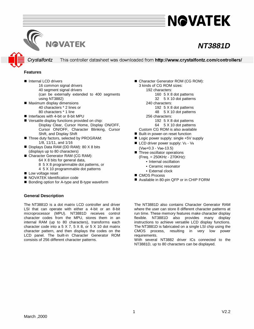
Pin Configuration
UM3881DFNT3881DF
SEG21
SEG20
SEG19
SEG18
SEG17
SEG16
SEG15
SEG14
SEG13
SEG12
SEG11
SEG10
SEG9
SEG8
SEG7
SEG6
SEG5
SEG4
SEG3
SEG2
SEG1
GND
OSC1
SEG23
SEG24
SEG25
SEG26
SEG27
SEG28
SEG29
SEG30
SEG31
SEG32
SEG33
SEG34
SEG35
SEG36
SEG37
SEG38 DB1
DB0
E
R/W
RS
D
M
VDD
CL2
CL1
V5
V4
V3
V2
V1
OSC2
SEG22
SEG39
SEG40
COM16
COM15
COM14
COM13
COM12
COM11
COM10
COM9
COM8
COM7
COM6
COM5
COM4
COM3
COM2
COM1
DB7
DB6
DB5
DB4
DB3
DB2
64 63 62 61 60 59 58 57 56 55 54 53 52 51 50 49 48 47 46 45 44 43 42 41
65
66
67
68
69
70
71
72
73
74
75
76
77
78
79
80
1 2 3 4 5 6 7 8 9 10 11 12 13 14 15 16 17 18 19 20 21 22 23 24
40
39
38
37
36
35
34
33
32
31
30
29
28
27
26
25
NT3881D
3
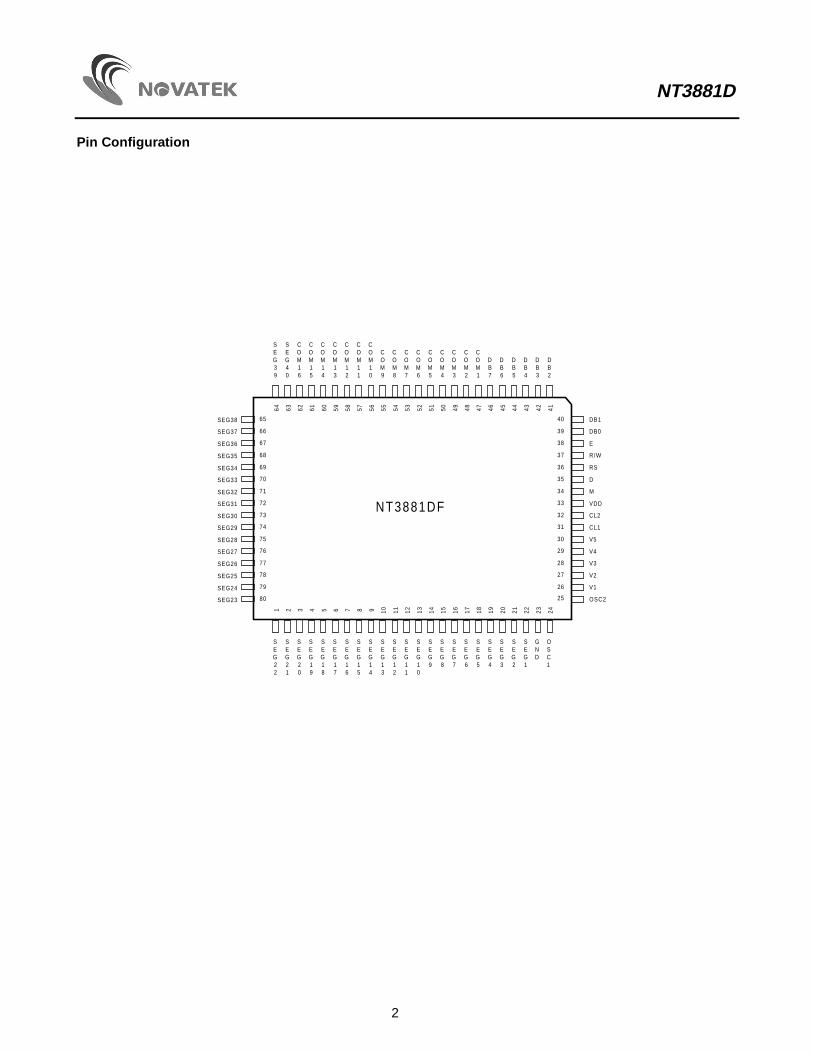
Pad Configuration
1
2
3
4
5
6
7
8
9
1 0
1 1
1 2
1 3
1 4
1 5
1 6
1 7
1 8
1 9
2 0
2 1
2 2
2 3
2 4
2 5 2 6 2 7 2 8 2 9 3 0 3 1 3 28 1
3 4 3 5 3 6 3 7 3 8 3 9 4 0
4 1
4 2
4 3
4 4
4 5
4 6
4 7
4 8
4 9
5 0
5 1
5 2
5 3
5 4
5 5
5 6
5 7
5 8
5 9
6 0
6 1
6 2
6 3
6 4
6 56 76 86 97 07 17 27 37 47 57 67 77 87 98 0
NT3881DH
6 6
3 3
S E G 2 2
S E G 2 1
S E G 2 0
S E G 1 9
S E G 1 8
S E G 1 7
S E G 1 6
S E G 1 5
S E G 1 4
S E G 1 3
S E G 1 2
S E G 1 1
S E G 1 0
S E G 9
S E G 8
S E G 7
S E G 6
S E G 5
S E G 4
S E G 3
S E G 2
S E G 1
G N D
O S C 1
S E G 3 9
S E G 4 0
C O M 16C O M 15C O M 14C O M 13C O M 12C O M 11C O M 10
C O M 9
C O M 8
C O M 7
C O M 6
C O M 5
C O M 4
C O M 3
C O M 2
C O M 1
D B 7
D B 6
D B 5
D B 4
D B 3
D B 2
OSC2
V1
V2
V3
V4
V5
CL1
CL2
VDDA
M D RS
R/W
E DB0
DB1
VDDB
SEG23
SEG24
SEG25
SEG26
SEG27
SEG28
SEG29
SEG30
SEG31
SEG32
SEG33
SEG34
SEG35
SEG36
SEG37
SEG38
NT3881D
4
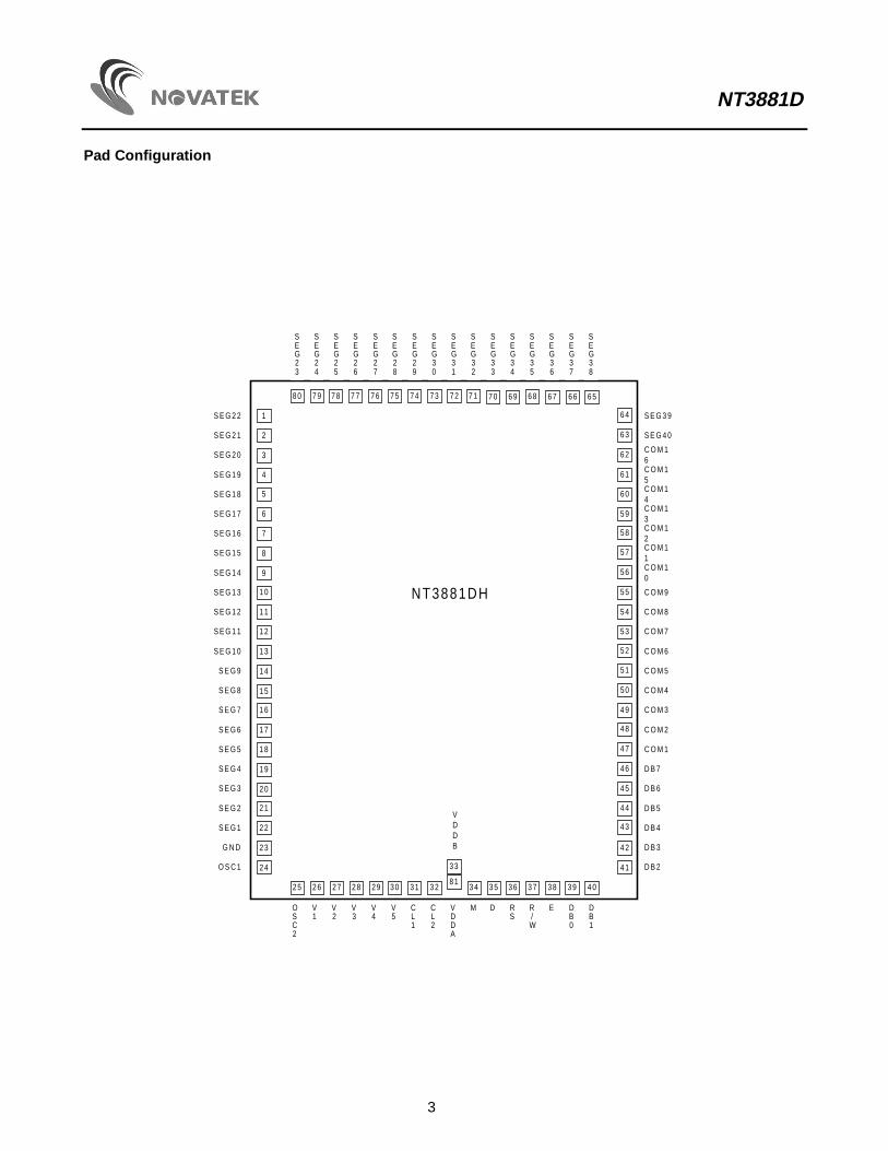
Block Diagram
NT3881D
5
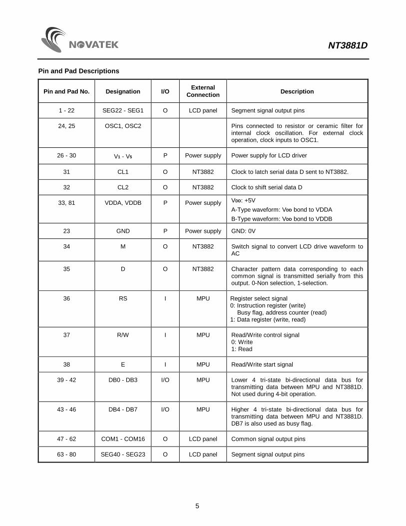
Pin and Pad Descriptions
Pin and Pad No. Designation I/OExternal
Connection Description
1 - 22 SEG22 - SEG1 O LCD panel Segment signal output pins
24, 25 OSC1, OSC2 Pins connected to resistor or ceramic filter forinternal clock oscillation. For external clockoperation, clock inputs to OSC1.
26 - 30 V1 - V5 P Power supply Power supply for LCD driver
31 CL1 O NT3882 Clock to latch serial data D sent to NT3882.
32 CL2 O NT3882 Clock to shift serial data D
33, 81 VDDA, VDDB P Power supply VDD: +5V
A-Type waveform: VDD bond to VDDA
B-Type waveform: VDD bond to VDDB
23 GND P Power supply GND: 0V
34 M O NT3882 Switch signal to convert LCD drive waveform toAC
35 D O NT3882 Character pattern data corresponding to eachcommon signal is transmitted serially from thisoutput. 0-Non selection, 1-selection.
36 RS I MPU Register select signal0: Instruction register (write) Busy flag, address counter (read)1: Data register (write, read)
37 R/W I MPU Read/Write control signal0: Write1: Read
38 E I MPU Read/Write start signal
39 - 42 DB0 - DB3 I/O MPU Lower 4 tri-state bi-directional data bus fortransmitting data between MPU and NT3881D.Not used during 4-bit operation.
43 - 46 DB4 - DB7 I/O MPU Higher 4 tri-state bi-directional data bus fortransmitting data between MPU and NT3881D.DB7 is also used as busy flag.
47 - 62 COM1 - COM16 O LCD panel Common signal output pins
63 - 80 SEG40 - SEG23 O LCD panel Segment signal output pins
NT3881D
6
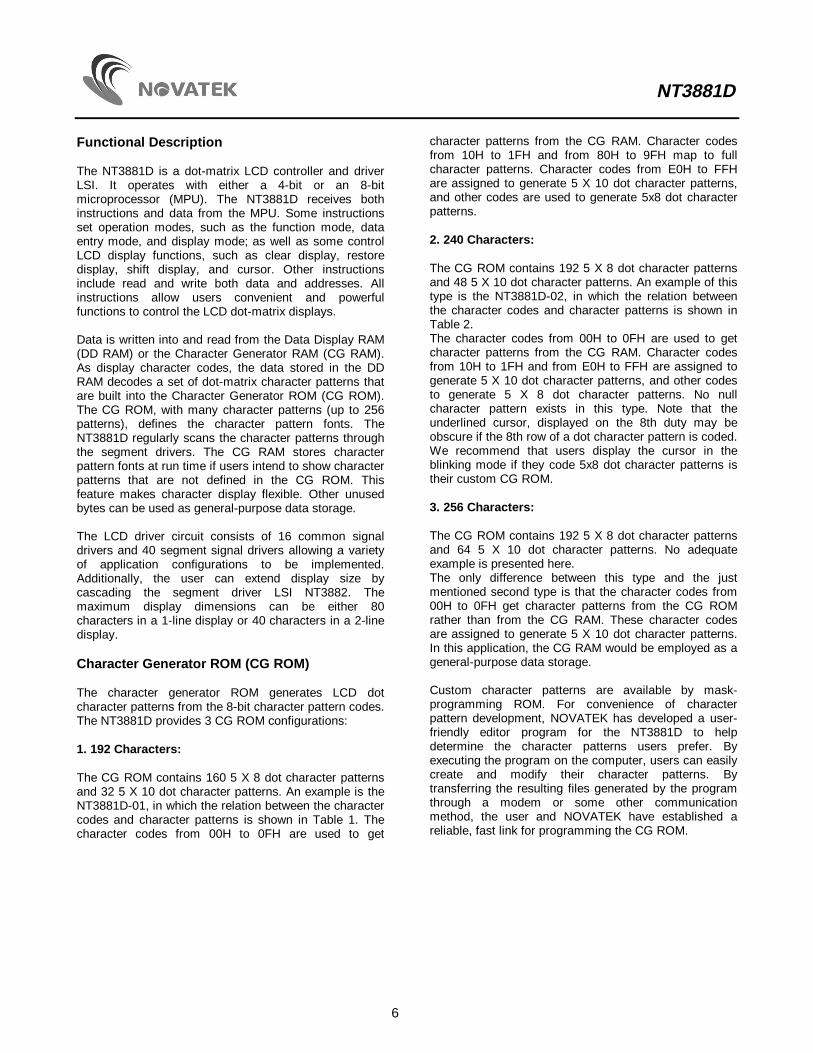
Functional D escription
The NT3881D is a dot-matrix LCD controller and driverLSI. It operates with either a 4-bit or an 8-bitmicroprocessor (MPU). The NT3881D receives bothinstructions and data from the MPU. Some instructionsset operation modes, such as the function mode, dataentry mode, and display mode; as well as some controlLCD display functions, such as clear display, restoredisplay, shift display, and cursor. Other instructionsinclude read and write both data and addresses. Allinstructions allow users convenient and powerfulfunctions to control the LCD dot-matrix displays.
Data is written into and read from the Data Display RAM(DD RAM) or the Character Generator RAM (CG RAM).As display character codes, the data stored in the DDRAM decodes a set of dot-matrix character patterns thatare built into the Character Generator ROM (CG ROM).The CG ROM, with many character patterns (up to 256patterns), defines the character pattern fonts. TheNT3881D regularly scans the character patterns throughthe segment drivers. The CG RAM stores characterpattern fonts at run time if users intend to show characterpatterns that are not defined in the CG ROM. Thisfeature makes character display flexible. Other unusedbytes can be used as general-purpose data storage.
The LCD driver circuit consists of 16 common signaldrivers and 40 segment signal drivers allowing a varietyof application configurations to be implemented.Additionally, the user can extend display size bycascading the segment driver LSI NT3882. Themaximum display dimensions can be either 80characters in a 1-line display or 40 characters in a 2-linedisplay.
Character Generator ROM (CG ROM)
The character generator ROM generates LCD dotcharacter patterns from the 8-bit character pattern codes.The NT3881D provides 3 CG ROM configurations:
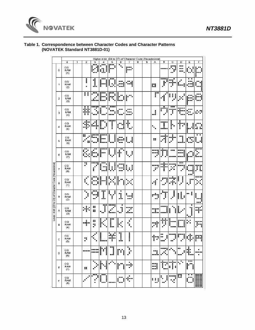
1. 192 Characters:
The CG ROM contains 160 5 X 8 dot character patternsand 32 5 X 10 dot character patterns. An example is theNT3881D-01, in which the relation between the charactercodes and character patterns is shown in Table 1. Thecharacter codes from 00H to 0FH are used to get
character patterns from the CG RAM. Character codesfrom 10H to 1FH and from 80H to 9FH map to fullcharacter patterns. Character codes from E0H to FFHare assigned to generate 5 X 10 dot character patterns,and other codes are used to generate 5x8 dot characterpatterns.
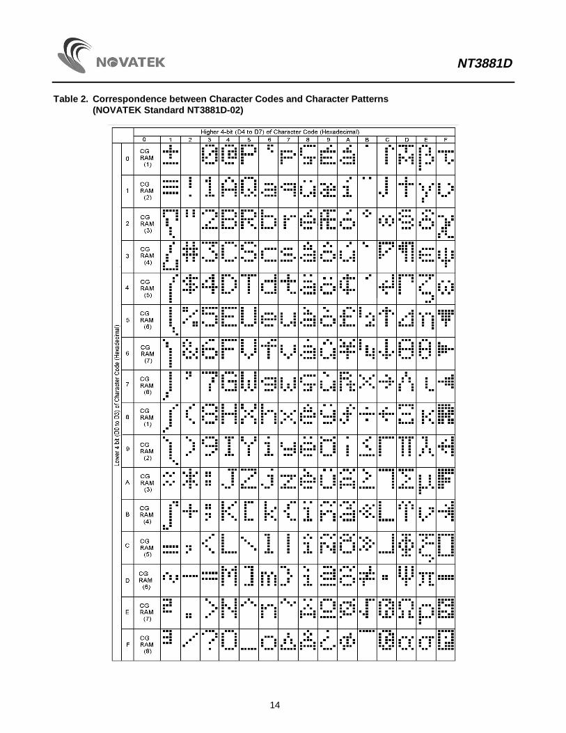
2. 240 Characters:
The CG ROM contains 192 5 X 8 dot character patternsand 48 5 X 10 dot character patterns. An example of thistype is the NT3881D-02, in which the relation betweenthe character codes and character patterns is shown inTable 2.The character codes from 00H to 0FH are used to getcharacter patterns from the CG RAM. Character codesfrom 10H to 1FH and from E0H to FFH are assigned togenerate 5 X 10 dot character patterns, and other codesto generate 5 X 8 dot character patterns. No nullcharacter pattern exists in this type. Note that theunderlined cursor, displayed on the 8th duty may beobscure if the 8th row of a dot character pattern is coded.We recommend that users display the cursor in theblinking mode if they code 5x8 dot character patterns istheir custom CG ROM.
3. 256 Characters:
The CG ROM contains 192 5 X 8 dot character patternsand 64 5 X 10 dot character patterns. No adequateexample is presented here.The only difference between this type and the justmentioned second type is that the character codes from00H to 0FH get character patterns from the CG ROMrather than from the CG RAM. These character codesare assigned to generate 5 X 10 dot character patterns.In this application, the CG RAM would be employed as ageneral-purpose data storage.
Custom character patterns are available by mask-programming ROM. For convenience of characterpattern development, NOVATEK has developed a user-friendly editor program for the NT3881D to helpdetermine the character patterns users prefer. Byexecuting the program on the computer, users can easilycreate and modify their character patterns. Bytransferring the resulting files generated by the programthrough a modem or some other communicationmethod, the user and NOVATEK have established areliable, fast link for programming the CG ROM.
NT3881D
7
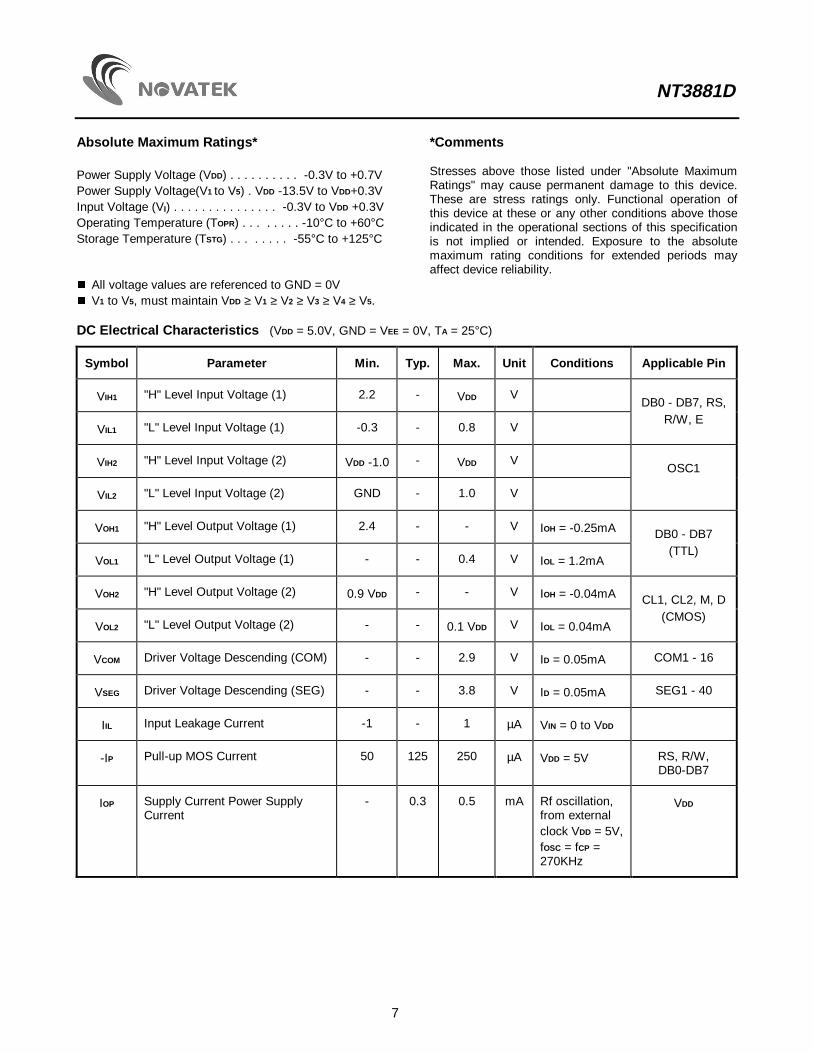
Absolute Maximum Ratings*
Power Supply Voltage (VDD) . . . . . . . . . . -0.3V to +0.7VPower Supply Voltage(V1 to V5) . VDD -13.5V to VDD+0.3VInput Voltage (VI) . . . . . . . . . . . . . . . -0.3V to VDD +0.3VOperating Temperature (TOPR) . . . . . . . . -10°C to +60°CStorage Temperature (TSTG) . . . . . . . . -55°C to +125°C
*Comments
Stresses above those listed under "Absolute MaximumRatings" may cause permanent damage to this device.These are stress ratings only. Functional operation ofthis device at these or any other conditions above thoseindicated in the operational sections of this specificationis not implied or intended. Exposure to the absolutemaximum rating conditions for extended periods mayaffect device reliability.
All voltage values are referenced to GND = 0V V1 to V5, must maintain VDD ≥ V1 ≥ V2 ≥ V3 ≥ V4 ≥ V5.
DC Electrical Characteristics (VDD = 5.0V, GND = VEE = 0V, TA = 25°C)
Symbol Parameter Min. Typ. Max. Unit Conditions Applicable Pin
VIH1 "H" Level Input Voltage (1) 2.2 - VDD VDB0 - DB7, RS,
VIL1 "L" Level Input Voltage (1) -0.3 - 0.8 VR/W, E
VIH2 "H" Level Input Voltage (2) VDD -1.0 - VDD VOSC1
VIL2 "L" Level Input Voltage (2) GND - 1.0 V
VOH1 "H" Level Output Voltage (1) 2.4 - - V IOH = -0.25mA DB0 - DB7
VOL1 "L" Level Output Voltage (1) - - 0.4 V IOL = 1.2mA(TTL)
VOH2 "H" Level Output Voltage (2) 0.9 VDD - - V IOH = -0.04mA CL1, CL2, M, D
VOL2 "L" Level Output Voltage (2) - - 0.1 VDD V IOL = 0.04mA(CMOS)
VCOM Driver Voltage Descending (COM) - - 2.9 V ID = 0.05mA COM1 - 16
VSEG Driver Voltage Descending (SEG) - - 3.8 V ID = 0.05mA SEG1 - 40
IIL Input Leakage Current -1 - 1 µA VIN = 0 to VDD
-IP Pull-up MOS Current 50 125 250 µA VDD = 5V RS, R/W,DB0-DB7
IOP Supply Current Power SupplyCurrent
- 0.3 0.5 mA Rf oscillation,from externalclock VDD = 5V,fOSC = fCP =270KHz
VDD
NT3881D
8
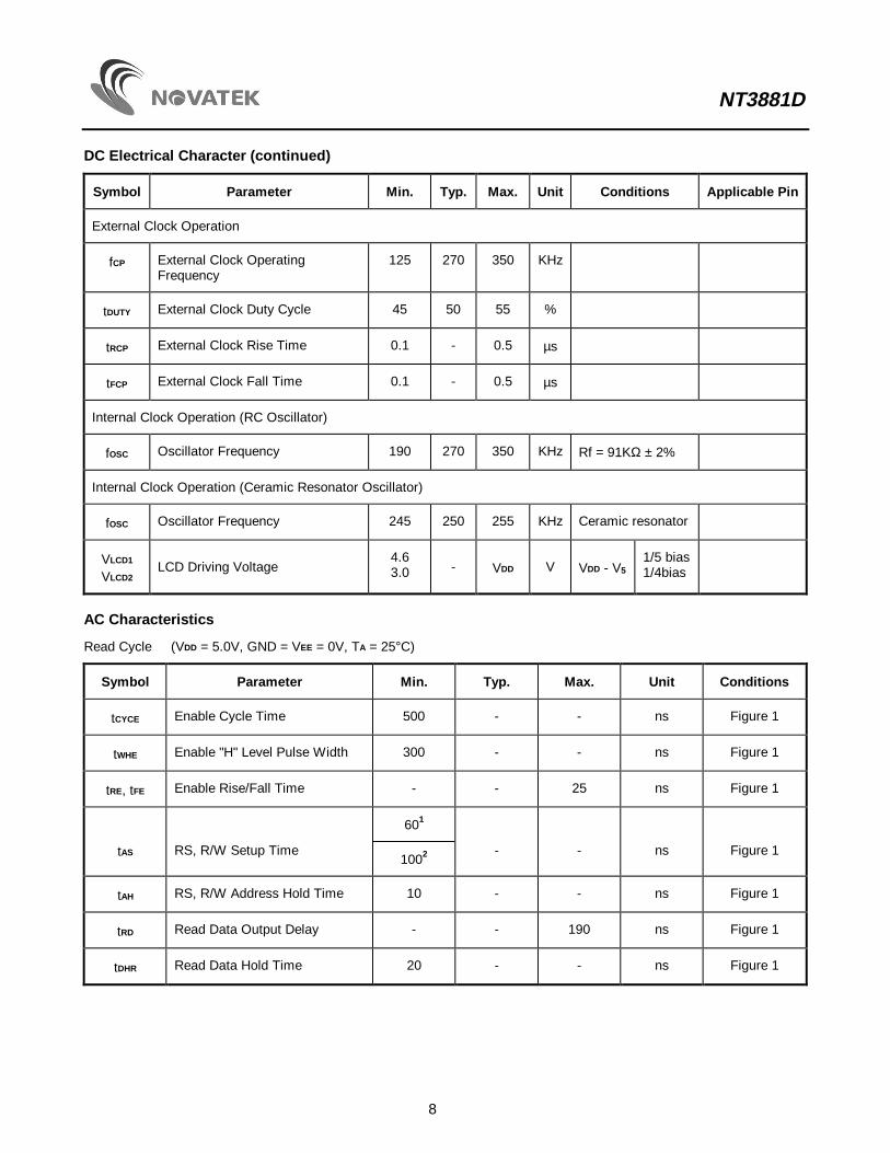
DC Electrical Character (continued)
Symbol Parameter Min. Typ. Max. Unit Conditions Applicable Pin
External Clock Operation
fCP External Clock OperatingFrequency
125 270 350 KHz
tDUTY External Clock Duty Cycle 45 50 55 %
tRCP External Clock Rise Time 0.1 - 0.5 µs
tFCP External Clock Fall Time 0.1 - 0.5 µs
Internal Clock Operation (RC Oscillator)
fOSC Oscillator Frequency 190 270 350 KHz Rf = 91KΩ ± 2%
Internal Clock Operation (Ceramic Resonator Oscillator)
fOSC Oscillator Frequency 245 250 255 KHz Ceramic resonator
VLCD1
VLCD2LCD Driving Voltage
4.63.0 - VDD V VDD - V5
1/5 bias1/4bias
AC Characteristics
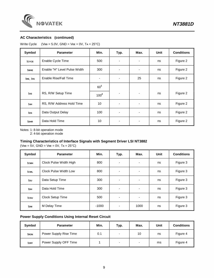
Read Cycle (VDD = 5.0V, GND = VEE = 0V, TA = 25°C)
Symbol Parameter Min. Typ. Max. Unit Conditions
tCYCE Enable Cycle Time 500 - - ns Figure 1
tWHE Enable "H" Level Pulse Width 300 - - ns Figure 1
tRE, tFE Enable Rise/Fall Time - - 25 ns Figure 1
601
tAS RS, R/W Setup Time1002 - - ns Figure 1
tAH RS, R/W Address Hold Time 10 - - ns Figure 1
tRD Read Data Output Delay - - 190 ns Figure 1
tDHR Read Data Hold Time 20 - - ns Figure 1
NT3881D
9
AC Characteristics (continued)
Write Cycle (VDD = 5.0V, GND = VEE = 0V, TA = 25°C)
Symbol Parameter Min. Typ. Max. Unit Conditions
tCYCE Enable Cycle Time 500 - - ns Figure 2
tWHE Enable "H" Level Pulse Width 300 - - ns Figure 2
tRE, tFE Enable Rise/Fall Time - - 25 ns Figure 2
601
tAS RS, R/W Setup Time1002 - - ns Figure 2
tAH RS, R/W Address Hold Time 10 - - ns Figure 2
tDS Data Output Delay 100 - - ns Figure 2
tDHR Data Hold Time 10 - - ns Figure 2
Notes: 1: 8-bit operation mode2: 4-bit operation mode
Timing Characteristics of Interface Signals with Segment Driver LSI NT3882(VDD = 5V, GND = VEE = 0V, TA = 25°C)
Symbol Parameter Min. Typ. Max. Unit Conditions
tCWH Clock Pulse Width High 800 - - ns Figure 3
tCWL Clock Pulse Width Low 800 - - ns Figure 3
tSU Data Setup Time 300 - - ns Figure 3
tDH Data Hold Time 300 - - ns Figure 3
tCSU Clock Setup Time 500 - - ns Figure 3
tDM M Delay Time -1000 - 1000 ns Figure 3
Power Supply Conditions Using Internal R eset Circuit
Symbol Parameter Min. Typ. Max. Unit Conditions
tRON Power Supply Rise Time 0.1 - 10 ns Figure 4
tOFF Power Supply OFF Time 1 - - ms Figure 4
NT3881D
10
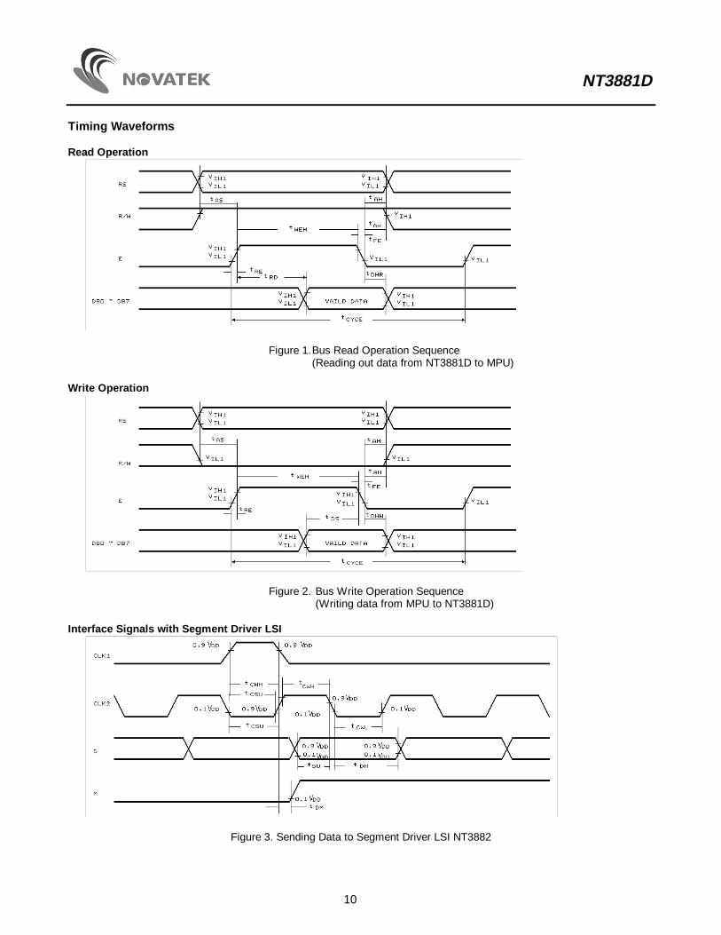
Timing Waveforms
Read Operation
Figure 1.Bus Read Operation Sequence(Reading out data from NT3881D to MPU)
Write Operation
Figure 2. Bus Write Operation Sequence(Writing data from MPU to NT3881D)
Interface Signals with Segment Driver LSI
Figure 3. Sending Data to Segment Driver LSI NT3882
NT3881D
11
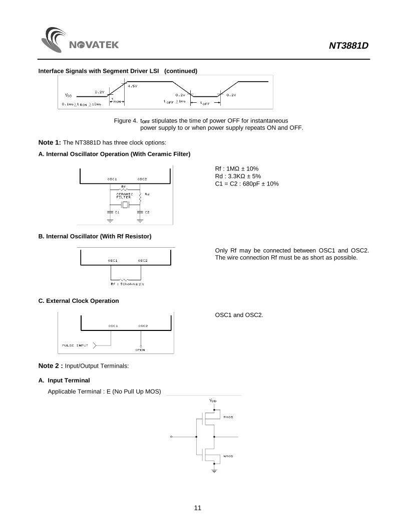
Interface Signals with Segment Driver LSI (continued)
Figure 4. tOFF stipulates the time of power OFF for instantaneouspower supply to or when power supply repeats ON and OFF.
Note 1: The NT3881D has three clock options:
A. Internal Oscillator Operation (With Ceramic Filter)
Rf : 1MΩ ± 10%Rd : 3.3KΩ ± 5%C1 = C2 : 680pF ± 10%
B. Internal Oscillator (With Rf Resistor)
Only Rf may be connected between OSC1 and OSC2.The wire connection Rf must be as short as possible.
C. External Clock Operation
OSC1 and OSC2.
Note 2 : Input/Output Terminals:
A. Input Terminal
Applicable Terminal : E (No Pull Up MOS)
NT3881D
12
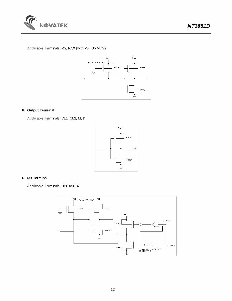
Applicable Terminals: RS, R/W (with Pull Up MOS)
B. Output Terminal
Applicable Terminals: CL1, CL2, M, D
C. I/O Terminal
Applicable Terminals: DB0 to DB7
NT3881D
13
Table 1. Correspondence between Character Codes and Character Patterns(NOVATEK Standard NT3881D-01)
NT3881D
14
Table 2. Correspondence between Character Codes and Character Patterns(NOVATEK Standard NT3881D-02)
NT3881D
15
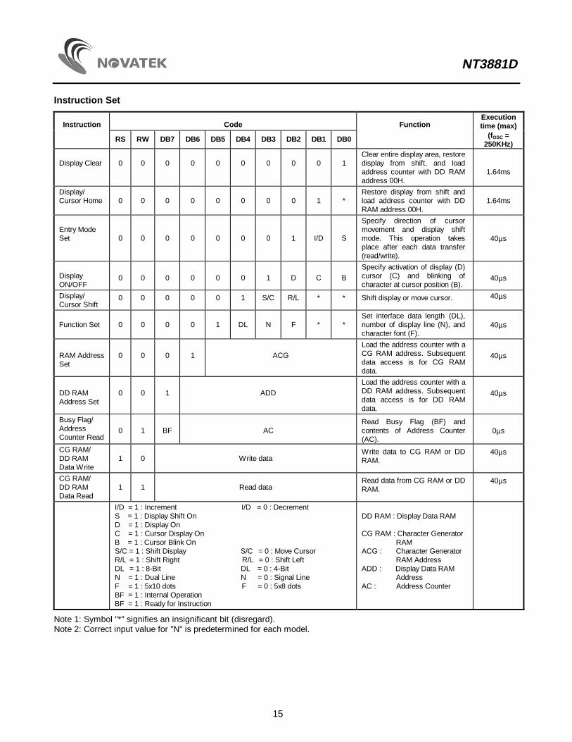
Instruction Set
Instruction Code FunctionExecutiontime (max)
RS RW DB7 DB6 DB5 DB4 DB3 DB2 DB1 DB0 (fOSC =250KHz)
Display Clear 0 0 0 0 0 0 0 0 0 1Clear entire display area, restoredisplay from shift, and loadaddress counter with DD RAMaddress 00H.
1.64ms
Display/Cursor Home 0 0 0 0 0 0 0 0 1 *
Restore display from shift andload address counter with DDRAM address 00H.
1.64ms
Entry ModeSet 0 0 0 0 0 0 0 1 I/D S
Specify direction of cursormovement and display shiftmode. This operation takesplace after each data transfer(read/write).
40µs
DisplayON/OFF
0 0 0 0 0 0 1 D C B
Specify activation of display (D)cursor (C) and blinking ofcharacter at cursor position (B).
40µs
Display/Cursor Shift
0 0 0 0 0 1 S/C R/L * * Shift display or move cursor. 40µs
Function Set 0 0 0 0 1 DL N F * *Set interface data length (DL),number of display line (N), andcharacter font (F).
40µs
RAM AddressSet
0 0 0 1 ACG
Load the address counter with aCG RAM address. Subsequentdata access is for CG RAMdata.
40µs
DD RAMAddress Set
0 0 1 ADD
Load the address counter with aDD RAM address. Subsequentdata access is for DD RAMdata.
40µs
Busy Flag/AddressCounter Read
0 1 BF ACRead Busy Flag (BF) andcontents of Address Counter(AC).
0µs
CG RAM/DD RAMData Write
1 0 Write dataWrite data to CG RAM or DDRAM.
40µs
CG RAM/DD RAMData Read
1 1 Read dataRead data from CG RAM or DDRAM.
40µs
I/D = 1 : Increment I/D = 0 : DecrementS = 1 : Display Shift OnD = 1 : Display OnC = 1 : Cursor Display OnB = 1 : Cursor Blink OnS/C = 1 : Shift Display S/C = 0 : Move CursorR/L = 1 : Shift Right R/L = 0 : Shift LeftDL = 1 : 8-Bit DL = 0 : 4-BitN = 1 : Dual Line N = 0 : Signal LineF = 1 : 5x10 dots F = 0 : 5x8 dotsBF = 1 : Internal OperationBF = 1 : Ready for Instruction
DD RAM : Display Data RAM
CG RAM : Character Generator RAMACG : Character Generator RAM AddressADD : Display Data RAM AddressAC : Address Counter
Note 1: Symbol "*" signifies an insignificant bit (disregard).Note 2: Correct input value for "N" is predetermined for each model.
NT3881D
16
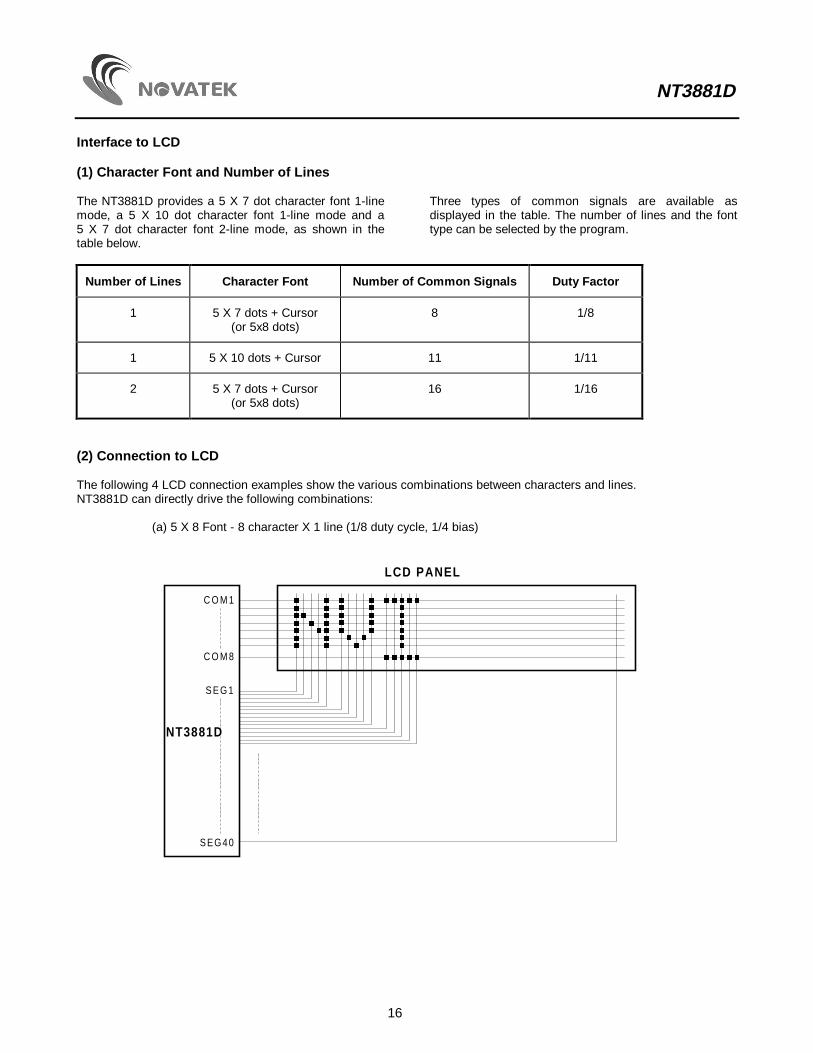
Interface to LCD
(1) Character Font and Number of Lines
The NT3881D provides a 5 X 7 dot character font 1-linemode, a 5 X 10 dot character font 1-line mode and a5 X 7 dot character font 2-line mode, as shown in thetable below.
Three types of common signals are available asdisplayed in the table. The number of lines and the fonttype can be selected by the program.
Number of Lines Character Font Number of Common Signals Duty Factor
1 5 X 7 dots + Cursor(or 5x8 dots)
8 1/8
1 5 X 10 dots + Cursor 11 1/11
2 5 X 7 dots + Cursor(or 5x8 dots)
16 1/16
(2) Connection to LCD
The following 4 LCD connection examples show the various combinations between characters and lines.NT3881D can directly drive the following combinations:
(a) 5 X 8 Font - 8 character X 1 line (1/8 duty cycle, 1/4 bias)
NT3881D
C O M 1
C O M 8
S E G 1
S E G 4 0
LCD PANEL
NT3881D
17
(b) 5 X 10 Font - 8 character X 1 line (1/11 duty cycle, 1/4 bias)
NT3881D
C O M 1
C O M 8
S E G 1
S E G 4 0
LCD PANEL
C O M 1 1
C O M 9
(c) 5 X 8 Font - 8 character X 2 lines (1/16 duty cycle, 1/5 bias)
NT3881D
COM1
COM8
SEG1
SEG40
LCD PANEL
COM16
COM9
NT3881D
18
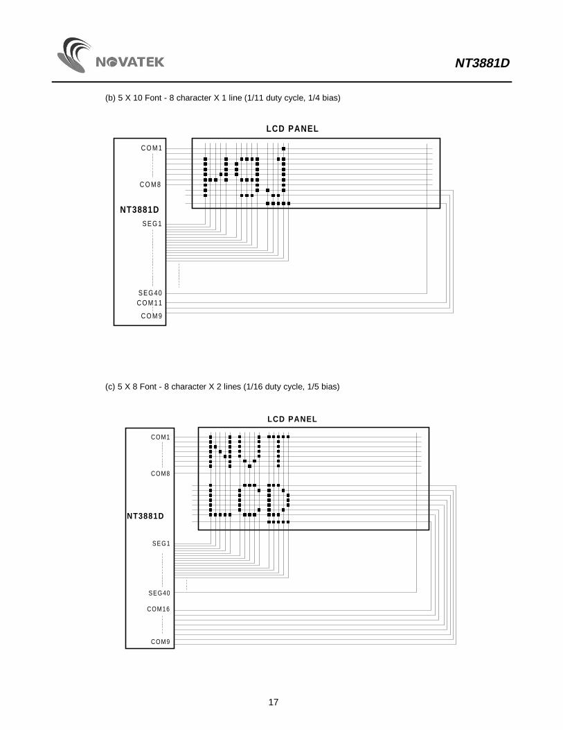
(d) 5 X 8 Font - 16 character X 1 line (1/16 duty cycle, 1/5 bias)
NT3881D
C O M 1
C O M 8
S E G 1
S E G 4 0
LCD PANEL
C O M 1 6
C O M 9
NT3881D
19
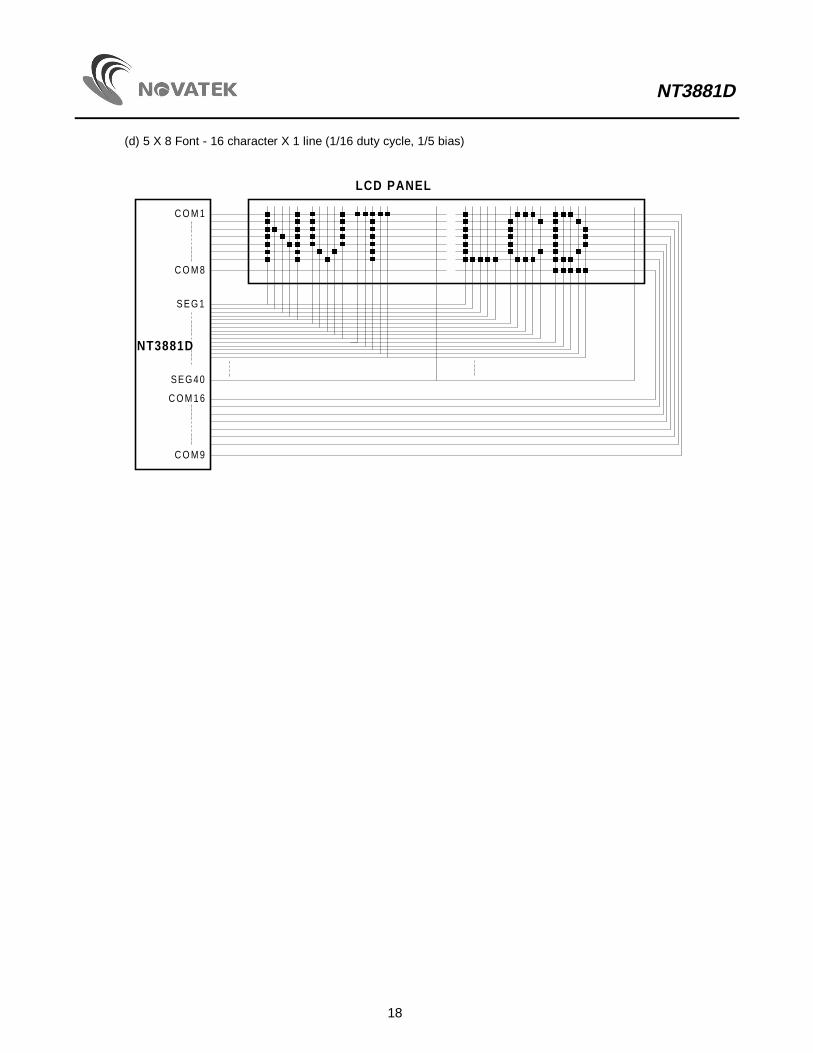
(3) Bias Power Connection
NT3881D provides 1/4 or 1/5 bias for various duty cycle applications. The power division voltage is described in thefollowing table. The connection of NT3881D, power supply, and resistors are also shown as follows:
Power Division 1/8, 1/11 Duty Cycle - 1/4 Bias 1/16 Duty Cycle - 1/5 Bias
V1 VDD - 1/4 VLCD VDD - 1/5 VLCD
V2 VDD - 1/2 VLCD VDD - 2/5 VLCD
V3 VDD - 1/2 VLCD VDD - 3/5 VLCD
V4 VDD - 3/4 VLCD VDD - 4/5 VLCD
V5 VDD - VLCD VDD - VLCD
NT3881D
V D D
V 1
V 2
V 3
V 4
V 5
V R
V E E
V D D
R
R
R
R
V LCD
V D D
V 1
V 2
V 3
V 4
V 5
V R
V D D
R
R
R
R
R
V LCD
V E E
NT3881D
Note: The resistance value depends on the LCD panel size.
NT3881D
20
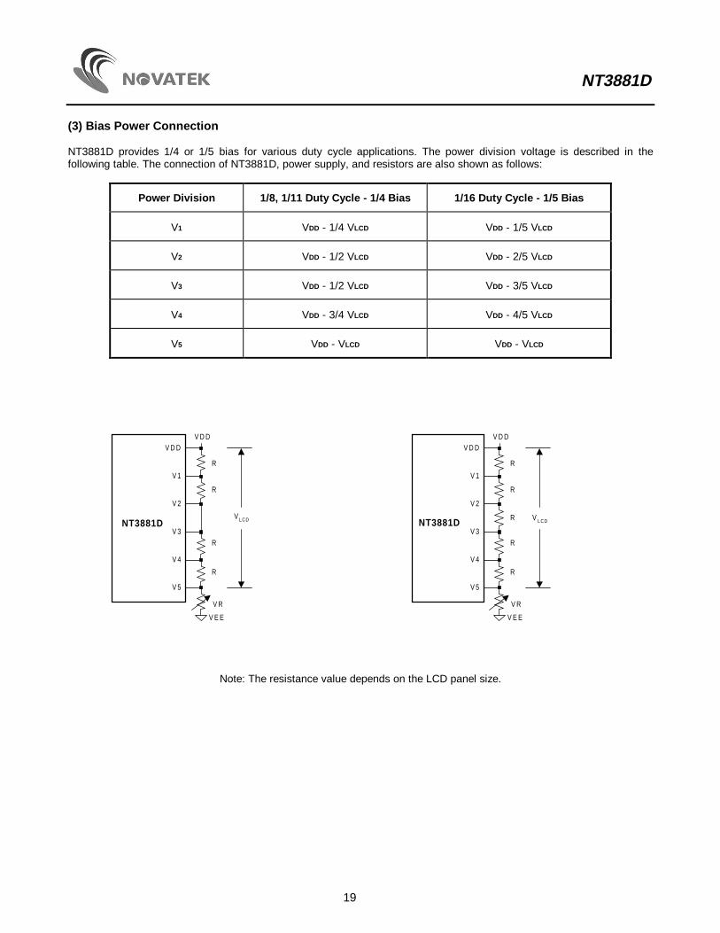
(4) LCD Waveform
A-type, 1/8 Duty Cycle, 1/4 Bias
A-type, 1/11 Duty Cycle, 1/4 Bias
A-type, 1/16 Duty Cycle, 1/5 Bias
NT3881D
21
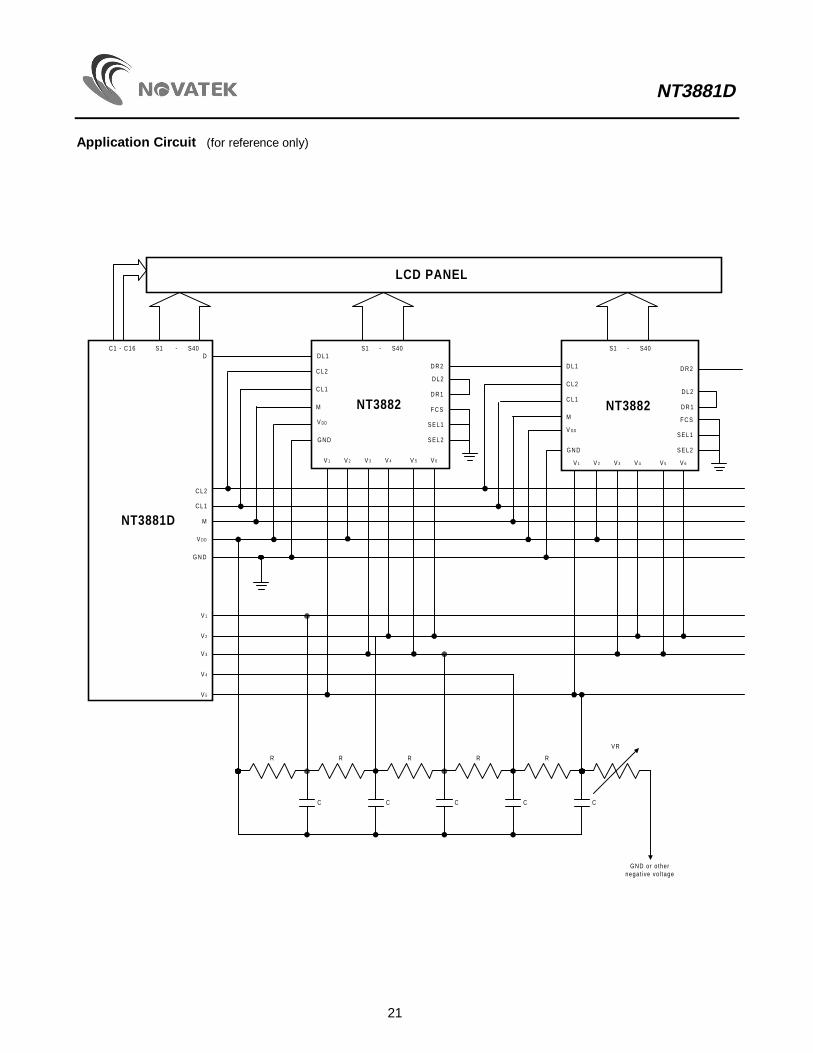
Application Circuit (for reference only)
NT3881D
LCD PANEL
NT3882
C1 - C16 S1 - S40D
C L 2
C L 1
M
V DD
G N D
V 1
V 2
V 3
V 4
V 5
D L 1
C L 2
C L 1
M
V DD
G N D
V 3 V 4 V 5
D R 1
D L 2
D R 2
S1 - S40 S1 - S40
D R 2
D L 2
D R 1
G N D
V DD
M
C L 1
C L 2
D L 1
R R R R R
VR
C C C C C
GND or o thernegat ive vo l tage
S E L 1
F C S
S E L 2
F C S
S E L 1
S E L 2
V 2 V 6V 1 V 3 V 4 V 5V 2 V 6V 1
NT3882
NT3881D
22
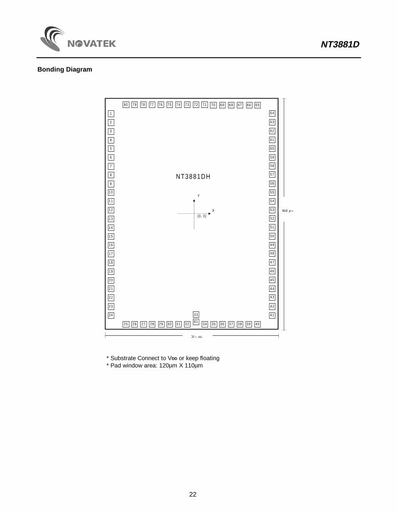
Bonding Diagram
1
2
3
4
5
6
7
8
9
1 0
1 1
1 2
1 3
1 4
1 5
1 6
1 7
1 8
1 9
2 0
2 1
2 2
2 3
2 4
2 5 2 6 2 7 2 8 2 9 3 0 3 1 3 28 1
3 4 3 5 3 6 3 7 3 8 3 9 4 0
4 1
4 2
4 3
4 4
4 5
4 6
4 7
4 8
4 9
5 0
5 1
5 2
5 3
5 4
5 5
5 6
5 7
5 8
5 9
6 0
6 1
6 2
6 3
6 4
6 56 76 86 97 07 17 27 37 47 57 67 77 87 98 0
(0, 0)
NT3881DH
Y
X
ÆÄÊÈ µ
ÆËÉÄ µ
6 6
3 3
* Substrate Connect to VDD or keep floating* Pad window area: 120µm X 110µm
NT3881D
23
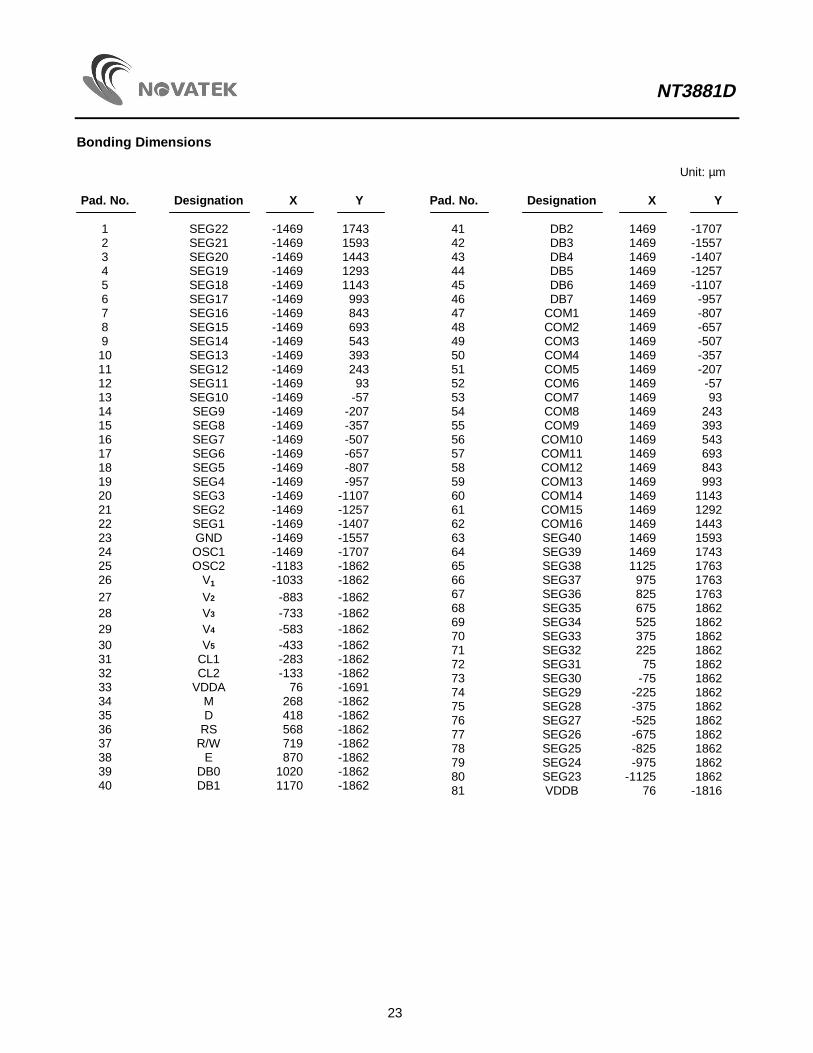
Bonding Dimensions
Unit: µm
Pad. No. Designation X Y
1 SEG22 -1469 17432 SEG21 -1469 15933 SEG20 -1469 14434 SEG19 -1469 12935 SEG18 -1469 11436 SEG17 -1469 9937 SEG16 -1469 8438 SEG15 -1469 6939 SEG14 -1469 54310 SEG13 -1469 39311 SEG12 -1469 24312 SEG11 -1469 9313 SEG10 -1469 -5714 SEG9 -1469 -20715 SEG8 -1469 -35716 SEG7 -1469 -50717 SEG6 -1469 -65718 SEG5 -1469 -80719 SEG4 -1469 -95720 SEG3 -1469 -110721 SEG2 -1469 -125722 SEG1 -1469 -140723 GND -1469 -155724 OSC1 -1469 -170725 OSC2 -1183 -186226 V1 -1033 -186227 V2 -883 -186228 V3 -733 -186229 V4 -583 -186230 V5 -433 -186231 CL1 -283 -186232 CL2 -133 -186233 VDDA 76 -169134 M 268 -186235 D 418 -186236 RS 568 -186237 R/W 719 -186238 E 870 -186239 DB0 1020 -186240 DB1 1170 -1862
Pad. No. Designation X Y
41 DB2 1469 -170742 DB3 1469 -155743 DB4 1469 -140744 DB5 1469 -125745 DB6 1469 -110746 DB7 1469 -95747 COM1 1469 -80748 COM2 1469 -65749 COM3 1469 -50750 COM4 1469 -35751 COM5 1469 -20752 COM6 1469 -5753 COM7 1469 9354 COM8 1469 24355 COM9 1469 39356 COM10 1469 54357 COM11 1469 69358 COM12 1469 84359 COM13 1469 99360 COM14 1469 114361 COM15 1469 129262 COM16 1469 144363 SEG40 1469 159364 SEG39 1469 174365 SEG38 1125 176366 SEG37 975 176367 SEG36 825 176368 SEG35 675 186269 SEG34 525 186270 SEG33 375 186271 SEG32 225 186272 SEG31 75 186273 SEG30 -75 186274 SEG29 -225 186275 SEG28 -375 186276 SEG27 -525 186277 SEG26 -675 186278 SEG25 -825 186279 SEG24 -975 186280 SEG23 -1125 186281 VDDB 76 -1816
NT3881D
24
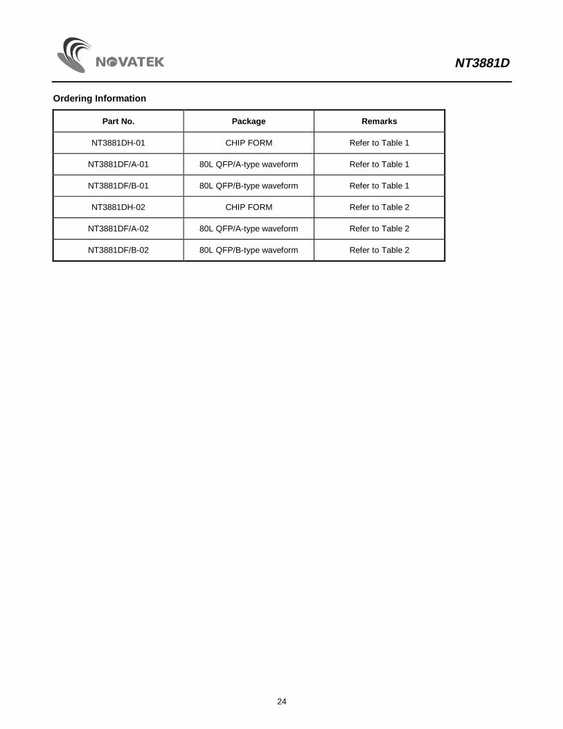
Ordering Information
Part No. Package Remarks
NT3881DH-01 CHIP FORM Refer to Table 1
NT3881DF/A-01 80L QFP/A-type waveform Refer to Table 1
NT3881DF/B-01 80L QFP/B-type waveform Refer to Table 1
NT3881DH-02 CHIP FORM Refer to Table 2
NT3881DF/A-02 80L QFP/A-type waveform Refer to Table 2
NT3881DF/B-02 80L QFP/B-type waveform Refer to Table 2
NT3881D
25
Package Information
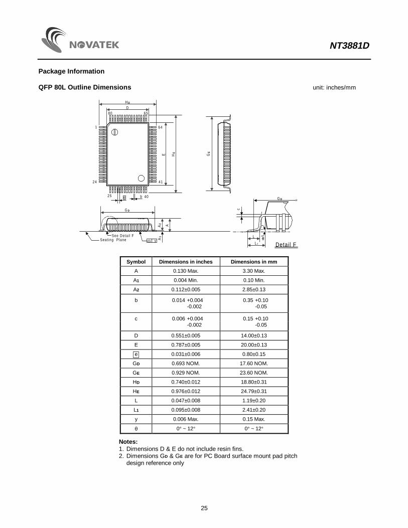
QFP 80L Outline Dimensions unit: inches/mm
A1
A2 A
Sea t ing P lane
1
2 4
b2 5 4 0
4 1
6 4
6 58 0
E
e
GE
G D
See Deta i l F
Detail F
DH D
HE
D yL
G D ~ ~~
L 1
c
Symbol Dimensions in inches Dimensions in mm
A 0.130 Max. 3.30 Max.
A1 0.004 Min. 0.10 Min.
A2 0.112±0.005 2.85±0.13
b 0.014 +0.004 0.35 +0.10-0.002 -0.05
c 0.006 +0.004 0.15 +0.10-0.002 -0.05
D 0.551±0.005 14.00±0.13
E 0.787±0.005 20.00±0.13
e 0.031±0.006 0.80±0.15
GD 0.693 NOM. 17.60 NOM.
GE 0.929 NOM. 23.60 NOM.
HD 0.740±0.012 18.80±0.31
HE 0.976±0.012 24.79±0.31
L 0.047±0.008 1.19±0.20
L1 0.095±0.008 2.41±0.20
y 0.006 Max. 0.15 Max.
θ 0° ~ 12° 0° ~ 12°
Notes:1. Dimensions D & E do not include resin fins.2. Dimensions GD & GE are for PC Board surface mount pad pitch
design reference only