Standard LCD Segment Driver - Rohmrohmfs.rohm.com/.../ic/driver/lcd_segment/bu9796axxx-e.pdfStandard...
31
○Product structure:Silicon monolithic integrated circuit ○This product is not designed protection against radioactive rays. 1/28 TSZ02201-0A2A0D300100-1-2 13.Jun.2014 Rev.003 www.rohm.com © 2013 ROHM Co., Ltd. All rights reserved. TSZ22111・14・001 Datasheet Standard LCD Segment Driver BU9796Axxx Series MAX 80 segments (SEG20×COM4) ●Features Integrated RAM for display data (DDRAM): 20 x 4 bit (Max 80 Segment) LCD drive output : 4 Common output, Max 20 Segment output Integrated Buffer AMP for LCD driving Integrated Oscillator circuit No external components Low power consumption design ●Applications Telephone FAX Portable equipment (POS, ECR, PDA etc.) DSC DVC Car audio Home electrical appliance Meter equipment etc. ●Key Specifications ■ Supply Voltage Range: +2.5V to +5.5V ■ Operating Temperature Range: -40°C to +85°C ■ Max Segments: BU9796AFS 80 Segments BU9796AMUV 48 Segments Display Duty: 1/4 ■ Bias: 1/2, 1/3 selectable ■ Interface: 2wire serial interface ●Package W (Typ.) x D (Typ.) x H (Max.) ●Typical Application Circuit Using internal oscillator Figure 1. Typical application circuit SSOP-A32 13.60mm x 7.80mm x 2.01mm VQFN024V4040 4.00mm x 4.00mm x 1.00mm Controller VDD VLCD SDA SCL OSCIN TEST1 TEST2 VSS COM0 COM1 COM2 COM3 SEG0 SEG1 Segment LCD VDD SEG19 ・・・・・・・ ・・・・・・・ BU9796AFS
Transcript of Standard LCD Segment Driver - Rohmrohmfs.rohm.com/.../ic/driver/lcd_segment/bu9796axxx-e.pdfStandard...
Product structure:Silicon monolithic integrated circuit This product is not designed protection against radioactive rays.
1/28 TSZ02201-0A2A0D300100-1-213.Jun.2014 Rev.003
www.rohm.com © 2013 ROHM Co., Ltd. All rights reserved. TSZ22111・14・001
Datasheet
Standard LCD Segment Driver BU9796Axxx Series MAX 80 segments (SEG20×COM4)
Features
Integrated RAM for display data (DDRAM): 20 x 4 bit (Max 80 Segment)
LCD drive output : 4 Common output, Max 20 Segment output
Integrated Buffer AMP for LCD driving Integrated Oscillator circuit No external components Low power consumption design
Applications
Telephone FAX Portable equipment (POS, ECR, PDA etc.) DSC DVC Car audio Home electrical appliance Meter equipment
etc.
Key Specifications
Supply Voltage Range: +2.5V to +5.5V Operating Temperature Range: -40°C to +85°C Max Segments:
BU9796AFS 80 Segments BU9796AMUV 48 Segments
Display Duty: 1/4 Bias: 1/2, 1/3 selectable Interface: 2wire serial interface
Package W (Typ.) x D (Typ.) x H (Max.)
Typical Application Circuit
Using internal oscillator
Figure 1. Typical application circuit
SSOP-A32 13.60mm x 7.80mm x 2.01mm
VQFN024V4040 4.00mm x 4.00mm x 1.00mm
Controller
VDDVLCD
SDASCL
OSCINTEST1TEST2VSS
COM0COM1COM2COM3
SEG0SEG1
SegmentLCD
VDD
SEG19
・・・
・・・
・
・・・
・・・・
BU9796AFS
2/28
BU9796Axxx Series MAX 80 segments (SEG20×COM4) Datasheet
TSZ02201-0A2A0D300100-1-213.Jun.2014 Rev.003
www.rohm.com © 2013 ROHM Co., Ltd. All rights reserved. TSZ22111・15・001
Block Diagram / Pin Configuration / Pin Description
BU9796AFS Figure 2. Block Diagram Figure 3. Pin Configuration (TOP VIEW)
Table 1 Pin Description
Terminal Terminal No. I/O Function
TEST1 26 I Test input (ROHM use only) Must be connect to VSS
TEST2 27 I
Test input (ROHM use only)TEST2=”L”: POR circuit enable TEST2=”H”: POR circuit disenable, refer to “Cautions in Power ON/OFF”
OSCIN 28 I External clock inputExternal clock and Internal clock can be selected by command. Must be connect to VSS when use internal oscillation circuit.
SDA 30 I/O serial data in-out terminal
SCL 29 I serial data transfer clock
VSS 25 GND
VDD 24 Power supply
VLCD 23 Power supply for LCD driving
SEG0-19 31,32 1-18 O SEGMENT output for LCD driving
COM0-3 19-22 O COMMON output for LCD driving
LCDBIAS
SELECTOR
Common driver
Segment driver
OSCILLATOR Power On Reset
SDA SCL
VLCD
OSCIN
VSS
COM0……COM3 SEG0…… SEG19
IF FILTER
Serial interface
Commandregister
Common counter DDRAM
LCD voltage generator
Command Data Decoder
Blink timing generator
+
-
+
-
VDD
SE
G 1
SE
G0
SD
A
SC
L
OSC
IN
TES
T 2
TES
T 1
VS
S
VD
D
VLC
D
CO
M 3
CO
M 2
CO
M 1
CO
M 0
SE
G 1
9
SE
G 1
8
SE
G 2
SE
G 3
SE
G 4
SE
G 5
SE
G 6
SE
G 7
SE
G 8
SE
G 9
SE
G 1
0
SE
G 1
1
SE
G 1
2
SE
G 1
3
SE
G 1
4
SE
G 1
5
SE
G 1
6
SE
G 1
7
3/28
BU9796Axxx Series MAX 80 segments (SEG20×COM4) Datasheet
TSZ02201-0A2A0D300100-1-213.Jun.2014 Rev.003
www.rohm.com © 2013 ROHM Co., Ltd. All rights reserved. TSZ22111・15・001
Block Diagram / Pin Configuration / Pin Description- continued
BU9796AMUV Figure 4. Block Diagram Figure 5. Pin Configuration (BOTTOM VIEW)
Table 1 Pin Description
Terminal Terminal No. I/O Function
TEST1 23 I Test input (ROHM use only) Must be connect to VSS
TEST2 24 I
Test input (ROHM use only)TEST2=”L”: POR circuit enable TEST2=”H”: POR circuit disenable, refer to “Cautions in Power ON/OFF”
OSCIN 1 I External clock inputExternal clock and Internal clock can be selected by command. Must be connect to VSS when use internal oscillation circuit.
SDA 3 I/O serial data in-out terminal
SCL 2 I serial data transfer clock
VSS 22 GND
VDD 21 Power supply
VLCD 20 Power supply for LCD driving
SEG0-11 4-15 O SEGMENT output for LCD driving
COM0-3 16-19 O COMMON output for LCD driving
EXT-PAD -(*1) - Substrate
*1: To radiate heat, please contact a board with the EXT-PAD which is located at the bottom side of VQFN024V4044 package.
Please supply VSS level or Open state as the input condition for this PAD.
LCDBIAS
SELECTOR
Common driver
Segmentdriver
OSCILLATOR Power On Reset
SDA SCL
VLCD
OSCIN
VSS
COM 0 ……COM3 SEG0…… SEG11
IF FILTER
Serial interface
Commandregister
Common counter DDRAM
LCD voltage generator
CommandData Decoder
Blink timinggenerator
+ -
+ -
VDD
OS
CIN
SC
L
SD
ASE
G0
SEG
1SE
G2
TEST2 SEG3
TEST1 SEG4
VSS SEG5
VDD SEG6
VLCD SEG7
COM3 SEG8
CO
M2
CO
M1
CO
M0
SEG
11
SEG
10SE
G9
1 2 3 4 5 6
18
17
16
15
14
13
24
23
22
21
20
19
7
8
9
10
11
12
EXT-PAD
4/28
BU9796Axxx Series MAX 80 segments (SEG20×COM4) Datasheet
TSZ02201-0A2A0D300100-1-213.Jun.2014 Rev.003
www.rohm.com © 2013 ROHM Co., Ltd. All rights reserved. TSZ22111・15・001
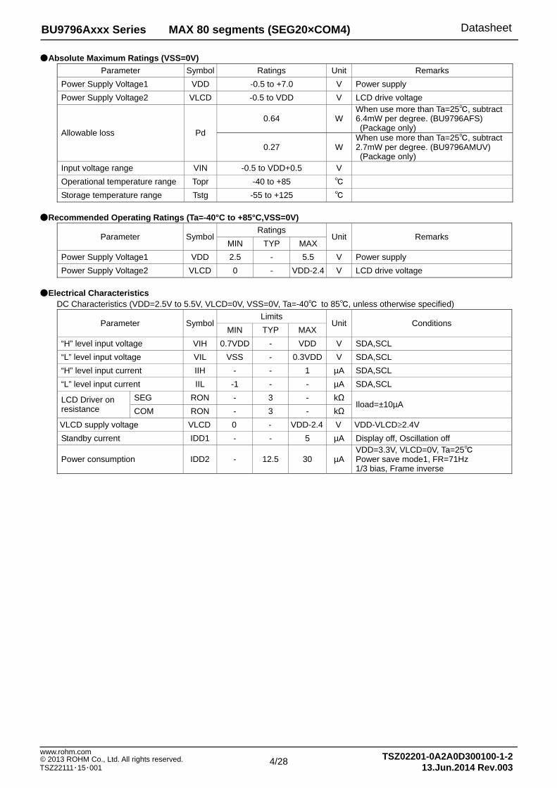
Absolute Maximum Ratings (VSS=0V) Parameter Symbol Ratings Unit Remarks
Power Supply Voltage1 VDD -0.5 to +7.0 V Power supply Power Supply Voltage2 VLCD -0.5 to VDD V LCD drive voltage
Allowable loss Pd
0.64 W When use more than Ta=25, subtract6.4mW per degree. (BU9796AFS) (Package only)
0.27 W When use more than Ta=25, subtract2.7mW per degree. (BU9796AMUV) (Package only)
Input voltage range VIN -0.5 to VDD+0.5 V Operational temperature range Topr -40 to +85 Storage temperature range Tstg -55 to +125
Recommended Operating Ratings (Ta=-40°C to +85°C,VSS=0V)
Parameter Symbol Ratings
Unit Remarks MIN TYP MAX
Power Supply Voltage1 VDD 2.5 - 5.5 V Power supply Power Supply Voltage2 VLCD 0 - VDD-2.4 V LCD drive voltage
Electrical Characteristics
DC Characteristics (VDD=2.5V to 5.5V, VLCD=0V, VSS=0V, Ta=-40 to 85, unless otherwise specified)
Parameter Symbol Limits
Unit Conditions MIN TYP MAX
“H” level input voltage VIH 0.7VDD - VDD V SDA,SCL “L” level input voltage VIL VSS - 0.3VDD V SDA,SCL “H” level input current IIH - - 1 µA SDA,SCL “L” level input current IIL -1 - - µA SDA,SCL
LCD Driver on resistance
SEG RON - 3 - kΩIload=±10µA
COM RON - 3 - kΩVLCD supply voltage VLCD 0 - VDD-2.4 V VDD-VLCD≥2.4V Standby current IDD1 - - 5 µA Display off, Oscillation off
Power consumption IDD2 - 12.5 30 µAVDD=3.3V, VLCD=0V, Ta=25Power save mode1, FR=71Hz 1/3 bias, Frame inverse
5/28
BU9796Axxx Series MAX 80 segments (SEG20×COM4) Datasheet
TSZ02201-0A2A0D300100-1-213.Jun.2014 Rev.003
www.rohm.com © 2013 ROHM Co., Ltd. All rights reserved. TSZ22111・15・001
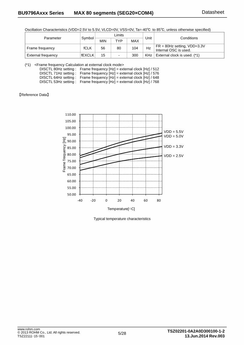
Oscillation Characteristics (VDD=2.5V to 5.5V, VLCD=0V, VSS=0V, Ta=-40 to 85, unless otherwise specified)
Parameter Symbol Limits
Unit Conditions MIN TYP MAX
Frame frequency fCLK 56 80 104 Hz FR = 80Hz setting, VDD=3.3VInternal OSC is used.
External frequency fEXCLK 15 - 300 KHz External clock is used. (*1) (*1) <Frame frequency Calculation at external clock mode>
DISCTL 80Hz setting : Frame frequency [Hz] = external clock [Hz] / 512 DISCTL 71Hz setting : Frame frequency [Hz] = external clock [Hz] / 576 DISCTL 64Hz setting : Frame frequency [Hz] = external clock [Hz] / 648 DISCTL 53Hz setting : Frame frequency [Hz] = external clock [Hz] / 768
【Reference Data】
Typical temperature characteristics
50.00
55.00
60.00
65.00
70.00
75.00
80.00
85.00
90.00
95.00
100.00
105.00
110.00
‐40 ‐20 0 20 40 60 80
Fram
e fr
eque
ncy
[Hz]
Temperature[C]
VDD = 2.5V
VDD = 3.3V
VDD = 5.0V VDD = 5.5V
6/28
BU9796Axxx Series MAX 80 segments (SEG20×COM4) Datasheet
TSZ02201-0A2A0D300100-1-213.Jun.2014 Rev.003
www.rohm.com © 2013 ROHM Co., Ltd. All rights reserved. TSZ22111・15・001
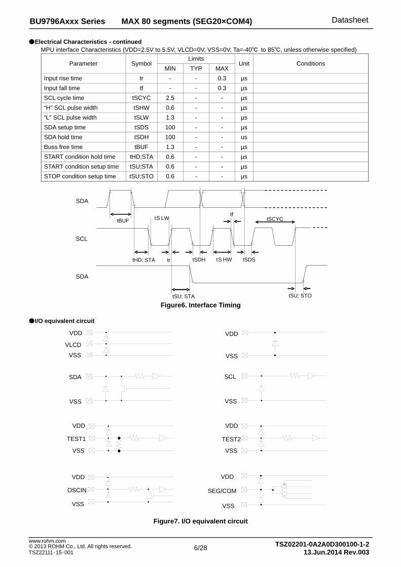
Electrical Characteristics - continued MPU interface Characteristics (VDD=2.5V to 5.5V, VLCD=0V, VSS=0V, Ta=-40 to 85, unless otherwise specified)
Parameter Symbol Limits
Unit Conditions MIN TYP MAX
Input rise time tr - - 0.3 µs Input fall time tf - - 0.3 µs SCL cycle time tSCYC 2.5 - - µs “H” SCL pulse width tSHW 0.6 - - µs “L” SCL pulse width tSLW 1.3 - - µs SDA setup time tSDS 100 - - µs SDA hold time tSDH 100 - - us Buss free time tBUF 1.3 - - µs START condition hold time tHD;STA 0.6 - - µs START condition setup time tSU;STA 0.6 - - µs STOP condition setup time tSU;STO 0.6 - - µs
Figure6. Interface Timing
I/O equivalent circuit
Figure7. I/O equivalent circuit
tBUF
SDA
SCL
tSDH
SDA
tHD; STA
tS LW
tr tS HW
tf
tSDS
tSU; STA tSU; STO
tSCYC
VDD
VLCD
VSS
VDD
TEST1
VSS
VDD
SEG/COM
VSS
SDA
VSS
VDD
VSS
SCL
VSS
VDD
TEST2
VSS
VDD
OSCIN
VSS
7/28
BU9796Axxx Series MAX 80 segments (SEG20×COM4) Datasheet
TSZ02201-0A2A0D300100-1-213.Jun.2014 Rev.003
www.rohm.com © 2013 ROHM Co., Ltd. All rights reserved. TSZ22111・15・001
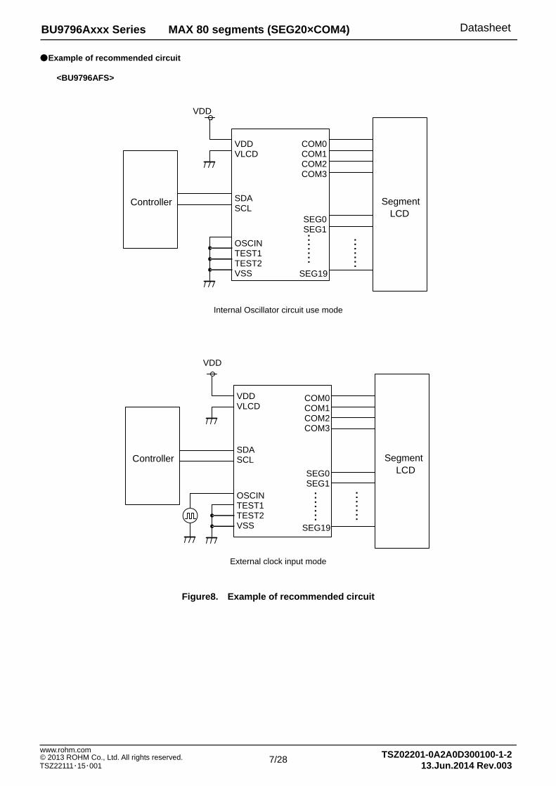
Example of recommended circuit
<BU9796AFS>
Internal Oscillator circuit use mode
External clock input mode
Figure8. Example of recommended circuit
Controller
VDDVLCD
SDASCL
OSCINTEST1TEST2VSS
COM0COM1COM2COM3
SEG0SEG1
SegmentLCD
VDD
SEG19
・・・
・・・
・
・・・
・・・・
Controller
VDDVLCD
SDASCL
OSCINTEST1TEST2VSS
COM0COM1COM2COM3
SEG0SEG1
SegmentLCD
VDD
SEG19
・・・・・
・・
・・・・・
・・
8/28
BU9796Axxx Series MAX 80 segments (SEG20×COM4) Datasheet
TSZ02201-0A2A0D300100-1-213.Jun.2014 Rev.003
www.rohm.com © 2013 ROHM Co., Ltd. All rights reserved. TSZ22111・15・001
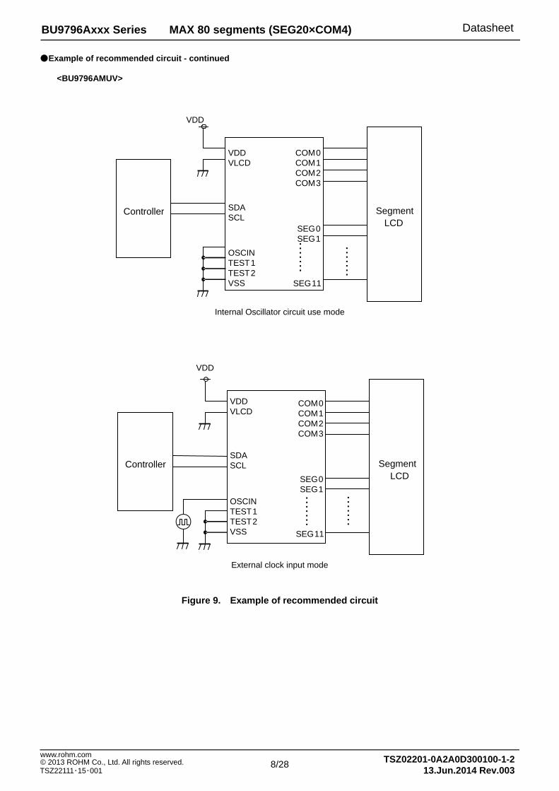
Example of recommended circuit - continued
<BU9796AMUV>
Internal Oscillator circuit use mode
External clock input mode
Figure 9. Example of recommended circuit
Controller
VDDVLCD
SDASCL
OSCINTEST1TEST2VSS
COM0COM1COM2COM3
SEG0SEG1
Segment LCD
VDD
SEG11・・・・・・・
・・・・・・・
Controller
VDDVLCD
SDASCL
OSCINTEST1TEST2VSS
COM0COM1COM2COM3
SEG0SEG1
SegmentLCD
VDD
SEG11・・・・・・・
・・・・・・・
9/28
BU9796Axxx Series MAX 80 segments (SEG20×COM4) Datasheet
TSZ02201-0A2A0D300100-1-213.Jun.2014 Rev.003
www.rohm.com © 2013 ROHM Co., Ltd. All rights reserved. TSZ22111・15・001
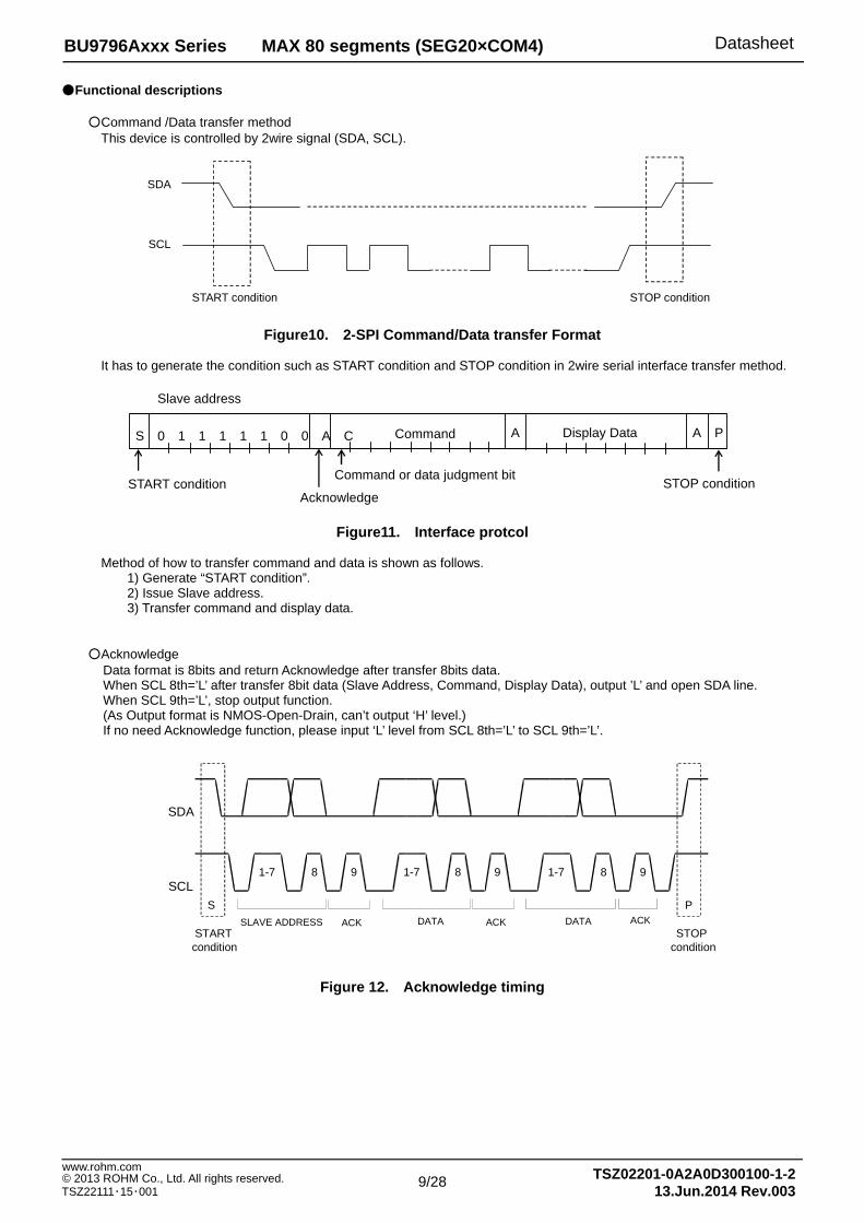
Functional descriptions
Command /Data transfer method This device is controlled by 2wire signal (SDA, SCL).
Figure10. 2-SPI Command/Data transfer Format
It has to generate the condition such as START condition and STOP condition in 2wire serial interface transfer method.
Figure11. Interface protcol
Method of how to transfer command and data is shown as follows. 1) Generate “START condition”. 2) Issue Slave address. 3) Transfer command and display data.
Acknowledge Data format is 8bits and return Acknowledge after transfer 8bits data. When SCL 8th=’L’ after transfer 8bit data (Slave Address, Command, Display Data), output ’L’ and open SDA line. When SCL 9th=’L’, stop output function. (As Output format is NMOS-Open-Drain, can’t output ‘H’ level.) If no need Acknowledge function, please input ‘L’ level from SCL 8th=’L’ to SCL 9th=’L’.
Figure 12. Acknowledge timing
START condition STOP condition
SDA
SCL
Slave address
S 0 1 1 1 1 1 0 0 A C
0
Command Display Data A A P
AcknowledgeSTART condition
Command or data judgment bit STOP condition
SDA
SCL1-7 8 9 1-7 8 9 1-7 8 9
SLAVE ADDRESS ACK DATA ACK DATA ACKS P
STARTcondition
STOPcondition
10/28
BU9796Axxx Series MAX 80 segments (SEG20×COM4) Datasheet
TSZ02201-0A2A0D300100-1-213.Jun.2014 Rev.003
www.rohm.com © 2013 ROHM Co., Ltd. All rights reserved. TSZ22111・15・001
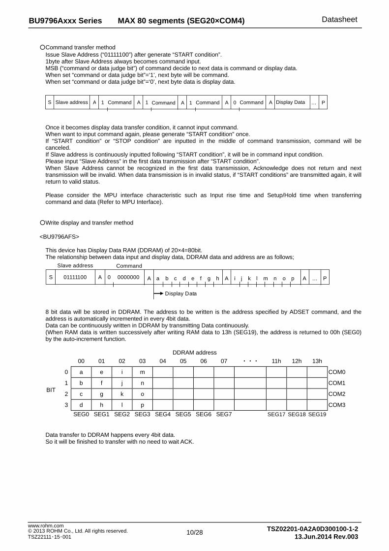
Command transfer method
Issue Slave Address (“01111100”) after generate “START condition”. 1byte after Slave Address always becomes command input. MSB (“command or data judge bit”) of command decide to next data is command or display data. When set “command or data judge bit”=‘1’, next byte will be command. When set “command or data judge bit”=‘0’, next byte data is display data.
Slave address A 1 S Command A 1 Command A 1 Command A 0 Command A … PDisplay Data
Once it becomes display data transfer condition, it cannot input command. When want to input command again, please generate “START condition” once. If “START condition” or “STOP condition” are inputted in the middle of command transmission, command will be canceled. If Slave address is continuously inputted following “START condition”, it will be in command input condition. Please input “Slave Address” in the first data transmission after “START condition”. When Slave Address cannot be recognized in the first data transmission, Acknowledge does not return and next transmission will be invalid. When data transmission is in invalid status, if “START conditions” are transmitted again, it will return to valid status. Please consider the MPU interface characteristic such as Input rise time and Setup/Hold time when transferring command and data (Refer to MPU Interface).
Write display and transfer method <BU9796AFS>
This device has Display Data RAM (DDRAM) of 20×4=80bit. The relationship between data input and display data, DDRAM data and address are as follows;
01111100 A 0 S 0000000 A a b c d e f g h A i j k l m n o p A … P
Display Data
Slave address Command
8 bit data will be stored in DDRAM. The address to be written is the address specified by ADSET command, and the address is automatically incremented in every 4bit data. Data can be continuously written in DDRAM by transmitting Data continuously. (When RAM data is written successively after writing RAM data to 13h (SEG19), the address is returned to 00h (SEG0) by the auto-increment function.
DDRAM address 00 01 02 03 04 05 06 07 ・・・ 11h 12h 13h
BIT
0 a e i m COM0
1 b f j n COM1
2 c g k o COM2
3 d h l p COM3 SEG0 SEG1 SEG2 SEG3 SEG4 SEG5 SEG6 SEG7 SEG17 SEG18 SEG19
Data transfer to DDRAM happens every 4bit data. So it will be finished to transfer with no need to wait ACK.
11/28
BU9796Axxx Series MAX 80 segments (SEG20×COM4) Datasheet
TSZ02201-0A2A0D300100-1-213.Jun.2014 Rev.003
www.rohm.com © 2013 ROHM Co., Ltd. All rights reserved. TSZ22111・15・001
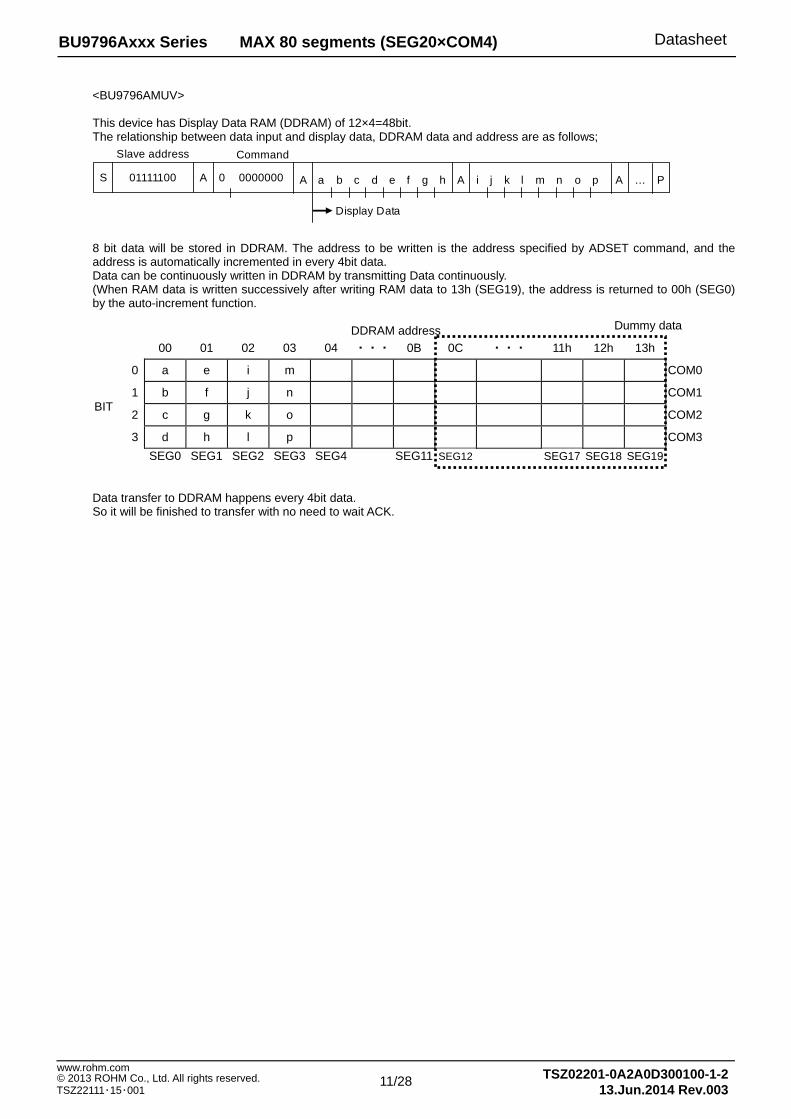
<BU9796AMUV> This device has Display Data RAM (DDRAM) of 12×4=48bit. The relationship between data input and display data, DDRAM data and address are as follows;
01111100 A 0 S 0000000 A a b c d e f g h A i j k l m n o p A … P
Display Data
Slave address Command
8 bit data will be stored in DDRAM. The address to be written is the address specified by ADSET command, and the address is automatically incremented in every 4bit data. Data can be continuously written in DDRAM by transmitting Data continuously. (When RAM data is written successively after writing RAM data to 13h (SEG19), the address is returned to 00h (SEG0) by the auto-increment function.
DDRAM address 00 01 02 03 04 ・・・ 0B 0C ・・・ 11h 12h 13h
BIT
0 a e i m COM0
1 b f j n COM1
2 c g k o COM2
3 d h l p COM3 SEG0 SEG1 SEG2 SEG3 SEG4 SEG11 SEG12 SEG17 SEG18 SEG19
Data transfer to DDRAM happens every 4bit data. So it will be finished to transfer with no need to wait ACK.
Dummy data
12/28
BU9796Axxx Series MAX 80 segments (SEG20×COM4) Datasheet
TSZ02201-0A2A0D300100-1-213.Jun.2014 Rev.003
www.rohm.com © 2013 ROHM Co., Ltd. All rights reserved. TSZ22111・15・001
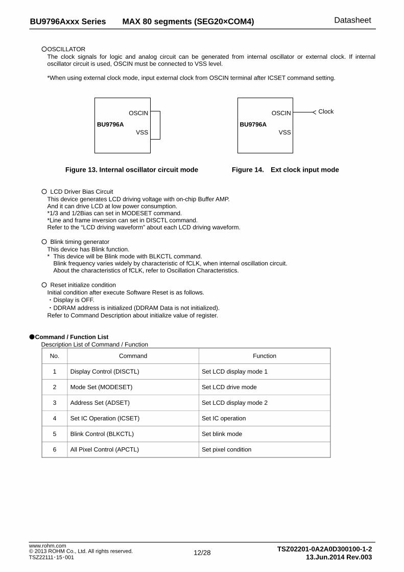
OSCILLATOR
The clock signals for logic and analog circuit can be generated from internal oscillator or external clock. If internal oscillator circuit is used, OSCIN must be connected to VSS level. *When using external clock mode, input external clock from OSCIN terminal after ICSET command setting.
Figure 13. Internal oscillator circuit mode Figure 14. Ext clock input mode
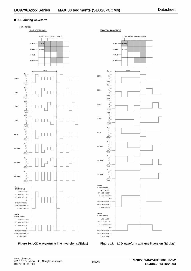
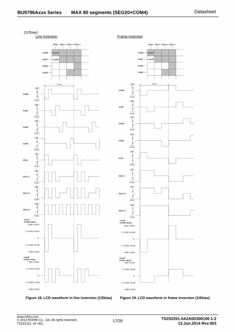
LCD Driver Bias Circuit This device generates LCD driving voltage with on-chip Buffer AMP. And it can drive LCD at low power consumption. *1/3 and 1/2Bias can set in MODESET command. *Line and frame inversion can set in DISCTL command. Refer to the “LCD driving waveform” about each LCD driving waveform.
Blink timing generator This device has Blink function. * This device will be Blink mode with BLKCTL command. Blink frequency varies widely by characteristic of fCLK, when internal oscillation circuit. About the characteristics of fCLK, refer to Oscillation Characteristics.
Reset initialize condition Initial condition after execute Software Reset is as follows. ・Display is OFF. ・DDRAM address is initialized (DDRAM Data is not initialized). Refer to Command Description about initialize value of register.
Command / Function List
Description List of Command / Function
No. Command Function
1 Display Control (DISCTL) Set LCD display mode 1
2 Mode Set (MODESET) Set LCD drive mode
3 Address Set (ADSET) Set LCD display mode 2
4 Set IC Operation (ICSET) Set IC operation
5 Blink Control (BLKCTL) Set blink mode
6 All Pixel Control (APCTL) Set pixel condition
OSCIN
BU9796A VSS
OSCIN
BU9796A VSS
Clock
13/28
BU9796Axxx Series MAX 80 segments (SEG20×COM4) Datasheet
TSZ02201-0A2A0D300100-1-213.Jun.2014 Rev.003
www.rohm.com © 2013 ROHM Co., Ltd. All rights reserved. TSZ22111・15・001
Detailed command description
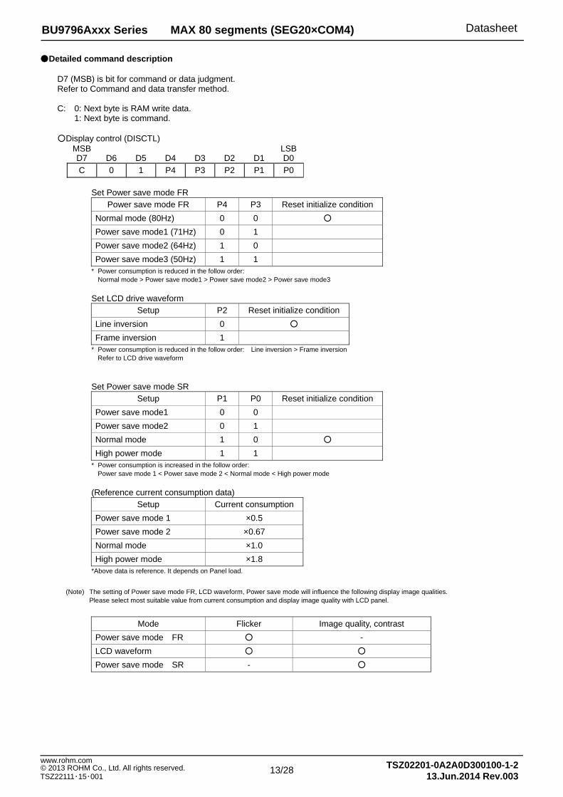
D7 (MSB) is bit for command or data judgment. Refer to Command and data transfer method. C: 0: Next byte is RAM write data. 1: Next byte is command. Display control (DISCTL)
MSB D7
D6
D5 D4
D3
D2 D1
LSB D0
C 0 1 P4 P3 P2 P1 P0 Set Power save mode FR
Power save mode FR P4 P3 Reset initialize condition Normal mode (80Hz) 0 0 Power save mode1 (71Hz) 0 1 Power save mode2 (64Hz) 1 0 Power save mode3 (50Hz) 1 1
* Power consumption is reduced in the follow order: Normal mode > Power save mode1 > Power save mode2 > Power save mode3 Set LCD drive waveform
Setup P2 Reset initialize condition Line inversion 0 Frame inversion 1
* Power consumption is reduced in the follow order: Line inversion > Frame inversion Refer to LCD drive waveform Set Power save mode SR
Setup P1 P0 Reset initialize condition Power save mode1 0 0 Power save mode2 0 1 Normal mode 1 0 High power mode 1 1
* Power consumption is increased in the follow order: Power save mode 1 < Power save mode 2 < Normal mode < High power mode (Reference current consumption data)
Setup Current consumption Power save mode 1 ×0.5 Power save mode 2 ×0.67 Normal mode ×1.0 High power mode ×1.8
*Above data is reference. It depends on Panel load.
(Note) The setting of Power save mode FR, LCD waveform, Power save mode will influence the following display image qualities. Please select most suitable value from current consumption and display image quality with LCD panel.
Mode Flicker Image quality, contrast
Power save mode FR - LCD waveform Power save mode SR -
14/28
BU9796Axxx Series MAX 80 segments (SEG20×COM4) Datasheet
TSZ02201-0A2A0D300100-1-213.Jun.2014 Rev.003
www.rohm.com © 2013 ROHM Co., Ltd. All rights reserved. TSZ22111・15・001
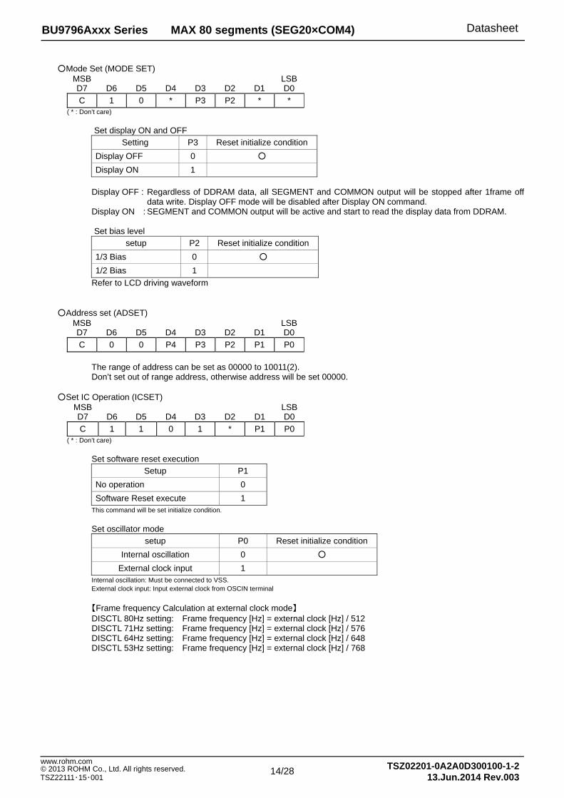
Mode Set (MODE SET)
MSB D7
D6
D5 D4
D3
D2 D1
LSB D0
C 1 0 * P3 P2 * * ( * : Don’t care)
Set display ON and OFF
Setting P3 Reset initialize condition Display OFF 0 Display ON 1
Display OFF : Regardless of DDRAM data, all SEGMENT and COMMON output will be stopped after 1frame off
data write. Display OFF mode will be disabled after Display ON command. Display ON : SEGMENT and COMMON output will be active and start to read the display data from DDRAM. Set bias level
setup P2 Reset initialize condition 1/3 Bias 0 1/2 Bias 1
Refer to LCD driving waveform
Address set (ADSET) MSB D7
D6
D5 D4
D3
D2 D1
LSB D0
C 0 0 P4 P3 P2 P1 P0 The range of address can be set as 00000 to 10011(2). Don’t set out of range address, otherwise address will be set 00000.
Set IC Operation (ICSET) MSB D7
D6
D5 D4
D3
D2 D1
LSB D0
C 1 1 0 1 * P1 P0 ( * : Don’t care)
Set software reset execution
Setup P1 No operation 0 Software Reset execute 1
This command will be set initialize condition. Set oscillator mode
setup P0 Reset initialize condition Internal oscillation 0
External clock input 1 Internal oscillation: Must be connected to VSS. External clock input: Input external clock from OSCIN terminal 【Frame frequency Calculation at external clock mode】 DISCTL 80Hz setting: Frame frequency [Hz] = external clock [Hz] / 512 DISCTL 71Hz setting: Frame frequency [Hz] = external clock [Hz] / 576 DISCTL 64Hz setting: Frame frequency [Hz] = external clock [Hz] / 648 DISCTL 53Hz setting: Frame frequency [Hz] = external clock [Hz] / 768
15/28
BU9796Axxx Series MAX 80 segments (SEG20×COM4) Datasheet
TSZ02201-0A2A0D300100-1-213.Jun.2014 Rev.003
www.rohm.com © 2013 ROHM Co., Ltd. All rights reserved. TSZ22111・15・001
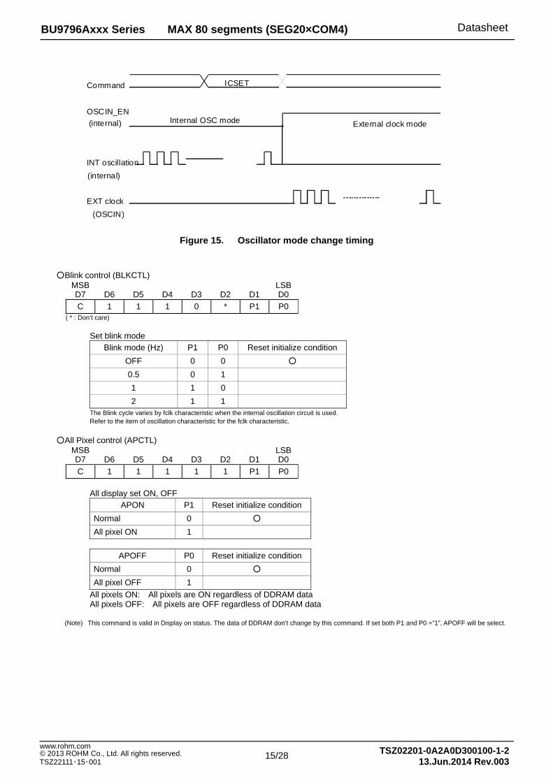
Command ICSET
OSCIN_EN(internal) Internal OSC mode External clock mode
INT oscillation (internal)
EXT clock(OSCIN)
Figure 15. Oscillator mode change timing
Blink control (BLKCTL) MSB D7
D6
D5 D4
D3
D2 D1
LSB D0
C 1 1 1 0 * P1 P0 ( * : Don’t care)
Set blink mode
Blink mode (Hz) P1 P0 Reset initialize condition OFF 0 0 0.5 0 1 1 1 0 2 1 1
The Blink cycle varies by fclk characteristic when the internal oscillation circuit is used. Refer to the item of oscillation characteristic for the fclk characteristic.
All Pixel control (APCTL)
MSB D7
D6
D5 D4
D3
D2 D1
LSB D0
C 1 1 1 1 1 P1 P0 All display set ON, OFF
APON P1 Reset initialize condition Normal 0 All pixel ON 1
APOFF P0 Reset initialize condition
Normal 0 All pixel OFF 1
All pixels ON: All pixels are ON regardless of DDRAM data All pixels OFF: All pixels are OFF regardless of DDRAM data
(Note) This command is valid in Display on status. The data of DDRAM don’t change by this command. If set both P1 and P0 =”1”, APOFF will be select.
16/28
BU9796Axxx Series MAX 80 segments (SEG20×COM4) Datasheet
TSZ02201-0A2A0D300100-1-213.Jun.2014 Rev.003
www.rohm.com © 2013 ROHM Co., Ltd. All rights reserved. TSZ22111・15・001
LCD driving waveform
(1/3bias) Line inversion Frame inversion
Figure 16. LCD waveform at line inversion (1/3bias) Figure 17. LCD waveform at frame inversion (1/3bias)
1frame
COM0
COM1
COM2
COM3
SEGn
SEGn+1
SEGn+2
SEGn+3
SEGn+2 SEGn+3
COM3
stateA
SEGn SEGn+1
COM0
COM1
COM2
stateB
VDD
VLCD
VDD
VLCD
VDD
VLCD
VDD
VLCD
VDD
VLCD
VDD
VLCD
VDD
VLCD
VDD
VLCD
(VDD-VLCD)
2/3 (VDD-VLCD)
1/3 (VDD-VLCD)
-1/3 (VDD-VLCD)
-2/3 (VDD-VLCD)
- (VDD-VLCD)
stateA
(COM0-SEGn)
0
stateB
(COM1-SEGn)
(VDD-VLCD)
2/3 (VDD-VLCD)
1/3 (VDD-VLCD)
-1/3 (VDD-VLCD)
-2/3 (VDD-VLCD)
- (VDD-VLCD)
0
1frame
COM0
COM1
COM2
COM3
SEGn
SEGn+1
SEGn+2
SEGn+3
COM2
COM3
COM0 stateA
COM1 stateB
SEGn SEGn+1 SEGn+2 SEGn+3
VDD
VLCD
VDD
VLCD
VDD
VLCD
VDD
VLCD
VDD
VLCD
VDD
VLCD
VDD
VLCD
VDD
VLCD
(VDD-VLCD)
2/3 (VDD-VLCD)
1/3 (VDD-VLCD)
-1/3 (VDD-VLCD)
-2/3 (VDD-VLCD)
- (VDD-VLCD)
stateA
(COM0-SEGn)
0
stateB
(COM1-SEGn)
(VDD-VLCD)
2/3 (VDD-VLCD)
1/3 (VDD-VLCD)
-1/3 (VDD-VLCD)
-2/3 (VDD-VLCD)
-(VDD-VLCD)
0
17/28
BU9796Axxx Series MAX 80 segments (SEG20×COM4) Datasheet
TSZ02201-0A2A0D300100-1-213.Jun.2014 Rev.003
www.rohm.com © 2013 ROHM Co., Ltd. All rights reserved. TSZ22111・15・001
(1/2bias) Line inversion Frame inversion
Figure 18. LCD waveform in line inversion (1/2bias) Figure 19. LCD waveform in frame inversion (1/2bias)
1frame
COM0
COM1
COM2
COM3
SEGn
SEGn+1
SEGn+2
SEGn+3
SEGn SEGn+1 SEGn+2 SEGn+3
COM0 stateA
COM1 stateB
COM2
COM3
VDD
VLCD
VDD
VLCD
VDD
VLCD
VDD
VLCD
VDD
VLCD
VDD
VLCD
VDD
VLCD
VDD
VLCD
stateB
(COM1-SEGn)
stateA
(COM0-SEGn)
(VDD-VLCD)
1/2 (VDD-VLCD)
-1/2 (VDD-VLCD)
-(VDD-VLCD)
0
(VDD-VLCD)
1/2 (VDD-VLCD)
-1/2 (VDD-VLCD)
-(VDD-VLCD)
0
1frame
COM0
COM1
COM2
COM3
SEGn
SEGn+1
SEGn+2
SEGn+3
SEGn SEGn+1
COM2
COM3
SEGn+2 SEGn+3
COM0 stateA
COM1 stateB
VDD
VLCD
VDD
VLCD
VDD
VLCD
VDD
VLCD
VDD
VLCD
VDD
VLCD
VDD
VLCD
VDD
VLCD
(VDD-VLCD)
1/2 (VDD-VLCD)
-1/2 (VDD-VLCD)
-(VDD-VLCD)
0
stateA
(COM0-SEGn)
stateB
(COM1-SEGn)(VDD-VLCD)
1/2 (VDD-VLCD)
-1/2 (VDD-VLCD)
-(VDD-VLCD)
0
18/28
BU9796Axxx Series MAX 80 segments (SEG20×COM4) Datasheet
TSZ02201-0A2A0D300100-1-213.Jun.2014 Rev.003
www.rohm.com © 2013 ROHM Co., Ltd. All rights reserved. TSZ22111・15・001
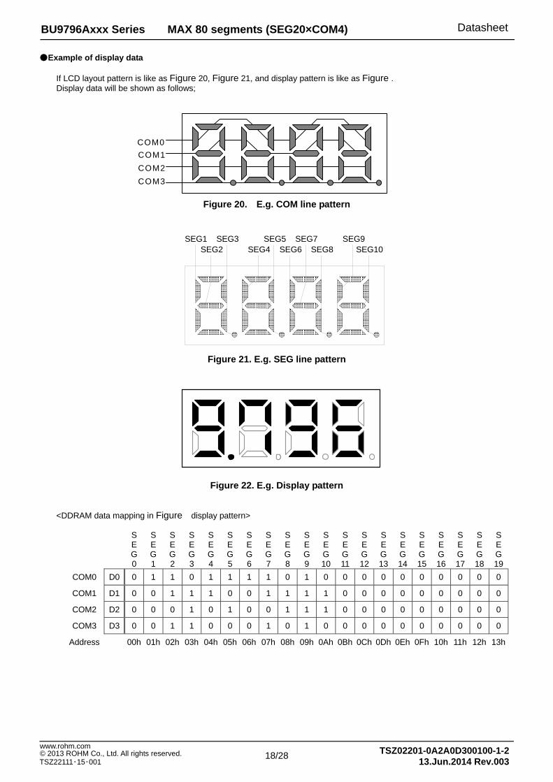
Example of display data If LCD layout pattern is like as Figure 20, Figure 21, and display pattern is like as Figure . Display data will be shown as follows;
Figure 20. E.g. COM line pattern
Figure 21. E.g. SEG line pattern
Figure 22. E.g. Display pattern
<DDRAM data mapping in Figure display pattern>
S E G 0
S E G 1
S E G 2
S E G 3
S E G 4
SEG5
SEG6
SEG7
SEG8
SEG9
SEG10
SEG11
SEG12
SEG13
S E G 14
S E G 15
S E G 16
SEG17
SEG18
SEG19
COM0 D0 0 1 1 0 1 1 1 1 0 1 0 0 0 0 0 0 0 0 0 0
COM1 D1 0 0 1 1 1 0 0 1 1 1 1 0 0 0 0 0 0 0 0 0
COM2 D2 0 0 0 1 0 1 0 0 1 1 1 0 0 0 0 0 0 0 0 0
COM3 D3 0 0 1 1 0 0 0 1 0 1 0 0 0 0 0 0 0 0 0 0
Address 00h 01h 02h 03h 04h 05h 06h 07h 08h 09h 0Ah 0Bh 0Ch 0Dh 0Eh 0Fh 10h 11h 12h 13h
SEG1 SEG2
SEG3SEG4
SEG5SEG6
SEG7SEG8
SEG9SEG10
COM1COM2COM3
COM0
19/28
BU9796Axxx Series MAX 80 segments (SEG20×COM4) Datasheet
TSZ02201-0A2A0D300100-1-213.Jun.2014 Rev.003
www.rohm.com © 2013 ROHM Co., Ltd. All rights reserved. TSZ22111・15・001
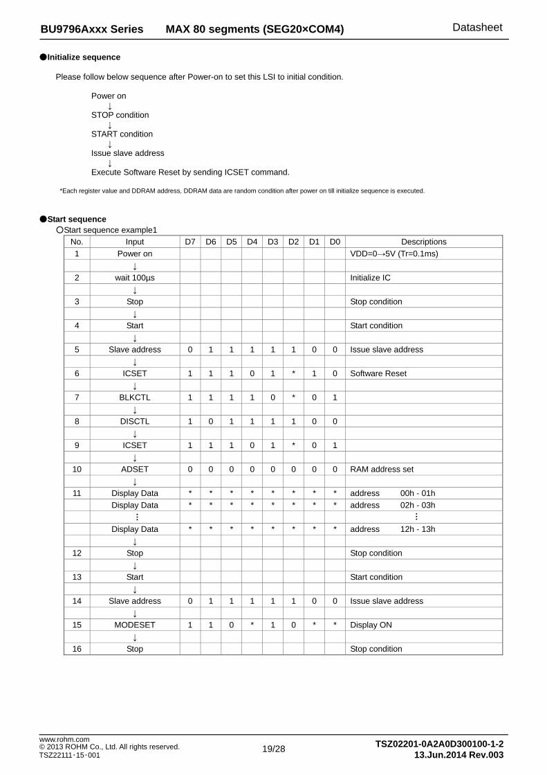
Initialize sequence Please follow below sequence after Power-on to set this LSI to initial condition.
Power on ↓ STOP condition ↓ START condition ↓ Issue slave address ↓ Execute Software Reset by sending ICSET command.
*Each register value and DDRAM address, DDRAM data are random condition after power on till initialize sequence is executed.
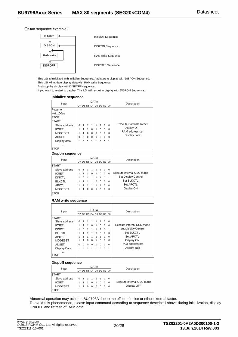
Start sequence
Start sequence example1 No. Input D7 D6 D5 D4 D3 D2 D1 D0 Descriptions 1 Power on VDD=0→5V (Tr=0.1ms) ↓ 2 wait 100µs Initialize IC ↓ 3 Stop Stop condition ↓ 4 Start Start condition ↓ 5 Slave address 0 1 1 1 1 1 0 0 Issue slave address ↓ 6 ICSET 1 1 1 0 1 * 1 0 Software Reset ↓ 7 BLKCTL 1 1 1 1 0 * 0 1 ↓ 8 DISCTL 1 0 1 1 1 1 0 0 ↓ 9 ICSET 1 1 1 0 1 * 0 1 ↓
10 ADSET 0 0 0 0 0 0 0 0 RAM address set ↓
11 Display Data * * * * * * * * address 00h - 01h Display Data * * * * * * * * address 02h - 03h …
…
Display Data * * * * * * * * address 12h - 13h ↓
12 Stop Stop condition ↓
13 Start Start condition ↓
14 Slave address 0 1 1 1 1 1 0 0 Issue slave address ↓
15 MODESET 1 1 0 * 1 0 * * Display ON ↓
16 Stop Stop condition
20/28
BU9796Axxx Series MAX 80 segments (SEG20×COM4) Datasheet
TSZ02201-0A2A0D300100-1-213.Jun.2014 Rev.003
www.rohm.com © 2013 ROHM Co., Ltd. All rights reserved. TSZ22111・15・001
Start sequence example2
Abnormal operation may occur in BU9796A due to the effect of noise or other external factor. To avoid this phenomenon, please input command according to sequence described above during initialization, display
ON/OFF and refresh of RAM data.
Initialize sequence
D7 D6 D5 D4 D3 D2 D1 D0
Slave address 0 1 1 1 1 1 0 0
ICSET 1 1 1 0 1 0 1 0
MODESET 1 1 0 0 0 0 0 0
ADSET 0 0 0 0 0 0 0 0
Display data * * * * * * * *
Dispon sequence
D7 D6 D5 D4 D3 D2 D1 D0
Slave address 0 1 1 1 1 1 0 0
ICSET 1 1 1 0 1 0 0 0
DISCTL 1 0 1 1 1 1 1 1
BLKCTL 1 1 1 1 0 0 0 0
APCTL 1 1 1 1 1 1 0 0MODESET 1 1 0 0 1 0 0 0
RAM write sequence
D7 D6 D5 D4 D3 D2 D1 D0
Slave address 0 1 1 1 1 1 0 0
ICSET 1 1 1 0 1 0 0 0
DISCTL 1 0 1 1 1 1 1 1
BLKCTL 1 1 1 1 0 0 0 0
APCTLMODESETADSET 0 0 0 0 0 0 0 0
Display Data * * * * * * * *
Dispoff sequence
D7 D6 D5 D4 D3 D2 D1 D0
Slave address 0 1 1 1 1 1 0 0
ICSET 1 1 1 0 1 0 0 0
MODESET 1 1 0 0 0 0 0 0
InputDATA
Description
Power onwait 100usSTOPSTART
…STOP
InputDATA
Description
START
STOP
Input DATA Description
START
…STOP
STOP
InputDATA
Description
START
Initialize Sequence
DISPON Sequence
RAM write Sequence
DISPOFF Sequence
This LSI is initialized with Initialize Sequence. And start to display with DISPON Sequence.This LSI will update display data with RAM write Sequence. And stop the display with DISPOFF sequence.If you want to restart to display, This LSI will restart to display with DISPON Sequence.
Initialize
RAM write
DISPOFF
DISPON
Execute Software ResetDisplay OFF
RAM address setDisplay data
Execute internal OSC modeSet Display Control
Set BLKCTLSet APCTLDisplay ON
Execute internal OSC modeSet Display Control
Set BLKCTLSet APCTLDisplay ON
RAM address setDisplay data
Execute internal OSC modeDisplay OFF
1 1 1 1 1 1 0 01 1 0 0 1 0 0 0

21/28
BU9796Axxx Series MAX 80 segments (SEG20×COM4) Datasheet
TSZ02201-0A2A0D300100-1-213.Jun.2014 Rev.003
www.rohm.com © 2013 ROHM Co., Ltd. All rights reserved. TSZ22111・15・001
DISCTL setup flow chart
START
Power save FR = Normal Mode Line inversionPower save SR = High Power Mode
Power consumption
PicturequalityReduce Power consumption
orBest picture image quality
Yes
Display flicker exist? No
Power save FR = Save mode3 Frame inversion Power save SR = Save mode1
DISCTL setting"10111100"
Power save FR = Save mode2 Frame inversion Power save SR = Save mode1
DISCTL setting"10110100"
Yes
Display flicker exist? No
Power save FR = Save mode1 Frame inversion Power save SR = Save mode1
DISCTL setting"10101100"
Yes
Display flicker exist? No
Power save FR = Normal Frame inversion Power save SR = Save mode1
DISCTL setting"10100100"
Power save FR = Save mode3 Frame inversionPower save SR = Save mode1
Power save FR = Save mode2 Frame inversion Power save SR = Save mode1
Power save FR = Save mode1 Line inversionPower save SR = Save mode1
DISCTL setting"10100011"
DISCTL setting"10111100"
DISCTL setting"10110100"
DISCTL setting"10101100"

22/28
BU9796Axxx Series MAX 80 segments (SEG20×COM4) Datasheet
TSZ02201-0A2A0D300100-1-213.Jun.2014 Rev.003
www.rohm.com © 2013 ROHM Co., Ltd. All rights reserved. TSZ22111・15・001
VDD tF tR
tOFF Vbot
Cautions in Power ON/OFF
This device has “P.O.R” (Power-On Reset) circuit and Software Reset function. Please keep the following recommended Power-On conditions in order to power up properly.
Please set power up conditions to meet the recommended tR, tF, tOFF, and Vbot spec below in order to ensure P.O.R operation *It has to set TEST1=”L” to be valid in POR circuit.
Recommended condition of tR, tF, tOFF, Vbot (Ta=25) tR tF tOFF Vbot
Less than 1ms
Less than 1ms
More than 100ms
Less than 0.1V
Figure 23. Power ON/OFF waveform
If it is difficult to meet above conditions, execute the following sequence after Power-On.
* It has to keep the following sequence in the case of TEST2=”H”. As POR circuit is invalid status. But it is not able to accept Command input in Power off status, it has to take care that software reset is not perfectly alternative method of POR function.
(1) Generate STOP condition
Figure 24. Stop Condition
(2) Generate START condition.
Figure 25. Start Condition (3) Issue slave address (4) Execute Software Reset (ICSET) command
23/28
BU9796Axxx Series MAX 80 segments (SEG20×COM4) Datasheet
TSZ02201-0A2A0D300100-1-213.Jun.2014 Rev.003
www.rohm.com © 2013 ROHM Co., Ltd. All rights reserved. TSZ22111・15・001
Operational Notes (1) Absolute Maximum Ratings
An excess in the absolute maximum ratings, such as supply voltage, temperature range of operating conditions, etc., can break down devices, thus making impossible to identify breaking mode such as a short circuit or an open circuit. If any special mode exceeding the absolute maximum ratings is assumed, consideration should be given to take physical safety measures including the use of fuses, etc.
(2) Operating conditions These conditions represent a range within which characteristics can be provided approximately as expected. The electrical characteristics are guaranteed under the conditions of each parameter.
(3) Reverse connection of power supply connector The reverse connection of power supply connector can break down ICs. Take protective measures against the breakdown due to the reverse connection, such as mounting an external diode between the power supply and the IC’s power supply terminal.
(4) Power supply line Design PCB pattern to provide low impedance for the wiring between the power supply and the GND lines. In this regard, or the digital block power supply and the analog block power supply, even though these power supplies has the same level of potential, separate the power supply pattern for the digital block from that for the analog block, thus suppressing the diffraction of digital noises to the analog block power supply resulting from impedance common to the wiring patterns. For the GND line, give consideration to design the patterns in a similar manner. Furthermore, for all power supply terminals to ICs, mount a capacitor between the power supply and the GND terminal. At the same time, in order to use an electrolytic capacitor, thoroughly check to be sure the characteristics of the capacitor to be used present no problem including the occurrence of capacity dropout at a low temperature, thus determining the constant.
(5) GND voltage Make setting of the potential of the GND terminal so that it will be maintained at the minimum in any operating state. Furthermore, check to be sure no terminals are at a potential lower than the GND voltage including an actual electric transient.
(6) Short circuit between terminals and erroneous mounting In order to mount ICs on a set PCB, pay thorough attention to the direction and offset of the ICs. Erroneous mounting can break down the ICs. Furthermore, if a short circuit occurs due to foreign matters entering between terminals or between the terminal and the power supply or the GND terminal, the ICs can break down.
(7) Operation in strong electromagnetic field Be noted that using ICs in the strong electromagnetic field can malfunction them.
(8) Inspection with set PCB On the inspection with the set PCB, if a capacitor is connected to a low-impedance IC terminal, the IC can suffer stress. Therefore, be sure to discharge from the set PCB by each process. Furthermore, in order to mount or dismount the set PCB to/from the jig for the inspection process, be sure to turn OFF the power supply and then mount the set PCB to the jig. After the completion of the inspection, be sure to turn OFF the power supply and then dismount it from the jig. In addition, for protection against static electricity, establish a ground for the assembly process and pay thorough attention to the transportation and the storage of the set PCB.
(9) Input terminals In terms of the construction of IC, parasitic elements are inevitably formed in relation to potential. The operation of the parasitic element can cause interference with circuit operation, thus resulting in a malfunction and then breakdown of the input terminal. Therefore, pay thorough attention not to handle the input terminals, such as to apply to the input terminals a voltage lower than the GND respectively, so that any parasitic element will operate. Furthermore, do not apply a voltage to the input terminals when no power supply voltage is applied to the IC. In addition, even if the power supply voltage is applied, apply to the input terminals a voltage lower than the power supply voltage or within the guaranteed value of electrical characteristics.
(10) Ground wiring pattern If small-signal GND and large-current GND are provided, It will be recommended to separate the large-current GND pattern from the small-signal GND pattern and establish a single ground at the reference point of the set PCB so that resistance to the wiring pattern and voltage fluctuations due to a large current will cause no fluctuations in voltages of the small-signal GND. Pay attention not to cause fluctuations in the GND wiring pattern of external parts as well.
(11) External capacitor In order to use a ceramic capacitor as the external capacitor, determine the constant with consideration given to a degradation in the nominal capacitance due to DC bias and changes in the capacitance due to temperature, etc.
(12) No Connecting input terminals In terms of extremely high impedance of CMOS gate, to open the input terminals causes unstable state. And unstable state brings the inside gate voltage of p-channel or n-channel transistor into active. As a result, battery current may increase. And unstable state can also causes unexpected operation of IC. So unless otherwise specified, input terminals not being used should be connected to the power supply or GND line.
(13) Rush current When power is first supplied to the CMOS IC, it is possible that the internal logic may be unstable and rush current may flow instantaneously. Therefore, give special condition to power coupling capacitance, power wiring, width of GND wiring, and routing of connections.
24/28
BU9796Axxx Series MAX 80 segments (SEG20×COM4) Datasheet
TSZ02201-0A2A0D300100-1-213.Jun.2014 Rev.003
www.rohm.com © 2013 ROHM Co., Ltd. All rights reserved. TSZ22111・15・001
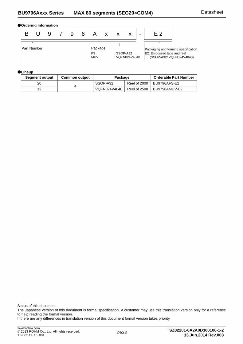
Ordering Information
B U 9 7 9 6 A x x x - E 2
Part Number Package Packaging and forming specification E2: Embossed tape and reel
(SSOP-A32/ VQFN024V4040) FS
MUV : SSOP-A32 : VQFN024V4040
Lineup Segment output Common output Package Orderable Part Number
20 4
SSOP-A32 Reel of 2000 BU9796AFS-E2 12 VQFN024V4040 Reel of 2500 BU9796AMUV-E2
Status of this document The Japanese version of this document is formal specification. A customer may use this translation version only for a reference to help reading the formal version. If there are any differences in translation version of this document formal version takes priority.
25/28
BU9796Axxx Series MAX 80 segments (SEG20×COM4) Datasheet
TSZ02201-0A2A0D300100-1-213.Jun.2014 Rev.003
www.rohm.com © 2013 ROHM Co., Ltd. All rights reserved. TSZ22111・15・001
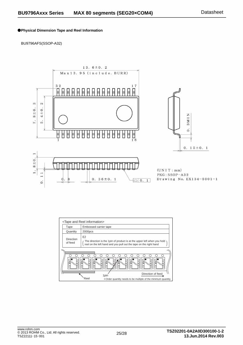
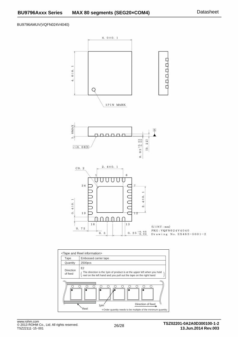
Physical Dimension Tape and Reel Information
BU9796AFS(SSOP-A32)
∗ Order quantity needs to be multiple of the minimum quantity.
<Tape and Reel information>
Embossed carrier tapeTape
Quantity
Direction of feed
The direction is the 1pin of product is at the upper left when you hold reel on the left hand and you pull out the tape on the right hand
2000pcs
E2
( )
Direction of feed
Reel1pin
26/28
BU9796Axxx Series MAX 80 segments (SEG20×COM4) Datasheet
TSZ02201-0A2A0D300100-1-213.Jun.2014 Rev.003
www.rohm.com © 2013 ROHM Co., Ltd. All rights reserved. TSZ22111・15・001
BU9796AMUV(VQFN024V4040)
∗ Order quantity needs to be multiple of the minimum quantity.
<Tape and Reel information>
Embossed carrier tapeTape
Quantity
Direction of feed
The direction is the 1pin of product is at the upper left when you hold reel on the left hand and you pull out the tape on the right hand
2500pcs
E2
( )
Direction of feed
Reel1pin
27/28
BU9796Axxx Series MAX 80 segments (SEG20×COM4) Datasheet
TSZ02201-0A2A0D300100-1-213.Jun.2014 Rev.003
www.rohm.com © 2013 ROHM Co., Ltd. All rights reserved. TSZ22111・15・001
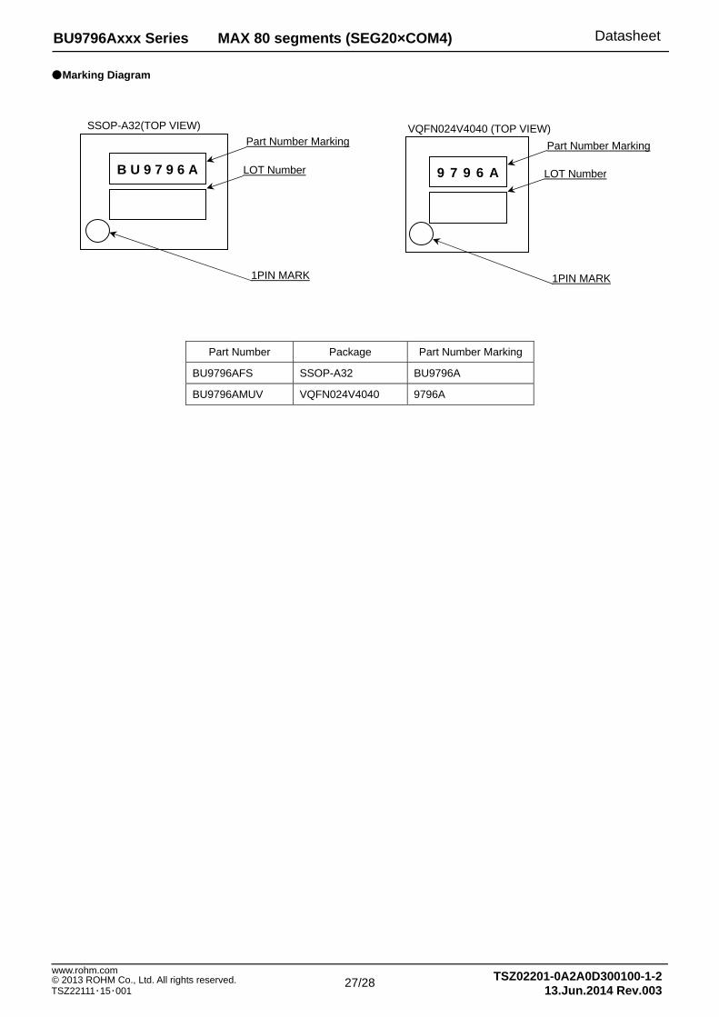
Marking Diagram
Part Number Package Part Number Marking
BU9796AFS SSOP-A32 BU9796A
BU9796AMUV VQFN024V4040 9796A
SSOP-A32(TOP VIEW)
B U 9 7 9 6 A
Part Number Marking
LOT Number
1PIN MARK
VQFN024V4040 (TOP VIEW)
9 7 9 6 A
Part Number Marking
LOT Number
1PIN MARK
28/28
BU9796Axxx Series MAX 80 segments (SEG20×COM4) Datasheet
TSZ02201-0A2A0D300100-1-213.Jun.2014 Rev.003
www.rohm.com © 2013 ROHM Co., Ltd. All rights reserved. TSZ22111・15・001
Revision History Date Revision Changes
31. Aug.2012 001 New Release 16. Jul. 2013 002 Add description for External Clock and Temperature Characteristics in page 5 13. Jun. 2014 003 Add Frame frequency Calculation at external clock mode in page 14
DatasheetDatasheet
Notice – GE Rev.002© 2013 ROHM Co., Ltd. All rights reserved.
Notice Precaution on using ROHM Products
1. Our Products are designed and manufactured for application in ordinary electronic equipments (such as AV equipment, OA equipment, telecommunication equipment, home electronic appliances, amusement equipment, etc.). If you intend to use our Products in devices requiring extremely high reliability (such as medical equipment (Note 1), transport equipment, traffic equipment, aircraft/spacecraft, nuclear power controllers, fuel controllers, car equipment including car accessories, safety devices, etc.) and whose malfunction or failure may cause loss of human life, bodily injury or serious damage to property (“Specific Applications”), please consult with the ROHM sales representative in advance. Unless otherwise agreed in writing by ROHM in advance, ROHM shall not be in any way responsible or liable for any damages, expenses or losses incurred by you or third parties arising from the use of any ROHM’s Products for Specific Applications.
(Note1) Medical Equipment Classification of the Specific Applications JAPAN USA EU CHINA
CLASSⅢ CLASSⅢ
CLASSⅡb CLASSⅢ
CLASSⅣ CLASSⅢ
2. ROHM designs and manufactures its Products subject to strict quality control system. However, semiconductor products can fail or malfunction at a certain rate. Please be sure to implement, at your own responsibilities, adequate safety measures including but not limited to fail-safe design against the physical injury, damage to any property, which a failure or malfunction of our Products may cause. The following are examples of safety measures:
[a] Installation of protection circuits or other protective devices to improve system safety [b] Installation of redundant circuits to reduce the impact of single or multiple circuit failure
3. Our Products are designed and manufactured for use under standard conditions and not under any special or extraordinary environments or conditions, as exemplified below. Accordingly, ROHM shall not be in any way responsible or liable for any damages, expenses or losses arising from the use of any ROHM’s Products under any special or extraordinary environments or conditions. If you intend to use our Products under any special or extraordinary environments or conditions (as exemplified below), your independent verification and confirmation of product performance, reliability, etc, prior to use, must be necessary:
[a] Use of our Products in any types of liquid, including water, oils, chemicals, and organic solvents [b] Use of our Products outdoors or in places where the Products are exposed to direct sunlight or dust [c] Use of our Products in places where the Products are exposed to sea wind or corrosive gases, including Cl2,
H2S, NH3, SO2, and NO2 [d] Use of our Products in places where the Products are exposed to static electricity or electromagnetic waves [e] Use of our Products in proximity to heat-producing components, plastic cords, or other flammable items [f] Sealing or coating our Products with resin or other coating materials [g] Use of our Products without cleaning residue of flux (even if you use no-clean type fluxes, cleaning residue of
flux is recommended); or Washing our Products by using water or water-soluble cleaning agents for cleaning residue after soldering
[h] Use of the Products in places subject to dew condensation
4. The Products are not subject to radiation-proof design. 5. Please verify and confirm characteristics of the final or mounted products in using the Products. 6. In particular, if a transient load (a large amount of load applied in a short period of time, such as pulse. is applied,
confirmation of performance characteristics after on-board mounting is strongly recommended. Avoid applying power exceeding normal rated power; exceeding the power rating under steady-state loading condition may negatively affect product performance and reliability.
7. De-rate Power Dissipation (Pd) depending on Ambient temperature (Ta). When used in sealed area, confirm the actual
ambient temperature. 8. Confirm that operation temperature is within the specified range described in the product specification. 9. ROHM shall not be in any way responsible or liable for failure induced under deviant condition from what is defined in
this document.
Precaution for Mounting / Circuit board design 1. When a highly active halogenous (chlorine, bromine, etc.) flux is used, the residue of flux may negatively affect product
performance and reliability. 2. In principle, the reflow soldering method must be used; if flow soldering method is preferred, please consult with the
ROHM representative in advance. For details, please refer to ROHM Mounting specification

DatasheetDatasheet
Notice – GE Rev.002© 2013 ROHM Co., Ltd. All rights reserved.
Precautions Regarding Application Examples and External Circuits 1. If change is made to the constant of an external circuit, please allow a sufficient margin considering variations of the
characteristics of the Products and external components, including transient characteristics, as well as static characteristics.
2. You agree that application notes, reference designs, and associated data and information contained in this document
are presented only as guidance for Products use. Therefore, in case you use such information, you are solely responsible for it and you must exercise your own independent verification and judgment in the use of such information contained in this document. ROHM shall not be in any way responsible or liable for any damages, expenses or losses incurred by you or third parties arising from the use of such information.
Precaution for Electrostatic
This Product is electrostatic sensitive product, which may be damaged due to electrostatic discharge. Please take proper caution in your manufacturing process and storage so that voltage exceeding the Products maximum rating will not be applied to Products. Please take special care under dry condition (e.g. Grounding of human body / equipment / solder iron, isolation from charged objects, setting of Ionizer, friction prevention and temperature / humidity control).
Precaution for Storage / Transportation 1. Product performance and soldered connections may deteriorate if the Products are stored in the places where:
[a] the Products are exposed to sea winds or corrosive gases, including Cl2, H2S, NH3, SO2, and NO2 [b] the temperature or humidity exceeds those recommended by ROHM [c] the Products are exposed to direct sunshine or condensation [d] the Products are exposed to high Electrostatic
2. Even under ROHM recommended storage condition, solderability of products out of recommended storage time period may be degraded. It is strongly recommended to confirm solderability before using Products of which storage time is exceeding the recommended storage time period.
3. Store / transport cartons in the correct direction, which is indicated on a carton with a symbol. Otherwise bent leads
may occur due to excessive stress applied when dropping of a carton. 4. Use Products within the specified time after opening a humidity barrier bag. Baking is required before using Products of
which storage time is exceeding the recommended storage time period.
Precaution for Product Label QR code printed on ROHM Products label is for ROHM’s internal use only.
Precaution for Disposition When disposing Products please dispose them properly using an authorized industry waste company.
Precaution for Foreign Exchange and Foreign Trade act Since our Products might fall under controlled goods prescribed by the applicable foreign exchange and foreign trade act, please consult with ROHM representative in case of export.
Precaution Regarding Intellectual Property Rights 1. All information and data including but not limited to application example contained in this document is for reference
only. ROHM does not warrant that foregoing information or data will not infringe any intellectual property rights or any other rights of any third party regarding such information or data. ROHM shall not be in any way responsible or liable for infringement of any intellectual property rights or other damages arising from use of such information or data.:
2. No license, expressly or implied, is granted hereby under any intellectual property rights or other rights of ROHM or any
third parties with respect to the information contained in this document.
Other Precaution 1. This document may not be reprinted or reproduced, in whole or in part, without prior written consent of ROHM. 2. The Products may not be disassembled, converted, modified, reproduced or otherwise changed without prior written
consent of ROHM. 3. In no event shall you use in any way whatsoever the Products and the related technical information contained in the
Products or this document for any military purposes, including but not limited to, the development of mass-destruction weapons.
4. The proper names of companies or products described in this document are trademarks or registered trademarks of
ROHM, its affiliated companies or third parties.

DatasheetDatasheet
Notice – WE Rev.001© 2014 ROHM Co., Ltd. All rights reserved.
General Precaution 1. Before you use our Pro ducts, you are requested to care fully read this document and fully understand its contents.
ROHM shall n ot be in an y way responsible or liabl e for fa ilure, malfunction or acci dent arising from the use of a ny ROHM’s Products against warning, caution or note contained in this document.
2. All information contained in this docume nt is current as of the issuing date and subj ect to change without any prior
notice. Before purchasing or using ROHM’s Products, please confirm the la test information with a ROHM sale s representative.
3. The information contained in this doc ument is provi ded on an “as is” basis and ROHM does not warrant that all
information contained in this document is accurate an d/or error-free. ROHM shall not be in an y way responsible or liable for any damages, expenses or losses incurred by you or third parties resulting from inaccuracy or errors of or concerning such information.