Exclusive Tutorial for MSP430 Development Board · 2.2 RGB LED ... The free version is limited to 4...
58
MSP430 Development Board (MSP-EXP430G2) This e-book contains all the necessary information for everyone that is interested in learning C programming to control variety of cool stuff and do awesome works. Suitable for beginners. Brought to you by: Embedded Project Hunter Exclusive Tutorial for
Transcript of Exclusive Tutorial for MSP430 Development Board · 2.2 RGB LED ... The free version is limited to 4...
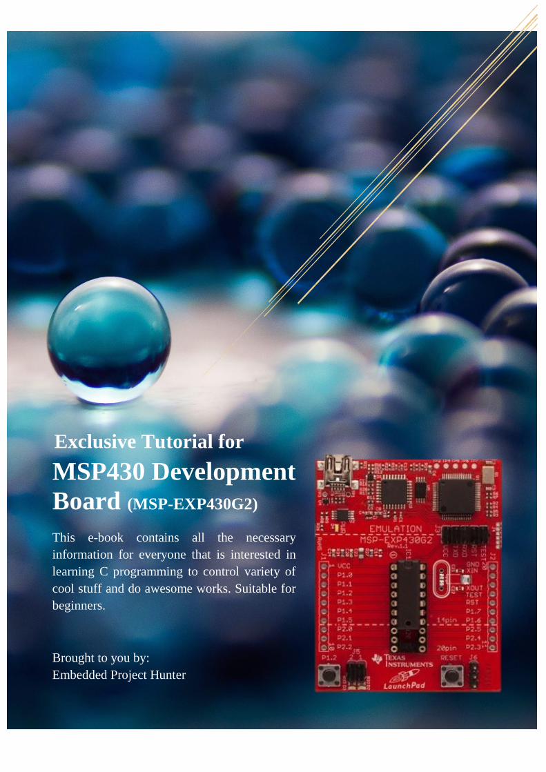
MSP430 Development
Board (MSP-EXP430G2)
This e-book contains all the necessary
information for everyone that is interested in
learning C programming to control variety of
cool stuff and do awesome works. Suitable for
beginners.
Brought to you by:
Embedded Project Hunter
Exclusive Tutorial for
For more free projects, go to www.embeddedprojecthunter.com i
Disclaimer
This e-book serves the ultimate purpose of sharing of knowledge. Efforts have
been made to ensure the errors occurred in this e-book is at its minimum level. If
you found any mistakes in this e-book, the author will appreciate it if you can
contact him through email ([email protected]) and tell him
where the mistake is so that it can be corrected and more people will be benefited.
The author shall not take any liability and responsibility for any errors in this e-
book, any losses, or damages caused directly or indirectly by this e-book.
Also, some of the codes, libraries, and images are obtained from third-party. The
codes and libraries are shared because of its practicality and usefulness. The
author will not bare any responsibility if there is any mistakes in the third-party
codes, and libraries. If you found any contents in this e-book are inappropriate
and need to be amended, please contact the author through email. He would love
to accept any kind of comments.
Knowledge are meant to be shared. Feel free to share this e-book to anyone that
suits.

For more free projects, go to www.embeddedprojecthunter.com ii
About the Author
Good day everyone!!
I am Hunter K, the author of this e-
book. Thank you for downloading
this e-book and please feel free to
email me if you have any concern
regarding this e-book.
If you never heard of MSP430 Launchpad or its microcontroller, this e-book suits
you perfectly. For more projects, you can visit my blog – Embedded Project
Hunter (EPH) blog at www.embeddedprojecthunter.com.
This book is free because I think that knowledge should be shared. Behind the
scene, I have put a lot of effort in making sure this e-book can be completed and
try to explain the codes as detail as possible. If you think that I deserve a cup of
coffee, you are more than welcome to donate by PayPal.
Feel free to share this e-book, and hope that you enjoy reading!!
Sincerely,
Hunter K.

For more free projects, go to www.embeddedprojecthunter.com iii
Download & Purchase Link
For more free projects, go to www.embeddedprojecthunter.com iv
Table of Content
Disclaimer .............................................................................................................. i
About the Author ..................................................................................................ii
Download & Purchase Link ................................................................................ iii
Table of Content ................................................................................................... iv
CHAPTER 1 - WELCOME ABOARD ................................................................ 1
1.0 Introduction ................................................................................................. 2
1.1 Start Programming ...................................................................................... 4
1.1.0 Simple LED Programming .................................................................. 7
1.1.1 Simple Button Programming ............................................................. 11
1.1.2 Button Programming with Interrupt .................................................. 14
1.2 What is Pull-Up and Pull-Down Resistor? ............................................... 16
1.3 Debounce… Bounce... Bounce… ............................................................. 17
1.4 Important Coding Syntax .......................................................................... 19
1.5 Digital Operation ...................................................................................... 21
CHAPTER 2 – INDICATORS AND DISPLAYS ............................................. 23
2.0 Introduction ............................................................................................... 24
2.1 Seven-Segment Display ............................................................................ 25
2.1.0 Simple Display One Two Three ........................................................ 26
2.1.1 Seven-segment Extra Training ........................................................... 28
2.1.2 Persistence of Vision (POV) Implementation ................................... 32
2.1.3 POV Extra Training ........................................................................... 36
2.2 RGB LED .................................................................................................. 39
2.3 Dot Matrix ................................................................................................. 39
2.4 Liquid Crystal Display (LCD) .................................................................. 48
Final Thought ...................................................................................................... 52
For more free projects, go to www.embeddedprojecthunter.com 1
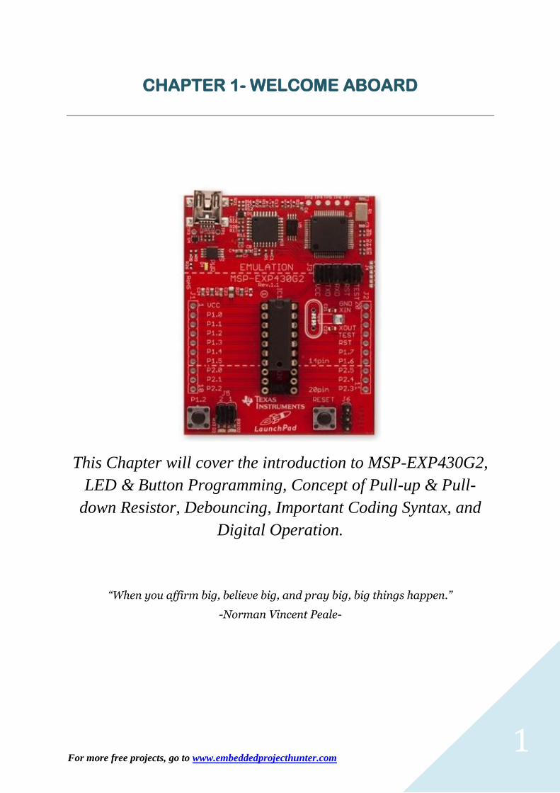
CHAPTER 1- WELCOME ABOARD
This Chapter will cover the introduction to MSP-EXP430G2,
LED & Button Programming, Concept of Pull-up & Pull-
down Resistor, Debouncing, Important Coding Syntax, and
Digital Operation.
“When you affirm big, believe big, and pray big, big things happen.”
-Norman Vincent Peale-
For more free projects, go to www.embeddedprojecthunter.com 2
1.0 Introduction
1. In MSP430 Value Line LaunchPad Development Tool, there is:
(i) 10 GPIO in a 14-pin MCU
(ii) 16 GPIO in a 20-pin MCU.
2. GPIO = General Port Input Output
3. What you want to program is the MCU (the chip)?
INPUT MCU OUTPUT
4. MSP430G2211/MSP430G2231/MSP430G2452/MSP430G2553 is some
common microcontroller chips used. MSP430G2553 is the best in term of
FLASH and RAM size.
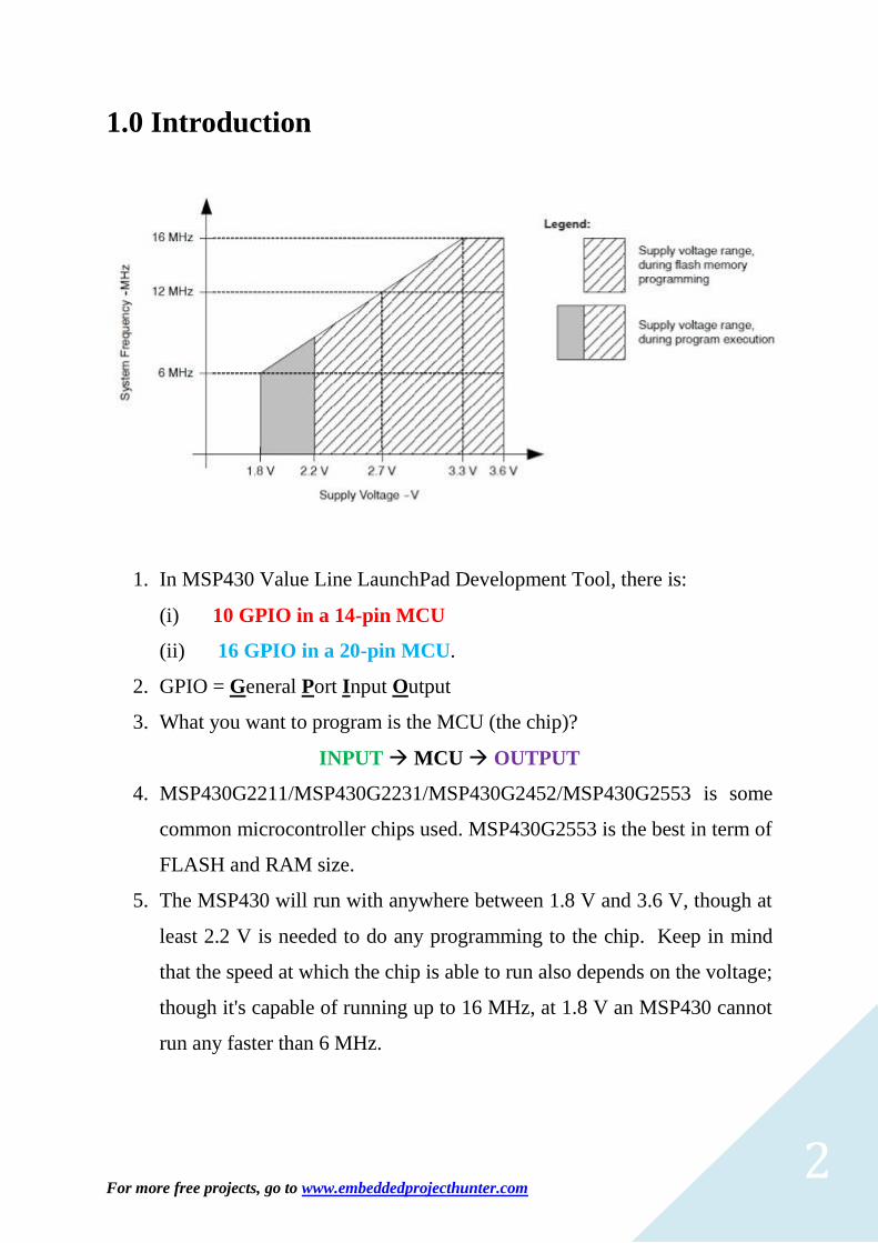
5. The MSP430 will run with anywhere between 1.8 V and 3.6 V, though at
least 2.2 V is needed to do any programming to the chip. Keep in mind
that the speed at which the chip is able to run also depends on the voltage;
though it's capable of running up to 16 MHz, at 1.8 V an MSP430 cannot
run any faster than 6 MHz.
For more free projects, go to www.embeddedprojecthunter.com 3
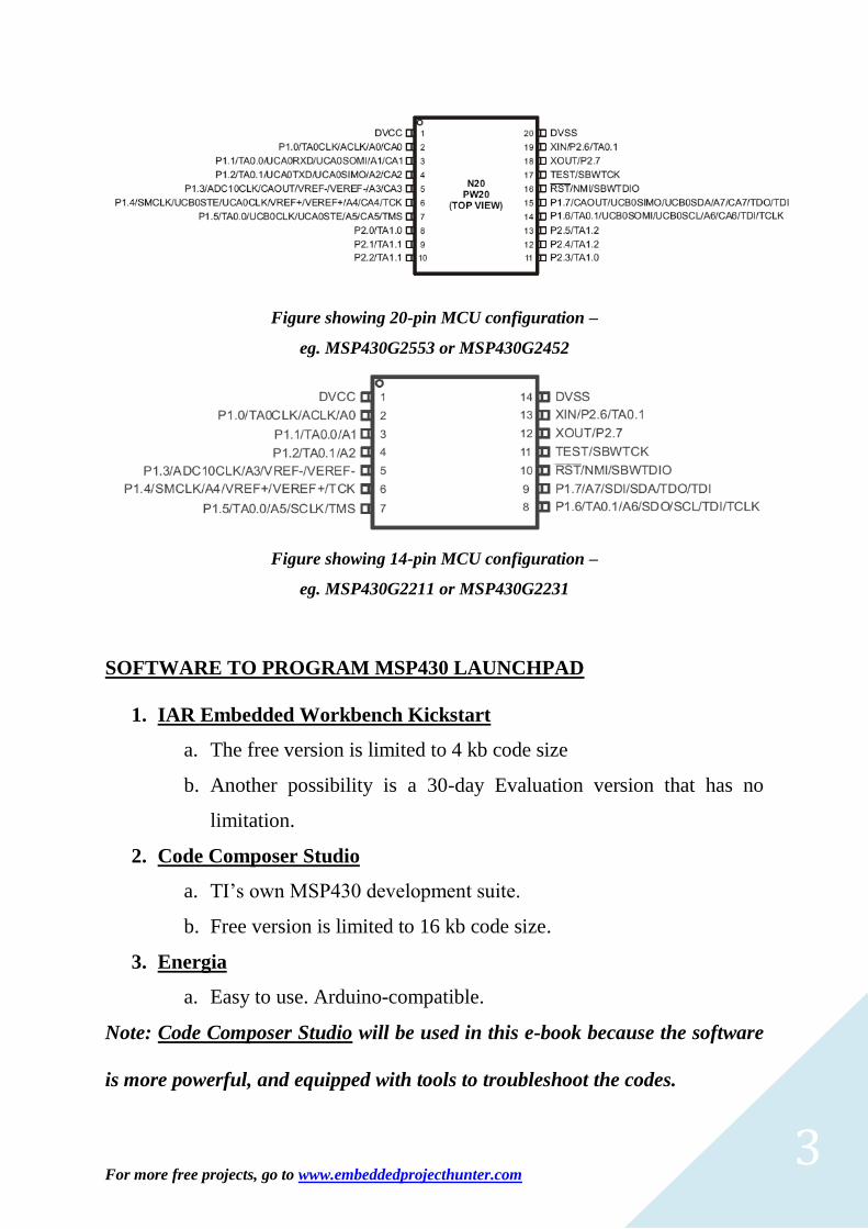
Figure showing 20-pin MCU configuration –
eg. MSP430G2553 or MSP430G2452
Figure showing 14-pin MCU configuration –
eg. MSP430G2211 or MSP430G2231
SOFTWARE TO PROGRAM MSP430 LAUNCHPAD
1. IAR Embedded Workbench Kickstart
a. The free version is limited to 4 kb code size
b. Another possibility is a 30-day Evaluation version that has no
limitation.
2. Code Composer Studio
a. TI’s own MSP430 development suite.
b. Free version is limited to 16 kb code size.
3. Energia
a. Easy to use. Arduino-compatible.
Note: Code Composer Studio will be used in this e-book because the software
is more powerful, and equipped with tools to troubleshoot the codes.

For more free projects, go to www.embeddedprojecthunter.com 4
1.1 Start Programming
“I hear and I forget; I see and I remember; I do and I understand.”
- Old Chinese Proverb-
It is always more efficient for you to move your hand, and code the MSP430 chips
by yourself. If you haven’t buy the development board, you can buy at TI store
or from any other reseller or distributor.
To download the software (Code Composer Studio), go to TI Wiki. Click to
download the latest CCS. Currently the software is supported only in Windows
and Linux.
To install CCS, simply follow the instruction on the GUI after you clicking the
installation file you downloaded. It should not be any problem installing the
software.

For more free projects, go to www.embeddedprojecthunter.com 5
After installing CCS, double-click the CCS icon. The “Workspace Launcher”
shown below will appear.
I like to create my workspace (which is the folder where all the programming
codes and necessary files saved) in the Desktop. You can save your workspace in
any other directory. Click “OK” after you have define the directory for
workspace. CCS main interface will pop-up after taking some time to setup.
Now, click on “Project” “New
CCS Project…”, then, “New CCS
Project” window will be shown.

For more free projects, go to www.embeddedprojecthunter.com 6
Step 1:
In the Target tab, key-in the
chip number that you plan to
use. If you are unsure, check
the chip label.
Step 2:
Name your project so that
you can identify and access
your project next time.
Step 3:
Click the “Finish” button to
complete the setup.
If your steps are all correct, then your project files should be visible at the Project
Explorer Window:
The main programming code that we will learn later on will be created and
amended in the main.c file. Note that the .c extension indicates that we are using
C language. We can however, program the chip using assembly language. But it
will not be covered in this e-book.
3
2
1
For more free projects, go to www.embeddedprojecthunter.com 7
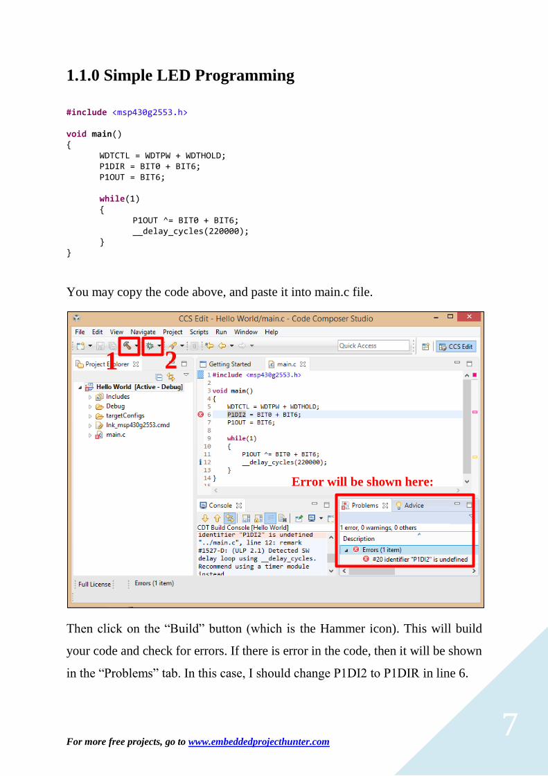
1.1.0 Simple LED Programming
#include <msp430g2553.h> void main() WDTCTL = WDTPW + WDTHOLD; P1DIR = BIT0 + BIT6; P1OUT = BIT6; while(1) P1OUT ^= BIT0 + BIT6; __delay_cycles(220000);
You may copy the code above, and paste it into main.c file.
Then click on the “Build” button (which is the Hammer icon). This will build
your code and check for errors. If there is error in the code, then it will be shown
in the “Problems” tab. In this case, I should change P1DI2 to P1DIR in line 6.
1 2
Error will be shown here:
For more free projects, go to www.embeddedprojecthunter.com 8
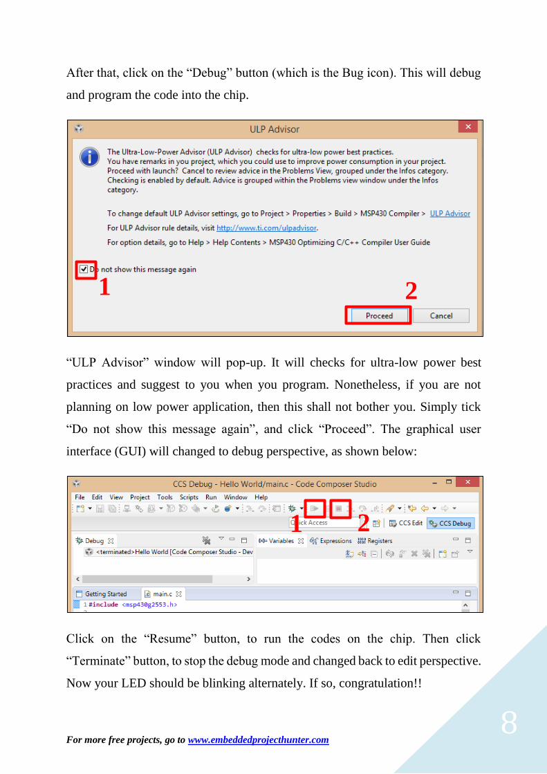
After that, click on the “Debug” button (which is the Bug icon). This will debug
and program the code into the chip.
“ULP Advisor” window will pop-up. It will checks for ultra-low power best
practices and suggest to you when you program. Nonetheless, if you are not
planning on low power application, then this shall not bother you. Simply tick
“Do not show this message again”, and click “Proceed”. The graphical user
interface (GUI) will changed to debug perspective, as shown below:
Click on the “Resume” button, to run the codes on the chip. Then click
“Terminate” button, to stop the debug mode and changed back to edit perspective.
Now your LED should be blinking alternately. If so, congratulation!!
1 2
1 2

For more free projects, go to www.embeddedprojecthunter.com 9
Code Explanation:
Code: Explanation: #include <msp430g2553.h> Since you are using MSP430G2553 chip, then
you should include all the standard register and
bit definition for the microcontroller. The .h
extension indicates that this is the header file for
the chip. void main() All the main codes are written in side main().
This is the standard format for C Language. You
may learn more in C Language text books or
webpage. WDTCTL = WDTPW + WDTHOLD; Watchdog Timer control. This line is necessary
every time you program your chip if you are not
using the watchdog timer to prevent your chip
from restarting. P1DIR = BIT0 + BIT6; P1DIR Port 1 Direction
This line simply set BIT0 and BIT6 to be your
output. Since you are programming port 1 in this
case, then BIT0 and BIT6 here is referring to P1.0
and P1.6 of the chip. If you still unsure where is
this pins located, kindly look at the development
board (RED colour board). All the pins are
labelled. According to the datasheet, P1.0 and
P1.6 are connected to the red and green LED
respectively. Therefore the LED will blink based
on your programming. P1OUT = BIT6; P1OUT Port 1 Output
This line simply turn on P1.6 and thus giving
instruction to the pin to produce 3.6 V as output. while(1) C Language, while loop is normally used to run
the code inside the loop infinitely until you switch
off the power. P1OUT ^= BIT0 + BIT6; P1OUT Port 1 Output
Set the output of the pins. Note the “^” sign. It
basically means toggle, changing 0 to 1 and 1 to
0. If the LED is turned on previously, then it will
be off now, and vice versa, __delay_cycles(220000); Delay 220000 cycles. By default, one cycle need
roughly 0.9 us to execute. Thus, approximate
delay timing will be:
220000 cycles x 0.9us per cycle = 0.2 s delay

For more free projects, go to www.embeddedprojecthunter.com 10
Tips:
You might wonder is there any “shortcut” to learn the programming. Well, of
course there is. I am going to show you some useful tips in programming the chip.
If you are unsure what WDTCTL stands for, simply move your mouse pointer to
the word and wait for few second. The description will be shown just like below.
Thus, we know that WDTCTL stands for Watchdog Timer Control without really
memorising the datasheet.
If you wish to understand more about the specific code, simply press “CTRL”
while clicking on the respective code. It will bring you to the header file and show
you where it located in the library.
For more free projects, go to www.embeddedprojecthunter.com 11
1.1.1 Simple Button Programming
#include <msp430g2553.h> void main(void) WDTCTL = WDTPW + WDTHOLD; P1DIR = BIT0; P1REN = BIT3; P1OUT = BIT3; while(1) if((P1IN & BIT3)!=BIT3) __delay_cycles(220000); P1OUT ^= BIT0;
If you look at the MSP430 Development Board, there is two buttons on the board.
The left button is user-programmable button, while the right button is RESET
button. We can use the left button for variety of applications. In this example, we
will demonstrate the usability of the left button. Simply copy the code above and
paste in main.c. Repeat the steps for the first programming where you build and
debug the codes.
The left button is connected to P1.3 of the chip. Therefore, by programming P1.3
pin, the button can be controlled. In this case, there will be both input and output.
The button will be the input while the LED will be the output.
BUTTON (INPUT) MSP430 CHIP (BRAIN) LED (OUTPUT)
Expected Output:
When you click on the LEFT button, the RED LED will toggle. In other words,
the state of the LED will be changed by pressing the button.
For more free projects, go to www.embeddedprojecthunter.com 12
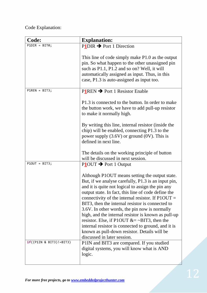
Code Explanation:
Code: Explanation: P1DIR = BIT0;
P1DIR Port 1 Direction
This line of code simply make P1.0 as the output
pin. So what happen to the other unassigned pin
such as P1.1, P1.2 and so on? Well, it will
automatically assigned as input. Thus, in this
case, P1.3 is auto-assigned as input too.
P1REN = BIT3; P1REN Port 1 Resistor Enable
P1.3 is connected to the button. In order to make
the button work, we have to add pull-up resistor
to make it normally high.
By writing this line, internal resistor (inside the
chip) will be enabled, connecting P1.3 to the
power supply (3.6V) or ground (0V). This is
defined in next line.
The details on the working principle of button
will be discussed in next session. P1OUT = BIT3; P1OUT Port 1 Output
Although P1OUT means setting the output state.
But, if we analyse carefully, P1.3 is an input pin,
and it is quite not logical to assign the pin any
output state. In fact, this line of code define the
connectivity of the internal resistor. If P1OUT =
BIT3, then the internal resistor is connected to
3.6V. In other words, the pin now is normally
high, and the internal resistor is known as pull-up
resistor. Else, if P1OUT &= ~BIT3, then the
internal resistor is connected to ground, and it is
known as pull-down resistor. Details will be
discussed in later session. if((P1IN & BIT3)!=BIT3)
P1IN and BIT3 are compared. If you studied
digital systems, you will know what is AND
logic.
For more free projects, go to www.embeddedprojecthunter.com 13
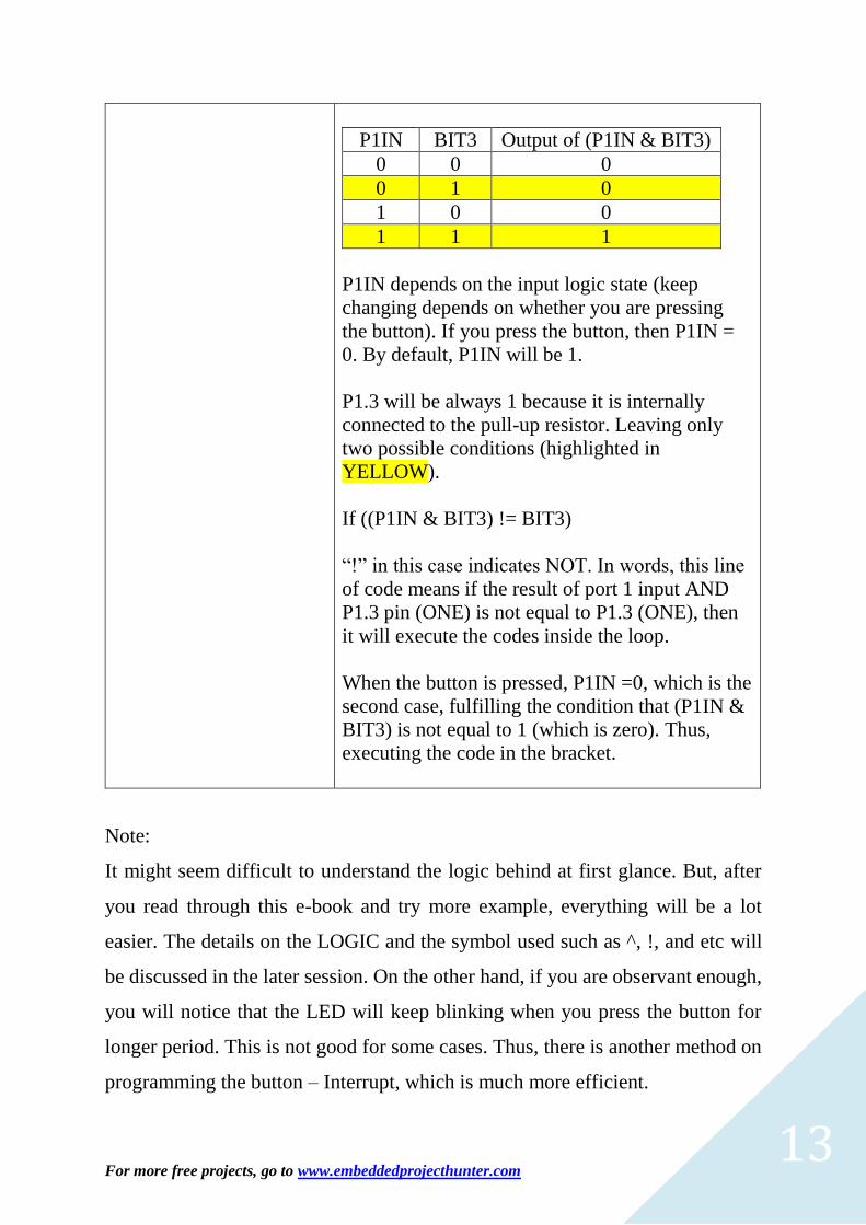
P1IN BIT3 Output of (P1IN & BIT3)
0 0 0
0 1 0
1 0 0
1 1 1
P1IN depends on the input logic state (keep
changing depends on whether you are pressing
the button). If you press the button, then P1IN =
0. By default, P1IN will be 1.
P1.3 will be always 1 because it is internally
connected to the pull-up resistor. Leaving only
two possible conditions (highlighted in
YELLOW).
If ((P1IN & BIT3) != BIT3)
“!” in this case indicates NOT. In words, this line
of code means if the result of port 1 input AND
P1.3 pin (ONE) is not equal to P1.3 (ONE), then
it will execute the codes inside the loop.
When the button is pressed, P1IN =0, which is the
second case, fulfilling the condition that (P1IN &
BIT3) is not equal to 1 (which is zero). Thus,
executing the code in the bracket.
Note:
It might seem difficult to understand the logic behind at first glance. But, after
you read through this e-book and try more example, everything will be a lot
easier. The details on the LOGIC and the symbol used such as ^, !, and etc will
be discussed in the later session. On the other hand, if you are observant enough,
you will notice that the LED will keep blinking when you press the button for
longer period. This is not good for some cases. Thus, there is another method on
programming the button – Interrupt, which is much more efficient.
For more free projects, go to www.embeddedprojecthunter.com 14
1.1.2 Button Programming with Interrupt
#include <msp430g2553.h> void main(void) WDTCTL = WDTPW + WDTHOLD; P1DIR = BIT6; P1REN = BIT3; P1OUT = BIT3; P1IE = BIT3; __enable_interrupt(); while(1) #pragma vector=PORT1_VECTOR __interrupt void Port_1(void) __delay_cycles(500000); P1OUT ^= BIT6; P1IFG = ~BIT3;
In this example, a better and more stable programming code is demonstrated.
GREEN LED is used instead of RED LED as compared to previous example.
Note that there is another function introduced, which is the Port_1(void). “void”
means nothing.
Code Explanation:
Code: Explanation: P1IE = BIT3; P1IE Port 1 Interrupt Enable
This line of code simply make P1.3 as an
interrupt pin. Any changes of this pin will trigger
the interrupt.
__enable_interrupt();
Even though P1.3 is interrupt-enabled, but the
interrupt algorithm is not initialized yet. This line
will enable the interrupt in the codes.
#pragma vector=PORT1_VECTOR __interrupt void Port_1(void)
PORT1_VECTOR indicates the interrupt vector
that we use, which is Port 1, since P1.3 is in Port
For more free projects, go to www.embeddedprojecthunter.com 15
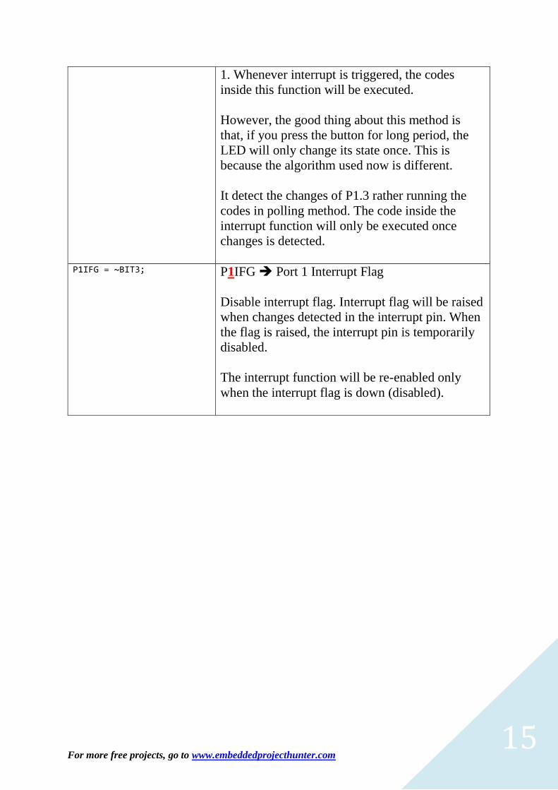
1. Whenever interrupt is triggered, the codes
inside this function will be executed.
However, the good thing about this method is
that, if you press the button for long period, the
LED will only change its state once. This is
because the algorithm used now is different.
It detect the changes of P1.3 rather running the
codes in polling method. The code inside the
interrupt function will only be executed once
changes is detected.
P1IFG = ~BIT3; P1IFG Port 1 Interrupt Flag
Disable interrupt flag. Interrupt flag will be raised
when changes detected in the interrupt pin. When
the flag is raised, the interrupt pin is temporarily
disabled.
The interrupt function will be re-enabled only
when the interrupt flag is down (disabled).

For more free projects, go to www.embeddedprojecthunter.com 16
1.2 What is Pull-Up and Pull-Down Resistor?
Let’s think a bit about what happens when the system is powered up. Here, the
switch is normally open and the P2.0 is left floating and this is very bad. When
the switch is pressed, P2.0 is connected to ground. There is no clear voltage
transition because the initial condition is floating. Similar designs have been used
by many newcomers and should be avoided. A design such as that is possible if
there is an internal pull-up resistor.
Let’s analyze the second case (b), where the designer included an external pull-
up resistor. Here, the switch is also open initially, but P2.0 is connected to VCC
through the resistor. The resistor limits the current significantly (considering a
resistor with 100k or so). When the user presses the switch, one end of the resistor
and P2.0 get connected to ground. P2.0 experiences a transition from high to low.
The resistor has current flowing through it and although it is wasted as heat, it is
very small and lasts for only a few moments for the duration of the switch press.
Many microcontrollers include internal pull-up or even pull-down, which
free the designer from having to include them. In this case, simply connect the
button to either VCC or GND and it should work.

For more free projects, go to www.embeddedprojecthunter.com 17
1.3 Debounce… Bounce... Bounce…
Up to now, we’ve assumed that the switch is perfect. In reality that is not so. The
mechanical construction of the switch results in internal vibrations (bouncing) in
which the metals bounce until they settle and make contact. During this time, a
switch can result in many connections/disconnections that a microcontroller will
interpret as multiple presses when in fact a user only pressed once. The end result
is that multiple interrupts will be generated and can cause issues in the end
application. What to do? In general there are two approaches to doing
debouncing: Analog and Software.
The analog approach uses a capacitor and a schmitt trigger. When a capacitor is
added to the switch input, the capacitor is pulled high by the pull-up resistor and
therefore is charged. When the key is pressed, the capacitor will resist the change
in voltage (the switch is grounding the input). The capacitor will discharge,
preventing the bouncing of the switch contact. This depends heavily on the size
of the capacitor and resistor (on their RC time constant). The larger the RC time
constant, the more bouncing will be reduced. However, the switches
responsiveness will be affected. When the user releases the button, the capacitor

For more free projects, go to www.embeddedprojecthunter.com 18
slowly charges and therefore any bounces are also filtered. However, because of
the slow transition, the I/O input will transition in an unknown state which could
cause issues. A schmitt trigger is then required to avoid any problems. This is
typically not an issue because the MSP430 includes a schmitt trigger at the I/O
inputs.
The other solution that can be done is in software. Using interrupts we can detect
the switches high to low and low to high transitions and ignore those that are
inside of the bounce window by waiting for a set amount of time (using a timer
or a for loop to waste cycles) before accepting new transitions as actual user
switch presses. The amount of time to wait depends on the switch to be used, but
40ms is a safe bet in many cases. If you can’t wait that long, measure the bouncing
time using an oscilloscope and create a worse case estimate. We must also ensure
that the first bounce of the switch was not a momentary malfunction (as could be
the case if the switch is malfunctioning or the board was dropped creating an
accidental contact.
For more free projects, go to www.embeddedprojecthunter.com 19
1.4 Important Coding Syntax
PxIN
The input register for a port is a read-only value. When a pin is selected to be an
input, reading the value of the bit tells you the voltage currently on that pin. The
entire byte PxIN reads the value of all of the inputs on that port at once. Keep in
mind this is a digital system, so there are only two values that can be read; a 0 or
a 1. These values correspond to the voltages on Vss (0) and Vcc (1), which are
generaly 0 V and between 1.8 and 3.6 V respectively. There is a particular
threshold built into the device such that any voltage over that value is read as a 1
and any voltage read below is read as a 0. To prevent any damage to the chip,
you should certainly never try to read any voltages outside the range between Vss
and Vcc directly.
PxOUT
The output register for a port is writeable. When a pin is selected to be an output,
we can change the voltage on that pin by writing a 0 or a 1 to its corresponding
bit in PxOUT. Like the input, a 0 corresponds to the voltage on Vss, and a 1
corresponds to the voltage on Vcc.
PxDIR
The direction register determines whether a pin is an input (bit is low, or 0) or an
output (bit is high, or 1). At the beginning of your program, you should configure
the port pins to their values as inputs or outputs. That's not to say you can't change
a pin's behavior in the middle of your program, of course.
For more free projects, go to www.embeddedprojecthunter.com 20
PxIE, PxIES, and PxIFG
These three registers are the interrupt enable, interrupt edge select, and interrupt
flag registers for the ports. We'll look at these three registers together, as they
work together. You can use the port pins as a way to flag special circumstances
to the processor and trigger an interrupt. For now, think of an interrupt as a
message to the CPU to hold on what it's currently doing and take care of the
special circumstance. Once the interrupt has been satisfied, the CPU returns to
where it was before. You enable this behavior by setting the PxIE bit for the pin
being used to 1. PxIES bits determine if the flag is triggered by the pin going
from 0 to 1 (IES bit set to 0) or from 1 to 0 (IES bit set to 1). In other words, a
flag is triggered when it detects a positively sloped, rising edge or a negatively
sloped, falling edge. When the interrupt is triggered, it sets the corresponding bit
in PxIFG.
PxSEL
Looking back at the pinout diagram on page 3, you can see that most of the port
pins have multiple functions. The selection register determines what function a
pin takes on. The default function is listed first, so P1 defaults to general I/O
pins, whereas the P2 pins default to connections to a crystal oscillator. Changing
the bits in PxSEL changes the behavior of the pins. We'll look at the particular
settings later; for now, plan on using the default values in PxSEL.
PxREN
The resistor enable register is a very useful feature for the ports. Sometimes it is
helpful to pull the voltage up to Vcc or down to Vss, such as when you attach a
push button to a pin. The resistor enable register lets you turn on that
ability. When a PxREN bit is enabled, you can select it as a pull-up or pull-down
resistor by setting the corresponding bit in PxOUT, 1 for up, 0 for down.
For more free projects, go to www.embeddedprojecthunter.com 21
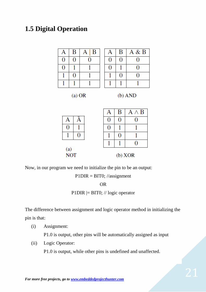
1.5 Digital Operation
Now, in our program we need to initialize the pin to be an output:
P1DIR = BIT0; //assignment
OR
P1DIR |= BIT0; // logic operator
The difference between assignment and logic operator method in initializing the
pin is that:
(i) Assignment:
P1.0 is output, other pins will be automatically assigned as input
(ii) Logic Operator:
P1.0 is output, while other pins is undefined and unaffected.

For more free projects, go to www.embeddedprojecthunter.com 22
To turn off every pins:
P1OUT = 0;
To turn the RED LED on:
P1OUT |= BIT0;
To turn the RED LED off:
P1OUT &= ~BIT0;
To toggle its state (off if on, on if off):
P1OUT ^= BIT0;
Let’s try another example:
First, let's configure the two pins as outputs with an initial state off:
P1DIR = BIT0 + BIT6;
P1OUT = 0;
We can turn each one on and off individually:
P1OUT |= BIT0; // P1.0 on
P1OUT &= ~BIT0; // P1.0 off
P1OUT |= BIT6; // P1.6 on
P1OUT &= ~BIT6; // P1.6 off
Or we can turn them on and off together:
P1OUT |= BIT0 + BIT6; // both on
P1OUT &= ~(BIT0 + BIT6); // both off
And finally, toggle them simultaneously:
P1OUT ^= BIT0 + BIT6; // toggle both
Note: Put some delay in between the lines to observe the state changes.
For more free projects, go to www.embeddedprojecthunter.com 23
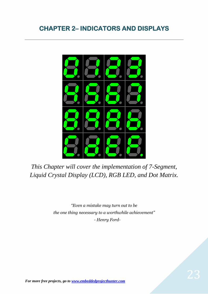
CHAPTER 2– INDICATORS AND DISPLAYS
This Chapter will cover the implementation of 7-Segment,
Liquid Crystal Display (LCD), RGB LED, and Dot Matrix.
“Even a mistake may turn out to be
the one thing necessary to a worthwhile achievement”
- Henry Ford-
For more free projects, go to www.embeddedprojecthunter.com 24
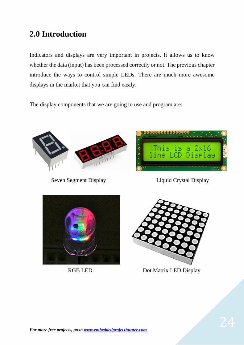
2.0 Introduction
Indicators and displays are very important in projects. It allows us to know
whether the data (input) has been processed correctly or not. The previous chapter
introduce the ways to control simple LEDs. There are much more awesome
displays in the market that you can find easily.
The display components that we are going to use and program are:
Seven Segment Display Liquid Crystal Display
RGB LED Dot Matrix LED Display

For more free projects, go to www.embeddedprojecthunter.com 25
2.1 Seven-Segment Display
Seven-Segment display got their name because of it consists of seven segments
LED that can be controlled to display variety of numbers and pattern. So how
many LEDs are there in the seven-segment? Seven… Nope… In total there are
eight LEDs which includes the small dots at the bottom right. Also, we have two
types of seven-segment – Common Cathode and Common Anode. Common
Cathode means all the LEDs share the same ground, while LEDs on common
anode seven-segment display share the same power supply as shown in the figure
below.
In this chapter, we are going to use common cathode seven-segment display.
Basically, we are just going to on and off the LEDs just like what we do in the
previous chapter, but in a more systematic way.
For more free projects, go to www.embeddedprojecthunter.com 26
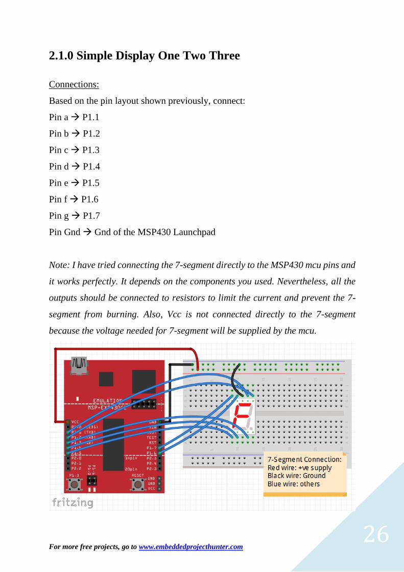
2.1.0 Simple Display One Two Three
Connections:
Based on the pin layout shown previously, connect:
Pin a P1.1
Pin b P1.2
Pin c P1.3
Pin d P1.4
Pin e P1.5
Pin f P1.6
Pin g P1.7
Pin Gnd Gnd of the MSP430 Launchpad
Note: I have tried connecting the 7-segment directly to the MSP430 mcu pins and
it works perfectly. It depends on the components you used. Nevertheless, all the
outputs should be connected to resistors to limit the current and prevent the 7-
segment from burning. Also, Vcc is not connected directly to the 7-segment
because the voltage needed for 7-segment will be supplied by the mcu.
For more free projects, go to www.embeddedprojecthunter.com 27
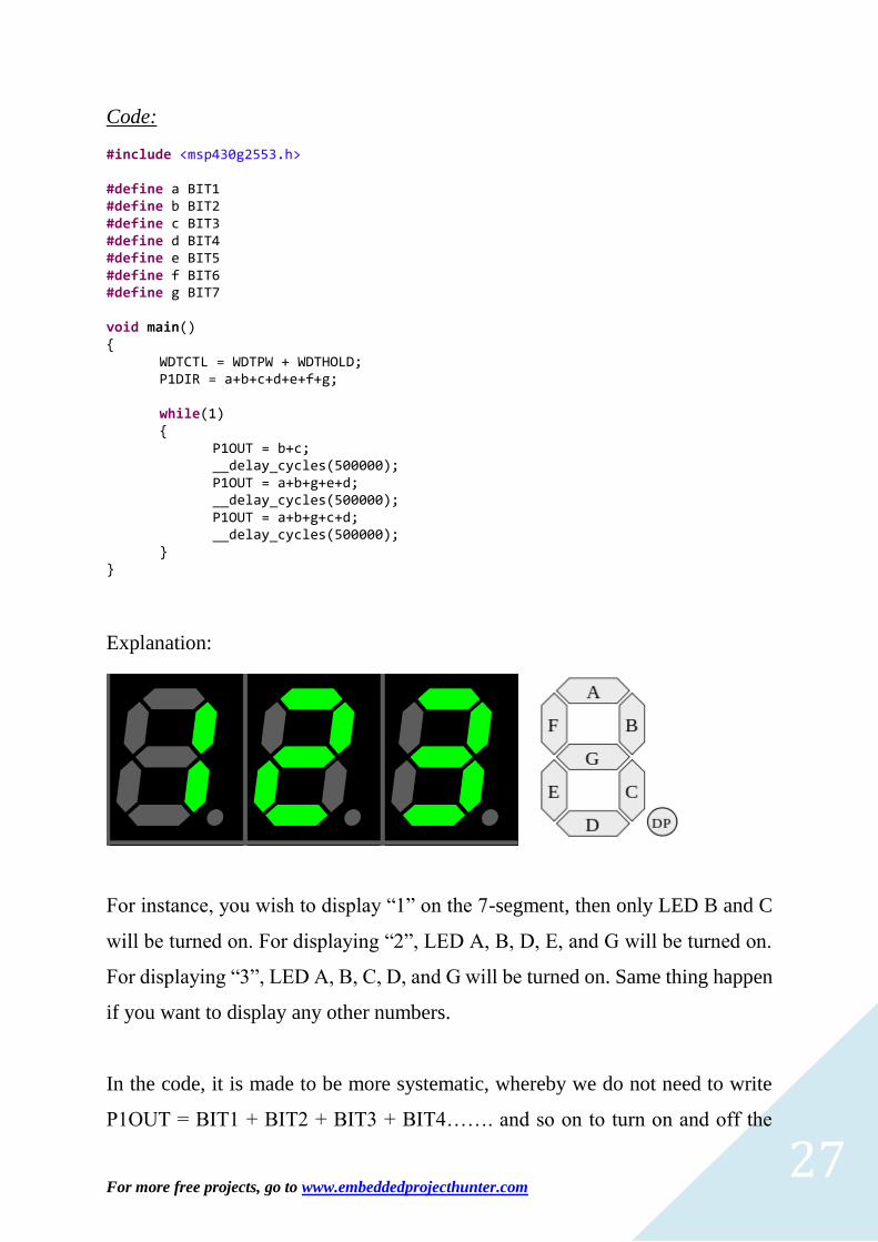
Code: #include <msp430g2553.h> #define a BIT1 #define b BIT2 #define c BIT3 #define d BIT4 #define e BIT5 #define f BIT6 #define g BIT7 void main() WDTCTL = WDTPW + WDTHOLD; P1DIR = a+b+c+d+e+f+g; while(1) P1OUT = b+c; __delay_cycles(500000); P1OUT = a+b+g+e+d; __delay_cycles(500000); P1OUT = a+b+g+c+d; __delay_cycles(500000);
Explanation:
For instance, you wish to display “1” on the 7-segment, then only LED B and C
will be turned on. For displaying “2”, LED A, B, D, E, and G will be turned on.
For displaying “3”, LED A, B, C, D, and G will be turned on. Same thing happen
if you want to display any other numbers.
In the code, it is made to be more systematic, whereby we do not need to write
P1OUT = BIT1 + BIT2 + BIT3 + BIT4……. and so on to turn on and off the

For more free projects, go to www.embeddedprojecthunter.com 28
LEDs. In this example, we use #define to represent BIT1 with “a”, BIT2 with “b”
and the list continues. Hence, our code will looks more organised and easier to
interpret. For example, P1OUT = b + c; simply means that LED B and C are
turned on, other pins are off, which eventually displaying “1” on the 7-segment.
Expected Output:
It continually display from 1 to 3 then start all over again and again and again
(since it is in while loop).
2.1.1 Seven-segment Extra Training
Task 1:
Modify the code to make the 7-Seg to count from 0-9 continuously.
Task 2:
Is there any way of reducing the number of lines in the code?? For sure, there is
a way!!
By using array!! Single dimension array is sufficient enough to do the work. As
for now, for the sake of simplicity and to meet the purpose of learning, the sample
code is given.
Task 3:
How to make the 7 segment to change the number every time you pressed the
button? Referring to the previous examples, try to write your own code before
looking at the answer code.
Answer for Task 1:
#include <msp430g2553.h>
For more free projects, go to www.embeddedprojecthunter.com 29
#define a BIT1 #define b BIT2 #define c BIT3 #define d BIT4 #define e BIT5 #define f BIT6 #define g BIT7 void main() WDTCTL = WDTPW + WDTHOLD; P1DIR = a+b+c+d+e+f+g; while(1) P1OUT = a+b+c+d+e+f; __delay_cycles(500000); P1OUT = b+c; __delay_cycles(500000); P1OUT = a+b+g+e+d; __delay_cycles(500000); P1OUT = a+b+g+c+d; __delay_cycles(500000); P1OUT = f+g+b+c; __delay_cycles(500000); P1OUT = a+f+g+c+d; __delay_cycles(500000); P1OUT = a+f+e+d+c+g; __delay_cycles(500000); P1OUT = a+b+c; __delay_cycles(500000); P1OUT = a+b+c+d+e+f+g; __delay_cycles(500000); P1OUT = a+b+c+d+f+g; __delay_cycles(500000);
Remarks:
Finally some hands-on work can be done! This code is for common cathode 7-
Seg display. Good Luck Trying! Isn’t it easy?
Answer for Task 2:
#include <msp430g2553.h>
For more free projects, go to www.embeddedprojecthunter.com 30
#define a BIT1 #define b BIT2 #define c BIT3 #define d BIT4 #define e BIT5 #define f BIT6 #define g BIT7 int display[10]=a+b+c+d+e+f, b+c, a+b+g+e+d, a+b+g+c+d, f+g+b+c, a+f+g+c+d, a+f+e+d+c+g, a+b+c, a+b+c+d+e+f+g, a+b+c+d+f+g; int n = 0; void main() WDTCTL = WDTPW + WDTHOLD; P1DIR = a+b+c+d+e+f+g; while(1) P1OUT = display[n]; __delay_cycles(500000); n++; if (n==10) n=0;
Remarks:
Bonus for all of you~~ Simplified and more efficient code for displaying 0 to 9 by
using array!! Remember~ By producing same output, the shorter your code, the
better you are!!
(This code is for common cathode 7-Seg display.)
Answer for Task 3:
#include <msp430g2553.h>
For more free projects, go to www.embeddedprojecthunter.com 31
#define a BIT0 #define b BIT1 #define c BIT2 #define d BIT4 #define e BIT5 #define f BIT6 #define g BIT7 int display[10]=a+b+c+d+e+f, b+c, a+b+g+e+d, a+b+g+c+d, f+g+b+c, a+f+g+c+d, a+f+e+d+c+g, a+b+c, a+b+c+d+e+f+g, a+b+c+d+f+g; int n = 0; void main() WDTCTL = WDTPW + WDTHOLD; P1DIR = a+b+c+d+e+f+g; P1REN = BIT3; P1OUT = BIT3; while(1) if((P1IN & BIT3)!=BIT3) __delay_cycles(220000); P1OUT &= ~(a+b+c+d+e+f+g); P1OUT |= display[n]; n++; if (n==10) n=0;
Remarks:
Control button is added. Noted that P1.3 is connected to the button, thus the same
pin cannot be used to control the 7-segment. Hence, in this case, P1.0 is used.
When you pressed the button, the number increase by 1. It is now become a digital
counter!! Well done!! But it is using polling method, try it using interrupt method
instead~
(This code is for common cathode 7-Seg display.)
For more free projects, go to www.embeddedprojecthunter.com 32
2.1.2 Persistence of Vision (POV) Implementation
Hope that you enjoy learning so far. However, by controlling single 7-segment
we needed seven GPIO pins from the microcontroller. How many pins do we
need if we are going to control four 7-segment together? By simple logic, 4
multiply by 7 is 28 pins. Well, it would cost you quite a lot if you really are going
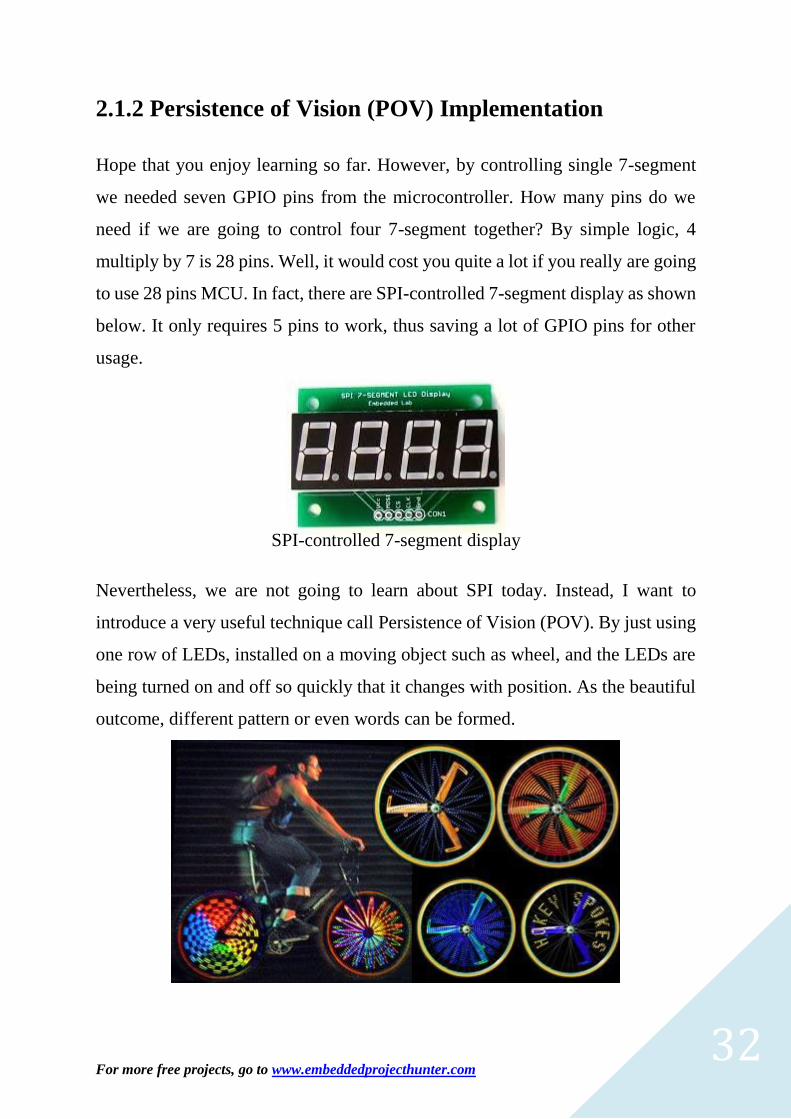
to use 28 pins MCU. In fact, there are SPI-controlled 7-segment display as shown
below. It only requires 5 pins to work, thus saving a lot of GPIO pins for other
usage.
Nevertheless, we are not going to learn about SPI today. Instead, I want to
introduce a very useful technique call Persistence of Vision (POV). By just using
one row of LEDs, installed on a moving object such as wheel, and the LEDs are
being turned on and off so quickly that it changes with position. As the beautiful
outcome, different pattern or even words can be formed.
SPI-controlled 7-segment display
For more free projects, go to www.embeddedprojecthunter.com 33
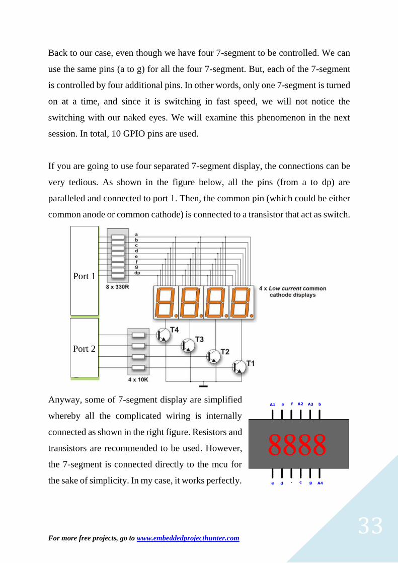
Back to our case, even though we have four 7-segment to be controlled. We can
use the same pins (a to g) for all the four 7-segment. But, each of the 7-segment
is controlled by four additional pins. In other words, only one 7-segment is turned
on at a time, and since it is switching in fast speed, we will not notice the
switching with our naked eyes. We will examine this phenomenon in the next
session. In total, 10 GPIO pins are used.
If you are going to use four separated 7-segment display, the connections can be
very tedious. As shown in the figure below, all the pins (from a to dp) are
paralleled and connected to port 1. Then, the common pin (which could be either
common anode or common cathode) is connected to a transistor that act as switch.
Anyway, some of 7-segment display are simplified
whereby all the complicated wiring is internally
connected as shown in the right figure. Resistors and
transistors are recommended to be used. However,
the 7-segment is connected directly to the mcu for
the sake of simplicity. In my case, it works perfectly.
Port 1
Port 2

For more free projects, go to www.embeddedprojecthunter.com 34
Port 1 is connecting to a,b,c,d,e,f, and g, while Port 2 is connecting to A1, A2,
A3, and A4. Note that no Vcc or ground is connected directly to the 7-segment
since the 7-segment is powered up by the output pin of the mcu.
Task:
Besides numbers, we can display some of the alphebets too, such as A, b, C, d,
E, F, g, H, I, J, L, O, P, S, U, and y. In this example, we will display some random
alphebets on the 7-segment, let’s try U, C, S, and I. Also, we will be using
common-anode 7-segment display so that both types of display will be learned.
For more free projects, go to www.embeddedprojecthunter.com 35
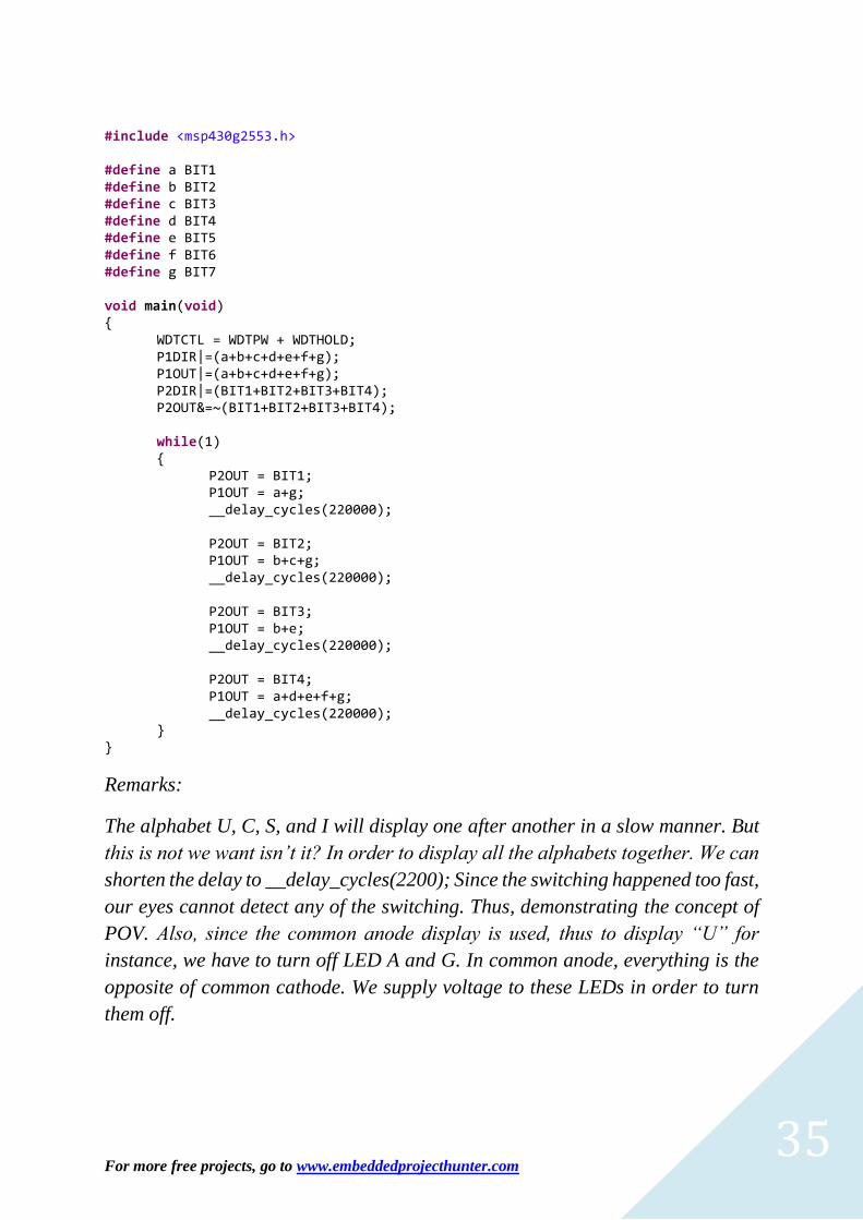
#include <msp430g2553.h> #define a BIT1 #define b BIT2 #define c BIT3 #define d BIT4 #define e BIT5 #define f BIT6 #define g BIT7 void main(void) WDTCTL = WDTPW + WDTHOLD; P1DIR|=(a+b+c+d+e+f+g); P1OUT|=(a+b+c+d+e+f+g); P2DIR|=(BIT1+BIT2+BIT3+BIT4); P2OUT&=~(BIT1+BIT2+BIT3+BIT4); while(1) P2OUT = BIT1; P1OUT = a+g; __delay_cycles(220000); P2OUT = BIT2; P1OUT = b+c+g; __delay_cycles(220000); P2OUT = BIT3; P1OUT = b+e; __delay_cycles(220000); P2OUT = BIT4; P1OUT = a+d+e+f+g; __delay_cycles(220000);
Remarks:
The alphabet U, C, S, and I will display one after another in a slow manner. But
this is not we want isn’t it? In order to display all the alphabets together. We can
shorten the delay to __delay_cycles(2200); Since the switching happened too fast,
our eyes cannot detect any of the switching. Thus, demonstrating the concept of
POV. Also, since the common anode display is used, thus to display “U” for
instance, we have to turn off LED A and G. In common anode, everything is the
opposite of common cathode. We supply voltage to these LEDs in order to turn
them off.
For more free projects, go to www.embeddedprojecthunter.com 36
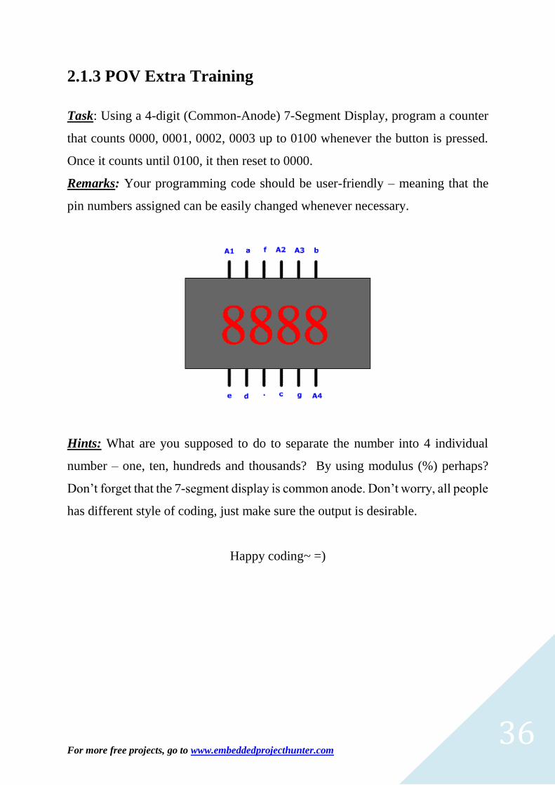
2.1.3 POV Extra Training
Task: Using a 4-digit (Common-Anode) 7-Segment Display, program a counter
that counts 0000, 0001, 0002, 0003 up to 0100 whenever the button is pressed.
Once it counts until 0100, it then reset to 0000.
Remarks: Your programming code should be user-friendly – meaning that the
pin numbers assigned can be easily changed whenever necessary.
Hints: What are you supposed to do to separate the number into 4 individual
number – one, ten, hundreds and thousands? By using modulus (%) perhaps?
Don’t forget that the 7-segment display is common anode. Don’t worry, all people
has different style of coding, just make sure the output is desirable.
Happy coding~ =)

For more free projects, go to www.embeddedprojecthunter.com 37
Answer:
#include <msp430g2553.h> #define a BIT0 #define b BIT1 #define c BIT2 #define d BIT4 #define e BIT5 #define f BIT6 #define g BIT7 #define zero a+b+c+d+e+f #define one b+c #define two a+b+d+e+g #define three a+b+c+d+g #define four b+c+f+g #define five a+c+d+f+g #define six a+c+d+e+f+g #define seven a+b+c #define eight a+b+c+d+e+f+g #define nine a+b+c+d+f+g #define all a+b+c+d+e+f+g unsigned char LED[10] = zero,one,two,three,four,five,six,seven,eight,nine; unsigned char n=0; unsigned char thousand; unsigned char hundred; unsigned char ten; unsigned char unit; void main(void) WDTCTL = WDTPW + WDTHOLD; P1DIR = a+b+c+d+e+f+g; //Set all Port 1 as Output, except BIT3 P1REN = BIT3; //Enable P1.3 Internal Resistor P1OUT = BIT3 + a+b+c+d+e+f+g; //Set P1.3 as Pull Up P2DIR = a+b+c+d; //set all P2.0, P2.1, P2.2, P2.4 as output too while(1) if((P1IN & BIT3)!=BIT3) __delay_cycles(220000);//Software Debounce n++; if (n>100) n=0; else thousand = (n/1000)%10; P2OUT = a; P1OUT |= all; P1OUT &= ~LED[thousand]; __delay_cycles(2200); hundred = (n/100)%10;
For more free projects, go to www.embeddedprojecthunter.com 38
P2OUT = b; P1OUT |= all; P1OUT &= ~LED[hundred]; __delay_cycles(2200); ten = (n/10)%10; P2OUT = c; P1OUT |= all; P1OUT &= ~LED[ten]; __delay_cycles(2200); unit = n%10; P2OUT = d; P1OUT |= all; P1OUT &= ~LED[unit]; __delay_cycles(2200);
Remarks:
4-Digit Digital Counter~ Finally, nice and perfect programming to count from 0
to 100 by pressing the button. Hope you enjoy learning it.
(This code is for common-anode 7-Seg)

For more free projects, go to www.embeddedprojecthunter.com 39
2.2 RGB LED
RGB LED stands for Red, Green, and Blue LED. In short, it is a 3-in-1 LED.
Basically, it operates just like the ordinary LED. It has two types. Common
cathode and common anode. In this case, when the RGB cathode are connected
to ground, then the respective colour will be lighted. The advantage of using this
type of LED is its compact size. If your system need three different coloured LED
as indicators. RGB LED may be your better choice.
2.3 Dot Matrix
The figure above shown the pin layout of a dot matrix. Your component might
have different pin configuration. Anyway, you have to determine the pins that
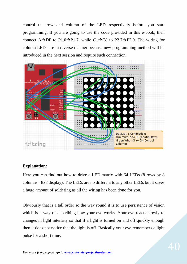
For more free projects, go to www.embeddedprojecthunter.com 40
control the row and column of the LED respectively before you start
programming. If you are going to use the code provided in this e-book, then
connect ADP to P1.0P1.7, while C1C8 to P2.7P2.0. The wiring for
column LEDs are in reverse manner because new programming method will be
introduced in the next session and require such connection.
Explanation:
Here you can find out how to drive a LED matrix with 64 LEDs (8 rows by 8
columns - 8x8 display). The LEDs are no different to any other LEDs but it saves
a huge amount of soldering as all the wiring has been done for you.
Obviously that is a tall order so the way round it is to use persistence of vision
which is a way of describing how your eye works. Your eye reacts slowly to
changes in light intensity so that if a light is turned on and off quickly enough
then it does not notice that the light is off. Basically your eye remembers a light
pulse for a short time.
For more free projects, go to www.embeddedprojecthunter.com 41
The approximate time is 20ms so if the light is turned on at a frequency >50Hz
(1/20ms) then your eye will not notice any flicker at all. Multiplexing uses this
fact to reduce the number of pins needed to drive an LED display. You can do
this by splitting the 64 led display into 8 rows and 8 columns which lets you drive
it using 8 row outputs and 8 column outputs. In fact the 8x8 led matrix block used
here has all the LEDs arranged in this way already. Each row is driven in turn and
as long as all of the rows are driven within a time period of 20ms it will appear
as though the LEDs are on continuously.
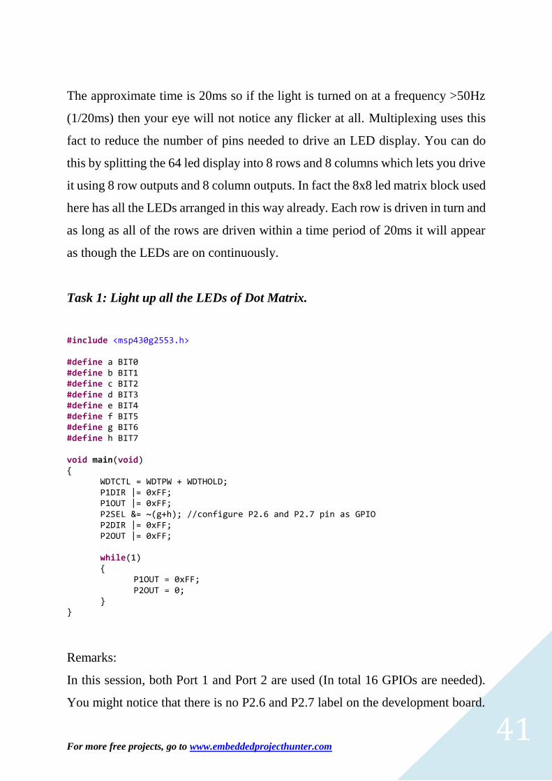
Task 1: Light up all the LEDs of Dot Matrix.
#include <msp430g2553.h> #define a BIT0 #define b BIT1 #define c BIT2 #define d BIT3 #define e BIT4 #define f BIT5 #define g BIT6 #define h BIT7 void main(void) WDTCTL = WDTPW + WDTHOLD; P1DIR |= 0xFF; P1OUT |= 0xFF; P2SEL &= ~(g+h); //configure P2.6 and P2.7 pin as GPIO P2DIR |= 0xFF; P2OUT |= 0xFF; while(1) P1OUT = 0xFF; P2OUT = 0;
Remarks:
In this session, both Port 1 and Port 2 are used (In total 16 GPIOs are needed).
You might notice that there is no P2.6 and P2.7 label on the development board.

For more free projects, go to www.embeddedprojecthunter.com 42
According to the datasheet, P2.6 and P2.7 share the same pin with XIN and
XOUT respectively. Since GPIO is NOT the primary function of these two pins,
additional P2SEL code is needed to configure the pins.
What is 0xFF? Up to this session, we know that we can use define “a” to be BIT0
in order to shorten and organize the code. Yet, it is cumbersome to write P1OUT
= a + b + c + d + e + f + g + h. Hence, it is better to utilize the hexadecimal (HEX)
format, which is P1OUT = 0xFF, which basically mean the same thing. How does
it works then?
Registers BIT7 BIT6 BIT5 BIT4 BIT3 BIT2 BIT1 BIT0
State 1 1 0 0 1 0 1 1
In HEX C B
Let say we would like to turn on BIT7, BIT6, BIT3, BIT1, and BIT0. In the old
method, we would write P1OUT = BIT7 + BIT6 + BIT3 + BIT1 + BIT0. In
binary, the state would be 110010112, which is equivalent to CB16 in hexadecimal.
Thus, we can then program the code as P1OUT = 0xCB, where “0x” means
hexadecimal, “0b” for binary and so on.
More example:
1010 10112 AB16
1111 01012 F516
P2.6 P2.7
LSB MSB
For more free projects, go to www.embeddedprojecthunter.com 43
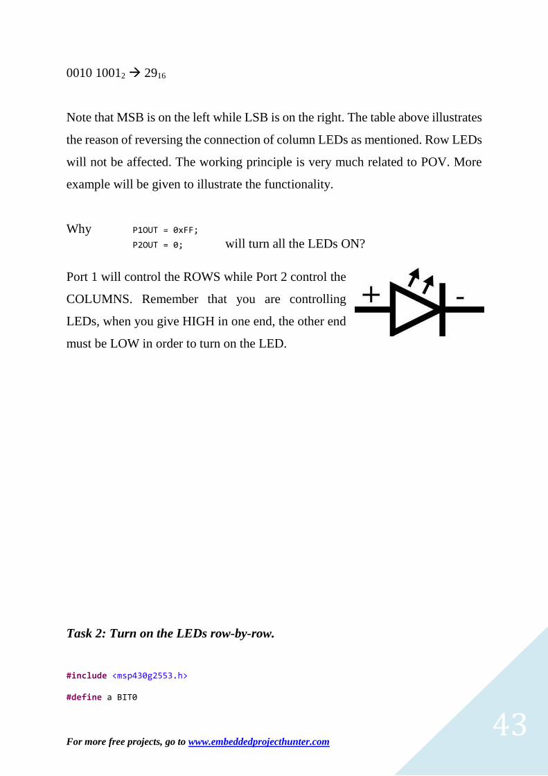
0010 10012 2916
Note that MSB is on the left while LSB is on the right. The table above illustrates
the reason of reversing the connection of column LEDs as mentioned. Row LEDs
will not be affected. The working principle is very much related to POV. More
example will be given to illustrate the functionality.
Why P1OUT = 0xFF;
P2OUT = 0; will turn all the LEDs ON?
Port 1 will control the ROWS while Port 2 control the
COLUMNS. Remember that you are controlling
LEDs, when you give HIGH in one end, the other end
must be LOW in order to turn on the LED.
Task 2: Turn on the LEDs row-by-row.
#include <msp430g2553.h> #define a BIT0
For more free projects, go to www.embeddedprojecthunter.com 44
#define b BIT1 #define c BIT2 #define d BIT3 #define e BIT4 #define f BIT5 #define g BIT6 #define h BIT7 void main(void) WDTCTL = WDTPW + WDTHOLD; P1DIR |= 0xFF; P1OUT |= 0xFF; P2SEL &= ~(g+h); P2DIR |= 0xFF; P2OUT |= 0xFF; while(1) P1OUT = a; P2OUT = 0xFF; __delay_cycles(220000); P1OUT = b; P2OUT = 0x81; __delay_cycles(220000); P1OUT = c; P2OUT = 0x81; __delay_cycles(220000); P1OUT = d; P2OUT = 0x81; __delay_cycles(220000); P1OUT = e; P2OUT = 0x81; __delay_cycles(220000); P1OUT = f; P2OUT = 0x81; __delay_cycles(220000); P1OUT = g; P2OUT = 0x81; __delay_cycles(220000); P1OUT = h; P2OUT = 0xFF; __delay_cycles(220000);
Remarks:
This code is created to emphasize the theory of POV in pin multiplexing. A red
bar rolling down from row 2 to row 7 will be shown. When the delay cycles is

For more free projects, go to www.embeddedprojecthunter.com 45
reduced, the output changed. A Red box is then appeared. Nice demo of POV
isn’t it?
BUT, the code is not optimized and lengthy. Can you think of any way to improve
the codes? Hint: Use array. It is a good practice that you can try it yourself before
looking at the answer provided.
#include <msp430g2553.h> #define a BIT0 #define b BIT1 #define c BIT2 #define d BIT3 #define e BIT4 #define f BIT5 #define g BIT6 #define h BIT7 int x[] = a,b,c,d,e,f,g,h; int y[] = 0xFF,0x81,0x81,0x81,0x81,0x81,0x81,0xFF; int z=0; void main(void) WDTCTL = WDTPW + WDTHOLD; P1DIR |= 0xFF; P1OUT |= 0xFF; P2SEL &= ~(g+h); P2DIR |= 0xFF; P2OUT |= 0xFF; while(1) P1OUT = x[z]; P2OUT = y[z]; z++; if (z==8) z=0; __delay_cycles(2200);
You can display your own names, add some animation and so many more. If you
are observant enough, some lift are using dot matrix to display its current location.
For more free projects, go to www.embeddedprojecthunter.com 46
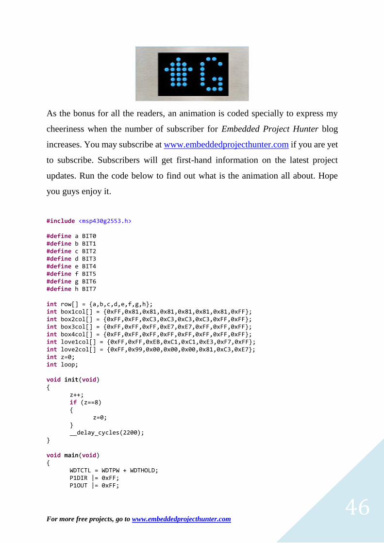
As the bonus for all the readers, an animation is coded specially to express my
cheeriness when the number of subscriber for Embedded Project Hunter blog
increases. You may subscribe at www.embeddedprojecthunter.com if you are yet
to subscribe. Subscribers will get first-hand information on the latest project
updates. Run the code below to find out what is the animation all about. Hope
you guys enjoy it.
#include <msp430g2553.h> #define a BIT0 #define b BIT1 #define c BIT2 #define d BIT3 #define e BIT4 #define f BIT5 #define g BIT6 #define h BIT7 int row[] = a,b,c,d,e,f,g,h; int box1col[] = 0xFF,0x81,0x81,0x81,0x81,0x81,0x81,0xFF; int box2col[] = 0xFF,0xFF,0xC3,0xC3,0xC3,0xC3,0xFF,0xFF; int box3col[] = 0xFF,0xFF,0xFF,0xE7,0xE7,0xFF,0xFF,0xFF; int box4col[] = 0xFF,0xFF,0xFF,0xFF,0xFF,0xFF,0xFF,0xFF; int love1col[] = 0xFF,0xFF,0xEB,0xC1,0xC1,0xE3,0xF7,0xFF; int love2col[] = 0xFF,0x99,0x00,0x00,0x00,0x81,0xC3,0xE7; int z=0; int loop; void init(void) z++; if (z==8) z=0; __delay_cycles(2200); void main(void) WDTCTL = WDTPW + WDTHOLD; P1DIR |= 0xFF; P1OUT |= 0xFF;
For more free projects, go to www.embeddedprojecthunter.com 47
P2SEL &= ~(g+h); P2DIR |= 0xFF; P2OUT |= 0xFF; while(1) P1OUT = 0xFF; P2OUT = 0; __delay_cycles(220000); for(loop=0;loop<200;loop++) P1OUT = row[z]; P2OUT = box1col[z]; init(); for(loop=0;loop<200;loop++) P1OUT = row[z]; P2OUT = box2col[z]; init(); for(loop=0;loop<200;loop++) P1OUT = row[z]; P2OUT = box3col[z]; init(); for(loop=0;loop<200;loop++) P1OUT = row[z]; P2OUT = box4col[z]; init(); for(loop=0;loop<200;loop++) P1OUT = row[z]; P2OUT = love1col[z]; init(); for(loop=0;loop<300;loop++) P1OUT = row[z]; P2OUT = love2col[z]; init();

For more free projects, go to www.embeddedprojecthunter.com 48
2.4 Liquid Crystal Display (LCD) 1. Ground
2. VCC (+3.3 to +5V)
3. Contrast adjustment (sweeper of 10k
potentiometer with opposing contacts connected to
VCC and GND respectively)
4. Register Select (RS). ->MSP430 P2.5
5. Read/~Write (R/W). ->GND
6. Clock (Enable). ->MSP430 P2.4
7. Data 0 (N.C.)
8. Data 1 (N.C.)
9. Data 2 (N.C.)
10. Data 3 (N.C.)
11. Data 4 -> MSP430 P2.0
12. Data 5 -> MSP430 P2.1
13. Data 6 -> MSP430 P2.2
14. Data 7 -> MSP430 P2.3
15. Backlight Anode (+) -> 100Ω resistor to VCC
16. Backlight Cathode (-) -> GND

For more free projects, go to www.embeddedprojecthunter.com 49
It has two type of register inbuilt that is Command Register and Data Register.
Two types of operation: 8-bit or 4-bit. The difference between 4 bit and 8 bit
operation is that data is sent out as nibbles instead of as one byte. The most
significant nibble should be transferred first, followed by the least significant
nibble.
The programming codes for LCD might be tedious as it involves two registers -
command register and data register. Fortunately, there is a LCD library well-
written by Elliott Gurrola and Luis Carlos Bañuelos-Chacon. For more
information and downloading the library, click here.
The LCD library consists of TWO files:
(i) lcdLib.h
(ii) lcdLib.c
Copy both file that you downloaded (Do not need to open the file) and then right-
click Paste in the project directory as shown below:
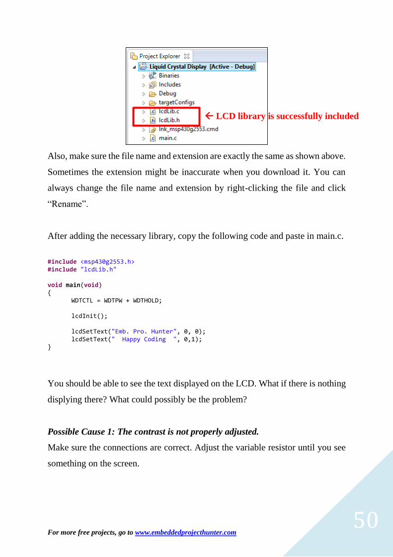
Make sure that both files are pasted successfully in the project folder. Once
successful, you should observe the following:
For more free projects, go to www.embeddedprojecthunter.com 50
Also, make sure the file name and extension are exactly the same as shown above.
Sometimes the extension might be inaccurate when you download it. You can
always change the file name and extension by right-clicking the file and click
“Rename”.
After adding the necessary library, copy the following code and paste in main.c.
#include <msp430g2553.h> #include "lcdLib.h" void main(void) WDTCTL = WDTPW + WDTHOLD; lcdInit(); lcdSetText("Emb. Pro. Hunter", 0, 0); lcdSetText(" Happy Coding ", 0,1);
You should be able to see the text displayed on the LCD. What if there is nothing
displying there? What could possibly be the problem?
Possible Cause 1: The contrast is not properly adjusted.
Make sure the connections are correct. Adjust the variable resistor until you see
something on the screen.
LCD library is successfully included
For more free projects, go to www.embeddedprojecthunter.com 51
Possible Cause 2: Voltage incompatibility
Some LCD need 5V to operate. It depends on the component you bought. If there
is nothing being display, then most probably your LCD is not 3.6V compatible.
Bear in mind that the Vcc of the microcontroller is 3.6 V.
If this is the case, you have three choices:
(i) Buy another LCD that can operate at 3.6V
(ii) Add an additional 5V power supply for the LCD
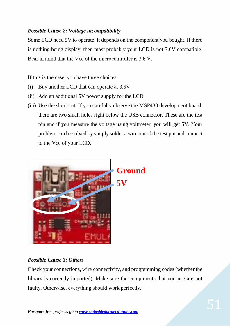
(iii) Use the short-cut. If you carefully observe the MSP430 development board,
there are two small holes right below the USB connector. These are the test
pin and if you measure the voltage using voltmeter, you will get 5V. Your
problem can be solved by simply solder a wire out of the test pin and connect
to the Vcc of your LCD.
Possible Cause 3: Others
Check your connections, wire connectivity, and programming codes (whether the
library is correctly imported). Make sure the components that you use are not
faulty. Otherwise, everything should work perfectly.
5V
Ground

For more free projects, go to www.embeddedprojecthunter.com 52
Final Thought
Yes… you have reach the last page of this e-book. Congratulation that you have
completed the tutorials. To summarize everything, you have learned:
(i) Simple LED programming
(ii) Button programming (both polling and interrupt method)
(iii) Theory on pull-up/down resistor
(iv) Working principle of button (input)
(v) Basic MSP430G2553 coding syntax
(vi) Seven-Segment Display (single and multiple)
(vii) Theory on Persistence of Vision (POV)
(viii) RGB LED
(ix) Dot Matrix LED Grid
(x) Liquid Crystal Display (LCD)
Yet, there are so much more topics to be covered, such as Analog-to-Digital
Converter (ADC), Pulse Width Modulation (PWM), and Timer. To make things
more interesting, wireless communication will be added into the list too, which
includes, Infrared (IR) line-of-sight (LOS) communication, Bluetooth
communication, Radio Frequency (RF) communication, and WiFi. Theory of
web-server and client will be discussed, together with HyperText Markup
Language (HTML) tutorials. On top of everything, you will have full control of
your WiFi-enabled devices anywhere and anytime. These topic will be covered
in Embedded Project Hunter e-book Part 2. So, stay tune!
Subscribe to Embedded Project Hunter blog to get latest updates on the new
projects. If you have any questions or thoughts, feel free to email me at
[email protected]. Hope you enjoy reading this e-book and
good luck with all your projects.

For more free projects, go to www.embeddedprojecthunter.com 53