Understanding MSP430 Flash Data · PDF fileSLAA392 2 Understanding MSP430 Flash Data Retention...
12
Application Report SLAA392 – March 2008 1 Understanding MSP430 Flash Data Retention Kripasagar Venkat, Uwe Haensel MSP430 Applications ABSTRACT The MSP430 family of microcontrollers, as part of its broad portfolio, offers both read-only memory (ROM)-based and flash-based devices. Understanding the MSP430 flash is extremely important for efficient, robust, and reliable system design. Data retention is one of the key aspects to flash reliability. In this application report, data retention for the MSP430 flash is discussed in detail and the effect of temperature is given primary importance. The concepts discussed in this document are applicable to all MSP430 devices that are flash based (F version), in any memory configuration. 1 Introduction Memory in general is broadly classified as read-only memory (ROM) or random-access memory (RAM). These two types behave differently, and each has its own set of merits and demerits. Flash memory is a hybrid of ROM and RAM, inheriting the best features of both types of memories. Flash memory, driven by low cost, is electrically programmable, fast to read from, exhibits high density, and is nonvolatile. Flash memory is usually stacked as sectors and can be erased only as sectors. For the MSP430 devices, each sector of the main memory flash is 512 bytes in length. Because the flash memory is electrically programmable, it requires a sufficient voltage to erase and program efficiently. This voltage must be maintained during the entire flash erase/write to ensure reliability of the operation. This topic is discussed in detail in the following section. The other limitation of flash is the number of writes/erases, which has a direct impact on flash wear out. Tips to ensure flash longevity and factors that contribute to flash failure are discussed in this application report. Data retention can be one of the primary concerns at extreme temperatures. In this application report, emphasis is given to basics of flash data retention, factors that influence this parameter, and the various figures of merit to interpret flash data retention, along with tips to prevent failures on the MSP430.
Transcript of Understanding MSP430 Flash Data · PDF fileSLAA392 2 Understanding MSP430 Flash Data Retention...
Application Report SLAA392 – March 2008
1
Understanding MSP430 Flash Data Retention Kripasagar Venkat, Uwe Haensel MSP430 Applications
ABSTRACT
The MSP430 family of microcontrollers, as part of its broad portfolio, offers both read-only memory (ROM)-based and flash-based devices. Understanding the MSP430 flash is extremely important for efficient, robust, and reliable system design. Data retention is one of the key aspects to flash reliability. In this application report, data retention for the MSP430 flash is discussed in detail and the effect of temperature is given primary importance. The concepts discussed in this document are applicable to all MSP430 devices that are flash based (F version), in any memory configuration.
1 Introduction
Memory in general is broadly classified as read-only memory (ROM) or random-access memory (RAM). These two types behave differently, and each has its own set of merits and demerits. Flash memory is a hybrid of ROM and RAM, inheriting the best features of both types of memories. Flash memory, driven by low cost, is electrically programmable, fast to read from, exhibits high density, and is nonvolatile. Flash memory is usually stacked as sectors and can be erased only as sectors. For the MSP430 devices, each sector of the main memory flash is 512 bytes in length. Because the flash memory is electrically programmable, it requires a sufficient voltage to erase and program efficiently. This voltage must be maintained during the entire flash erase/write to ensure reliability of the operation. This topic is discussed in detail in the following section. The other limitation of flash is the number of writes/erases, which has a direct impact on flash wear out. Tips to ensure flash longevity and factors that contribute to flash failure are discussed in this application report.
Data retention can be one of the primary concerns at extreme temperatures. In this application report, emphasis is given to basics of flash data retention, factors that influence this parameter, and the various figures of merit to interpret flash data retention, along with tips to prevent failures on the MSP430.

SLAA392
2 Understanding MSP430 Flash Data Retention
2 MSP430 Flash Characteristics
The thick-oxide split-gate cell design used in the MSP430 has several advantages in terms of data retention and endurance performance compared to other flash cell architectures such as thin-oxide stacked-gate or thin-oxide two-transistor cell designs. It is easier to manufacture and less susceptible than thin-oxide designs to manufacturing defects that relate to data retention loss over time.
2.1 Flash Programming
The erase state of every bit in any location in the MSP430 flash is logic 1. It is important and recommended that the user perform an erase operation before writing/programming is done to any location in MSP430 flash. Most of the MSP430 devices shipped from the factory have their main memory completely erased, while information memory might contain factory test data.
2.1.1 Programming Tips
In this section, a few external and internal tips that should be followed to minimize adverse effects during system design are listed. Failure to adhere to any of these tips may result in unreliable flash write/erase, leading to unpredictable flash behavior.
Internal Considerations
Efficient programming of the MSP430 flash is governed by two major requirements: supply voltage (DVCC) and the flash timing generator clock (fFTG). For the MSP430F1xx and most of the MSP430F4xx family of devices, the supply voltage must be a minimum of 2.7 V. The minimum supply voltage is reduced to 2.2 V and 1.8 V for the MSP430F2xx family and MSP430F5xx families, respectively. Particularly in battery-powered applications, battery capacity must be sufficient to meet the minimum operating voltage and currents necessary for in-application program/erase. The fFTG for MSP430F1xx, MSP430F2xx, and MSP430F4xx devices must be in the range of 257 kHz ≤ fFTG ≤ 476 kHz, while it is generated internally on the MSP430F5xx devices. There is a practical limit on the number of flash erase/write cycles for every MSP430, which is in the range of 100,000 cycles.
External Considerations
Use of a programming adapter that has been certified to meet the MSP430 flash programming specifications greatly reduces the risk of a flash failure. Regular inspection for wear out of the programming socket also ensures better performance over time. If in-circuit programming is done via JTAG or boot loader, the programming operation should be performed at the end of the manufacturing cycle. Mechanical and thermal process steps, such as encapsulation mold cure, should be completed before programming.
Verification is an important step that can be implemented, if flash integrity must be checked. A checksum routine can be called on a regular basis for critical applications. In some of the MSP430F2xx, MSP430F4xx, and MSP430F5xx devices, the Marginal Read Mode is implemented to facilitate a checksum routine. Checksum routine values with and without this feature are compared to find weak programming flash locations on the MSP430. Different values may indicate a violation of one or more of the above mentioned programming considerations.

SLAA392
Understanding MSP430 Flash Data Retention 3
2.2 Flash Failure Mechanism
This section describes a few intrinsic and extrinsic failure mechanisms of flash memory. Although these mechanisms are applicable to any industry flash, they apply to the MSP430 flash as well. Several tests are in place to ensure that each MSP430 that leaves the factory does not show any of the following symptoms.
Charge Retention
Charge retention is the ability of the flash cell to retain its programmed value during long-term storage. If there are defects in the dielectrics or the substrate, charges can move to or from the floating gate, causing elevated charge loss. Also, with sufficient thermal activation, all bits could lose their charge. Analyses indicate that this failure mechanism occurs well beyond the normal lifetime of the device. Charge retention is discussed more in Section 2.3.
Oxide Degradation
The high fields used during program and erase can result in increased low field leakage through the dielectrics of the cell. This can increase the susceptibility to charge loss of the cell. Analyses and long-term storage results have verified that the post-cycling retention performance of the cells extends well beyond normal lifetimes.
Program/Erase Time Degradation
After a large number of write/erase cycles, a high charge can be trapped in the dielectrics surrounding the floating gate. This charge can decrease the effective field across the cell during program and erase operations, increasing the time required to complete the program/erase operations. Data on TI flash cells has shown that the erase/program time walk-out is well beyond normal use conditions.
Write Disturb
During the program operation, high fields are placed not only on the bit being programmed, but on other bits along the same word line and/or bit line. If there are defects in the dielectrics or in the substrate, leakage paths can be created, so inadvertent programming of a non-selected bit can be observed. To address this defect mechanism, high-voltage screens are in place in the test program to eliminate such units from the population.
These are some of the failure mechanisms that could occur to any flash, and tests are place to for screen out any MSP430 devices that might have them.
2.3 Flash Data Retention
Data retention of any flash is the ability to retain its programmed state. Flash data retention is known to degrade over temperature. Various tests and methods are in place to determine the reliability of flash. Tthis application report mainly addresses the concept of accelerated test and the use of statistics to predict reliability.

SLAA392
4 Understanding MSP430 Flash Data Retention
2.3.1 Accelerated Tests
To test the flash data retention at various temperatures we make use of accelerated tests on the flash. These tests are wholly based on Arrhenius law and equation. The Arrhenius theory allows the test of any device under accelerated environments for short periods and predicts the behavior under normal conditions for longer periods. Similar tests are performed on the MSP430 flash to test and predict data retention. During each test, an unprogrammed device is subjected to these tests. A flash failure is indicated when any of the flash cells change from an unprogrammed state (logic 1) to logic 0. The Arrhenius equation is shown in Equation 1.
−−
= 12
aT1
T1
kE
eAF (1)
AF = Acceleration factor
Ea = Activation energy (0.6 eV for data retention)
k = Boltzmann's constant (8.623 x 10⁻⁵ eV/K)
T1 = Application junction temperature in Kelvin
T2 = Accelerated stress junction temperature in Kelvin
Depending on AF, a back calculation using the Arrhenius equation for any desired temperature leads to fairly accurate data-retention times.
Infant Mortality Test During Production
This test is not a flash data retention test, rather, it is performed to screen out infant mortality among devices during production. It is an accepted theory that all devices statistically follow a bathtub curve when it comes to failures. The infant mortality failures would fall into the left hand slope of the bath tub curve. Under this test, all of the MSP430 devices are baked for 72 hours or 144 hours at 250°C.
Flash Data Retention Tests During Qualification
To determine the flash data retention, further tests are conducted during qualification of the MSP430 devices. Two cases are explained in this section for different temperature and baking time.
Case 1: 420-Hour Baking Time at 170°C
In this test, the MSP430 is continuously subjected to this high temperature of 170°C for 420 hours. The purpose of this test is to determine data retention at higher temperatures, and then calculate expected data retention at 25°C using Equation 2.
Using T1 = 25°C and T2 = 170°C in Equation 1 gives the following AF:
2085eeAF (298)1
(443)1
108.6230.6
273)(25C1
273)(170C1
kE
5a
===
−
×−
+
−+
−−
(2)
SLAA392
Understanding MSP430 Flash Data Retention 5
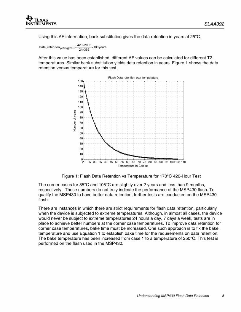
Using this AF information, back substitution gives the data retention in years at 25°C.
years100365242085420tionData_reten years@25C ≈
××
=
After this value has been established, different AF values can be calculated for different T2 temperatures. Similar back substitution yields data retention in years. Figure 1 shows the data retention versus temperature for this test.
20 25 30 35 40 45 50 55 60 65 70 75 80 85 90 95 100 105 1100
10
20
30
40
50
60
70
80
90
100
110
120
130
140
150
Temperature in Celcius
Num
ber
of y
ears
Flash Data retention over temperature
Figure 1: Flash Data Retention vs Temperature for 170°C 420-Hour Test
The corner cases for 85°C and 105°C are slightly over 2 years and less than 9 months, respectively. These numbers do not truly indicate the performance of the MSP430 flash. To qualify the MSP430 to have better data retention, further tests are conducted on the MSP430 flash.
There are instances in which there are strict requirements for flash data retention, particularly when the device is subjected to extreme temperatures. Although, in almost all cases, the device would never be subject to extreme temperatures 24 hours a day, 7 days a week, tests are in place to achieve better numbers at the corner case temperatures. To improve data retention for corner case temperatures, bake time must be increased. One such approach is to fix the bake temperature and use Equation 1 to establish bake time for the requirements on data retention. The bake temperature has been increased from case 1 to a temperature of 250°C. This test is performed on the flash used in the MSP430.
SLAA392
6 Understanding MSP430 Flash Data Retention
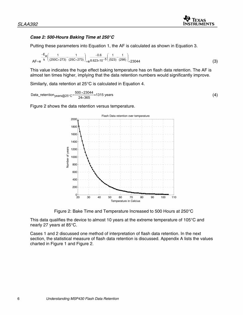
Case 2: 500-Hours Baking Time at 250°C
Putting these parameters into Equation 1, the AF is calculated as shown in Equation 3.
23044eeAF (298)1
(523)1
5108.623
0.6273)(25C
1273)(250C
1k
aE
===
−
−×
−
+
−+
−
(3)
This value indicates the huge effect baking temperature has on flash data retention. The AF is almost ten times higher, implying that the data retention numbers would significantly improve.
Similarly, data retention at 25°C is calculated in Equation 4.
years13153652423044 500tionData_reten Cyears@25 ≈××
=° (4)
Figure 2 shows the data retention versus temperature.
20 30 40 50 60 70 80 90 100 1100
200
400
600
800
1000
1200
1400
1600
1800
2000
Temperature in Celcius
Num
ber
of y
ears
Flash Data retention over temperature
Figure 2: Bake Time and Temperature Increased to 500 Hours at 250°C
This data qualifies the device to almost 10 years at the extreme temperature of 105°C and nearly 27 years at 85°C.
Cases 1 and 2 discussed one method of interpretation of flash data retention. In the next section, the statistical measure of flash data retention is discussed. Appendix A lists the values charted in Figure 1 and Figure 2.
SLAA392
Understanding MSP430 Flash Data Retention 7
2.3.2 Reliability Tests
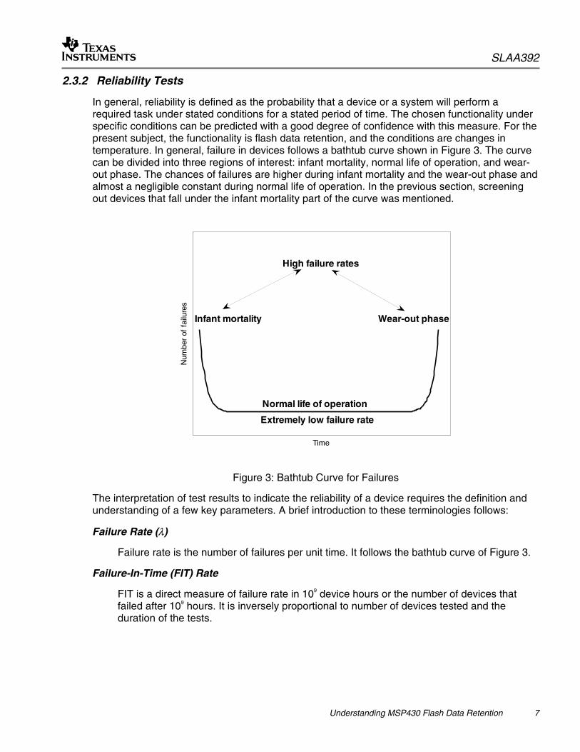
In general, reliability is defined as the probability that a device or a system will perform a required task under stated conditions for a stated period of time. The chosen functionality under specific conditions can be predicted with a good degree of confidence with this measure. For the present subject, the functionality is flash data retention, and the conditions are changes in temperature. In general, failure in devices follows a bathtub curve shown in Figure 3. The curve can be divided into three regions of interest: infant mortality, normal life of operation, and wear-out phase. The chances of failures are higher during infant mortality and the wear-out phase and almost a negligible constant during normal life of operation. In the previous section, screening out devices that fall under the infant mortality part of the curve was mentioned.
Time
Num
ber
of f
ailu
res
Infant mortality
Normal life of operation
Wear-out phase
Extremely low failure rate
High failure rates
Figure 3: Bathtub Curve for Failures
The interpretation of test results to indicate the reliability of a device requires the definition and understanding of a few key parameters. A brief introduction to these terminologies follows:
Failure Rate (λ)
Failure rate is the number of failures per unit time. It follows the bathtub curve of Figure 3.
Failure-In-Time (FIT) Rate
FIT is a direct measure of failure rate in 109 device hours or the number of devices that failed after 109 hours. It is inversely proportional to number of devices tested and the duration of the tests.

SLAA392
8 Understanding MSP430 Flash Data Retention
Acceleration Factor (AF)
AF is an outcome of an accelerated life test done on the device to predict its long-term performance. Its role in the Arrhenius equation was shown in previous sections. This factor also contributes inversely to the FIT.
Confidence Level (CL)
CL is the probability level estimated based on sample tests conducted for failures. It also is a confidence in the integrity of numbers used to determine the failure rate. It follows a chi-square (χ2) distribution and depends on the number of failures. In most cases, the confidence level is chosen to be 60% or 90%. It directly contributes to the FIT.
Mean Time Between Failures (MTBF)
MTBF is the inverse of the FIT for a repairable device and is a classic measure of reliability of a system or of a product. It is figure that goes through constant update with number of samples tested and failed.
Reliability [R(t)]
R(t) is defined for fixed time periods to predict the number of devices that would perform reliably. It is a byproduct of the FIT and expressed as a percentage.
From this point on, it is a simple task of putting these numbers in their respective formulae to get reliability data. An example is shown for the tests discussed in the previous section.
Example 1
Consider the test conducted in Case 1 for MSP430 flash with the temperature set to 170°C for a time of 420 hours. The sample size is 240 and the AF, FIT, and MTBF are shown for confidence levels of 60% and 90%.
The AF is still calculated using Equation 1 for each temperature in question:
1418eeAF (303)1
(443)1
108.6230.6
273)(30C1
273)(170C1
kE
5a
===
−
×−
+
−+
−−
H = Time for which the device is tested for in hours = 420
N = Number of devices = 240
AFHN
102χ
FIT
92
××
×
=

SLAA392
Understanding MSP430 Flash Data Retention 9
The value of χ2/2 for confidence levels of 0.6 and 0.9 from the χ2 distribution gives a value of 0.916 and 2.305 respectively. The FIT is therefore:
( ) 6.411418420240100.916
AFHN
102χ
FIT9
92
CLC,0.6300 =×××
=××
×
=
( ) 16.131418420240102.305
AFHN
102χ
FIT9
92
CLC,0.9300 =×××
=××
×
=
The FIT numbers are expressed in number of parts failing per billion units, as indicated by the 109 factor.
Once the FIT numbers are known, it is easy to calculate the MTBF defined by:
9years 10
36524FIT1MTBF ×××
=
years1780910365246.41
11036524FIT
1MTBF 99
CLC,0.630CLC,0.6years,30 0
0 =×××
=×××
=
years7077103652416.13
11036524FIT
1MTBF 99
CLC,0.930CLC,0.9years,30 0
0 =×××
=×××
=
Example 2
If the reliability for a fixed period of time needs to be calculated for a device, the following equation can be used:
t/MTBFeR(t) −=
t = Period of interest
In combination with Example 1, a problem statement can be derived to determine the reliability of a device that is constantly subjected to a single temperature for a set period of time. Suppose t is defined as 20 years and the MTBF for 30°C was used (from Example 1) with confidence levels of 0.6 and 0.9, the reliability is:
99.88%0.9988ee(t)R (20/17809)t/MTBFCLC,0.630 ==== −−
°
99.71%0.9971ee(t)R (20/7077)t/MTBFCLC,0.930 ==== −−
°
These results indicate the reliability of the MSP430 flash data retention devices at a fixed temperature and time. If Case 2 results were used in Example 1 and Example 2, the numbers obtained for MTBF and reliability would be even better.

SLAA392
10 Understanding MSP430 Flash Data Retention
3 Conclusion
This application report has addressed the means to understand data retention for the MSP430 flash. Various tests performed on the MSP430 that truly reflected flash data retention in number of years were described. Statistical measures were introduced to understand the MSP430 performance. Examples showed how MTBF numbers can be used to calculate reliability of an MSP430 under various conditions influenced by temperature.

SLAA392
Understanding MSP430 Flash Data Retention 11
Appendix A. Tabular Results
Case 1 Results Temperature
(°C) Data Retention
(Years)
20 148.912
25 100.000
30 68.006
35 46.843
40 32.652
45 23.020
50 16.406
55 11.814
60 8.591
65 6.307
70 4.672
75 3.491
80 2.630
85 1.997
90 1.528
95 1.178
100 0.914
105 0.714
Case 2 Results Temperature
(°C) Data Retention
(Years) 20 1959.187
25 1315.313
30 894.733
35 616.298
40 429.597
45 302.872
50 215.853
55 155.432
60 113.033
65 82.979
70 61.466
75 45.926
80 34.599
85 26.272
90 20.102
95 15.493
100 12.024
105 9.395

IMPORTANT NOTICETexas Instruments Incorporated and its subsidiaries (TI) reserve the right to make corrections, modifications, enhancements, improvements,and other changes to its products and services at any time and to discontinue any product or service without notice. Customers shouldobtain the latest relevant information before placing orders and should verify that such information is current and complete. All products aresold subject to TI’s terms and conditions of sale supplied at the time of order acknowledgment.TI warrants performance of its hardware products to the specifications applicable at the time of sale in accordance with TI’s standardwarranty. Testing and other quality control techniques are used to the extent TI deems necessary to support this warranty. Except wheremandated by government requirements, testing of all parameters of each product is not necessarily performed.TI assumes no liability for applications assistance or customer product design. Customers are responsible for their products andapplications using TI components. To minimize the risks associated with customer products and applications, customers should provideadequate design and operating safeguards.TI does not warrant or represent that any license, either express or implied, is granted under any TI patent right, copyright, mask work right,or other TI intellectual property right relating to any combination, machine, or process in which TI products or services are used. Informationpublished by TI regarding third-party products or services does not constitute a license from TI to use such products or services or awarranty or endorsement thereof. Use of such information may require a license from a third party under the patents or other intellectualproperty of the third party, or a license from TI under the patents or other intellectual property of TI.Reproduction of TI information in TI data books or data sheets is permissible only if reproduction is without alteration and is accompaniedby all associated warranties, conditions, limitations, and notices. Reproduction of this information with alteration is an unfair and deceptivebusiness practice. TI is not responsible or liable for such altered documentation. Information of third parties may be subject to additionalrestrictions.Resale of TI products or services with statements different from or beyond the parameters stated by TI for that product or service voids allexpress and any implied warranties for the associated TI product or service and is an unfair and deceptive business practice. TI is notresponsible or liable for any such statements.TI products are not authorized for use in safety-critical applications (such as life support) where a failure of the TI product would reasonablybe expected to cause severe personal injury or death, unless officers of the parties have executed an agreement specifically governingsuch use. Buyers represent that they have all necessary expertise in the safety and regulatory ramifications of their applications, andacknowledge and agree that they are solely responsible for all legal, regulatory and safety-related requirements concerning their productsand any use of TI products in such safety-critical applications, notwithstanding any applications-related information or support that may beprovided by TI. Further, Buyers must fully indemnify TI and its representatives against any damages arising out of the use of TI products insuch safety-critical applications.TI products are neither designed nor intended for use in military/aerospace applications or environments unless the TI products arespecifically designated by TI as military-grade or "enhanced plastic." Only products designated by TI as military-grade meet militaryspecifications. Buyers acknowledge and agree that any such use of TI products which TI has not designated as military-grade is solely atthe Buyer's risk, and that they are solely responsible for compliance with all legal and regulatory requirements in connection with such use.TI products are neither designed nor intended for use in automotive applications or environments unless the specific TI products aredesignated by TI as compliant with ISO/TS 16949 requirements. Buyers acknowledge and agree that, if they use any non-designatedproducts in automotive applications, TI will not be responsible for any failure to meet such requirements.Following are URLs where you can obtain information on other Texas Instruments products and application solutions:Products ApplicationsAmplifiers amplifier.ti.com Audio www.ti.com/audioData Converters dataconverter.ti.com Automotive www.ti.com/automotiveDSP dsp.ti.com Broadband www.ti.com/broadbandClocks and Timers www.ti.com/clocks Digital Control www.ti.com/digitalcontrolInterface interface.ti.com Medical www.ti.com/medicalLogic logic.ti.com Military www.ti.com/militaryPower Mgmt power.ti.com Optical Networking www.ti.com/opticalnetworkMicrocontrollers microcontroller.ti.com Security www.ti.com/securityRFID www.ti-rfid.com Telephony www.ti.com/telephonyRF/IF and ZigBee® Solutions www.ti.com/lprf Video & Imaging www.ti.com/video
Wireless www.ti.com/wireless
Mailing Address: Texas Instruments, Post Office Box 655303, Dallas, Texas 75265Copyright © 2008, Texas Instruments Incorporated