Ethesis Naeem Public Ed 3kth.diva-portal.org/smash/get/diva2:548469/FULLTEXT01.pdf · 3.1 Mass...
76
KTH ROYAL INSTITUTE OF TECHNOLOGY Technology and properties of InP-based photonic crystal structures and devices Naeem Shahid Division of Semiconductor Materials KTH School of Information and Communication Technology Doctoral Thesis Stockholm, Sweden 2012
Transcript of Ethesis Naeem Public Ed 3kth.diva-portal.org/smash/get/diva2:548469/FULLTEXT01.pdf · 3.1 Mass...

KTH ROYAL INSTITUTE OF TECHNOLOGY
Technology and properties of
InP-based photonic crystal structures and devices
Naeem Shahid
Division of Semiconductor Materials KTH School of Information and Communication Technology
Doctoral Thesis Stockholm, Sweden 2012

TECHNOLOGY AND PROPERTIES OF INP-BASED PHOTONIC CRYSTAL
STRUCTURES AND DEVICES
TRITA-ICT/MAP AVH Report 2012:14 ISSN 1653-7610 ISRN KTH/ICT-MAP/AVH-2012:14-SE ISBN 978-91-7501-442-5
KTH School of Information and Communication Technology
SE-164 40 KistaSWEDEN
Akademisk avhandling som med tillstånd av Kungl Tekniska Högskolan framlägges till offentlig granskning för avläggande av teknologie doktorsexamen i fotonik, torsdagen den 17 september 2012 kl 10:00 i sal C2, Electrum 229, Kungl Tekniska Högskolan, Isafjordsgatan 22-26, 16432 Kista, Stockholm. ©Naeem Shahid, August 2012 Tryck: Universitetsservice US AB
Cover Picture: A photonic crystal waveguide with 3 missing row (W3). Top XY-plane is the SEM image of fabricated waveguide. Finite difference (FD) simulated mode distribution of TE mode is shown in left YZ-plane.

iii
TABLEOFCONTENTS
Abstract ....................................................................................................................................... v
Acknowledgements ................................................................................................................... vi
List of papers........................................................................................................................... viii
List of Appended papers: ........................................................................................................ viii
Related contributions not included in the thesis: ...................................................................... ix
Acronyms and Notations........................................................................................................... xi
Chapter 1 Introduction ................................................................................................................ 1
1.1 Properties of 2D Photonic crystals (PhCs) ....................................................................... 4
1.1.1 Light propagation in PhCs ........................................................................................ 4
1.1.2 The 2D PhC lattice .................................................................................................... 6
1.1.3 Light propagation in 2D PhCs .................................................................................. 6
1.1.4 Plane Wave Expansion (PWE) method .................................................................... 7
1.1.5 The Band structure .................................................................................................... 7
1.1.6 InGaAsP/InP material system ................................................................................... 8
1.2 Outline of this thesis ....................................................................................................... 10
Chapter 2 Fabrication Technology ............................................................................................ 11
2.1 Low vertical contrast InP-based material system (Substrate-type) ................................ 12
2.1.1 Plasma-enhanced chemical vapor deposition (PECVD) of the hard mask ............. 12
2.1.2 Electron beam lithography ...................................................................................... 13
2.1.3 Reactive ion etching (RIE) of a hard mask ............................................................. 14
2.1.4 Chemically assisted ion beam etching of substrate-type PhCs ............................... 16
2.1.5 Scanning Electron Microscopy (SEM) analysis of Fabricated Samples ................ 19
2.2 High vertical contrast InP-based material system (Membrane-type) ............................. 21
2.2.1 Inductively coupled plasma based RIE for fabrication of membrane ..................... 21
2.2.2 Selective wet etching to fabricate PhC membrane ................................................. 24
2.3 Active layer structure for InGaAsP membrane .............................................................. 25
2.3.1 Micro-photoluminescence (μ-PL) spectroscopy of PhC membranes ..................... 26
2.3.2 Hexagonal defect H2 cavity in PhC membrane ...................................................... 27
Chapter 3 Mass Transport on InP Photonic Crystals ................................................................ 30
3.1 Mass Transport (MT) process ........................................................................................ 30
3.2 Redistribution of InP by mass transport ......................................................................... 31
3.3 Annealing of InP-based photonic crystals ...................................................................... 32
3.3.1 Annealing under Phosphine (PH3) atmosphere ....................................................... 32
3.3.2 Annealing under Arsine (AsH3) atmosphere .......................................................... 33

iv
Chapter 4 Photonic Crystal Device Applications ..................................................................... 35
4.1 End-fire characterization ................................................................................................ 35
4.2 Multimode interference coupler (MMI) with internal PhC ............................................ 37
4.3 Photonic crystal waveguides (PCWs) ............................................................................ 38
4.4 Contra-directional coupling in PhC waveguides ............................................................ 39
4.5 Transmission through W3 guides ................................................................................... 40
4.6 Wideband Optical filtering ............................................................................................. 41
4.7 Ultrasharp band-edge ..................................................................................................... 42
4.8 Structural tuning ............................................................................................................. 43
4.8.1 Air fill factor ........................................................................................................... 43
4.8.2 Hole-widening due to proximity effect ................................................................... 44
4.8.3 Waveguide line-defect width .................................................................................. 45
4.9 Heterostructure PhC waveguiudes ................................................................................. 46
4.9.1 Junction-type PhC waveguides (JPCW) ................................................................. 46
4.9.2 Heterostructure W3 (HW3) PhC waveguide .......................................................... 47
4.10 Temperature tuning of photonic crystal waveguides .................................................. 49
4.11 Reliability of PhC waveguides ................................................................................... 50
Chapter 5 Conclusions and outlook .......................................................................................... 52
5.1 Fabrication of PhC structures ......................................................................................... 52
5.2 Device applications of PhCs .......................................................................................... 53
Chapter 6 Guide to the papers ................................................................................................... 55
Bibliography ............................................................................................................................. 58

v
ABSTRACT
Photonic crystals (PhCs) are periodic dielectric structures that exhibit a photonic band gap; a range of wavelengths for which light propagation is forbidden. 2D PhCs exhibit most of the properties as their three dimension counterparts with a compatibility with standard semiconductor processing techniques such as epitaxial growth, electron beam lithography, Plasma deposition/etching and electromechanical lapping/polishing. Indium Phosphide (InP) is the material of choice for photonic devices especially when it comes to realization of coherent light source at 1.55 μm wavelength. Precise engineering of the nanostructures in the PhC lattice offers novel ways to confine, guide and control light in phonic integrated circuits (PICs). Strong confinement of light in PhCs offer novel opportunities in many areas of physics and engineering.
Dry etching, a necessary process step in PhC device manufacturing, is known to introduce damage in the etched material. Process induced damage and its impact on the electrical and optical properties of PhCs depends on the etched material, the etching technique and process parameters. We have demonstrated a novel post-etch process based on so-called mass-transport (MT) technology for the first time on InP-based PhCs that has significantly improved side-wall verticality of etched PhC holes. A statistical analysis performed on several devices fabricated by MT process technology shows a great deal of improvement in the reliability of optical transmission characteristics which is very promising for achieving high optical quality in PhC components. Several PhC devices were manufactured using MT technology.
Broad enough PhC waveguides that operate in the mono/multi-mode regime are interesting for coarse wavelength de-multiplexing. The fundamental mode and higher order mode interaction creates mini-stop band (MSB) in the dispersion diagram where the higher order mode has a lower group velocity which can be considered as slow light regime. In this thesis work, the phenomena of MSBs and its impact on transmission properties have been evaluated. We have proposed and demonstrated a method that enables spectral tuning with sub-nanometer accuracy which is based on the transmission MSB. Along the same lines most of the thesis work relates to broad enough PhC guides that operated in the multimode regime. Temperature tuning experiments on these waveguides reveals a clear red-shift with a gradient of dλ/dT=0.1 nm/˚C. MSBs in these waveguides have been studied by varying the width in incremental amounts.
Analogous to semiconductors heterostructures, photonic heterostructures are composed of two photonic crystals with different band-gaps obtained either by changing the air-fill factor or by the lattice constant. Juxtaposing two PhC and the use of heterostructures in waveguide geometry has been experimentally investigated in this thesis work. In particular, in multimode line defect waveguides the “internal” MSB effect brings a new dimension in single junction-type photonic crystal waveguide (JPCW) and heterostructure W3 (HW3) for fundamental physics and applications. We have also fabricated an ultra-compact polarization beam splitter (PBS) realized by combining a multimode waveguide with internal PhC. MSBs in heterostructure waveguides have shown interesting applications such as designable band-pass flat-top filters, and resonance-like filters with high transmission.
In the course of this work, InGaAsP suspended membrane technology was developed. An H2 cavity with a linewidth of ~0.4 nm, corresponding to a Q value of ~3675 has been shown. InGaAsP PhC membrane is an ideal platform to study coupled quantum well/dot-nanocavity system.
Keywords: Integrated optics materials; Photonic crystals; Planar waveguides; Dispersion; Band-gap; Mode-gap; mini-stopband, InP, Nanostructure fabrication; dry etching; mass transport; material reflow; reliability.

vi
ACKNOWLEDGEMENTS
Foremost, I would like to express my sincere gratitude to my supervisor, Srinivasan Anand, for giving me the confidence to undertake new research problems and keeping an eye on my progress for the past 4.5 years. I gratefully thank him for his guidance, understanding, and continuous support of the research during my graduate studies at KTH. I would also like to express my greatest appreciation to our group head, Prof. Sebastian Lourdudoss, for his remarkable goodwill with all aspects of this process. I am extremely thankful for the time, help, motivation and facilities they both have provided to me. Besides, I would like to thank the authority of KTH for providing a good environment, excellent facilities and a partial financial support to complete this PhD project. I would also like to convey thanks to the HEC, Pakistan for giving me an opportunity to do my PhD in Sweden and providing me with major part of the financial means to complete this task. The experimental research activities were mainly funded by Swedish Strategic Research Foundation (SSF) and Swedish Research Council (VR).
I am very grateful to many colleagues I had the pleasure to work with: Audrey Berrier for training me on CAIBE and other cleanroom processes, Mingyu Li for helping me to understand the basic concepts of integrated optics, Shagufta Naureen for helping me with scanning electron microscopy and wet chemical processes. I thank Reza Sanatinia, Muhammad Amin, Noud Speijcken, Bikash Dev Choudhery, Perumal Rajagembu, Murthy O V S N and Kashif Masud Awan for friendly discussions. I am also thankful to the bigger HMA group members; Carl Junesand, Wondwosen Mataferia, Himanshu Kataria, Yanting Sun, Ming Hong Gau, Thomas Aggerstam, Fredrik Olsson, Mony Nagarajan, Pritesh Dagur and Chen Hu for sharing their research activities. I have learned a lot from all these talented researchers by working in a team environment. I sincerely thank Marianne Widing and Medeleine Prinzsköld for an efficient administrative support.
I am thankful to Terrance Burks for reading this thesis and native speaker’s advice on the English language.
I would also like to express my appreciation to the following Lab. colleagues:
Prof. David Haviland, Anders Liljeborg and Anders Holmberg for providing access, support and advice for electron beam lithography. Yaocheng Shi for training me on this Raith-150 electron beam lithography system.
Marcin Swillo for helping me with optical transmission experiments. Lech Wosinski for providing access to optical characterization lab.
Prof. Mattias Hammar and Jesper Berggren for providing high quality epitaxy. Sven Valerio, Reza Nikpars, Aleksandar Radojcic, Per Wehlin and Magnus Lindberg for being instrumental in smooth running of cleanroom processes.
An honourable mention goes to my friends for their support to the entire family during the way through the ups and downs all through this journey: Himanshu Kataria, Hanna Samuelsson, Terrance Burks, Mohsin Saleemi, Henry Radamson, Apurba Dev, Anurupa Dev. Without helps of these particular, we would face many difficulties while doing this. Also, I thank to Muhammad Usman, Benedetto Buono, Anna Lopez Cabezas, Marta Avila Perez, Sofia Triana, Robina Saeed Khan, Shahid Hussain, Mazher Ahmed Yar, Umer Shah, Xiaoyue Wu and A. B. M. Hamidul Islam for a warm company.

vii
Finally, and most importantly, I wish to express love and gratitude to my beloved family, Shagufta, Muhammad and Zain, for their understanding, patience, endless love and inspiring support. I thank my parents, Javaid and Perveen, for their faith in me and allowing me to be as ambitious as I wanted. It was under their watchful eye that I gained so much drive and an ability to tackle challenges.
Naeem Shahid Stockholm Aug. 2012

viii
LISTOFPAPERS
List of Appended papers:
Paper A N. Shahid, S. Naureen, M. Y. Li, M. Swillo, and S. Anand, “Novel postetch process to realize high quality photonic crystals in InP,” J. Vac. Sci. Technol. B 29, 031202 (2011).
Paper B
Y. Shi, N. Shahid, M. Y. Li, A. Berrier, S. He, and S. Anand, “Experimental demonstration of an ultracompact polarization beamsplitter based on a multimode interference coupler with internal photonic crystals,” Optical Engineering 49, 060503 (2010).
Paper C
Naeem Shahid, Shagufta Naureen, Ming-Yu Li, Marcin Swillo, and Srinivasan Anand, “High quality photonic crystal waveguide filters based on mode-gap effect,” 23rd International Conference on Indium Phosphide and Related Materials Berlin, Germany – IPRM, ISBN: 978-3-8007-3356-9 (2011).
Paper D N. Shahid, N. Speijcken, S. Naureen, M. Y. Li, M. Swillo, and S. Anand, “Ultrasharp ministop-band edge for subnanometer tuning resolution,” Appl. Phys. Lett. 98, 0811121 (2011).
Paper E N. Shahid, M. Amin, S. Naureen, M. Swillo, and S. Anand, “Junction-type photonic crystal waveguides for notch- and pass-band filtering,” Opt. Express Vol. 19, No. 21, 21074 (2011).
Paper F N. Shahid, M. Amin, S. Naureen, and S. Anand, “Mini-stop bands in single heterojunction photonic crystal waveguides,” Submitted to Appl. Phys. Lett. (2012).
Paper G Naeem Shahid, Shagufta Naureen, and Srinivasan Anand, “Effect of hole shapes on the reliability of deeply-etched InP-based photonic crystal devices,” Phys. Status Solidi C 9, No. 7, 1670–1673 (2012).

ix
Related contributions not included in the thesis:
Articles:
1. M. Y. Li, S. Naureen, N. Shahid, and S. Anand, “Fabrication of Submicrometer InP Pillars by Colloidal Lithography and Dry Etching,” J. Electrochem. Soc. 157, H896 (2010).
2. S. Naureen, R. Sanatinia, N. Shahid, and S. Anand, “High Optical Quality InP-Based Nanopillars Fabricated by a Top-Down Approach,” Nano Lett. 11(11), 4805–4811 (2011).
3. N. Shahid, M. Li, S. Naureen, M. Swillo, and S. Anand, “Engineering mode-gaps on photonic crystal waveguides for filtering applications,” CLEO/Europe and EQEC 2011 Conference Digest, OSA Technical Digest, Optical Society of America, DOI: 10.1109/CLEOE.2011.5942825 (2011).
4. S. Anand, N. Shahid, M. Swillo, “InP-Based photonic crystal waveguide technology for filtering and sensing applications,” 13th International Conference on Transparent Optical Networks (ICTON), DOI: 10.1109/ICTON.2011.5970998 (2011).
5. Shagufta Naureen, Perumal Rajagembu, Reza Sanatinia, Naeem Shahid, Mingyu Li, and Srinivasan Anand, “Nanostructuring of InP by colloidal lithography and ICP etching for photovoltaic applications,” 23rd International Conference on Indium Phosphide and Related Materials Berlin, Germany– IPRM (2011).
Conferencecontributions:
1. Naeem Shahid*, Shagufta Naureen, and Srinivasan Anand, “Effect of hole shapes on the reliability of deeply-etched InP-based photonic crystal devices,” 16th Semiconducting and Insulating Materials Conference (SIMC-XVI), Jun. 19-23, 2011, Stockholm, Sweden.
2. S. Naureen*, R. Sanatinia, B. Choudhury, N. Shahid, R. Perumal and S. Anand, “Nanopattering of semiconductors using self-assembled silicon-di-oxide nanospheres as etch masks,” 16th Semiconducting and Insulating Materials Conference (SIMC-XVI), Jun. 19-23, 2011, Stockholm, Sweden.
3. Naeem Shahid*, Ming-Yu Li, Shagufta Naureen, Marcin Swillo, and Srinivasan Anand, “Engineering mode-gaps on photonic crystal waveguides for filtering applications,” The European Conference on Lasers and Electro-Optics (CLEO/Europe), May 22–26, 2011, Munich, Germany.
4. Naeem Shahid*, Shagufta Naureen, Ming-Yu Li, Marcin Swillo, and Srinivasan Anand, “High quality photonic crystal waveguide filters based on mode-gap effect,” 23rd International Conference on Indium Phosphide and Related Materials (IPRM), May 22–26, 2011, Berlin, Germany.
5. Shagufta Naureen*, Perumal Rajagembu, Reza Sanatinia, Naeem Shahid, Mingyu Li, and Srinivasan Anand, “Nanostructuring of InP by colloidal lithography and ICP etching for photovoltaic applications,” 23rd International Conference on Indium Phosphide and Related Materials (IPRM), May 22–26, 2011, Berlin, Germany.
6. Naeem Shahid*, Shagufta Naureen, Ming-Yu Li, Marcin Swillo, and Srinivasan Anand, “Reshaping high-aspect ratio nanostructures in InP by material reflow,” E-MRS 2011 Spring Meeting, May 9-13, 2011, Nice, France.

x
7. P. Rajagembu*, S. Naureen*, N. Shahid, R. Sanatinia and S. Anand, “Fabrication of Indium Phosphide nanopillars by nanosphere lithography and dry etching,” E-MRS 2011 Spring Meeting, May 9-13, 2011, Nice, France.
8. S. Anand*, N. Shahid, M. Swillo, InP-based photonic crystal waveguide technology for filtering and sensing applications, 13th International Conference on Transparent Optical Networks (ICTON), Jun. 26-30, 2011, Stockholm, Sweden.
9. S. Anand*, N. Shahid, S. Naureen, M-Y. Li and M. Swillo, “InP-based photonic crystal waveguide filters”, Asia communications and photonics conference (ACP 2010), Dec. 8-12, 2010, Shangai, China.
10. N. Shahid*, M. Amin, N. Speijcken, S. Naureen, M. Li, M. Swillo and S. Anand, "Mini-stop bands in heterosructure photonic crystal waveguides," Ninth International Conference on Photonic and Electromagnetic Crystal Structures (PECS IX), Sep. 26-30, 2010, Granada, Spain.
11. N. Shahid*, M. Amin, N. Speijcken, S. Naureen, M. Li, M. Swillo and S. Anand, "Mini stopband photonic crystal waveguides for filter applications," Optics in Sweden 2010, Palestra Conference Hall, Lundagård / Universitetsplatsen, Oct. 19-20, 2010, Lund, Sweden,.
*mark represents the presenting author.

xi
ACRONYMSANDNOTATIONS
1D, 2D, 3D One-, two-, three dimensionalBSE Back-scattered electronBF Bloch-Floquet BZ Brillouin zone CAIBE Chemically assisted ion beam etchingDUT Device under test e-beam Electron beam EBL Electron beam lithographyECR Electron cyclotron resonanceEDS Energy dispersive X-ray spectroscopyFDTD Finite difference time domainFWHM Full width at half maximumHW3 Heterostructure W3ICP Inductively coupled plasmaJPCW Junction-type PhC waveguideMMI Multimode interferenceMOVPE Metalorganic vapor phase epitaxyMSB Mini-stop band PBG Photonic band gap PBS Polarization beam splitterPCW Photonic crystal waveguidePE Proximity effect PhC Photonic crystal PL PhotoluminescencePWE Plane wave expansionQW Quantum well RIE Reactive ion etchingSE Secondary electronSEM Scanning electron microscopyTE Transverse electric TM Transverse magneticWFA Writing field alignmentWn n-missing row PhC waveguide a PhC lattice period →
Magnetic Induction field
c Light velocity in vacuum d Hole diameter dn Width of a photonic crystal waveguide D Molecular diffusivity→
Electric displacement
→
Electric field

xii
Eg Band-gap energy
f Air-filling factor →
Magnetic field
→
Current density
→
Wavevector
KB Boltsmann constant n Refractive index nclad Refractive index in the cladding layerncore Refractive index in the core layerneff Effective refractive index of the planar waveguide or model index No Equilibrium concentration of molecules Q Quality factor of a resonant cavity r Hole radius →
Position vector
s Surface profile t Time tcore Thickness of core layer of the planar waveguide tcladd Thickness of cladding layer of the planar waveguide T Absolute temperature u Normalized frequency (=a/λ) ω Optical frequency ε Dielectric constant εo Electric permittivity of free space λ Optical wavelength μ Magnetic permeability μo Magnetic permeability of free space ρ Free charge ν Molecular volume α Coefficient of surface tension γ Surface energy per unit area

1
CHAPTER1INTRODUCTION
European Commission’s next framework program for research and innovation, ‘Horizon 2020’ identified photonics as one of the six key enabling technologies [ 1 ]. Optical interconnect, data and telecom applications of photonics have seen a significant market growth in the last couple of years. The development in these application areas is expected to have a significant impact on a large range of devices such as laser sources, multiplexers, frequency converters, filters, delay lines, switches, modulators, transceivers, detectors, waveguides, amplifier, optical buffer, optical gate, couplers (inverse taper or grating) and high index contrast devices. MONA merging photonics and nanotechnology 10-year roadmap recommends III-V photonic crystals as most important nanophotonic devices [2]. Photonic crystals (PhCs) have the potential to play an important role in most of the domains identified by the MONA roadmap. They can bring compactness and improved efficiency for device and circuit technology of optical components and systems.
Photonic crystals are dielectric structures with periodic modulation of their dielectric constant. The term photonic crystal was first introduced in 1989 by Yablonovitch [3], after being first described in the pioneering papers by Yablonovitch [4] and John [5]. PhCs display many properties analogous to semiconductors, including the appearance of pass bands, band gaps, and a complex dispersion relation. For this reason PhCs are also referred to as photonic band gap materials. The existence of band structure modifies the dispersion of light compared to a homogeneous material and offers unprecedented control over the flow of light. Usually, PhC devices are designed in such a way that light at the frequency of interest will encounter a stop band in certain areas and a pass band in others. In this way, the stop bands are used to confine the light to certain parts of the device, while the dispersion characteristics of the crystals in the pass bands are used to fine-tune the propagation properties. The most fundamental applications of the PhCs are waveguides [6-12] and cavities including lasers [13-19], which are composed of line and point defects, respectively. Therefore, the first PhC device proposals and demonstrations were based on line and point defects. Such an engineering of defects in the PhC lattice offers new way to guide and confine light in the form of waveguides [7], and cavities [13]. Recently, PhC heterostructures [ 20 ] and superlattices [21] have been introduced, and they have been shown to extend many of the attractive features of their semiconductor counterparts into the optical domain.
Since their discovery in 1987 [4, 5] PhCs have fostered a rapidly growing interest and several novel phenomena and applications such as light confinement, guiding and filtering have been

2
Chapter 1Introduction
Figure 1.1: (a) 1D PhC structure; (b) 2D PhC waveguide with a single-junction-heterostructure; (c) Membrane-type PhC structure; (d) An H2 PhC cavity fabricated in InP-based material.
proposed or demonstrated [22]. By photonic band-structure engineering (frequency versus wave-vector) applications and novel phenomena such as slow-light [23], auto-collimation [24], super-prism [25], and negative-refraction (lensing) [26] have been demonstrated at optical communication wavelengths. Over the past several years, more exciting opportunities have arisen from the study of periodic structures [27]. Combination of desirable properties and phenomena such as non-linearity and luminescence, promises to bring about new and exciting applications.
Construction of fully three-dimensional (3D) PhCs is a continuous aim for the development of photonic chips [28]. Although 3D crystals would be the preferred choice since they control the light propagation in all three directions and are ideally lossless, they are difficult to integrate with optoelectronic devices. The technology developed based on top-down [29] and bottom-up [30] approach often only allows the fabrication of homogeneous PhC blocks and far from realistic applications due to the high level of complexity of their fabrication. Compared to their 3D counterparts, 2D PhCs are easier to fabricate and have been investigated in a variety of semiconductor materials such as Si, GaAs, GaN, InP etc [31]. In the case of optical communication applications extensive work has been done on Silicon-on-insulator (SOI) structures and InP. In InP both high-index contrast structures (membrane type) and low-index contrast structures (substrate-type) have been investigated. Figure 1.1 illustrates some of the PhC structures and components implemented in InP during the course of this work. The substrate-type InP-based PhCs have attracted much attention since both active and passive components can be realized that are compatible for integration with conventional photonic components on InP substrate. In addition, compared to the membrane

3
Chapter 1Introduction
type these devices have better performance in terms of thermal dissipation and offer easier ways for providing electrical contacts. Several PhC devices in the substrate approach such as filters, lasers, and waveguides have been demonstrated and development of deep etching of PhCs in InP [32] has been instrumental to achieve these functionalities.
Dry etching, a necessary process step in PhC device manufacturing, is known to introduce damage in the etched material [33]. Process induced damage and its impact on the electrical and optical properties of PhCs depends on the etched material, etching technique and process parameters. Accumulated side wall damage reduces carrier lifetimes due to bombardment of energetic ions [34]. A novel post-etch process, based on so-called mass-transport (MT) technology significantly improves the side-wall verticality, has been demonstrated for the first time for substrate-type InP-based PhC. A statistical analysis of several devices fabricated by MT process technology revealed a great deal of improvement in the reliability of optical transmission characteristics and is very promising for achieving high optical quality in PhC components.
Polarization beam splitters (PBSs) utilized to split or combine beams with two orthogonal polarization states are widely applied in optical communications, sensing, data storage, and imaging. Polarization dependence of PhC can be used for splitting two orthogonal polarization states [35]. We have fabricated an ultra-compact PBS realized by combining a multimode waveguide with internal PhC. Carefully choosing the structure parameters of the PhC, we configured a band gap only for one polarization while it is absent for the other. By suitably placing such a PhC structure in the multimode interference (MMI) coupler, one of the two orthogonal polarization states was reflected, and the other one transmitted through and collected by the respective output ports of MMI.
PhC waveguides have been investigated extensively for their unique waveguiding properties [36-38]. One such interesting property is the so-called mini-stop band (MSB) or mode-gap which originates from energy transfer between forward and backward propagating modes in multimode 2D PhC waveguides [39]. The higher order mode has a lower group velocity which can be considered as slow light regime. This effect has been investigated not only from a fundamental physics point of view but also for device applications such as pulse compression [40], coarse wavelength selection [41], selective mirror in photonic crystal laser [42] and fluid sensors [43]. However, the optical characteristics of the MSB must be improved and new waveguide structures have to be investigated for better performance and new applications. In this thesis work, the phenomena of MSBs and its impact on transmission properties have been evaluated. We have proposed and demonstrated a method that enables spectral tuning with sub-nanometer accuracy based on the transmission MSB. Congruently, most of the work relates to broad enough PhC guides that operate in the multimode regime. MSBs in these waveguides have been studied by varying the width in incremental amounts (fraction of the lattice constant).
Recently, a new class of photonic crystal components/structures have emerged, namely photonic crystal heterostructures [20]. Similar to semiconductors heterostructures, here photonic heterostructures are composed of two photonic crystals with different band gaps obtained either by changing the air-fill factor (f) or by the lattice constant (a). Very exciting
4
Chapter 1Introduction
applications such as high Q cavities have been demonstrated in membrane-type PhCs [44]. Several research groups have applied this concept in SOI devices (slotted waveguides) to obtain functions such as electro-optic modulator [45] and fluid sensors [46]. These categories of devices essentially use double-heterostructures. Cascading of heterostructures towards a PhC superlattice has also been demonstrated for the conservation of phase despite the change in the physical path length [21]. Juxtaposing two PhC and the use of heterostructures in waveguide geometry has been experimentally investigated in this thesis work. In particular, the multimode line defect waveguides with “internal” MSB effect due to mode-coupling could bring a new dimension both for fundamental physics and applications. MSBs in heterostructure waveguides have shown interesting applications such as designable band-pass flat-top filters, and resonance-like filters with high transmission.
InP-based suspended membranes represent another technology platform for 2D PhCs. A primary advantage of this platform is lower optical loss compared to substrate-type material system. In the course of this work, InGaAsP membrane technology was developed and an H2 cavity with a linewidth of ~0.4 nm, corresponding to a Q value of ~3675 has been shown. PhC nanocavities are an ideal platform for small mode-volume, high Q-factor and low-power sources which represent the state-of-the-art in low-threshold lasers [47].
1.1 Properties of 2D Photonic crystals (PhCs)
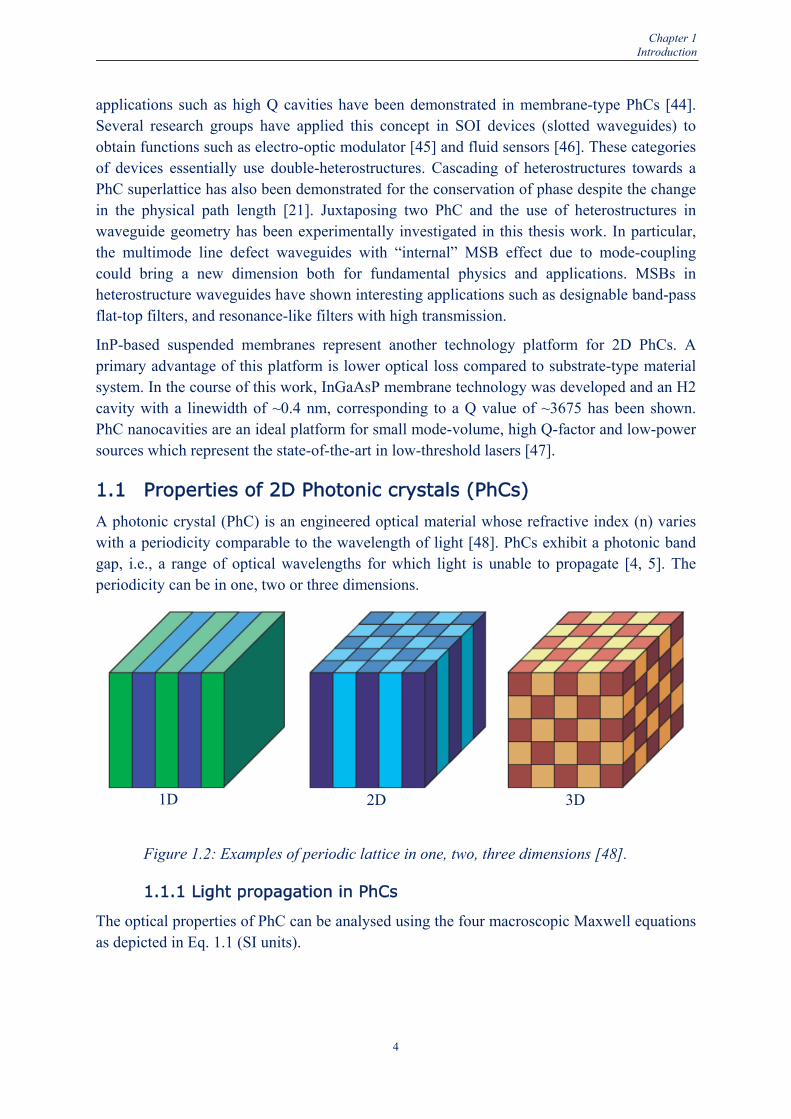
A photonic crystal (PhC) is an engineered optical material whose refractive index (n) varies with a periodicity comparable to the wavelength of light [48]. PhCs exhibit a photonic band gap, i.e., a range of optical wavelengths for which light is unable to propagate [4, 5]. The periodicity can be in one, two or three dimensions.
Figure 1.2: Examples of periodic lattice in one, two, three dimensions [48].
1.1.1 Light propagation in PhCs
The optical properties of PhC can be analysed using the four macroscopic Maxwell equations as depicted in Eq. 1.1 (SI units).
2D 1D 3D

5
Chapter 1Introduction
∙ 0 0
∙
1.1
where (respectively) E and H are the macroscopic electric and magnetic fields, D and B are
the displacement and magnetic induction fields, and ρ and J are the free charge and current
densities. The materials of interest are non-magnetic dielectric with negligible density of charge. Therefore, being restricted to linear, lossless and isotropic material, with these
assumptions ρ = 0, J = 0, D(r)=(r)E(r) and B=H. The Maxwell equations (1.1) become
∙ , 0 ,
,0
∙ , 0 ,,
0
1.2
By introducing time dependence of H and E as a harmonic oscillating function i.e.
,
, 1.3
Substituting this expression into the two curl equations of 1.2 will relate E(r) to H(r):
0
0 1.4
These equations can be decoupled by dividing the bottom equation of 1.4 with
ε(r), and then taking the curl. Thereby, using the first equation to eliminate resulting in
an equation entirely in :
1
1.5
This equation is known as the master equation which completely determines . The master equation converts the physics of Maxwell equations into an eigenvalue condition
(Maxwell operator Θ , eigenvectors and eigenvalues (ω/c)2) on the
harmonic magnetic modes . For a given frequency, we can solve for and then
determine the by using second of equation 1.4 as given below:
1.6
We can also decouple 1.4 for the electric field but the solution is a generalized eigenequation. It is far more difficult numerical task to solve a generalized eigenvalue problem than an ordinary eigenvalue problem; therefore rendering this approach is not practical. The treatment of light propagation in PhCs follows the description in ref. 48.

6
Chapter 1Introduction
1.1.2 The 2D PhC lattice
In particular, this thesis is focused on 2D PhCs. The PhC patterns etched into the dielectric material, i.e. an InP-based heterostructure, is a triangular lattice of circular air holes. The lattice constant ( ) and the radius of the hole ( ) are defined on Fig. 1.3. The air filling factor (f) is an important parameter in the PhC design as the
Figure 1.3: The triangular lattice.
photonic band gap in the optical spectrum as well as the optical loss depends on the volume occupied by the air and is a function of ‘ / ’. It is calculated from a unit cell and is given by:
2
√3 1.7
The reciprocal lattice is also a triangular lattice but rotated 90° with basis vector f and f
constructed from real space basis vectors e a, 0 and e , √ and are given by
f 1,√
and f√, 0 . The first brillouin zone (BZ) in the reciprocal space is a
hexagon. The points M and K at the edge of the BZ are high symmetry points of the reciprocal lattice. An illustration of the real and reciprocal lattice is shown in Fig. 1.3.
1.1.3 Light propagation in 2D PhCs
The photonic band structure computation is the solution of the master equation for the perfect PhC, i.e., for an infinitely extended, strictly periodic array of dielectric material. In a 2D PhC, two distinct polarization states TE ( 0) and TM ( 0) can be
defined. Here, we consider 2D PhCs only in the TE-polarized case which is most relevant for

7
Chapter 1Introduction
triangular lattice of air holes described above. In this case the master equation reduces to a single scalar equation for the z-component of the magnetic field, [49].
1 1
0 1.8
Equation 1.8 represents a differential equation with periodic coefficients. Subsequently, its solution obeys the Bloch-Floquet (BF) theorem [50,51]: The discrete translational symmetry
of the lattice allows the solutions with a wavevector that is restricted to the first BZ of the
reciprocal lattice. In virtue of the BF theorem, can be expanded into a sum of plane waves. For simplicity, consider a structure periodic in the z direction, with period:
1.9
where u(z) is a periodic function of z, with period a. This means that u(z+a)=u(z). This defines Bloch boundary conditions in one dimension and this condition can be generalized to two or three dimensions in a straightforward way. The photonic band structure is calculated
by determining the angular frequencies,ω k , as a function of wavevector k for all the
Bloch modes in a given frequency range.
1.1.4 Plane Wave Expansion (PWE) method
The method based on the model discussed above is so-called Plane Wave Expansion (PWE) [52]. It takes advantage of the periodicity of the structure and solves the TE master equation 1.8 in the frequency domain and particularly successful to obtain PhC band structure. One drawback is that it cannot be used when BF-theorem does not apply, i.e., if the structure is far from a perfect periodicity or finite size or boundary conditions begin to dominate. Nevertheless, it is possible to simulate cavities or straight waveguides by implementation of supercell method [53,54].
1.1.5 The Band structure
The performance of PWE method is demonstrated by the results of the mode calculations shown in Figure 1.4. The band structure is for TE-polarized radiation in a 2D PhC consisting of a triangular lattice of cylindrical air pores (f=40%) in a InP-based material matrix (n=3.24). Because of the six-fold symmetry of the reciprocal lattice, the PhC modes need to
be calculated only for k-vectors along the edge of the irreducible BZ.
The structure exhibit a complete 2D band gap. The low-frequency modes concentrate their energy in the high- region; therefore, the band below the gap has its power concentrated in the dielectric material which is called the “dielectric band.” The band above the band gap concentrates its power in air. It is referred to as “air band.” This fundamental band gap has a gap-to-midgap ratio 45% and extends between u=0.22 to u=0.35; where ‘u’ is the normalized frequency equals to ‘a/λ’ and ‘a’ is the lattice period. Selecting a lattice constant of 420 nm corresponds to an operating wavelength window of 700 nm around 1.55 μm.

8
Chapter 1Introduction
Similarly, TM band gaps are favoured in a lattice of isolated high-ε regions (pillar-type). In this case, the electric field has only a z-component E and we may work with the corresponding wave equation:
1
0 1.10
Figure 1.4: Photonic band structure for TE-polarized light in a triangular lattice of air holes in dielectric with n=3.24 for an air fill factor of 40%.
1.1.6 InGaAsP/InP material system
InP-based material system is used for the practical implementation of 2D PhC. The well established approach based on planar waveguide structure was used [6]. A planar dielectric waveguide consists of a layered structure of lossless dielectric materials with different refractive indices and can support the propagation of light along the plane of the layers. The guiding layer has a high n compared to lower and upper cladding layer as shown in Fig. 1.5. The planar waveguide used in this thesis is similar to that used in semiconductor lasers or integrated optics devices. Hence, the integration of PhC structures is relatively easy task. For details on the fabrication of this structure, the reader is referred to chapter 2 of this thesis.
The width and effective refractive index (neff) of the guided mode depends on the thickness of the core layer and the difference of the refractive index between the core and cladding. The devices discussed in this thesis were fabricated from InP-based planar waveguides with vertical index difference ~0.2. The width of the core layer is determined by the requirement of single guided mode. If the thickness of the core layer is too large, more than one mode can be guided by the planar guide. Typical core layer thicknesses used in this thesis are 420 and 522 nm. The intensity profile of the guided mode in these two core systems are shown in Fig. 1.6.

9
Chapter 1Introduction
Figure 1.5: 2D PhC based on planar waveguide structure.
The effective index or model index (neff) which is not just a material property, but depends on the whole waveguide design is ~3.24 for both vertical structures. The mode has a bell shape profile and penetrates into the cladding layer. A common approximation is that the neff is a weighted average of n in the core and cladding of the waveguide with weight factors determined by the fractions of the optical power in the core and cladding.
Figure 1. 6: Finite difference (FD) simulated Hz mode distribution for (a) tcore=420 nm and tclad=200 nm (b) tcore=522 nm and tclad=300 nm.
A complete description of functional devices such as mirrors, waveguide and resonators based on this structure would require full 3D simulations. For most of the PhC properties, such as the spectral position and size of the band gap, a corresponding 2D system can be investigated, where the dielectric material has an effective refractive index of the

10
Chapter 1Introduction
fundamental guided mode of the planar waveguide. In this thesis, a 2D model combined with the effective index approximations is considered [55].
1.2 Outline of this thesis
In this chapter, an overview of the field and various basic properties of PhCs have been discussed. The remaining sections of the thesis is organised as follows. Chapter 2 elaborates on the fabrication of 2D PhC devices including a description of techniques used to manufacture them. Technology development for InGaAsP suspended membrane and resonant modes of an optically pumped PhC H2-cavity are presented. A post-etch fabrication technology based on so-called mass transport effect is elaborated in chapter 3. Chapter 4 describes several interesting properties of PhC waveguides using high quality PhC fabrication technology described in the previous chapter. Novel device applications are discussed. Chapter 5 summarizes the conclusion and detailed suggestions for future work. Finally, the chapter 6 describes the original work and summarizes the appended papers.

11
CHAPTER2FABRICATIONTECHNOLOGY
From the very start of the research on photonic crystals (PhCs), two-dimensional (2D) structures have been one of the major areas of investigation mainly due to the mature fabrication technology. In contrast, the fabrication of genuine 3D PhCs is more difficult and cumbersome. However an ideal 2D PhC consists of a periodic array of infinitely long holes or rods so that the structure which approximates this theoretical model has to exhibit very high aspect ratios. Structures with aspect ratios up to 10-20 are feasible using the conventional dry etching technique. The PhC slab structures were developed to avoid scattering of light out of the plane of periodicity and to reduce the corresponding loss. The fabrication of 2D PhCs involves several relevant process steps that are detailed in this chapter along with the results of the fabrication for InP/InGaAsP material system, which is the most prominent candidate for devices incorporating gain elements at 1.55 μm.
2D PhC fabrication
2D PhCs are realized as air hole patterns in InP/InGaAsP material systems. High-contrast PhCs operated at 1.55 μm wavelength region involve periods of about 400 to 600 nm. Air filling factors of 30-40 % are used to maintain sufficient waveguiding in the core layers resulting in hole diameters of about 150 to 350 nm. Two types of InP-based material systems are used in this present work:
Low vertical contrast material system (Substrate-type)
High vertical contrast material system (Membrane-type)
The InP/InGaAsP/InP slab structure was grown by metal organic vapor phase epitaxy on a InP substrate. The core layer in substrate-type material system, In0.76Ga0.24As0.52P0.48, is lattice matched to InP substrate and has its absorption edge at λedge=1.22 μm. In membrane-type material system, the same InGaAsP material is grown for 250 nm thick guiding layer. For both of these material systems, the patterning process consists of three major steps:
Definition of a resist pattern by lithography
Transfer of the resist pattern into the mask by reactive ion etching (RIE)
Transfer of the dry etch mask into the waveguide layer by highly anisotropic etching

12
Chapter 2Fabrication Technology
Section 2.1 describes the fabrication of substrate-type PhC with its sub-sections explaining the technique for the appropriate process. Deposition of hard mask is explained in 2.1.1. Sub-section 2.1.2 illustrates how 2D PhC devices can be accurately patterned with advanced lithography method. The transfer of such patterns from the electron-beam resist into an underlying material using plasma etching is described in 2.1.3 and 2.1.4. Electron microscopy of fabricated nano-structures is explained in 2.1.5. Manufacturing of membrane-type PhC is explained in section 2.2 with dry etching introduced in section 2.2.1 and wet-etching process discussed in 2.2.2. Finally, section 2.3 describes an H2 PhC nanocavity in the InGaAsP suspended membrane.
2.1 Low vertical contrast InP-based material system (Substrate-type)
In substrate-type material system the refractive index contrast is about 0.2 (InP/InGaAsP) resulting in weak vertical confinement of light. This semiconductor heterostructure approach has a variety of advantages, e.g. simplicity, mechanical stability and, most importantly, it allows current injection. The main drawback, however, is the fact that the light is rather weakly confined by the limited refractive index contrast available with a semiconductor heterostructure, and, in a PhC, it will scatter into the substrate. For in-plane PhCs, a patterning technology is needed which can reliably control critical dimensions to an accuracy of sub-10 nm.
2.1.1 Plasma-enhanced chemical vapor deposition (PECVD) of the hard mask
Amorphous high density SiOx and SiNx are good masking materials for InP-based materials because they offer a low resistance against the fluorine-based mask etching and a high resistance against chlorine-based semiconductor etching that are used to transfer the lithographically defined patterns. Masking strategies involve hard mask layers of sufficient thickness which are etched after by RIE using fluorine-based chemistry (section 2.1.3). PECVD allows deposition of thin films (SiOx or SiNx) at relatively low process temperature because the reactive species are generated by coupling of energies through plasma. The maximum thickness of the hard mask that needs to be provided for etching underlying InP is limited by plasma-etch selectivity of the resist verses the hard mask. SiO2 hard mask has slightly better selectivity as compared to SiNx. A 260 nm thick layer of silicon oxide (SiOx) hard mask is deposited on InP using PECVD. The thickness of the layer is large enough to allow deep etching which is an essential requirement of substrate-type material system. The etching of the underlying InP material is discussed in section 2.1.3 and 2.1.4. Silane is used as silicon source and nitrogen peroxide is used as oxygen source. The reaction taking place is
→ 2 2 2.1
Silicon oxide doesn’t have exactly ½ Si/O ratios. This ratio is very sensitive to process conditions. We use 2 % nitrogen in silane flow to improve the quality of deposited silicon oxide layer. Complete deposition parameters are listed in table 2.1 in section 2.1.3.

13
Chapter 2Fabrication Technology
2.1.2 Electron beam lithography
Electron beam (e-beam) lithography is most suited for prototyping of densely integrated optics and 2D PhCs due to its combination of flexibility and patterning accuracy. The properties of 2D PhC devices depend strongly on the exact radii of holes and their uniformity. For waveguiding, recent investigations have shown that in InP substrate-type material system, sub-nanometer variation in the hole-radius effects the optical properties [56].
Figure 2.1: Schematic of the Raith Turnkey 150 e-beam lithography system
Pattern definition of nanostructures was realized on a Raith Turnkey 150 e-beam lithography system at the joint KTH and SU laboratory facility at Albanova. The e-beam lithography system consists of a Scanning Electron Microscope (SEM) integrated with a beam blanker and a pattern generator unit. Raith 150, version 5.0, software was used to controls the system hardware, off-line design of structures and proximity correction. The SEM is a LEO 1520 system with a Gemini column which is specially built to give high precision and performance at low accelerating voltages. The acceleration voltage can be set from 200 V to 30 kV. The column is equipped with a field-emission electron source. A schematic drawing of the e-beam system is provided in Fig. 2.1.
The transfer of the resist patterns into the dry etch mask forces the use of resist layers; thereby resulting in a demand for high resolution lithography in regards to resists. E-beam resists are available but they differ in terms of resolution, sensitivity or resistance to dry-etching. Generally, resists can be categorized in two types; positive resist and negative resist. In this work, only positive polymer based resist ZEP520A is used which is high performance e-beam resists that exhibits high resolution, high sensitivity and dry etch resistance. The resist is spun coated at 4000 rpm, prebaked at 180°C and developed in p-xylene after e-beam exposure. Whereas for high-end e-beam systems with 100KV accelerating voltage thick resist

14
Chapter 2Fabrication Technology
layers (up to 1 μm) can be used [57], the maximum resist thickness for accurate patterning with 30 KV e-beam system, as in our case, is in the range of 300-400 nm.
The dose is the amount of electrical charges received by the resist per unit area (μC/cm2). One of the characteristic figures of the e-beam lithography process is the critical dose. It is defined as the charge deposited by the electron-beam in order for the exposed regions to be removed completely by the developer. When electrons accelerate with a certain voltage penetrate into a material, they are subjected to back and forward scattering. Some of the incident electrons are scattered with a very large angle and are responsible for the exposure of the resist in areas away from the actual beam position. The additional dose resulting from back-scattered electrons give rise to the proximity effect (PE) which is the main limiting factor for e-beam lithography accuracy [58]. The magnitude of this effect is dependent on the accelerating voltage. High accelerating voltages (50-100 kV) reduces PE due to a larger penetration depth of the electrons in the substrate material. In this case, the large angle scattering occurs further away from the resist with the probability of them becoming absorbed in the material before reaching the resist is much higher. However, this is not the case for lower accelerating voltages; thereby a 25 KV (which is used in the present work) accelerating voltage causes a more pronounced PE.
In the case of exposure over large areas, a writing field alignment (WFA) has to be performed. The reason for the WFA is that the signal to deflect the beam is passing through several stages which all have more or less of long term drift. It is the adjustment of the electromagnetic/electrostatic deflections system inside the column to the high precision X-Y-Z stage. The stage is considered to be correct and the e-beam deflection system is aligned to it. A small feature on the sample or a reference sample is placed at the center of the given write field corresponding to the center of the column for zero deflection. Hence, the system moves the stage in order to position the feature at one of the WF corner. WFA is performed manually followed by an automatic alignment procedure with images for a minimum scan size of 1 μm. WF stitching errors as small as ~20 nm has been achieved in most of the exposures. In general, lithography for PhCs is challenging but not considered a roadblock in PhC field.
2.1.3 Reactive ion etching (RIE) of a hard mask
Surface structuring by wet or dry etching is one of the basic steps in semiconductor fabrication. Wet chemical etching offers selectivity to materials and/or crystalline directions, whereas, dry plasma etching allows high fidelity pattern transfer from a lithographically defined mask. Dry etching advantage as opposed to wet etching is that it provides greater control, etch anisotropy and lateral etch rates very close to zero. This is essential when nano-scale features with a high aspect ratio have to be fabricated.
Plasma is an electrically neutral, ionized gas composed of ions, electrons, and neutral particles. It can be created by applying a sufficiently strong alternating electromagnetic field between two electrodes of a capacitor. The regime of interest to semiconductor processing is the low-pressure plasma or glow discharge. These plasmas are characterized by gas pressures~50-500 mTorr, ion densities ~1010 cm-2, and electron energies ~1-10 eV. Most industrial RIE reactors use 13.56 MHz radio-frequency (RF) power which is higher than the

15
Chapter 2Fabrication Technology
Figure 2.2: Schematic of plasma reactor used in this work.
ion plasma frequency. Consequently, ions cannot follow the applied field therefore respond only to the time average cathode voltage resulting in a self-bias that arise between the electrodes which is referred to as plasma potential. The potential difference generates strong DC electric fields in the region between the electrodes, and, accelerates positively charged ions towards the sample on the electrode. A schematic of the plasma reactor used in this work is shown in Fig. 2.2.
Method PECVD RIE
Electrode/Substrate temperature (°C)
300 20
Pressure (mT) 800 20
RF power (W) 20 100
DC Bias (V) - 350
Gas 1
Flow (sccm)
SiH4
710
CHF3
25
Gas 2
Flow (sccm)
N2O
425
-
Duration (min) 04:00 30:00
Table 2.1: Parameters for plasma processes; SiOx hard mask deposition (PECVD) and etching (RIE).

16
Chapter 2Fabrication Technology
RIE is a dry etching technique in which energetic chemical reactivity species causes material selective reaction which generates volatile products that can be desorbed. Plasma etching of SiOx or SiNx is a trivial process in microelectronics fabrication and uses fluorocarbon gases; CHF3 [59, 60], CF4 [61], C2F6 [62], C3F8 [62]. To achieve certain etch characteristics (e.g., verticality, selectivity, etch rates) additives such as O2, H2 or N2 are commonly utilized. In this work, a CHF3-based process was chosen for etching the hard-mask because this gas offers excellent selectivity between ZEP520A photo resist and SiO2. The key parameters of the process are listed in table 2.1.
2.1.4 Chemically assisted ion beam etching of substrate-type PhCs
In substrate-type material system, the refractive index contrast is about 0.2 (InP/InGaAsP) requiring PhC hole depths significantly deeper than the waveguide core thickness (~3-4 μm). From fabrication perspective, a high aspect ratio of the distances between adjacent holes represents the most important figure of merit of patterning. Substrate-type materials system based on slab waveguides require aspect ratios >10. In addition, the shape of the hole has to be well-defined over the entire interaction length with the guided mode. Variations of the parameters over the PhC area, especially close to their boundaries, must be kept small.
The fabrication of PhCs with a high aspect ratio forces the use of highly directional etching technologies which prevents the use of partially isotropic dry etching process, e.g., RIE. Appropriate options include inductively coupled plasma based RIE (ICP-RIE), electron cyclotron resonance enhanced RIE (ECR-RIE) and chemically assisted ion beam etching (CAIBE); amongst these etching techniques only CAIBE provides an independent control over the chemical and physical etch mechanisms. The CAIBE process combines a highly anisotropic physical etching component with a chemical component which can be independently tuned that allows the etching of PhC-holes with a well-controlled nearly cylindrical shape.
CAIBE technique relies on the bombardment of a sample with a chemically inert ion beam in a reactive gas atmosphere having pressures ~10-4 torr range. In this work, the neutral gas is argon (Ar) and the reactive species is chlorine (Cl2). Cl2 is injected via a gas ring over the sample and Ar ions are extracted from remote plasma. In the Ar/Cl2 CAIBE process, the sample is subjected to a directional Ar flux, in the ambient of reactive Cl2, close to molecular flow regime. For a useful etching process, all atomic species have to be removed at the same rate. In contrast to Si, the etching of InP-based materials is affected by PClx etching products of varying vapor pressures while one component, InCl3, is non-volatile at room temperature. To remove etch products of low volatility, desorption can be promoted by increasing process temperature and by Ar ion beam sputtering that maintains the process anisotropic at a speed comparable to that of chemical etching. The side walls are protected as long as they are not hit by Ar atoms. The balanced removal of the InClx and PClx materials is most important for high-aspect-ratio etching.

17
Chapter 2Fabrication Technology
Figure 2.3: Schematic diagram of the two-grid Nordiko 3000 ion beam etching system.
A two-grid Nordiko 3000 ion beam etching system is used in this work. In this system, the plasma is generated by inductively coupling of the RF power (13.56 MHz) through a dielectric window by a flat coil antenna. The substrate holder can be rotated with respect to the ion beam axis. It allows the variation of the sample orientation by tilting the sample holder. A set of two perforated grids is used to extract the ions from the plasma and accelerate them towards the sample. The positive grid as well as the walls of the plasma chamber is at the potential (V+). The negative grid is isolated from the chamber and has a negative potential (V-) kept at -100V. The distance between the two grids is approximately 1 mm. The low energy ions (~10 eV) extracted from the plasma impinge on the positive grid diffuse through the openings of the positive grid and acquire an energy (qV+) which is kept at 400 eV for all etching processes. This is the energy that the ions bombard the sample with; as the sample holder is grounded. The collimated ion beam has a diameter 3 cm adjusted by a diaphragm. An electron gun is used to neutralize the ions in the beam and reduce the beam divergence which is due to coulomb repulsion between the ions. The base pressure in the chamber is ~10-8 torr; maintained by a turbo-molecular pump backed by a mechanical pump. A schematic diagram of the system is shown in Fig. 2.3.
At room temperature, desorption of InClx is very low. The difference in masses between In and P atoms results in a large difference in their partial sputtering yields that gives preferential sputtering of the lighter phosphorus atoms. The imbalance progressively increases due to the low volatility of In resulting in clustering of In atoms. The access In atoms are able to migrate at the surface and form clusters together with InClx compounds (Fig. 2.4). This will induce In enrichment of the surface [32]. Desorption of the InClx byproducts can be enhanced at elevated temperatures (>150) thereby reducing this micromasking effect. A precise control of this operating point (180-200°C) requires a precise

18
Chapter 2Fabrication Technology
Figure 2.4: SEM top-view showing room temperature etching of a ridge waveguide. Micromasking effect is clear in etched trench.
control of the wafer temperature, i.e., the use of wafer cooling and heating systems. In the present case, the sample is heated radiativly using a halogen lamp.
Etching of nanostructures such as PhC-holes differs from etching extended structures such as ridge waveguides. In the case of ridge waveguides, the etched atoms can leave the surface into a large solid angle, which results in large etch rates and good selectivity. In contrast, the transport of the material out of deep holes is limited to small solid angles. Therefore, the etch rates and the selectivity of the mask verses semiconductor decreases with increasing etch depth. Argon-chlorine based CAIBE (Ar/Cl2 CAIBE) process is one of the most successful processes for high aspect ratio etching of nanostructures. Figure 2.5 shows the SEM cross-sectional images of deeply etched 1D and 2D PhCs.
Figure 2.5: SEM cross-sectional view of deeply etched (a) 1D and (b) 2D PhCs.

19
Chapter 2Fabrication Technology
2.1.5 Scanning Electron Microscopy (SEM) analysis of Fabricated Samples
As methods of investigation, scanning electron microscopy (SEM) is one of the most popular and widely used tools for structural and material characterization of nanostructures. It images the sample surface by scanning it with a high-energy beam of electrons in a raster scan pattern. The electrons interact with the atoms that make up the sample producing signals that contain information about the sample's surface topography, composition and other properties such as electrical conductivity. The types of signals produced by an SEM include secondary electrons, back scattered electrons (BSE), characteristic x-rays, light (cathode-luminescence), specimen current and transmitted electrons. The signals result from interactions of the electron beam with atoms at or near the surface of the sample. When a primary electron beam hits the sample, certain interaction products are recorded by means of specific detectors to be used for the generation of images. The interaction products used most frequently for the generation of images in scanning electron microscopy are the secondary (SE) and back-scattered electrons (BSE). Secondary electrons are generated by inelastic scattering of the primary electrons on the atomic core or on the electrons of the atomic shell of the sample material. Secondary electrons are low energy electrons with energies <50 eV. Depending on the mode of origin and the range where they leave the sample, they are subdivided in different groups. The list below defines the three most important groups.
SE1: are generated / leave the specimen surface directly in the spot centre
SE2: are generated after multiple scattering and leave the surface at a greater distance from the spot centre
SE3: are generated by BSE at places far away from the spot centre and do not contribute to essential image information
SEM is often coupled with X-ray analyzers that are used to identify chemical composition within the sample. High energy electron beam generate X-rays on interaction with sample which are characteristic of the elements presenting in the sample and determine the local chemical composition of the samples. This is known as energy dispersive X-ray spectroscopy (EDS) which is based on summation and X-ray energy. Depending on the exact choice of the beam energy, a good lateral spatial and depth resolution can be obtained on a scale ranging from micrometers to nanometers. The stoichiometry of the surfaces on the cross-section of PhH3/AsH3 annealed PhCs has been analyzed by SEM-EDS.
For high resolution imaging of PhCs, optimization of parameters such as beam diameter (spot size), depth of field and signal strength is critical. Depth of field as well as high resolution is required especially for cross-sectional study of several µm deep holes. The spot size is controlled by changing the working distance. The image resolution depends on spot size. The resolution of the specimen is decreased by increasing the working distance because the spot size is increased. Conversely, the depth of field is increased with an increased working distance due to the divergence angle becoming smaller. Therefore, a compromise is made between resolution, depth of field and signal strength for imaging of these nanostructures.

20
Chapter 2Fabrication Technology
In this present work, the ULTRA FE-SEM from Carl Zeiss NTS GmbH is used for topographic imaging and for compositional contrast imaging. To map the actual surface of the sample, SE electrons of type 1 and 2 should be detected as these are the only electrons generated directly in or near the spot center. These electrons can be detected very efficiently by using the In-lens detector, whose detection efficiency results from its geometric position in the beam path and from the combination with the electrostatic/electromagnetic lens. The detector is placed above the objective lens and detects directly in the beam path. An accelerating voltage of 1-1.8 kV is used with a working distance of 1.5–2.5 mm. For SEM-EDS analysis, SE2 detector is used, with the sample kept at working distance of 8.5 mm and the accelerating voltage adjusted between 8–15 kV. An in-lens detector image of the tilted cross-section of PhC etched with CAIBE is shown in Fig. 2.6. The contrast in the core-region of the hole is due to different elemental compositions of the material. Energy-Dispersive Spectra (EDS) caused by the X-rays generated from the labeled scan area of the SEM image displays the characteristics peaks of the corresponding elements.
Figure 2.6: (a) High contrast SEM image taken with In-lens SE detector. The contrast at the core region of the hole is due to different elemental compositions of the material. (b) Energy-Dispersive Spectra caused by the X-rays generated from the labeled scan area of the SEM image.

21
Chapter 2Fabrication Technology
2.2 High vertical contrast InP-based material system (Membrane-type)
High vertical index contrast (∆n ≥2) enables tightly confined light and it is advantageous for low optical loss. Table 2.2 summarizes some of the commonly used high vertical contrast material systems. Among all of these material systems, InGaAsP membrane is the only system capable of implementing active devices using gain element at 1.55 µm. InGaAsP membrane technology has been developed in house and the fabrication process consists of following steps:
Epitaxial structure: 50 nm cap of InP, 240 nm thick device layer of In0.76Ga0.24As0.52P0.48 lattice matched to InP, and 400 nm buffer layer was grown by MOVPE.
Lithography and etching: Definition of a resist pattern by lithography, transfer of the resist pattern into the dry etch mask by RIE-etching and subsequently transfer of the dry etch mask into the waveguide layer by ICP-RIE.
Selective wet etching: Removing the underlying material by chemical etching.
Material system
Core Underlying material
∆n
Silicon on insulator (SOI)
Silicon SiO2 2.05
GaAs membrane
GaAs Air 2.37
InP membrane InP Air 2.17
InGaAsP membrane
InGaAsP Air 2.4
Table 2.2: Examples of high vertical index contrast material systems.
2.2.1 Inductively coupled plasma based RIE for fabrication of membrane
Inductively coupled plasma (ICP) reactive ion etching (RIE) has become well known for etching InP based structures. Its ability to provide gentle processing environment (low temperatures and pressures; and mild voltages) can prevent unwanted diffusion and degradation of materials due to heat and lattice damage as a result of ion bombardment. Two different RF power sources independently control the plasma density and the ion energy. Energy is coupled inductively into the plasma by a coil around the chamber. The ion energy is monitored by adjusting bias voltage generated on lower electrode which, therefore, is controlled by RF power supplied to this electrode. The ICP source controls the density of ions/reactive species at relatively low pressures. Vertical etching can be achieved, when ICP-

22
Chapter 2Fabrication Technology
Figure 2.7: Schematic diagram of the Oxford Plasma lab’s ICP380 Etch System.
RIE is utilized, as the ions hit the sample at approximately normal incidence. The energetic ions can etch the underlying material chemically by forming volatile etch products and physically by removing the atoms by sputtering. Introducing the inert ions in the etching chemistry enhances the physical sputtering.
Oxford Instrument ICP380 Etch System is used in this work. RF power (13.56 MHz) is applied to both sources. ICP source up to 3000 W and substrate electrode up to 600 W generate the etch plasma. A loadlock is used for wafer loading that ensures good stability of the vacuum of the chamber; thereby enhancing the reproducibility of the etching outcomes. The samples being etched are attached on a 3 inch Si carrier wafer with thermally conductive glue. After clamping the wafer to a temperature-controlled lower electrode, helium pressure is applied to the back of the wafer to provide a proper thermal conductance between the wafer and the chuk. Good temperature control is required to control the volatility of the etch species that can affect etch rate, selectivity and surface roughness. The system operates over a pressure range of 1-100 mT. A schematic of the system is shown in Fig. 2.7.
Figure 2.8 shows the self bias voltage versus RF-power applied to the substrate for different RF-powers fed into the ICP-antenna. The RF-power delivered to the ICP antenna controls the density of the accelerated ions. Screening effect lead to a decreasing self bias voltage with increasing ions, i.e., plamsa density. An increasing RF-power at the substrate leads to an increasing separation of electrons and ions in the plasma and thus leads to an increasing self bias voltage. The ICP source creates high-density plasma at low pressures. The generated ion energy is independently controlled by the bias on the substrate electrode. This allows the

23
Chapter 2Fabrication Technology
Figure 2.8: (a) Self bias voltage Vbias vs. Radio frequency power PR.F fed into the substrate for various RF-powers PICP applied to the ICP-antenna.
acceleration of both chemically active and inert ions on the substrate and thereby combines chemical and physical etch mechanisms.
Parameters Recipe 1 Recipe 2
Pressure (mT) 4 4
RF power (W) 180 100
ICP power (W) 2800 1000
DC Bias (V) 380 260
Gas 1
Flow (sccm)
Cl2
7
Cl2
9
Gas 2
Flow (sccm)
CH4
5
CH4
5.5
Gas 3
Flow (sccm)
H2
5
H2
7.5
Gas 4
Flow (sccm)
Ar
5
-
Etch rate (nm/min) 1200 330
Table 2.3: Parameters for two different optimized ICP-RIE plasma processes for vertical side wall etching.

24
Chapter 2Fabrication Technology
Although the physical parameters such as power and pressure significantly control the etch profile, the gas chemistry is the most essential component for an etch process. A wide range of chemistries can be used for the same substrate. In general III–V materials require the use of chlorine-based chemistries. The recipes used in this work contain CH4, Ar, H2 and Cl2. The gas composition of this etching recipe is a hybrid between two established InP recipes: (1) High etch rate recipes with Cl2- and Cl2/Ar-based plasmas that generally suffer from sidewall roughness and require high processing temperatures to volatilize InClx species. (2) Smooth etch recipes with CH4/H2 plasmas with very slow etch rates. The details of the optimized key parameters for the two etch recipes used in this work are listed in table 2.3.
An optimized ICP-RIE etching process must provide highly vertical structures to ensure low optical loss. Optimization of the etching recipes for nanostructures such as PhC-holes is performed with and without Ar dilution of the plasma. By using a Si carrier, a SiOx passivation layer forms on the sidewall and is enhanced by H2 gas, therefore, further improving the anisotropic etching [63]. Recipe 1 benefits from physical etch component as a result of Ar ion bombardment. The etch rates are high due to high plasma powers. Recipe 2 is optimized to achieve highly vertical sidewall profiles upto 1µm as shown in Fig. 2.7(b). The optimization of both the recipes is performed at room temperature.
Figure 2.9: SEM cross-sectional view of 2D PhCs etched with two different optimized recipes (a) Recipe 1 and (b) recipe 2.
2.2.2 Selective wet etching to fabricate PhC membrane
After the etching of the PhC patterns through the InGaAsP device layer, the underneath InP material is removed by an isotropic chemical etching with HCl diluted in water (HCl:H2O 1:2) through the fabricated holes. This etch solution is highly selective against InP therefore preferentially favoring InGaAsP. This procedure leaves an air-bridge membrane of perforated InGaAsP slab and creates the membrane-type PhC. The optimized process time of 150 sec completely removes the underlying InP material. Cross-sectional SEM images of the fabricated membrane-type InGaAsP PhCs are shown in Fig. 2.10.

25
Chapter 2Fabrication Technology
Figure 2.10: (a) SEM cross-sectional view of InGaAsP membrane PhCs after selectively removing underlaying InP material. (b) Tilted cross-sectional SEM view showing the complete removal of underlying InP material.
2.3 Active layer structure for InGaAsP membrane
A 240 nm thick quaternary compound semiconductor In0.76Ga0.24As0.52P0.48 membrane, lattice matched to InP was grown by MOVPE. Figure 2.11 shows the SEM cross-section of the fabricated PhC slab. Pseudomorphic strained layer with 0.8% compressively strained 8 nm QW and 0.45% tensile strained 7 nm barriers are used in the active region. Types of active layer structures that are used inside the membrane as light source are as follows:
Figure 2.11: SEM cross-section view of the fabricated InGaAsP-membrane PhC slab.
1: Multiple Quantum-well (MQW) structure: consists of four strain compensated quantum wells adjusted to obtain an emission wavelength ~1550 nm.
2: Single Quantum-well (SQW) structure: consists of one quantum well adjusted to obtain an emission wavelength ~1550 nm.

26
Chapter 2Fabrication Technology
2.3.1 Micro-photoluminescence (μ-PL) spectroscopy of PhC membranes
In order to analyze vertically emission from QWs, the use of μ-PL setup is well known in photonics and optoelectronics. A μ-PL setup is a laser based instrument measuring luminescence from materials excited with energy above their band gap. Single microscope objective lens is used to excite with incident light as well as to collect the emitted light in backscattering geometry. Horiba Jobin-Yvon Labram micro-PL system was used in this work to characterize the QWs. The μ-PL setup consists of a 50x (NA=0.45) microscope objective lens, a monochromator with a liquid-nitrogen-cooled InGaAs detector for PL spectroscopy, and a monitoring CCD-TV camera with a tungsten illumination lamp. The samples are placed in a liquid nitrogen continuous flow cryostat in such a way that the device under test (DUT) faces the objective lens. The optical excitation with a 514 nm line of an Ar+ laser was used in point-excitation mode with a focused spot of ~2-3 μm diameter on the sample surface. A continuous wave excitation power ~100 μW drives an equal rate of excitation and recombination in the active region, and the photo-generated carrier density is constant in time. The measurement configurations used are: (1) room temperature (RT) μ-PL and (2) low temperature (LT) μ-PL (liquid nitrogen cooled).
Figure 2.12: PL spectrum (normalized) of an InGaAsP PhC membrane at room temperature and 77K (a) No active layer (b) MQW active layer. (c) Comparison MQW and SQW at LT.
PL of the fabricated PhC InGaAsP-membrane is analyzed for both setup configurations. Normalized spectra, in case of no active layer buried inside membrane, show band-edge emission wavelength at 1.2 μm as shown in Fig. 2.12(a). Normalization was performed with
1300 1350 1400 1450 1500 1550 16000.0
0.2
0.4
0.6
0.8
1.0
Nor
mal
ized
Inte
nsity
(a.
u.)
Wavelength (nm)
LT MQW PhC membrane
LT SQW PhC membrane
900 1000 1100 1200 13000.0
0.2
0.4
0.6
0.8
1.0
Nor
mal
ized
Inte
nsity
(a.
u.)
Wavelength (nm)
LT InGaAsP PhC membrane
RT InGaAsP PhC membrane
1000 1100 1200 1300 1400 1500 16000.0
0.2
0.4
0.6
0.8
1.0
No
rma
lize
d In
ten
sity
(a
.u.)
Wavelength (nm)
LT MQW PhC membrane RT MQW PhC membrane
(a) (b)
(c)

27
Chapter 2Fabrication Technology
respect to the peak intensity. As expected with reduction in Eg, a red-shift of almost 70 meV is visible with the increase of temperature from LT to RT. PL spectra for a membrane with multiple quantum wells (4 QWs) in the active region shows more rapid shift in the peak emission wavelength in comparison to bulk InGaAsP PhC membrane while reducing the temperature to LT (Fig. 2.12(b)). About 100 nm shift in PL peak wavelength position is observed for both MQW and SQW active layers. Both samples exhibit a LT band edge wavelength at 1425-1450 nm as depicted in Fig. 2.12(c).
2.3.2 Hexagonal defect H2 cavity in PhC membrane
PhC microcavities have recently become a subject of great interest due to possible applications such as low threshold lasers, channel drop filters, nonlinear elements, single photon source, and in experiments involving cavity quantum electrodynamics (CQED) [64-67]. Optical micro- and nanocavities can be also utilized for enhancing light emission of materials [68].
Figure 2.13: (a) SEM top view of the fabricated H2 cavity field. A field size of 25x25 μm is patterned to facilitate both cavity and reference spectrum on the same field. (b) A magnified SEM image of the H2 PhC cavity.
PhC nanocavities consisting of 7 missing air holes (H2) are investigated in InGaAsP-membrane with multi-quantum well (MQW) and single quantum well (SQW) structures. An H2-cavity takes advantage of whispering-gallery-like resonant modes [ 69 ] which have several interesting properties. This large-size cavity has some advantageous features in comparison with single-defect cavities (H1), for example, the introduction of the current post is technically much easier than in H1 cavity and surface recombination loss, the major factor preventing low-threshold operation of single-defect lasers, could be significantly reduced due to enlarged cavity size. Although the cavity area is enlarged compared to H1 cavity case, the mode volume is not drastically increased since the mode is mainly distributed around the cavity boundary. Because of the intensity node at the centre of the whispering-gallery-like modes, the existence of the metallic post does not degrade the Q of the mode. Figure 2.13 shows fabricated PhC H2 cavity.

28
Chapter 2Fabrication Technology
Figure 2.14: Normalized PL spectra for ref. PhC field and H2 PhC cavity. (b) Normalized spectrum for H2-cavity showing resonant modes at 1448.2, 1454.1 and 1487 nm. Normalization was performed by subtracting the ref. PhC spectrum.
Figure 2.14(a) shows a normalized PL spectrum taken at the two positions shown in Fig. 2.13(a). The PL Spectrum measured from these two spots shows QW PL peak at the same position i.e. 1435 nm. Two resonant peaks appear for H2-cavity. Subtracting the background reference PhC spectrum gives clearly visible resonant modes at 1448.2 and 1454 nm as shown in Fig. 2.14(b). The third resonant mode appears at 1487 nm but not very clear being away from the QW luminescence.
Figure 2.15: SEM top view of the fabricated (a) H2 cavity (b) reference field.
The spectral overlap between resonant modes and QW peak position is poor at LT for MQW H2-cavity. To overcome this shortcoming, SQW structure adjusted to obtain a bandedge wavelength of 1450 nm at 77K was used in the second round of device fabrication. In the new design, isolated cavity and reference fields were fabricated as shown in Fig. 2.15(a) and (b) respectively. Line openings were provided on the sides of PhC fields in order to remove the underlying material more effectively.
1350 1375 1400 1425 1450 1475 1500
0.0
0.2
0.4
0.6
0.8
1.0In
tens
ity (
a.u
.)
Wavelength (nm)
H2 PhC cavity Ref. PhC
1430 1440 1450 1460 1470 1480 1490 15000.0
0.2
0.4
0.6
Inte
nsity
(a.
u.)
Wavelength (nm)
(b)(a)
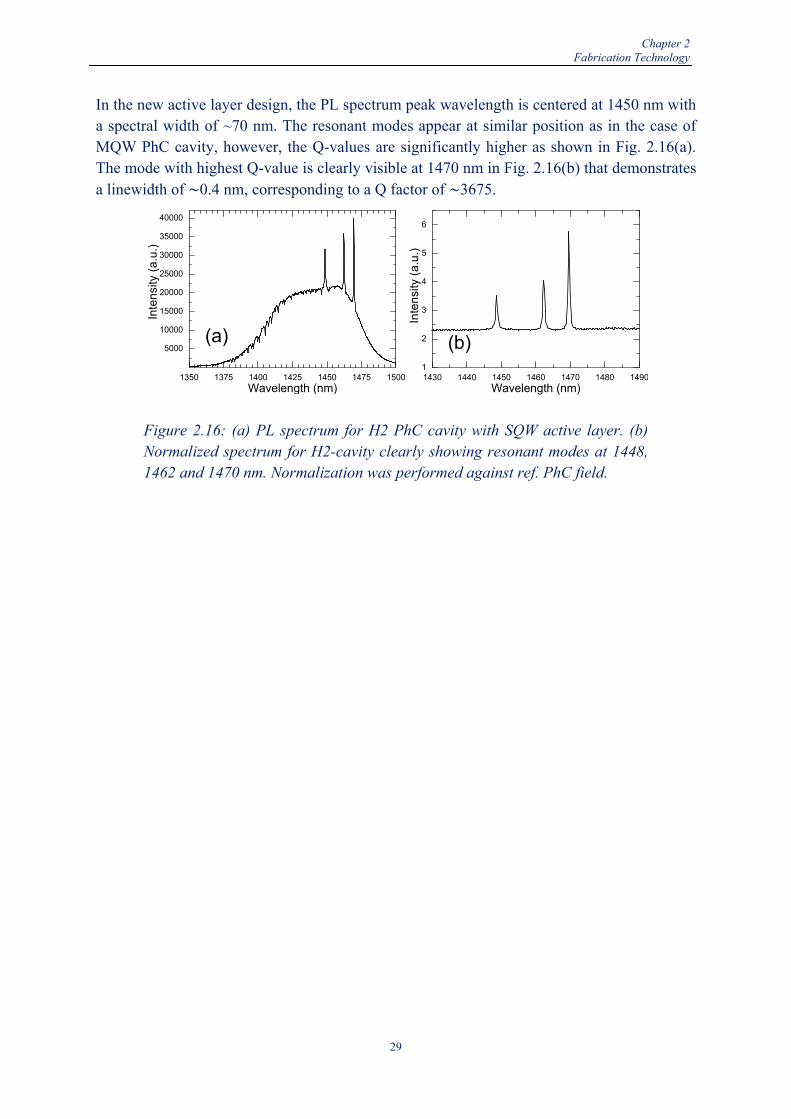
29
Chapter 2Fabrication Technology
In the new active layer design, the PL spectrum peak wavelength is centered at 1450 nm with a spectral width of ~70 nm. The resonant modes appear at similar position as in the case of MQW PhC cavity, however, the Q-values are significantly higher as shown in Fig. 2.16(a). The mode with highest Q-value is clearly visible at 1470 nm in Fig. 2.16(b) that demonstrates a linewidth of ∼0.4 nm, corresponding to a Q factor of ∼3675.
Figure 2.16: (a) PL spectrum for H2 PhC cavity with SQW active layer. (b) Normalized spectrum for H2-cavity clearly showing resonant modes at 1448, 1462 and 1470 nm. Normalization was performed against ref. PhC field.
1350 1375 1400 1425 1450 1475 1500
5000
10000
15000
20000
25000
30000
35000
40000
Inte
nsity
(a.
u.)
Wavelength (nm)1430 1440 1450 1460 1470 1480 14901
2
3
4
5
6
Inte
nsity
(a.
u.)
Wavelength (nm)
(b)(a)
30
CHAPTER3MASSTRANSPORTONINPPHOTONICCRYSTALS
The material system based substrate-type InP/InGaAsP/InP planar waveguide structure is of practical importance for integration due to its compatibility with conventional photonic components (laser, modulator and detector) on InP substrate. Because the vertical light confinement is weak for PhCs in InP/GaInAsP/InP low vertical index contrast structures, etched PhC holes (typically 200-300 nm in diameter) should be cylindrical in shape down to at least 3 µm to ensure good overlap between the modal profile and the PhC holes [32]. It sets a stringent requirement of the dry etching process. In this chapter the reshaping of PhC after complete fabrication as a route to achieve this requirement using a so-called mass transport (MT) process technology has been described.
3.1 Mass Transport (MT) process
Mass transport is a material migration effect that occurs during heat treatment. The phenomenon of mass transport in compound semiconductors was first observed during the fabrication of integrated laser-waveguide structures [70]. Following its discovery, mass transport of InP has been successfully applied to the fabrication of low threshold InGaAsP buried heterostructure diode lasers [71, 72]. This has also been observed on etched structures in GaAs [73] and GaP [74]. This effect has been used as a tool to form several interesting device structures, including buried-heterostructure lasers [71], parabolic mirror facets [75] and micro lenses [74, 76]. Mass transport has also been identified as a major problem in some device fabrication procedures. For example, it causes the flattening of the etched gratings prior to epitaxial growth [77].
Using the CAIBE technique the etched PhCs are invariably either conical or “cylindroconical” with nearly vertical sections on the order of 1–2 μm with the total depth being typically 4 μm. The changes with respect to the aspect ratio and surface quality require the development of novel fabrication processes. Post-fabrication reshaping by mass transport smoothing has been demonstrated for InP-based PhCs for the first time and the results are presented in Paper A.
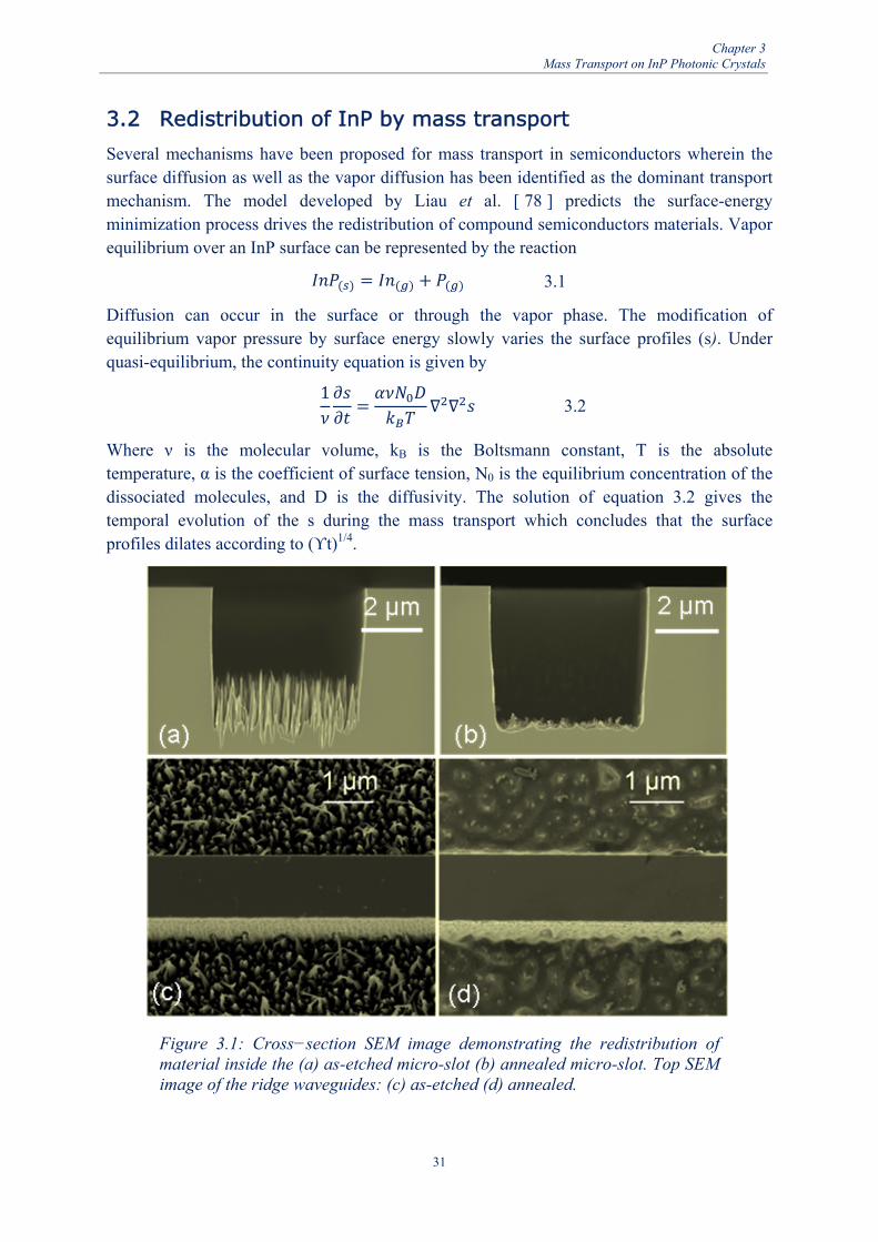
31
Chapter 3Mass Transport on InP Photonic Crystals
3.2 Redistribution of InP by mass transport
Several mechanisms have been proposed for mass transport in semiconductors wherein the surface diffusion as well as the vapor diffusion has been identified as the dominant transport mechanism. The model developed by Liau et al. [ 78 ] predicts the surface-energy minimization process drives the redistribution of compound semiconductors materials. Vapor equilibrium over an InP surface can be represented by the reaction
3.1
Diffusion can occur in the surface or through the vapor phase. The modification of equilibrium vapor pressure by surface energy slowly varies the surface profiles (s). Under quasi-equilibrium, the continuity equation is given by
1
3.2
Where ν is the molecular volume, kB is the Boltsmann constant, T is the absolute temperature, α is the coefficient of surface tension, N0 is the equilibrium concentration of the dissociated molecules, and D is the diffusivity. The solution of equation 3.2 gives the temporal evolution of the s during the mass transport which concludes that the surface profiles dilates according to (ϒt)1/4.
Figure 3.1: Cross−section SEM image demonstrating the redistribution of material inside the (a) as-etched micro-slot (b) annealed micro-slot. Top SEM image of the ridge waveguides: (c) as-etched (d) annealed.

32
Chapter 3Mass Transport on InP Photonic Crystals
Experiments involving InP show that redistribution by mass transport generally produces a rounding of sharply etched edges and filling of narrow voids. A cross-sectional SEM image of an etched slot (Fig. 3.1(a)) shows the grass-like surface roughness in an etched slot which is commonly observed in CAIBE. The redistribution of material in the etched slot flattens the etched surface by the erosion of convex regions and fills-in the concave regions as shown in Fig. 1(b). The top view of a fabricated ridge waveguide is shown in figs. 3.1(c) and 3.1(d). A clear smoothening of the etched bottom-surface surrounding the mesa structure is visible in Fig. 3.1(d). Small surface undulations tend to decrease with the atomic reordering of the etched surface which is driven by minimization of surface energy per unit area (ϒ).
3.3 Annealing of InP-based photonic crystals
After the completion of etching process, InP-based photonic crystals were heat treated for mass transport. This process was performed in a Aixtron 200/4 MOVPE system. All samples were adjusted in the slots created from a 2 inch InP wafer and placed together on the graphite slider.
3.3.1 Annealing under Phosphine (PH3) atmosphere
In InP, the evaporation rate of phosphorus (P) is much higher compared to indium (In). The diffusion of P in the vapor phase is presumably much faster than the diffusion of In atoms on the surface. At elevated temperatures, some decomposition occurs at the surface of InP, requiring a minimum P vapor pressure to be supplied in the ambient to prevent the sample from being transformed into metallic In. The MOVPE system was purged with an overpressure of H2 and PH3 while being heated to 630°C. A 240 sccm PH3 flow was used to prevent decomposition of P during the annealing process.
A combination of various temperatures and time durations are investigated to obtain optimal conditions for mass transport. The optimal conditions for this process were found to be 630°C for 2 min. The system reached 630°C in approximately 10 minutes and remained at the preferred temperature for 2 min before being cooled down.
Figure 3.2: Cross-sectional SEM images of (a) PhC as-etched and (b) reshaped PhC after annealing.

33
Chapter 3Mass Transport on InP Photonic Crystals
Figure 3.2 shows the results obtained for 2D PhCs. Wherein, the comparison in etching was conducted for 2D PhCs having the same geometrical parameters (hole-diameter and period). The as-etched hole profiles (Fig. 3.2(a)) show tapered bottom profiles and irregularities (bending) typical of deeply etched PhCs in InP. The upper part of the etched structure is reasonably vertical as typically observed in dry-etching [32]. In contrast, material reflow not only removes (smooths) any irregularities; but, also results in nearly cylindrical hole profiles that is clearly visible in Fig. 2(b). It is evident that annealing clearly improved the profiles in terms of irregularities and side-wall verticality. The change in profiles is attributed to the reflow of material (i.e. redistribution of material) occurring on the exposed (etched) surfaces. Thus, imperfections in PhC due to variations in feature-size and shape introduced at the pattern transfer step can be effectively reduced using material reflow. The observations clearly demonstrate that material reflow can be used positively to fabricate 2D PhCs with vertical side-walls.
Comparison of the hole or slot profiles shown on Fig. 3.2, suggests that reflow/re-distribution of the material depends on the side-wall angle. The profiles in the upper portion where they are nearly vertical or slightly under-etched are practically unaltered by annealing. This suggests that re-distribution of the material in those regions is not sufficient enough to smoothen out the side-wall roughness. However, the microscopic origin of the roughness in terms of the surface distribution of the elements may also play a role. It is recognized that material reflow depends on the as-etched profile, material composition at the surface and the annealing temperature and duration. Hence, a post-process step could significantly improve the quality of the photonic devices. The superior optical properties of the re-shaped devices are presented in paper A and paper C.
3.3.2 Annealing under Arsine (AsH3) atmosphere
PH3 shows pyrolysis temperatures at 850°C and above whereas; AsH3 undergoes a 50% pyrolysis at a temperature of 600°C and is used to demonstrate reshaping of nanostructures. The AsH3-annealing was performed at lower temperature of 500°C under the same conditions as used in phosphine process (described in section 3.3.1) except that an overflow of arsine was maintained all through the process.
This process reshapes the as-etched profiles which is evident in Fig. 3.3(a). In this figure, the image contrast in the core- and valley-region is due to different elemental composition of the material. The stoichiometry of the surfaces has also been modified after the AsH3-annealing process that is revealed by the SEM-EDS analysis on the cross-section of AsH3 annealed PhC. Energy-dispersive spectra resulted from the generation of X-rays from the labelled scan area of the SEM image shows the characteristics peaks of the corresponding elements (Fig. 3.3(b)) which clearly demonstrates As incorporation in the material.

34
Chapter 3Mass Transport on InP Photonic Crystals
Figure 3.3: (a) High contrast SEM image taken with In-lens SE detector. The contrast at the bottom of the hole is due to different elemental composition of the material inside the valley. (b) Energy-dispersive spectra of the labeled scan area of the SEM image.

35
CHAPTER4PHOTONICCRYSTALDEVICEAPPLICATIONS
Waveguides and filters are fundamental building blocks for PICs. The linear line defects in photonic crystals provide unique waveguiding and dispersive properties that can be engineered for device applications such as pulse compression [40], coarse wavelength selection [41], selective mirroring [42] and fluid sensing [43]. In this chapter, several interesting properties of 3 row missing PhC (W3) waveguides will be described. Novel device applications have been demonstrated by using high quality PhC fabrication technology (described in chapter 3) and will be presented in this chapter.
Section 4.1 describes the characterization technique for photonic integrated circuits. The use of polarization dependent properties of an internal PhC mirror to achieve an integrated polarization beam splitter is described in section 4.2. Line defect PhC waveguide in substrate type material system was introduced in section 4.3. Theoretical and experimental investigation of W3 PhC waveguides is presented in sections 4.4 and 4.5. Wide band filtering and ultrasharp bandedge characteristics are shown in sections 4.6 and 4.7. The use of ultrasharp bandedge as a sensitive monitor is presented in section 4.8. Two types of heterostructure waveguides are presented in section 4.9. Temperature tuning and reliability in W3 guides is discussed in sections 4.10 and 4.11.
4.1 End-fire characterization
The efficiency of low-loss and low-reflectance coupling from a single-mode fiber to a chip containing PICs represents one of the major challenges in introducing PhC devices into telecommunication systems. This is because optical modes are generally so squeezed in PhCs that their mode size does not match that of conventional optical components (such as optical fibers or conventional lens). The coupling schemes include lateral fiber coupling through the cleaved facet and vertical fiber coupling assisted by on-chip grating coupler. The lateral fiber coupling provides straight forward control on polarization of light with very high polarization extinction ratio. The experimental setup used in this work is commonly known as the end-fire setup with the schematic diagram shown in Fig. 4.1. For reproducible coupling of light, ridge waveguides have been used to couple light into and out of the PhC DUT.

36
Chapter 4Photonic Crystal Device Applications
Figure 4.1: The schematic diagram of the end-fire setup.
An input light source is focused by a gradient index (GRIN) lens with a spot size of ~5 µm coupled into the cleaved facet of the DUT. The output light was collected by a microscope objective and split into two beams: one to an infrared camera for alignment and imaging while the other to an optical spectrum analyser through a single mode fiber to measure the transmission spectra. Polarizers can be mounted in the optical path before focusing both at input (between optical fiber and GRIN lens) and output (between microscope objective and collection fiber). A snapshot from vidicon IR camera for transmitted light showing a bright spot in the center is shown in Fig. 4.2.
An amplified spontaneous emission source with a spectral range of 1530–1610 nm was used as an input light source for measurements presented in paper A and paper B. Transmission spectrum through a standard ridge waveguide is used for normalisation which serves two purposes; (1) enables the extraction of spectral properties of DUT and (2) excludes the effect of optical loss of the system.
A tunable laser with a spectral range of 1460–1580 nm was used in paper C to paper G. A manual fiber Polarization controller was added after the tunable laser to set the linearly polarized transverse electric (TE) light from the laser source which corresponds to the electric field perpendicular to the hole axis. Since, the polarization rejection of tunable laser source is
Figure 4.2: Infrared camera image of transmitted light through a PhC waveguide.

37
Chapter 4Photonic Crystal Device Applications
only -14 dB, input and output polarisers are still required to ensure high polarization extinction ratio. A self-normalization procedure is adopted for the transmission spectrum of DUT which is based on the subtraction of the intensity in the highest transmission level.
4.2 Multimode interference coupler (MMI) with internal PhC
Polarization dependence of PhC can be used to split two orthogonal polarization states. Polarization beam splitters (PBSs) based on PhC that utilize different band structures for two polarizations or anisotropy for two polarizations has been reported [ 79 - 81 ]. From the combination of a multimode waveguide with an internal PhC ultracompact PBS was fabricated. By carefully choosing the structure parameters of the PhC, a pass-band for one polarization while a stop-band for the other was configured. By suitably placing such a PhC structure in the multimode section of the multimode interference (MMI) coupler, one of the two orthogonal polarization states was reflected while the other one was transmitted, consequently, both are collected by the respective output ports of MMI.
Figure 4.3 shows the SEM micrographs of the fabricated PBS, top view of the MMI region and cross-section showing the etched PhC. A bent waveguide with a bending radius Ro=100 µm is placed at the reflection port to ensure both output channels reach at the same facet. Figure 4.4 (a) and (b) depict the vidicon camera image of transmission (bright spot to the left) and reflection (bright spot on the right) channels of a polarization beam splitter for TE and TM polarized light respectively. Transverse electric (TE) polarization state is guided to the reflection channel while transverse magnetic (TM) polarization is collected at the transmission channel. Measured transmission spectra for TE and TM polarizations are presented in paper B.
Measurement results show that polarization-dependent transmission/reflection properties of an internal PhC mirror can be used to separate the two polarization states. A polarization
Figure 4.3: SEM pictures for the fabricated PBS: (a) top view, (b) internal PhC, and (c) cross section of the etched PhC.

38
Chapter 4Photonic Crystal Device Applications
extinction ratio of 10-15 dB for the transmission channel is observed while the reflection channel shows a somewhat lower value 5-10 dB. Reflection channel is prone to higher loss because of the bent waveguide used to guide the light to the same output facet. The device performance can be further improved by more sophisticated fabrication e.g., using two separate lithography steps for waveguide and PhC definition, coupled with optimization of the geometrical parameters (PhC location and MMI section dimensions) of the device using 3-D simulations.
Figure 4.4: Infrared camera image of transmission and reflection channels under (a) TE mode excitation (b) TM mode excitation.
4.3 Photonic crystal waveguides (PCWs)
Photonic crystal waveguides (PCWs) are typically made by introducing line defects by eliminating complete rows of holes in a PhC slab. Generally, PCW in 2D hexagonal lattice are fabricated in the ΓK direction that provides symmetric waveguide sidewalls in the light propagation direction. ΓM oriented PCW presents a highly corrugated boundary. The light travelling along this waveguide will propagate in zig-zag pattern as it follows the path of the highest index resulting in the generation of large out-of-plane radiation [82]. ΓK oriented PCWs are denoted by their lateral size as Wn and their width, dn can be expressed as
1√32
4.1
Where ‘a’ is the lattice period and ‘n’ is the fraction which depends on the location of the inner two rows of holes of the waveguide i.e., a W2.936 waveguide the width, d2.936, is 3.409a.
The most widely used PCWs are ΓK oriented W1 and W3 waveguides. A W1 waveguide is formed by leaving out one row in an otherwise uniform PhC. This type of waveguide supports single spatially even mode on most photonic band gap. Such a system has been thoroughly investigated [83-88] as the lossless modes exist below the light cone in case of membrane structure [89]. Because of the small size W1 waveguide, the coupling to a much wider access ridge waveguide gives rise to large reflection losses. In contrast, a W3 waveguide supports the propagation of more than one mode. Because of increased lateral size, the losses are minimized as compared to W1 waveguide [90]. In substrate-type material system, all modes sustained by line defects within the photonic band gap are situated above the light line thus exhibiting propagation losses.

39
Chapter 4Photonic Crystal Device Applications
Figure 4.5 shows the SEM top view of a fabricated PhC waveguide. A general view of the transition between a ridge access waveguide and a PhC waveguide is shown in Fig. 4.5(a). To address the u=0.27 frequency domain mode (λ = 1.55 µm, a = 420 nm), a typically fabricated W3 waveguide with 12 no. of side rows is shown in Fig. 4.5(b).
Figure 4.5: (a) Top view of the access ridge entering the W3 waveguide. (b) Top view of the 12 side row W3 waveguide for the u=0.27.
4.4 Contra-directional coupling in PhC waveguides
Function of 2D-PCWs usually depends upon the defect modes in the photonic band-gap (PBG). Figure 1(a) shows the dispersion diagram calculated by the plane-wave expansion (PWE) method for a W3 PhC waveguide. The PWE simulations [18] were made for an air-fill factor of 40%. There are 6 guided modes (3 even modes and 3 odd modes) inside the band gap. Contra-directional mode coupling is defined by the overlap integral between modes, therefore, in a PhC waveguide with axial symmetry (~W3), mode coupling takes place only between the modes of same symmetry (even or odd) [19] giving rise to a mode-gap. The mode-gap due to the mode coupling between the 0th and 4th order modes (even modes) occurs at u ≈ 0.27 where u is the normalized frequency (u = a/λ). In the mode-gap region, such W3 PhC waveguides exhibit a transmission mini-stop band (MSB). Hereafter, the above referred mode-gap will be simply referred to as MSB and the frequency region where it occurs is indicated on Fig. 4.6(a). The calculated profiles (Ey) of the two even modes, the 0th and 4th order are shown on Figs. 4.6 (b) and (c) respectively. These mode-profiles were obtained at the points (b) and (c) [indicated on Fig. 4.6(a)] that were sufficiently far enough from the mode-gap region to ensure that the obtained mode profiles represent those of the undisturbed modes.

40
Chapter 4Photonic Crystal Device Applications
Figure 4.6: (a) Dispersion diagram of the W3 PhC Waveguide; mode coupling region is indicated. (b) TE field profile of the (b) fundamental (0th order) and (c) 4th order modes.
4.5 Transmission through W3 guides
Two frequency domains of interest are u=0.27 and u=0.33 where the fundamental mode couple with 4th and 2nd order modes, respectively. Quantitative transmission performance of a W3 waveguide was analyzed in both frequency domains. For the wavelength range 1460-1580 nm, the investigations for the frequency domain u=0.27, requires a PhC period a=420 nm and hole diameter ~280 nm to obtain an air filling factor f=40%. Referring to Fig. 4.6(a), the spatially even fundamental mode (Fig. 4.6(b)) couples energy to counter propagating 4th order even mode (Fig. 4.6(c)). This mode penetrates deeper into the surrounding PhC lattice radiating its entire energy therefore resulting in a dip in the transmission. This feature is clearly visible in the transmission spectrum of Fig. 4.7. However, the transmission at the onset frequency of MSB does not vanish completely because of the existence of 2nd order even mode which is not as slow as 4th order mode.

41
Chapter 4Photonic Crystal Device Applications
Figure 4.7: Transmission spectra through W3 PCW for two frequency domains u=0.27 and u=0.33.
The investigations of u=0.33 frequency domain, which require bigger holes (a=510 nm, hole diameter= 340 nm) were also carried out. The transmission at the onset frequency of this MSB show shallow transmissions drop for the same size device (120 period long) because the difference in dispersion of the modes is not extremely high. Fig. 4.7 shows a flat transmission level on the whole frequency range outside MSBs for both frequency domains.
4.6 Wideband Optical filtering
The PhC waveguides with reshaped profiles may be used as monolithically integrated passive filters in applications requiring very high extinction/rejection ratios. Davano et al. [91] has described broadband filters for monolithic photonic integrated circuits using the MSB effect. The demonstrated transmission extinction ratio for these filters is equal to 20 dB. It is worth mentioning that in our mass transported PhC waveguides the obtained transmission extinction ratio was greater than 30 dB as presented in paper C. The filter has notch wavelength bandwidth of 12 nm with excellent blocking capability (>30 dB transmission attenuation) as shown in Fig. 4.7. These optical filters with sharp cut-offs in ultra-compact (~50 µm in length) waveguides are promising for high density photonic integrated circuits. An interesting application example of this filter could be for DFB lasers where they can potentially be used as DBR-like mirrors for the light that propagates through the line-defect waveguide.
0.26 0.27 0.28 0.327 0.330 0.333
-70
-60
-50
-40O
ptic
al p
ower
(dB
m)
Normalised frequency (u=a/

42
Chapter 4Photonic Crystal Device Applications
Figure 4.8: Transmission spectrum showing excellent filter characteristics.
4.7 Ultrasharp band-edge
The very sharp variation of the transmission is potentially attractive for filtering, switching, sensing, tuning, and modulation functions. Different structures have been proposed to obtain sharp transmission band edges [92]. Talneau et al. [93] shows a transmission drop of 25 dB on a 3 nm wavelength span. The results presented in Paper D show that in addition to the high extinction ratio, the MSBs exhibit ultrasharp edge with a transmission-drop of 8.2 dB/nm.
Figure 4.9: Transmission spectrum showing ultrasharp band-edge.
A sharp and deep transmission MSB means better filtering and mode selective characteristics. These MSB features could also be beneficial for slow light, optical gain enhancement, and fluid sensing. Sharp edges of the transmission MSB can be used to investigate the device sensitivity to the refractive index changes in the material, or in the holes, and to small
1550 1555 1560 1565 1570
-30
-20
-10
0
Tra
nsm
isio
n (
dB
)
Wavelength (nm)
Tra
nsm
issi
on-d
rop
= 8.
21 d
B/n
m
1500 1520 1540 1560 1580
-30
-20
-10
0T
rans
mis
ion
(dB
)
Wavelength (nm)

43
Chapter 4Photonic Crystal Device Applications
changes in the geometric parameters of the PhC. In paper D, the ultrasharp edge of the MSB is used as a sensitive monitor to determine the temperature dependence of refractive index of the waveguide material and to detect subnanometer changes in hole-radius of the PhC.
4.8 Structural tuning
The lithographic process can be used to produce modulated PhCs, by changing the lattice constant, hole size, or even lattice geometry in the crystal. Two types of modulation schemes have been applied in W3 waveguides processed in-house.
4.8.1 Air fill factor
Ultrasharp band-edge was used as a sensitive monitor to (optically) determine PhC fabrication accuracy. To assess the spectral sensitivity, two PhC waveguides with a designed difference of 9 nm in their hole-radii were fabricated. The spectral characteristics of the
Figure 4.10: Transmission spectra of two PhC waveguides with a designed difference of 9 nm in their hole-radii: Blue line (square symbol) – spectrum for sample with larger hole radius; red line (diamond symbol) – spectrum for sample with smaller hole-radius. The spectra are normalized with respect to transmission at λ=1570 nm, outside the MSB. Transmission derivatives are also shown to determine exact position of ultrasharp band-edge on the wavelength scale.
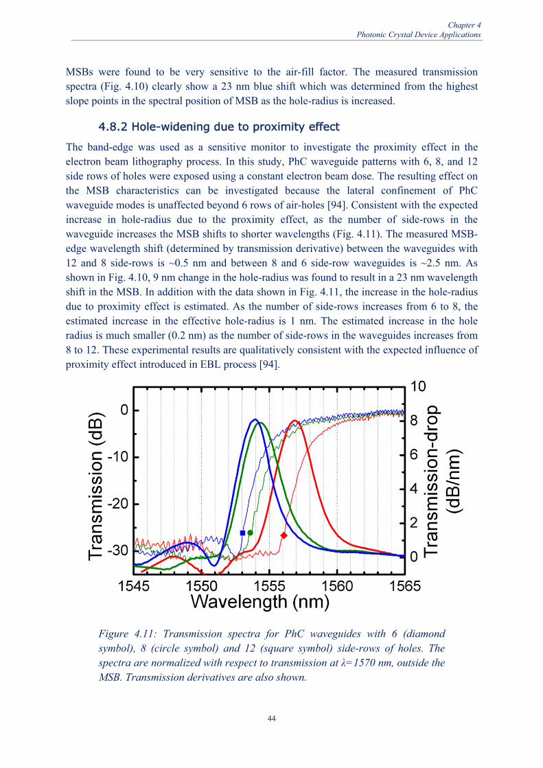
44
Chapter 4Photonic Crystal Device Applications
MSBs were found to be very sensitive to the air-fill factor. The measured transmission spectra (Fig. 4.10) clearly show a 23 nm blue shift which was determined from the highest slope points in the spectral position of MSB as the hole-radius is increased.
4.8.2 Hole-widening due to proximity effect
The band-edge was used as a sensitive monitor to investigate the proximity effect in the electron beam lithography process. In this study, PhC waveguide patterns with 6, 8, and 12 side rows of holes were exposed using a constant electron beam dose. The resulting effect on the MSB characteristics can be investigated because the lateral confinement of PhC waveguide modes is unaffected beyond 6 rows of air-holes [94]. Consistent with the expected increase in hole-radius due to the proximity effect, as the number of side-rows in the waveguide increases the MSB shifts to shorter wavelengths (Fig. 4.11). The measured MSB-edge wavelength shift (determined by transmission derivative) between the waveguides with 12 and 8 side-rows is ~0.5 nm and between 8 and 6 side-row waveguides is ~2.5 nm. As shown in Fig. 4.10, 9 nm change in the hole-radius was found to result in a 23 nm wavelength shift in the MSB. In addition with the data shown in Fig. 4.11, the increase in the hole-radius due to proximity effect is estimated. As the number of side-rows increases from 6 to 8, the estimated increase in the effective hole-radius is 1 nm. The estimated increase in the hole radius is much smaller (0.2 nm) as the number of side-rows in the waveguides increases from 8 to 12. These experimental results are qualitatively consistent with the expected influence of proximity effect introduced in EBL process [94].
Figure 4.11: Transmission spectra for PhC waveguides with 6 (diamond symbol), 8 (circle symbol) and 12 (square symbol) side-rows of holes. The spectra are normalized with respect to transmission at λ=1570 nm, outside the MSB. Transmission derivatives are also shown.

45
Chapter 4Photonic Crystal Device Applications
4.8.3 Waveguide line-defect width
The change of line-defect width is identified to be the most appropriate way as it offers a wide MSB wavelength tuning range. The defect widths are systematically reduced in steps of 0.1 from exactly 3 missing rows to 2.6 in a triangular lattice with period ‘a’. The period in case of W3 and W2.9 are 420 nm. The chosen lattice constants were 440, 450 and 460 nm for W2.8, W2.7 and W2.6 respectively. Evolution of the band-edge as a function of photonic crystal (PhC) waveguide width is investigated in paper E.
Figure 4.12: Measured Transmission spectra (normalized) for W3 to W2.6 PhC waveguides. Normalization is performed with respect to transmission level outside MSB.
Figure 4.12 shows the transmission spectra of the W3 to W2.6. The characteristic dips in transmission from the MSB are visible and the transmission extinction ratios are more than 20 dB for all the waveguides measured. The MSB widths are similar for the different waveguides except for W2.6 waveguide, which shows a slightly wider transmission gap. This could be due to an increase in the coupling strength and dispersion effects. The mode coupling condition for the occurrence of MSB is applicable for a large range of normalized frequency inside photonic band gap. A maximum frequency shift of ∆u=2.82×10⁻² is demonstrated by varying the width of the waveguide. By choosing a lattice constant of 420 nm the corresponding shift of 137 nm is obtained for the operating wavelength. Thus, varying the line-defect width is an efficient way to adjust position of MSB over a large wavelength range.
0.275 0.28 0.285 0.29 0.295 0.3 0.305 0.31 0.315-30
-25
-20
-15
-10
-5
0
5
Normalized Frequency (u)
Tra
nsm
issi
on (
dB)
W2.8 MSB W2.7 MSB W2.6 MSB
W2.936 MSB
W3 MSB

46
Chapter 4Photonic Crystal Device Applications
4.9 Heterostructure PhC waveguiudes
In the otherwise periodic structure engineering defects has been very effectively used for waveguides [31]. Recently, a new class of photonic crystal components/structures have emerged which are PhC heterostructures [20]. Similar to semiconductors heterostructures, photonic heterostructures are composed of two photonic crystals with different band-gaps obtained by changing the air-fill factor (f) or by the lattice constant (a). Photonic crystal heterostructures were experimentally investigated for ~W3 guides and the results are presented in the following sections.
4.9.1 Junction-type PhC waveguides (JPCW)
The experimentally determined wavelength tunability of the MSB by changing the line-defect widths, described in section 4.9.3 can be utilized to design junction-type waveguides to obtain functions such as (relatively) narrow notch and band-pass filters. Junction-type PhC waveguide (JPCW) was realized by juxtaposing W3 and W2.936 for each being a 60 period long PhC waveguide. Figure 4.13 shows a SEM image of the fabricated JPCW at the junction region; the change in the waveguide width is difficult to distinguish owing to fact that the waveguide width shown in right half part of the image is narrower by only ~20 nm.
Figure 4.13 SEM top view of a fabricated JPCW at the junction region. The location of the junction is indicated by a vertical line.
Optical transmission characteristics of JPCWs are very sensitive to change in waveguide width. Figure 4.14 shows the measured transmission spectra of JPCW highlighting two characteristic dips in transmission due to the MSB effect. Elevated transmission peak between two MSBs is evident with the FWHM of 5.6 nm. At the peak, transmission is attenuated only by ~5 dB as compared to power level outside MSB. The peak transmission level between two MSBs is slightly lower than outside MSBs due to small overlap between two MSBs. Spectral sensitivity of this narrow band-pass (FWHM 5.6 nm) filter is presented in paper E. This filter can be used as course WDM filtering [95] and also for selecting desired portion of the spectrum from broad-band spontaneous emission sources.

47
Chapter 4Photonic Crystal Device Applications
Figure 4.14: Normalized transmission spectrum for JPCWs.
4.9.2 Heterostructure W3 (HW3) PhC waveguide
Tunability of MSB position inside photonic band gap is applied in a heterostructure W3 (HW3) PhC waveguide in order to demonstrate novel filters. The HW3 PhC waveguide with a single junction air fill factor results in different filter shapes ranging from resonance-like to wide band pass filters with high transmission which is demonstrated in paper F. Figure 4.15 shows a SEM image of a typical fabricated HW3 PhC waveguide for largest ∆f at the junction; the difference in hole-diameter is clear. The designed air-fill factor difference, ∆f, is 3%, 5% and 13%.
Figure 4.15:The change in the air fill factor (same period) is visible at the junction of the HW3 PhC waveguide. The change in ‘f’ is the maximum with a designed value ∆f=13%.
Figure 4.16 shows the measured transmission spectra for HW3 PhC waveguides where the characteristic dips in transmission due to the MSB effect are visible. Evidently, the occurrence of MSB inside photonic band gap depends on the air-fill factor of PhC. In each spectrum of Fig. 4.16, transmission dip towards shorter wavelength corresponds to a relative

48
Chapter 4Photonic Crystal Device Applications
higher f. Figure 4.16(a) demonstrates a flat transmission level for a broadband between two MSBs with 3 dB bandwidth 65 nm. Only a part of MSB for highest f is visible due to the limited wavelength range of the tunable laser. The designed ∆f = 13% is largest as it is most distinguishable in Fig. 4.15. A slightly lower level of peak transmission in case of HW3 PhC waveguide with ∆f = 5% (Fig. 4.16(b)) is due to the overlap of two MSB cut off at slightly lower transmission level compared to the outside MSB. For a given wavelength, 4th order mode from the first half has to couple back to the fundamental mode in the second half of the HW3 waveguide because of different mode coupling conditions. Similarly, the PhC waveguide fundamental mode, unlike ridge waveguide fundamental mode, couples energy to the 4th order mode in the second half of HW3 when the contra-direction coupling condition is satisfied. The MSB band-edges in HW3 behave in the same manner as in the single W3 waveguide.
The tunability in the position of MSB by altering f is applied to have three different filter shapes. A resonance–like peak with FWHM 3.4 nm is obtained between two stop-bands by having ∆f=3% (Fig. 4.16(c)). In a W3, FWHM of the transmission-dip is broad and an approach based on band-edge was adopted for detection purpose. On the contrary, this HW3 shows a sufficiently sharp transmission peak where the detection of peak wavelength is straightforward therefore the device could potentially be interesting for sensing application.
Figure 4.16: Measured transmission spectra (normalized) for HW3 PhC waveguide for designed (a) ∆f=13% (b) ∆f=5% and (c) ∆f=3%.
The converse symmetries about the junction are also fabricated in order to investigate asymmetric effect owing to the precedence of one particular air-fill factor. Precedence of any of the lower or higher ‘f’ has no influence on transmission characteristics of the waveguide. HW3 refers to both symmetries of the two air fill factor inside the waveguide as the measured characteristics (Fig. 4.16) do not change with reversing the order of the two sections.

49
Chapter 4Photonic Crystal Device Applications
Moreover, as expected for linear systems, transmission characteristics are identical for both juxtapositions i.e., W3 to W2.936 or W2.936 to W3 in JPCWs.
4.10 Temperature tuning of photonic crystal waveguides
In order to demonstrate temperature tuning, the sample is fixed onto a metallic holder which is mounted to a grooved plate. The Peltier element was inserted between the sample mounting and piezoelectric nano-positioning stage. The Peltier effect is used for heating (or cooling) the sample. The temperature of the outer sides of the Peltier element depends on the voltage applied. An NTC (negative temperature coefficient thermistor) is mounted to the bottom of the sample holder and is used to control the temperature of the top-side of the Peltier element, therefore controlling the temperature of the sample. A schematic of the modified setup is shown in figure 4.17. The temperature was varied from 15 to 80 °C.
Figure 4.17: Schematic of the modified sample stage for temperature tuning.
The spectral sensitivity of the MSB to refractive index changes was applied to determine the temperature dependence of the refractive index of the waveguide material [96]. In this work, temperature tuning was demonstrated using the ultrasharp band-edge and the results are presented in paper D (Fig. 4.18(a)), and, the temperature dependence of the narrow transmission peak (Fig. 4.18(b)) of JPCW was presented in paper E. A systematic redshift in the MSB with temperature was observed (Fig. 4.18). The data obtained from both type of devices determined temperature coefficient ∆λ/∆T = 0.1 nm/°C and represented in Fig.

50
Chapter 4Photonic Crystal Device Applications
4.18(c). These result shows potential applications as tunable filters based on the thermal optical adjustment.
Figure 4.18: (a) Ultrasharp band-edge shift with temperature. (b) Temperature dependence of JPCW peak position. (c) Shift of band-edge and JPCW position as a function of temperature.
4.11 Reliability of PhC waveguides
Reliability of PhC structures present great challenge to transfer this promising technology into the domain of commercial applications. In order to address this issue, the systematic evaluation of the optical transmission characteristics of a set of PhC waveguides (PhCWs) was done. The optimized hole-reshaping process was applied to the fabrication of several PhCWs with a lattice constant a=420 nm. To assess the process reliability for different structural parameters, two air filling factors with a designed difference of 9 nm in their hole-radii were fabricated. These devices and their corresponding transmission spectra are labelled from A to I. The set of devices from A to D and E to I have two different air-fill factors f1=40% and f2=45%, respectively. The minimum number of side rows is 6 as the lateral confinement of PhC waveguide modes is unaffected beyond 6 rows of air-holes [94]. Figure 4.19 shows the measured transmission spectra of the PhC waveguides in which the etched holes have been reshaped. All the devices show a consistent transmission drop of 30-35 dB with a bandwidth of ~12 nm. Similarly, all devices show sharp band-edges with ~30 dB

51
Chapter 4Photonic Crystal Device Applications
transmission drop within 4 nm change in the wavelength. Devices A to D have same air fill factor and only differ in the number of side rows. The small variation in the position of MSB in these devices is due to a small increase in the hole-diameter due to proximity effect in EBL process [56, 94]. Devices B and C are identical in all parameters and hence the same spectral shape in transmission are well reproduced. Devices E to I have higher air fill factor f2 and also present consistent spectral shapes. Irrespective of the air fill factors, the measured spectral shapes (attenuation, band-width, transmission band edges) for the different waveguides are almost identical. The spectral characteristics of the transmission MSB in identical waveguides show that the reliability, in terms of spectral position and shape, of fabricated PhCWs using the hole reshaping process is significantly improved. A systematic one-to-one comparison is made with as-etched (without MT) devices and the results are presented in paper G.
Figure 4.19: Transmission spectra for a series of PhC waveguides with cylindrical holes for two different air fill factors f1=40% and f2=45%). The spectra are normalized with respect to transmission at λ=1500 nm, outside the MSB.

52
CHAPTER5CONCLUSIONSANDOUTLOOK
In summary, the design, fabrication and characterization of PhC components in the InP-based material system highlighting several functional elements such as waveguides, mirrors, filters and resonators, has been the focus of this thesis and the state-of-the-art fabrication scheme has been implemented in the PhC devices.
5.1 Fabrication of PhC structures
From the perspective of fabrication, a novel post-etch process based on so-called mass-transport (MT) has been demonstrated for the first time on InP-based PhC. Mass transport smoothens and effectively reduces imperfections in PhCs which are introduced at the pattern transfer steps. The reshaping of etched PhC to achieve vertical side-walls can be used to counter very deep etching requirement. The fabricated W3 InP based waveguides have the best-to-date reported spectral characteristics of mini-stop band notch filters. The reliability analysis was done for several MSB PhC (W3) waveguide devices, identical in all aspects except that they were fabricated by two schemes: as-etched and by using the MT method. A statistical analysis of several devices fabricated by MT process technology shows a clear improvement in the reliability of optical transmission characteristics. The novel post-etch process step based on MT technology could be beneficial in reducing the etch-induced damage rendering it very promising for achieving high optical quality in PhC components. The investigation of the carrier recombination lifetimes of the healed nanostructures will be interesting for future studies. Material reflow in MT process depends on the annealing temperature and duration, on the as-etched profile, and on the material composition at the surface. A detailed study of the effect of these parameters on the resulting hole shape are necessary to take full advantage of this process. Although this thesis focuses on MT technology for InP PhCs it was proposed that other materials and other types of nanostructures could benefit from this method. Such an approach has been recently demonstrated for GaAs-based nanostructures [97].
InP-based suspended membranes represent another technology platform for 2D PhCs. A primary advantage of this platform is lower optical loss compared to substrate-type material system. In the course of this work, InGaAsP suspended membrane technology was

53
Chapter 5Conclusions and outlook
developed. An H2 cavity with a linewidth of ~0.4 nm, corresponding to a Q value of ~3675 has been shown. The performance of these cavities can be improved using the MT technology especially to improve side wall verticality of ICP etched PhC holes. In addition, it is interesting to investigate MT technology for carrier lifetime engineering in such membrane type PhC cavities for switching (short carrier life times) and for low threshold lasers (long carrier lifetimes).
5.2 Device applications of PhCs
Polarization dependent property of a PhC mirror was used to separate the TE and TM states in a polarization beam splitter (PBS). An ultra-compact PBS was fabricated by combining a multimode waveguide with internal PhC, having a band gap only for TE polarization while it is absent for the other. By suitably placing such a PhC structure in the multimode section of the multimode interference (MMI) coupler, the reflected TE, and the transmitted TM could be collected by the respective output ports of MMI. The optimisation of the structure, for example by two step lithography one for defining the MMI and other for PhC, can enhance the performance of PBS further.
The phenomena of MSBs in different types of PhC waveguides and its potential applications for filtering, tuning and sensing have been investigated. A method enabling spectral tuning with sub-nanometer accuracy based on the transmission MSB has been demonstrated. Excellent spectral characteristics showing high attenuation (~30 dB) and ultrasharp cut-offs (transmission-drop of 8.2 dB/nm) are obtained in 50 μm long W3 PhC waveguides wherein the etched holes were reshaped through the use of MT technology. Similarly, MSBs in broad enough PhC waveguides that operated in the multimode regime were investigated by varying the waveguide width in incremental amounts (fraction of the lattice constant). This approach was shown to be an efficient way to tune the position of the MSB in wavelength without having to increase the air-fill factor.
Analogous to semiconductors heterostructures, photonic heterostructures are composed of two PhCs with different band gaps obtained either by changing the air-fill factor or by the lattice constant. Juxtaposing two PhCs and the use of heterostructures in waveguide geometry has been experimentally investigated in this thesis work. In particular, multimode line defect waveguides with internal MSB brought a new dimension, both for fundamental physics and for applications. MSBs in heterostructure waveguides have shown interesting applications such as designable band-pass flat-top filters, and resonance-like filters with high transmission. A single junction-type photonic crystal waveguide (JPCW), comprising of distinct combinations of two line defect waveguides, differing by ~20 nm in the widths, was fabricated. A narrow band pass filter realized using this concept has a FWHM of 5.6 nm and a high transmission (~20 dB above the signal level corresponding to the MSBs). Tunability of MSB position inside photonic band gap is applied in a heterostructure W3 (HW3) PhC waveguide in order to demonstrate novel filters. Different filter shapes ranging from resonance-like to wide band pass filters with high transmission are demonstrated in HW3 PhC waveguide. By altering the position and/or engineering the junction in the JPCW and HW3 and cascading to form multi-junction waveguides, efficient wide bandstop filters and narrow

54
Chapter 5Conclusions and outlook
bandpass filters can be obtained. Similarly, careful cascading of the PhC waveguides can be used to tailor the filter characteristics further.
Disordered photonic crystal waveguides with lithographically controlled amount of disorder provides a powerful way of enhancing the interaction between light and matter [27]. Although the present work addresses abrupt junctions PhC waveguides, the study of disorder and chirping in these guides can be an interesting direction for the future continuation of this work.

55
CHAPTER6GUIDETOTHEPAPERS
PAPER A: N. SHAHID, S. NAUREEN, M. Y. LI, M. SWILLO AND S. ANAND, “NOVEL POSTETCH
PROCESS TO REALIZE HIGH QUALITY PHOTONIC CRYSTALS IN INP,” J. VAC. SCI. TECHNOL. B
29, 031202 (2011).
In this paper, thermally driven reflow of material during annealing was used to obtain near-vertical sidewall profiles for high-aspect-ratio nanostructures in InP fabricated by dry etching. Nearly cylindrical profiles were obtained for high-aspect-ratio PhC holes with diameters as small as 200-350 nm. For the first time, a novel post-etch process based on so-called mass-transport (MT) technology was demonstrated for substrate-type InP-based PhC.
Author Contribution: Part in FDTD and PWE simulations, sample fabrication (design, EBL, PECVD, RIE and CAIBE), device processing (cleaving and lapping), end-fire measurements, data analysis and writing of the paper.
PAPER B: Y. SHI, N. SHAHID, M. Y. LI, A. BERRIER, S. HE AND S. ANAND, “EXPERIMENTAL
DEMONSTRATION OF AN ULTRACOMPACT POLARIZATION BEAMSPLITTER BASED ON A
MULTIMODE INTERFERENCE COUPLER WITH INTERNAL PHOTONIC CRYSTALS,” OPTICAL
ENGINEERING 49, 060503 (2010).
The fabrication and characterization of a compact InP-based polarization beam splitter (PBS) is presented in this paper. A multimode interference (MMI) coupler with an internal air hole photonic crystal (PhC) section is utilized to separate the two polarizations. The PhC structure in the middle of the MMI is polarization dependent, so that one polarization is reflected and the other one is transmitted; both are collected by the respective output ports of the MMI coupler. The obtained experimental results show that the PBS as short as ~400 μm has an extinction ratio as large as 15 dB.
Author Contribution: Device processing (cleaving and lapping), end-fire characterization, data analysis, and part in writing of the paper.

56
Chapter 6Guide to the papers
PAPER C: NAEEM SHAHID, SHAGUFTA NAUREEN, MING-YU LI, MARCIN SWILLO AND
SRINIVASAN ANAND, “HIGH QUALITY PHOTONIC CRYSTAL WAVEGUIDE FILTERS BASED ON
MODE-GAP EFFECT,” 23RD INTERNATIONAL CONFERENCE ON INDIUM PHOSPHIDE AND
RELATED MATERIALS – IPRM 2011, MAY 22-26, 2011, BERLIN, GERMANY.
This paper demonstrates that the depth and shape irregularities, which are inherent in the etching process of high-aspect-ratio 2D PhCs in InP-based materials have a detrimental effect on the spectral characteristics of ministop-bands (MSBs) which are due to coupling of the higher-order modes with the fundamental mode. The high optical quality filters based on the MSB effect have been demonstrated. The MSBs transmission spectrum shows well behaved cut-offs for reshaped PhC waveguides.
Author Contribution: Design and fabrication, end-fire characterization, writing of the paper.
PAPER D: N. SHAHID, N. SPEIJCKEN, S. NAUREEN, M. Y. LI, M. SWILLO AND S. ANAND, “ULTRASHARP MINISTOP-BAND EDGE FOR SUBNANOMETER TUNING RESOLUTION,” APPL. PHYS. LETT. 98, 0811121 (2011).
This paper proposes and demonstrates a method that enables spectral tuning with sub-nanometer accuracy, and is based on the transmission mini-stop band (MSB) in line-defect multimode PhC waveguides. The fabricated MSB filter has ultra-sharp edges which show a 30 dB drop in transmission in a 4 nm wavelength span. The use of the ultra-sharp MSB edge to (optically) determine PhC fabrication accuracy is demonstrated. The wavelength position of the MSB could be tuned by temperature, with a coefficient of 0.1 nm/˚C. The spectral characteristics of the MSB realized in this work are promising for sensing, tuning and modulation applications.
Author Contribution: Part in FDTD and PWE simulations, sample fabrication (design, EBL, PECVD, RIE and CAIBE), device processing (cleaving and lapping), end-fire characterization, data analysis, and writing of the paper.
PAPER E: N. SHAHID, M. AMIN, S. NAUREEN, M. SWILLO AND S. ANAND, “JUNCTION-TYPE
PHOTONIC CRYSTAL WAVEGUIDES FOR NOTCH- AND PASS-BAND FILTERING,” OPT. EXPRESS
VOL. 19, NO. 21, 21074 (2011).
Evolution of the mode gap and the associated transmission mini-stop band (MSB) as a function of PhC waveguide width is theoretically and experimentally investigated in this paper. The change of line-defect width is identified to be the most appropriate way since it offers a wide MSB wavelength tuning range. A high transmission narrow-band filter is experimentally demonstrated in a junction-type waveguide composed of two PhC waveguides with slightly different widths. The FWHM is 5.6 nm; the peak transmission is attenuated by only ~5 dB and is ~20 dB above the MSBs. Additionally, temperature tuning of the filter were also performed. The results show red-shift of the transmission peak and the MSB edges with a gradient of dλ/dT=0.1 nm/˚C. It is proposed that the transmission MSBs in such junction-type cascaded PhC waveguides can be used to obtain different types of filters.

57
Chapter 6Guide to the papers
Author Contribution: Part in FDTD and PWE simulations, sample fabrication (design, EBL, PECVD, RIE and CAIBE), device processing (cleaving), end-fire characterization, data analysis, and writing of the paper.
PAPER F: N. SHAHID, M. AMIN, S. NAUREEN AND S. ANAND, “ MINI-STOP BANDS IN SINGLE
HETEROJUNCTION PHOTONIC CRYSTAL WAVEGUIDES,” SUBMITTED TO APPL. PHYS. LETT.
Spectral characteristics of MSBs in line-defect heterostructure PhC waveguides (HPCWs) having one abrupt interface are investigated in this paper. Tunability of the MSB position by air-fill factor is utilized to demonstrate different filter functions ranging from resonance-like to wide band pass filters with high transmission. The narrowest filter realized has a resonance-like transmission peak with a full width at half maximum of 3.4 nm. These devices could be attractive for course wavelength selection (pass and drop) and sensing applications. Sensitivity of resonance-like high transmission peak obtained by overlapping of two MSBs can positively be used for sensing applications. By engineering the interface, for example by band-gap grading, optical properties can be further improved.
Author Contribution: Part in FDTD and PWE simulations, sample fabrication (design, EBL, PECVD, RIE and CAIBE), device processing (cleaving), end-fire characterization, data analysis, and writing of the paper.
PAPER G: NAEEM SHAHID, SHAGUFTA NAUREEN AND SRINIVASAN ANAND, “EFFECT OF HOLE
SHAPES ON THE RELIABILITY OF DEEPLY-ETCHED INP-BASED PHOTONIC CRYSTAL DEVICES,”
PHYS. STATUS SOLIDI C 9, NO. 7, 1670–1673 (2012).
This paper presents systematic evaluation of the optical transmission characteristics of a set of PhC waveguides fabricated by two schemes. An optimized hole-reshaping process to obtain cylindrical holes was applied in one scheme and a comparison is made with as-etched PhCWs. The spectral characteristics of the transmission mini-stopband (MSB) in identical waveguides show that the reliability, in terms of spectral position and shape, of fabricated PhCWs using the hole reshaping process is significantly improved in comparison to the as-etched waveguides. The obtained MSB characteristics are attractive for coarse WDM filtering and wavelength selective mirrors.
Author Contribution: Sample fabrication (design, EBL, PECVD, RIE and CAIBE), device processing (cleaving and lapping), end-fire characterization, data analysis, and writing of the paper.

58
BIBLIOGRAPHY
[ 1 ] “The EU framework Programme for Research and Innovation,” (2011), URL www.ec.europa.eu/research/horizon2020.
[2] “A European roadmap for photonics and nanotechnologies,” (2008), URL www.ist-mona.org.
[3] E. Yablonovitch and T. Gmitter, “Photonic band structure: the face-centered-cubic case,” Phys. Rev. Lett. 63, 1950 (1989).
[4] E. Yablonovitch and T. Gmitter, “Inhibited spontaneous emission in solid state physics and electronics,” Phys. Rev. Lett. 58, 2059 (1987).
[5] S. John, “Strong localization of photons in certain disordered dielectric superlattices,” Phys. Rev. Lett. 58, 2486 (1987).
[6] T. F. Krauss, R. M. De La Rue and S. Brand, "Two-dimensional photonic-band gap structures operating at near infrared wavelengths" Nature 383, 699-702 (1996).
[ 7 ] M. Loncar, D. Nedeljkovic, T. Doll, J. Vuckovic, A. Scherer and T. P Pearsall, “Waveguiding in planar photonic-crystals,” Appl. Phys. Lett. 77 (13), 1937-1939 (2000).
[8] T. Baba, N. Fukaya and J. Yonekura, “Observation of light transmission in photonic crystal waveguides with bends,” Electron. Lett. 35, 654–655 (1999).
[9] S. Y. Lin, E. Chow, S. G. Johnson and J. D. Joannopoulos, “Demonstration of highly efficient waveguiding in a photonic crystal slab at the 1.5 μm wavelength,” Opt. Lett. 25, 1297–1299 ( 2000).
[10] C. J. Smith, H. Benisty, S. Olivier, M. Rattier, C. Weisbuch, T. F. Krauss, R. M. De La Rue, R. Houdré and U. Oesterle, “Low-loss channel waveguides with two-dimensional photonic crystal boundaries,” Appl. Phys. Lett. 77, 2813–2815 (2000).
[11] M. Notomi, A. Shinya, K. Yamada, J. Takahashi and I. Yokohama, “Single-mode transmission within photonic band gap of width-varied single-line-defect photonic crystal waveguides on SOI substrates,” Electron. Lett. 37, 293–295 (2001).
[12] Y. Sugimoto, N. Ikeda, N. Carlsson, and K. Asakawa, “AlGaAs-based two-dimensional photonic crystal slab with defect waveguides for planar lightwave circuit applications,” IEEE J. Quantum Electron. 38, 760–769 (2002).
[13] O. Painter, R. K. Lee, A. Scherer, A. Yariv, J. D. O’Brien, P. D. Dapkus and I. Kim, “Two-dimensional photonic band-gap defect mode laser,” Science 284 (5421), 1819-1821 (1999).
[14] J. K. Hwang, H. Y. Ryu, D. S. Song, I. Y. Han, H. W. Song, H. K. Park, Y. H. Lee and D. H. Jang, “Room-temperature triangular-lattice two dimensional photonic band gap lasers operating at 1.54 μm,” Appl. Phys. Lett. 76, 2982–2984 (2000).
[15] P. T. Lee, J. R. Cao, S. J. Choi, Z. J. Wei, J. D. O’Brien and P. D. Dapkus, “Room-temperature operation of VCSEL-pumped photonic crystal lasers,” IEEE Photon. Technol. Lett. 14, 435–437 (2002).
[16] C. Monat, C. Seassal, X. Letartre, P. Viktorovitch, P. Regreny, M. Gendry, P. Rojo-Romeo, G. Hollinger, E. Jalaguier, S. Pocas and B. Aspar, “InP 2D photonic crystal

59
microlasers on silicon wafer: room temperature operation at 1.55 μm,” Electron. Lett. 37, 764–765 (2001).
[17] S. Noda, A. Chutinan and M. Imada, “Trapping and emission of photons by a single defect in a photonic band gap structure,” Nature 407(6084), 608–610 (2000).
[18] C. J. M. Smith, R. M. DeLaRue and M. Rattier, “Coupled guide and cavity in a two-dimensional photonic crystal,” Appl. Phys. Lett. 78(11), 1487–1489 (2001).
[19] S. Y. Lin, E. Chow, S. G. Johnson and J. D. Joannopoulos, “Direct measurement of the quality factor in a two-dimensional photonic-crystal microcavity,” Opt. Lett. 26(23), 1903–1905 (2001).
[20] E. Istrate and E. H. Sargent, “Photonic crystal heterostructures and interfaces,” Rev. Mod. Phys. 78, 455-481 (2006).
[21] S. Kocaman, M. S. Aras, D. L. Kwong, A. Stein, P. Hsieh, and C. W. Wong, J. F. McMillan, C. G. Biris, N. C. Panoiu, M. B. Yu, D. L. Kwong, A. Stein and C. W. Wong, “Zero phase delay in negative-refractive-index photonic crystal superlattices,” Nat. Photonics 5, 499–505 (2011).
[22] Photonic crystals and light localization in the 21th century, Editor. C. M. Soukoulis, Nato Science, Series C 563, 351-371 (2002).
[23] T. F. Krauss, “Slow light in photonic crystal waveguides,” J. Phys. D: Appl. Phys. 40, 2666 (2007).
[24] V. Zabelin, L. A. Dunbar, N. Le Thomas, R. Houdré, M. V. Kotlyar, L. O’Faolain and T. F. Krauss, “Self-collimating photonic crystal polarization beam splitter,” Opt. Lett. 32(5), 530–532 (2007).
[25] H. Kosaka, T. Kawashima, A. Tomita, M. Notomi, T. Tamamura, T. Sato and S. Kawakami,” Superprism phenomena in photonic crystals,” Phys. Rev. B 58, R10096 (1998).
[26] A. Berrier, M. Mulot, M. Swillo, M. Qui, L. Thylen, A. Talneau and S. Anand, “Negative refraction at Infrared wavelengths in a two-dimensional photonic crystal” Phys. Rev. Lett. 93, 073902 (2004).
[27] Luca Sapienza, Henri Thyrrestrup, Søren Stobbe, Pedro David Garcia, Stephan Smolka and Peter Lodahl, “Cavity quantum electrodynamics with Anderson-localized modes,” Science 327, 1352-5 (2010).
[28] A. Tandaechanurat, S. Ishida, D. Guimard, M. Nomura, S. Iwamoto and Y. Arakawa, “Lasing oscillation in a three-dimensional photonic crystal nanocavity with a complete band gap,” Nat. Photonics 5, 91-94 (2011).
[29] S. Noda, K. Tomoda, N. Yamamoto and A. Chutinan, “Full three dimensional photonic band gap crystals at near-infrared wavelength,” Science 289, 604-606 (2000).
[30] J. E. G. J. Wijnhoven and W. L. Vos, “Preparation of photonic crystals made of air spheres in titania,” Science 281, 802- 804 (1998).
[31] L. Thylén, M. Qiu and S. Anand, “Photonic Crystals—A Step towards Integrated Circuits for Photonics”. ChemPhysChem 5(9), 1268-1283 (2004).
[32] A. Berrier, M. Mulot, S. Anand, A Talneau, R. Ferrini and R. Houdré, “Characterization of the feature-size dependence in Ar/Cl2 chemically assisted ion beam etching of InP-based photonic crystals devices,” J. Vac. Sci. Technol. B 25(1), 1 (2007).

60
[33] J. F. Holzman, P. Strasser, R. Wüest, F. Robin, D. Erni and H. Jäckel, “Ultrafast carrier dynamics in InP photonic crystals,” Nanotechnology 16, 949 (2005).
[34] A. Berrier, Y. Shi, J. Seigert, S. Marcinkevicius, S. He and S. Anand, “Accumulated sidewall damage in dry etched photonic crystals,” J. Vac. Sci. Technol. B 27(4), 1969-1975 (2009).
[35] Y. Shi, D. Dai and S. He, “Proposal for an ultra-compact polarization beam splitter based on a photonic-crystal-assisted multimode interfer- ence coupler,” IEEE Photon. Technol. Lett. 19, 825–827 (2007).
[36] T. Y. L. Ang and M. K. Chin, “The effects of periodic and quasi-periodic orders on the photonic band gap structures of microring coupled-resonator optical waveguides,” Opt. Express 17, 5176 (2009).
[37] S. Inoue and S. Yokoyama, “Enhancement of two-photon excited fluorescence in two-dimensional nonlinear optical polymer photonic crystal waveguides,”Appl Phys. Lett. 93, 111110 (2008).
[38] Y. Zhang, Z. J. Li and B. J. Li, “Multimode interference effect and self-imaging principle in two-dimensional silicon photonic crystal waveguides for terahertz waves,” Opt. Express 14, 2679–2689 (2006).
[39] S. Olivier, M. Rattier, H. Benisty, C. J. M. Smith, R. M. De La Rue, T. F. Krauss, U. Oesterle, R. Houdré and C. Weisbuch, “Mini-stopbands of a one-dimensional system: The channel waveguide in a two-dimensional photonic crystal,” Phys. Rev. B 63, 113311 (2001).
[40] T. Cao, M. J. Cryan, P. S. Ivanov, D. Ho, B. Ren, I. J. Craddock, J. M. Rorison and C. J. Railton, “Modeling of chirped pulse propagation through a mini-stop band in a two-dimensional photonic crystal waveguide,” J. Opt. Soc. Am. B 24, 1575 (2007).
[41] M. Ayre, C. Cambournac, O. Khayam, H. Benisty, T. Stomeo and T. F. Krauss, “Photonic crystal waveguides for coarse-selectivity devices,” Photonics Nanostruct. Fundam. Appl. 6(1), 19-25 (2008).
[42] S. A. Moore, L. O'Faolain, T. P. White and T. F. Krauss, “Photonic crystal laser with mode selective mirrors,”Opt. Express 16(2), 1365-1370 (2008).
[43] L. Cao, Y. Huang, X. Mao, F. Li, W. Zhang and J. Peng, “Fluid Sensor Based on Transmission Dip Caused by Mini-stop band in Photonic Crystal Slab,” Chin. Phys. Lett. 25(1), 2101 (2008).
[44] Yoshihiro Akahane, Takashi Asano, Bong-Shik Song and Susumu Noda, “High-Q photonic nanocavity in a two-dimensional photonic crystal,” Nature 425, 944-947 (2003).
[45] Jan Hendrik Wülbern, Jan Hampe, Alexander Petrov, Manfred Eich, Jingdong Luo, Alex K.-Y. Jen, Andrea Di Falco, Thomas F. Krauss and Jürgen Bruns ”Electro-optic modulation in slotted resonant photonic crystal heterostructures,” Appl. Phys. Lett. 94, 241107 (2009).
[46] A. Di Falco, L. O’Faolain and T. F. Krauss “Chemical sensing in slotted photonic crystal heterostructure cavities” Appl. Phys. Lett. 94, 063503 (2009).
[47] S. Noda, “Photonic crystal lasers—ultimate nanolasers and broad area coherent lasers,” J. Opt. Soc. Am. B 27, B1–B8 (2010).
[48] Photonic Crystals: Molding The Flow Of Light (Second Edition), John D. Joannopoulos, Steven G. Johnson, Joshua N. Winn, Robert D. Meade, Princeton University Press (2008).

61
[49] K. Busch and S. John, “Photonic band gap formation in certain self-organizing systems,” Phys. Rev. E 58(3), 3896–3908 (1998).
[50] G. Floquet, “Sur les équations différentielles linéaires à coefficients périodiques,” Ann. Ecole Norm. Sér. 2(12), 47–89 (1883).
[51] F. Bloch, “Über die Quantenmechanik der Electronen in Kristallgittern,” Z. Phys. 52, 555–600 (1928).
[52] S. G. Johnson and J. D Joannopoulos, “Block-iterative frequency-domain methods for Maxwell’s equations in a planewave basis,” Opt. Express 8, 173 (2001).
[53] R. D. Meade, K. D. Brommer, A. M. Rappe and J. D. Joannopoulos, “Photonic bound states in periodic dielectric materials," Phys. Rev. B 44, 13 772 (1991).
[54] K. S. Yee, “Numerical solution of initial boundary value problems involving Maxwell's equations in isotropic media," IEEE Trans. Antennas Propagat. 14(8), 302 (1966).
[55] M. Qiu, B. Jaskorzynska, M. Swillo and H. Benisty, “Time-domain 2D modeling of slab-waveguide based photonic-crystal devices in the presence of radiation losses,” Microwave Opt. Technol. Lett. 34, 387 (2002).
[56] N. Shahid, N. Speijcken, S. Naureen, M. Y. Li, M. Swillo, and S. Anand, “Ultrasharp ministop-band edge for subnanometer tuning resolution,” Appl. Phys. Lett. 98, 0811121 (2011).
[57] F. Pommereau, L. Legouezigou, S. Hubert, S. Sainson, J. P. Chan- douineau, S. Fabre, G. H. Duan, B. Lombardet, R. Ferrini and R. Houdre, “Fabrication of low loss two-dimensional InP photonic crystals by inductively coupled plasma etching,” J. Appl. Phys. 95(5), 2242–45 (2004).
[ 58 ] P. Rai-Choudhury, Handbook of Microlithography, Micromachining and Microfabrication. Vol. 1 Microlithography (SPIE, 1997).
[59] H. W. Lehmann and R. Widmer, “Profile control by reactive sputter etching,”J. Vac. Sci. Technol. 15 (2), 319-326 (1978).
[60] H. W. Lehmann and R. Widmer. “Fabrication of deep square wave structures with micron dimensions by reactive sputter etching.” Appl. Phys. Lett. 32 (3), 163-165 (1978).
[61] S. Matsuo, ”Selective etching of SiO2 relative to Si by plasma reactive sputter etching,” J. Vac. Sci. Technol. 17 (2), 587-594 (1980).
[62] B. A. Raby, “Mass spectroscopy study of plasma etching,” J. Vac. Sci. Technol. 15 (2), 205-208 (1978).
[63] L. Gatilova, S. Bouchoule, S. Guilet and P Chabert, “Investigation of InP etching mechanisms in a Cl2/H2 inductively coupled plasma (ICP) by optical emission spectroscopy,” J. Vac. Sci. Technol A. 27 (1), 262 (2009).
[64] Bryan Ellis, Marie A. Mayer, Gary Shambat, Tomas Sarmiento, James Harris, Eugene E. Haller and Jelena Vučković. “Ultralow-threshold electrically pumped quantum-dot photonic-crystal nanocavity laser,” Nature Photon. 5, 297-300 (2011).
[65] Min-Kyo Seo, Hong-Gyu Park, Jin-Kyu Yang, Ju-Young Kim, Se-Heon Kim and Yong-Hee Lee, “Controlled sub-nanometer tuning of photonic crystal resonator by carbonaceous nano-dots,” Opt. Express 16 (13), 9829-9837, (2008).

62
[66] Huang Jingqing, Se-heon Kim, Jonathan Gardner, Philippe Regreny, Christian Seassal, Pablo Aitor Postigo and Axel Scherer, “Room temperature , continuous-wave coupled-cavity InAsP / InP photonic crystal laser with enhanced far-field emission directionality,”Appl. Phys. Let. 99, 091110, (2011).
[67] Mehmet A. Dündar, Els C. I. Ryckebosch, Richard Nötzel Fouad Karouta, Leo J. van IJzendoorn, and Rob W. van der Heijden, “Sensitivities of InGaAsP photonic crystal membrane nanocavities to hole refractive index,” Opt. Express 18(5), 4049-4056, (2010).
[68] Iwamoto Satoshi, Yasuhiko Arakawa and Akiko Gomyo, “Observation of enhanced photoluminescence from silicon photonic crystal nanocavity at room temperature,” Appl. Phys. Lett. 91, 211104 (2007).
[69] Han-Youl Ryu, Masaya Notomi, Yong-Hee Lee, Guk-Hyun Kim and G. Hugh Song, “High-Q whispering-gallery mode in the photonic crystal hexagonal cavity,” Proceedings of SPIE 5356 (2004).
[70] Z. L. Liau and J. N. Walpole, paper WB3, Technical Digest, Topical meeting on integrated and guide-wave optics, Opt. Soc. America (1982).
[ 71 ] Z. L. Liau and J. N. Walpole, “A novel technique for GaInAsP/InP buried heterostructure laser fabrication,”Appl. Phys. Lett. 40, 568 (1982).
[72] Z. L. Liau, J. N. Walpole and D. Z. Tsang, “Low threshold GaInAsP/InP buried heterostructure lasers with a chemically etched and mass transported mirror,” Appl. Phys. Lett. 44, 945 (1984).
[73] M. Aybe, H. Nagasawa and K. Kaneko, “Vapor-phase transport of GaAs on a V-shape grooved GaAs substrate,” J. Cryst. Growth 58, 180-184 (1982).
[74] Z. L. Liau, V. Diadiuk, J. N. Walpole and D. E. Mull, “Gallium phosphide microlenses by mass transport,” Appl. Phys. Lett. 55, 97 (1989).
[75] Z. L. Liau and J. N. Walpole, “Surface-emitting GaInAsP/InP laser with low threshold current and high efficiency” Appl. Phys. Lett. 46(2), 115 (1985).
[76] Z. L. Liau, V. Diadiuk, J. N. Walpole and D. E. Mull, “Large-numerical-aperture InP lenslets by mass transport” Appl. Phys. Lett. 52, 1859 (1988).
[ 77 ] T. Inoue, S. Nakajima, Y. Luo, T. Oki, H. Iwaoka, Y. Nakano and K. Tada, “InGaAsP/InP Gain-Coupled Distributed Feedback Laser with a Corrugated Active Layer,” Jpn. J. Appl. Phys. 30, L1808-L1810 (1991).
[78] Z. L. Liau and H. J. Zeiger, “Surface-energy-induced mass-transport phenomenon in annealing of etched compound semiconductor structures: Theoretical modeling and experimental confirmation,” J. Appl. Phys. 67(5), 2434 (1990).
[ 79 ] N. Miliou, R. Srivastava and R. V. Ramaswamy, “A 1.3-μm directional coupler polarization splitter by ion exchange,” J. Lightwave Technol. 11(2), 220–225, (1993).
[80] S. Kim, G. P. Nordin, J. Cai and J. Jiang, “Ultracompact high-efficiency polarizing beam splitter with a hybrid photonic crystal and conventional waveguide structure,” Opt. Lett. 28, 2384–2386 (2003).
[81] D. M. Mackie, T. J. Tayag and T. E. Batchman, “Polarization separation/ combination based on self-imaging,” Opt. Eng. 40, 2265– 2272 (2001).

63
[82] H. Benisty, “Modal analysis of optical guides with two-dimensional photonic band-gap boundaries,” J. Appl.Phys. 79, 7483 (1996).
[83] T. Baba, “Slow light in photonic crystals,” Nat. Photonics 2(8), 465–473 (2008).
[ 84 ] M. L. Povinelli, S. G. Johnson and J. D. Joannopoulos, “Slow-light, band-edge waveguides for tunable time delays,” Opt. Express 13(18), 7145–7159 (2005).
[85] E. Schwoob, H. Benisty, C. Weisbuch, C. Cuisin, E. Derouin, O. Drisse, G. H. Duan, L. Legouézigou, O. Legouézigou and F. Pommereau, “Enhanced gain measurement at mode singularities in InP-based photonic crystal waveguides,” Opt. Express 12(8), 1569–1574 (2004).
[86] M. Notomi, K. Yamada, A. Shinya, J. Takahashi, C. Takahashi and I. Yokohama, “Extremely large group- velocity dispersion of line-defect waveguides in photonic crystal slabs,” Phys. Rev. Lett. 87(25), 253902 (2001).
[87] J. Li, T. P. White, L. O’Faolain, A. Gomez-Iglesias and T. F. Krauss, “Systematic design of flat band slow light in photonic crystal waveguides,” Opt. Express 16(9), 6227–6232 (2008).
[88] A. Di Falco, L. O’Faolain and T. F. Krauss, “Dispersion control and slow light in slotted photonic crystal waveguides,” Appl. Phys. Lett. 92(8), 083501 (2008).
[89] T. Baba, A. Motegi, T. Iwai, N. Fukaya, Y. Watanabe and A. Sakai, "Light propagation characteristics of straight single-line-defect waveguides in photonic crystal slabs fabricated into a silicon-on-insulator substrate,", IEEE Journal of Quantum Electron. 38(7), 743-752 (2002).
[90] A. Talneau, M. Mulot, S. Anand, S. Olivier,M. Agio, M. Kafesaki and C.M. Soukoulis, ”Modal behavior of single-line photonic crystal guiding structures on InP substrate,” Photonics and Nanostructures – Fundamentals and Applications 2 1–10 (2004).
[91] M. Davano, A. Xing, J. W. Raring, E. L. Hu and D. J. Blumenthal, “Broadband Notch Filters Based on Quasi-2-D Photonic Crystal Waveguides for InP-Based Monolithic Photonic-Integrated Circuits,” IEEE J. Sel. Top. Quantum Electron. 12(6), 1164 - 1174 (2006).
[92] K. Cui, Y. Huang, G. Zhang, Y. Li, X. Tang, X. Mao, Q. Zhao, W. Zhang and J. Pengllo, “Temperature dependence of mini-stop band in double-slots photonic crystal waveguides,” Appl. Phys. Lett. 95, 191901 (2009).
[93] A. Talneau, I. Sagnes, R. Gabet, Y. Jaouen, and H. Benisty, “Ultrasharp edge filtering in nanotethered photonic wires,” Appl. Phys. Lett. 97, 191115 (2010).
[94] R. Wüest, F. Robin, P. Strasser, H. Jäckel and D. Erni, “Influence of proximity effects in electron-beam lithography on the optical properties of planar photonic-crystal waveguides,” J. Appl. Phys. 102, 083110 (2007).
[ 95 ] K. Ogusu and K Takayama, “Transmission characteristics of photonic crystal waveguides with stubs and their application to optical filters,”Opt. Lett. 32, 2185 (2007).
[96] B. Wild, R. Ferrini, R. Houdré, M. Mulot, S. Anand and C. J. M. Smith, “Temperature tuning of the optical properties of planar photonic crystal microcavities,” Appl. Phys. Lett. 84, 846 (2004).

64
[ 97 ] X. Qian, S. Vangala, D. Wasserman and W. D. Goodhue, “High-optical-quality nanosphere lithographically formed InGaAs quantum dots using molecular beam epitaxy assisted GaAs mass transport and overgrowth.” J. Vac. Sci. Technol. B 28(3), C3C9 (2010).