energy harvesting using rf mems
12
Energy harvesting using RF MEMS Seminar Report Master of Technology In VLSIVLSI & EMBEDDED SYSTEM ENGINEERING By Smarak Tripathy (M.tech 2nd Semester and Roll no. 1459020) School of Electronics Engineering KIIT University April 2015
-
Upload
smarak-tripathy -
Category
Engineering
-
view
67 -
download
10
Transcript of energy harvesting using rf mems
Energy harvesting using RF MEMS
Seminar Report
Master of Technology
In
VLSIVLSI & EMBEDDED SYSTEM ENGINEERING
By
Smarak Tripathy
(M.tech 2nd Semester and Roll no.1459020)
School of Electronics Engineering
KIIT University
April 2015

ABSTRACT
The design process of MEMSswitch and analysis of the MEMS switch structures for finding certain switch
parameters to develop a highperformance RF MEMS switch with low voltage, low insertion loss and high
isolation.The RF MEMS switchis designed using physical level approach by using 3DMEMS commercia l
software packages COMSOLMultiphysicsand Intellisuite. Theoptimization analysis is also simulated to
obtain the low voltageby adjusting the air gap distance and top electrode designstructure. The RF performance
is then simulated using theelectromagnetic analyzer, Emagto calculate the insertion loss andisolation value
during the ON and OFF state conditions respectively. Severaldesigns are proposed and the best performance
switch gives a lowvoltage actuation of 4V with low loss of8 dB and highisolation of -40 dB at 1.5GHz. The
switch resistance of single switch is high. In order to reduce the effective switch resistance, 10 miniature RF
MEMS switches have been placed in paralleland result in switchresistance of 5.9Ω. The exponential growth
of wireless communications requires more sophisticated system design to achieve higher integration, power
saving and robustness. System design concentrates in developing high frequency, low scale configurations to
follow the trends of the market for smaller, technologically more advanced applications. In the same manner,
technological advances in radio-frequency (RF) front-ends, such as reconfigurable antennas, tunable filters,
phase sifters, switching networks etc require state of the art switches to allow operation in cognitive wireless
networks.MicroelectromechanicalSystem integration of miniature mechanical elements such as sensors,
actuators and associated electronics on a single substrate. RF MEMS switches are of interest because of the
potential for low-loss, wide bandwidth operation, as they have demonstrated superior RF characteristics
compared to FET and diode-based switches. RF-MEMS switches are the one which replaces the conventiona l
GaAs FET and PIN diode switches in Radio-Frequency communication due to their low power consumption,
low insertion loss, high isolation and due to its linear behaviors. Reducing the actuation voltage of RFMEMS
switches enhances their performance significantly and broadens the range of their applications includ ing
portable devices which require low actuation voltage.
Smarak Tripathy
Roll no: 1459020
VLSI & ES

TABLE OF CONTENT
Introduction
Parameters theory
Switch operation
Mathematical relation
Design of mems switch
Calculated parameters
Conclusion
References

INTRODUCTION
Haslina Jaafar et AL developed a high performance RFMEMS switch with low voltage; low loss and high
isolation switches have a better performance at lower frequency .T. Kuenzig et al discussed the working
principle of the active restoring mechanism based on micro-heaters, integrated beneath each anchoring area,
that when activated by an electric current, enable the recovery of the switch from stiction. Romain Stefanini,
et al discussed about new way to design MEMS switches for RF application using miniature MEMS
cantilevers. Furthermore, 10–20 element back-to-back switch arrays are developed and result in a marked
improvement in the reliability of the overall switching device. A series-shunt design is also demonstrated with
greatly improved isolation. Richard Chan et al discussed about a cold switching test method is developed to
identify the root cause of sticking as a failure mechanism. The switch structure includes “separation posts”
that eliminate sticking failure and has demonstrated lifetimes as high as 7x10^9 cold switching cycles. Seong-
Dae Lee et al report a novel RF MEMS switch with low actuation voltage and long life time by adopting a
freely moving contact pad structure.
PARAMETERS THEORY
Basically, there are two distinct parts for an RF MEMS switch: the actuation (mechanical) section and the
electrical section. Mechanical part of RF MEMS switch can be operated using four mechanisms, which is
electrostatic, thermal, magnetic, and piezoelectric. However, this paper will describe the RF MEMS design
using electrostatic mechanism and piezoelectric mechanism. RF MEMS switch can move in two directions,
which is vertically or laterally, depends on the requirement and it can also be designed in series or shunt
configurations which use metal-to-metal or capacitive contact. This paper will describe the shunt
configuration.
Electrical energy is easily transported by means of conductors such as wires or bus bars, which can be
controlled by relays or switches. In a simple electric circuit, the principal parts are a source of electrical energy,
a load or an output device and a complete path for the flow of current. If any one of the above requirements is
not fulfilled current cannot flow in the circuit and the energy from the source cannot be delivered to the output
device. Various parameters to be considered in the design of RF switches are (a) transition time; (b) spring
constant; (c) switching transients; (d) RF power handling;(e) matching with circuit; (f) bandwidth; (g)
insertion loss; (h) isolation; (I) switch resistance; (j) actuation voltage; (k) lifetime; (l) resonant frequency;
(m) interception and level of distortion; (n) phase and amplitude tracking. However this paper describes the
parameters such as actuation voltage of both electrostatic and piezoelectric switch, Insertion loss, Isolation
and switch resistance of electrostatic switch.

SWITCH OPERATION
Figure 1 shows the side view of a standard RF MEMS switch. When a certain amount of voltage is
appliedbetween bottom electrode and the pull down electrode,electrostatic force is created and will pull the
cantilever downfrom the arm of anchor and complete the RF signal path atdown-state. Short circuit occurred
between two terminals ofRF transmission line has made the RF signal can pass through and transmitted as
shown in figure 2. The cantilever is then back to the originalposition once the voltage supply is removed and
hencedisconnects the transmission of RF signals.
Figure.1. Schematic view of RF MEMS switch in open condition
Figure.2. Schematic view of RF MEMS switch in closed condition In RF MEMS switch, there are several parameters need to beconsidered in mechanical modeling such as
actuation voltage, Insertion loss, Isolation, spring constant and Switch resistance.
MATHEMATICAL RELATIONS
The total RF MEMS switch acts like a mass- spring-damper system as shown in figure 3.
Figure 3.Equivalent mechanical model
.
Where g -gap between electrodes
K -spring constant
V - Voltage applied

1. ACTUATION VOLTAGE
An electrostatic force is induced on the beam when a voltage is applied between a fixed-fixed or
cantilever beam and the pull down electrode. The voltage need to be pulled down the top electrode is called
as actuation voltage or pull-in voltage. The electrostatic force exists in the plates of a capacitor under applied
voltage. The beam over the pull down electrode is modelled as a parallel-plate capacitor in order to
approximate the electrostatic force. When the width of beam is w and the width of pull down electrode is W,
the parallel capacitance is
Where g is the height of the beam over electrode is the permittivity of space and A is the area of contact.
The electrostatic force applied to the beam is
Where V is the voltage applied between the beam and electrode
By equating the applied electrostatic force with the mechanical restoring force due to the stiffness of the beam,
Where go is the zero bias bridge height or the air gap of the top electrode to the bottom electrode.
And solved the equation, the voltage is
The beam position become unstable at (2/3) go, thus the pull down voltage is
Cantilevers beam has lower spring constant than fixed-fixed beam in same t/l ratio, and thus has lower pull-down voltage.
2. SPRING CONSTANT
Mechanical operation of RF MEMS switch starts with the spring constant derivation of the fixed-fixed or
cantilever beam. Linear spring constant, k (N/m), is used in the most RF MEMS devices. Common use of
fixed-fixed beam is due to its relatively high spring constant and easy in manufacturing. Spring constant for
fixed-fixed beam, k’, is the stiffness of the bridge which accounts for the material characteristics such as
Young’s modulus, E (Pa), and the moment of Inertia, I(m^4).
The general expression for this spring constant is
Where w is width of the beam, t is the thickness of the beam, l is the length of the beam and v is the Poisson’s
ratio.
3. INSERTION LOSS
The insertion loss of an RF device is a measure of its efficiency for signal transmission.In the case of a switch,
the insertion loss is specified only when its state is such thatsignal is transmitting or when the switch is in the
ON state. This is specified in termsof the transmission coefficient, S21, in decibels, between the input and
output terminalsof the switched circuit. Usually specified in decibels, one of the design goals for mostof the
RF switches is to minimize the insertion loss. The insertion loss tends to degradewith increase in frequency
for most of the solid-state switching systems. Compared withthese, RF MEMS switches can be designed to
operate with a small insertion loss atseveral gigahertz. Resistive losses at lower frequencies and skin-depth
effects at higherfrequencies are the major causes for losses.
The transmission coefficient between two points in a circuit is often expressed in decibelsas the insertion
IL = −20 log |T | dB(7)
4. ISOLATION The isolation of a switching system is specified when there is no signal transmission. This is also measured as
S21 between the input and output terminals of the switched circuit, under the no-transmission state or when
the switch is in the off condition. A large value (in decibels) indicates very small coupling between input and
output terminals. Thus the design goal is to maximize the isolation. In RF MEMS switches isolation may
degrade as a result of proximity coupling between the moving part and the stationary transmission line as a
result of leakage currents.
V. DESIGN OF MEMS SWITCH The MEMS switch is designed using commercial software packages CMOSOL Multiphysics and
Intellisuite.
TABLE1. Design parameters of MEMS switch
Parameter Dimensions Materials used Colour
(µm)
Substrate 210x60 Silicon Green
Bottom
electrode 60x60 Aluminium Blue
Cantilever
beam 210x20 Silicon nitride Yellow

Upper electrode
60x60
Aluminium Red
Anchor
30x20 Aluminium Rose
Transmission line 20x20
Gold
Purple
connected to the
substrate
Transmission line
20x40 Gold Light
green
connected to
the
cantilever beam
Fig.4.Resultant structure when switch is off state.
Fig.5.Resultant deformed structure when switch is on state and Displacement of upper beam in Z-axis.
First the switch is designed with the help of Intellimask using the parameters and dimensions given in
Table1.The holes present in the upper electrode is to reduce the weight of the electrode. Further it reduces the

actuation voltage. This is the optimization method proposed in this paper. The switch is designed with air gap
of 0.5µm.Further the designed switch is exported to 3D Builder for obtaining the 3D view as shown in
Figure 4. For obtaining 3D view the height is given for substrate, beam, upper and lower electrodes, anchor
and transmission lines. Further fig.4.Shows the switch in OFF state.
The upper electrode is supplied with 5V.The lower electrode is grounded. The substrate and the anchor are
fixed. Due to fixed substrate and anchor, during TEM analysis the displacement occurs in the beam in Z-
direction. The switch is designed with air gap of 0.5µm. At 4V the displacement is about 0.5µm.So the
actuation voltage is 4V. Fig.5. shows the switch in ON STATE. Fig.6. shows the graph between applied
voltage and displacement of switch in Z- direction. From the graph it is clear that after actuation voltage of
4V the switch is in closed condition so there is no displacement in Z- direction. This actuation voltage is
obtained under the fixed condition of the anchor and the substrate.
Fig.6. Actuation voltage and displacement.
To find the isolation of the designed switch it is exported to the emag analyser. In emag analyser the switch
is simulated with the frequency range of 1 MHz to 30 GHZ in OFF condition. The magnitude of S21 parameter
is obtained from the analysis. From the Fig.7.Various isolation is found for various frequencies. From table 2
it is clear that high frequencies give high isolation
Fig.7. Isolation of switch from 1MHz to 30 GHz.

Fig.8.Insertion loss for the frequency 1MHz to 10Ghz
To find the Insertion loss of the designed switch it is exported to the emag analyser. In emag analyser the
switch is simulated with the frequency range of 1 MHz to 10 GHZ in ON condition. The magnitude of
S21parameteris obtained from the analysis. From the Fig.8 various Insertion loss is found for various
frequencies. From table 2 it is clear that high frequencies gives high Insertion loss.
TABLE2. Design parameters of MEMS switch
Isolation (dB) Insertion
Loss
(dB)
1.5 GHz 1.8 GHz 1.5 GHz 1.8 GHz
-40 dB -48 dB -8 dB -8.4dB
The RF performance of the rest switches designs are shown in Table 2. From the Table 2, both isolation
and insertion loss is decrease when the operating frequency is increased from 1.5GHz to 1.8GHz. Thus, the
switches have a better performance at lower frequency and performance is dropping when the frequency is
increasing.
Fig.9. Switch resistance from 1 MHz to 30 GHz
From the Fig.9.it is found that the resistance of single Switch is very high. So the 10 switches are arranged
in parallel to get low resistance as shown in fig. 10. The low switch resistance provides high signal to pass
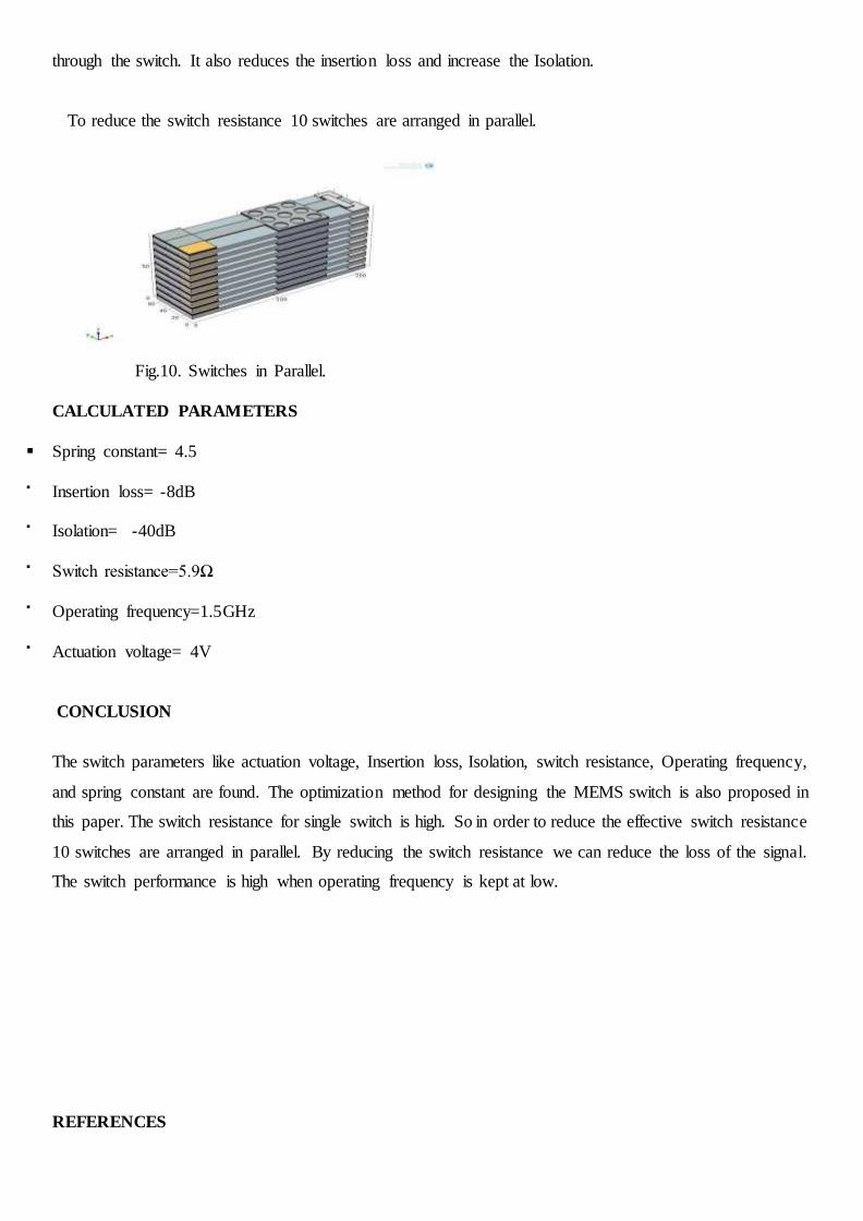
through the switch. It also reduces the insertion loss and increase the Isolation.
To reduce the switch resistance 10 switches are arranged in parallel.
Fig.10. Switches in Parallel.
CALCULATED PARAMETERS
Spring constant= 4.5
Insertion loss= -8dB
Isolation= -40dB
Switch resistance=5.9Ω
Operating frequency=1.5GHz
Actuation voltage= 4V
CONCLUSION
The switch parameters like actuation voltage, Insertion loss, Isolation, switch resistance, Operating frequency,
and spring constant are found. The optimization method for designing the MEMS switch is also proposed in
this paper. The switch resistance for single switch is high. So in order to reduce the effective switch resistance
10 switches are arranged in parallel. By reducing the switch resistance we can reduce the loss of the signal.
The switch performance is high when operating frequency is kept at low.
REFERENCES

[1]. G. M. Rebeiz, RF MEMS Theory, Design and Technology, 1st ed. Hoboken, NJ: Wiley, 2003.
[2]. Haslina Jaafar1, Member, IEEE, Fong Li Nan2,
NurulAmziahMd Yunus3 “Design and Simulation of High Performance RF MEMS Series Switch”, RSM2011 Proc.,
2011, Kota Kinabalu, Malaysia
[3] T. Kuenzig , G. Schrag J. Iannacci “study of an active thermal recovery mechanism for an electrostatically actuated RF-MEMS switch” Microelecromechanicalsystems 13th international conference on April 2012.
[4].RomainStefanini,Matthieuchatras,pierreBlondy,Gabriel
M.Rebeiz, “Miniature MEMS Switches for RF Applications”. Journal of Microelectromechanical systems, vol. 20, no. 6, December 20114.
[5]. Richard Chan, RobertLesnick, David Becher, and
Milton Feng “ low actuation voltage RF MEMS shunt switch with cold switching life time of seven billion cycles”
Journal of Microelectromechanical systems page number 713-719.
[6].Seong-Dae Lee, Byoung-Chul Jun, Sam-Dong Kim, Hyun-Chang Park, Jin-Koo Rhee, Koji Mizuno, ,
“An RF switch with low-actuation voltage and high reliability.
Journal of Microelectromechanical systems volume 15 page number 1605-1611.
[7].HojrSedaghat-Pisheh and Gabriel M.Rebeiz” Variable
Spring Constant, High Contact Force RF MEMS Switch”.
[8]. Y. Uno, K. Narise, T. Masuda, K. Inoue, Y. Adachi, K. Hosoya, T. Seki,and F. Satoe, “Development of SPDT-structured RF-MEMS switch,” inDenver, CO, Jun.
2009, pp.
541–544.
[9]. Jaehong Park, Eun Sub Shim, Wooyeol Choi, YoungminKim,YoungwooKwon,and Dong-il Cho, “A
Non-Contact-Type RF MEMS Switch N for 24-GHz Radar
Applications” Journal of Microelectromechanical systems, vol. 18, no. 1, February 2009.