VIBRATING RF MEMS FOR LOW POWER WIRELESS COMMUNICATIONSctnguyen/... · described with the intent to...
14
VIBRATING RF MEMS FOR LOW POWER WIRELESS COMMUNICATIONS Clark T.-C. Nguyen Center for Integrated Wireless Microsystems Department of Electrical Engineering and Computer Science University of Michigan Ann Arbor, Michigan 48109-2122 [email protected] ABSTRACT Micromechanical communication circuits fab- ricated via IC-compatible MEMS technologies and capable of low-loss filtering, mixing, switching, and frequency generation, are described with the intent to miniaturize wire- less transceivers. Possible transceiver front-end architectures are then presented that use these micromechanical circuits in large quantities to substantially reduce power consumption. Tech- nologies that integrate MEMS and transistor circuits into single-chip systems are then reviewed with an eye towards the possibility of single-chip communication transceivers. KEYWORDS resonator, communications, wireless, quality factor, RF MEMS, oscillator, bandpass filter, mixer, transceiver, receiver 1. INTRODUCTION Due to their need for high frequency selectivity and low noise frequency manipulation, porta- ble wireless communication transceivers con- tinue to rely on off-chip resonator technologies that interface with transistor electronics at the board-level. In particular, highly selective, low loss radio frequency (RF) and intermediate fre- quency (IF) bandpass filters generally require ceramic, SAW, or quartz acoustic resonator technologies with Q’s in excess of 1,000. In addition, LC resonator tanks with Q’s greater than 40 are required by voltage-controlled oscillators (VCO’s) to achieve sufficiently low phase noise. These off-chip resonator compo- nents then contribute to the substantial percent- age (often up to 80%) of portable transceiver area taken up by board-level, passive compo- nents. Recent advances in IC-compatible microelec- tromechanical system (MEMS) technologies that make possible micro-scale, mechanical cir- cuits capable of low-loss filtering, mixing, switching, and frequency generation, now sug- gest methods for boardless integration of wire- less transceiver components. In fact, given the existence already of technologies that merge micromechanics with transistor circuits onto single silicon chips [1]-[8], single-chip trans- ceivers may eventually be possible, perhaps using alternative architectures that maximize C. T.-C. Nguyen, “Vibrating RF MEMS for low power wireless communications (invited),” Pro- ceedings, 2000 Int. MEMS Workshop (iMEMS’01), Singapore, July 4-6, 2001, pp. 21-34.
Transcript of VIBRATING RF MEMS FOR LOW POWER WIRELESS COMMUNICATIONSctnguyen/... · described with the intent to...
VIBRATING RF MEMS FOR LOW POWER WIRELESS COMMUNICATIONS
Clark T.-C. Nguyen
Center for Integrated Wireless MicrosystemsDepartment of Electrical Engineering and Computer Science
University of MichiganAnn Arbor, Michigan 48109-2122
ABSTRACT
Micromechanical communication circuits fab-ricated via IC-compatible MEMS technologiesand capable of low-loss filtering, mixing,switching, and frequency generation, aredescribed with the intent to miniaturize wire-less transceivers. Possible transceiver front-endarchitectures are then presented that use thesemicromechanical circuits in large quantities tosubstantially reduce power consumption. Tech-nologies that integrate MEMS and transistorcircuits into single-chip systems are thenreviewed with an eye towards the possibility ofsingle-chip communication transceivers.
KEYWORDS
resonator, communications, wireless, qualityfactor, RF MEMS, oscillator, bandpass filter,mixer, transceiver, receiver
1. INTRODUCTION
Due to their need for high frequency selectivityand low noise frequency manipulation, porta-ble wireless communication transceivers con-tinue to rely on off-chip resonator technologies
that interface with transistor electronics at theboard-level. In particular, highly selective, lowloss radio frequency (RF) and intermediate fre-quency (IF) bandpass filters generally requireceramic, SAW, or quartz acoustic resonatortechnologies with Q’s in excess of 1,000. Inaddition, LC resonator tanks with Q’s greaterthan 40 are required by voltage-controlledoscillators (VCO’s) to achieve sufficiently lowphase noise. These off-chip resonator compo-nents then contribute to the substantial percent-age (often up to 80%) of portable transceiverarea taken up by board-level, passive compo-nents.
Recent advances in IC-compatible microelec-tromechanical system (MEMS) technologiesthat make possible micro-scale, mechanical cir-cuits capable of low-loss filtering, mixing,switching, and frequency generation, now sug-gest methods for boardless integration of wire-less transceiver components. In fact, given theexistence already of technologies that mergemicromechanics with transistor circuits ontosingle silicon chips [1]-[8], single-chip trans-ceivers may eventually be possible, perhapsusing alternative architectures that maximize
C. T.-C. Nguyen, “Vibrating RF MEMS for low power wireless communications (invited),” Pro-ceedings, 2000 Int. MEMS Workshop (iMEMS’01), Singapore, July 4-6, 2001, pp. 21-34.
the use of passive, high-Q, micromechanicalcircuits to reduce power consumption for por-table applications.
This paper presents an overview of the micro-mechanical circuits and associated technolo-gies expected to play key roles in reducing thesize and power consumption of future commu-nication transceivers.
2. MICROMECHANICAL CIRCUITS
Although mechanical circuits, such as quartzcrystal resonators and SAW filters, provideessential functions in the majority of trans-ceiver designs, their numbers are generallysuppressed due to their large size and finitecost. Unfortunately, when minimizing the useof high-Q components, designers often tradepower for selectivity (i.e., Q), and hence, sacri-fice transceiver performance.
By shrinking dimensions and introducing batchfabrication techniques, MEMS technology pro-vides a means for relaxing the present con-straints on the complexity of mechanicalcircuits, with implications not unlike those thatintegrated circuit technology had on transistorcircuit complexity [9], [10]. Before exploringthe implications, specific µmechanical circuitsare first reviewed.
2.1. Micromechanical Beam Element
To date, the majority of µmechanical circuits
most useful for communication functions havebeen realized using µmechanical flexural-mode beam elements, such as presented inFig. 1 with clamped-clamped boundary condi-tions. As shown, this device consists of a beamanchored (i.e., clamped) at both ends, with anelectrode underlying its central locations. Boththe beam and electrode are constructed of con-ductive materials, such as doped silicon, or ametal. Although several micromachining tech-nologies are available to realize such an ele-ment in a variety of different materials, surfacemicromachining [11] has so far been the pre-ferred method for µmechanical communicationcircuits, mainly due to its flexibility in provid-ing a variety of beam end conditions and elec-trode locations, and its ability to realize verycomplex geometries with multiple levels ofsuspension.
As shown in Fig. 1, the µmechanical beam ele-ment normally accepts two electrical inputs, veand vb, applied to the electrode and beam,respectively. In this configuration, the differ-ence voltage (ve − vb) is effectively appliedacross the electrode-to-resonator capacitor gap,generating a force between the stationary elec-trode and movable beam given by
(1)
where x is displacement (with direction indi-cated in Fig. 1), and (∂C/∂x) is the change in
Fig. 1: Perspective-view schematic of a clamped-clamped beam µmechanical resonator in a gen-eral bias and excitation configuration.
LrWr
d
Electrode
ve
io
h
Resonator Beam
vb
Wex
yz
Anchor
Fd∂E∂x------
12--- ve vb–( )2∂C
∂x-------= =
resonator-to-electrode capacitance per unit dis-placement (and is negative with the directionsindicated in Fig. 1). Depending upon the typeand frequency of the voltages applied to termi-nals e and b, this force can be tailored to spec-ify any one of a variety of signal processingfunctions available to the beam element. Asubset of the most useful of these is now sum-marized in the following sub-sections.
2.2. Micromechanical Reference Tanks
With Q’s in the thousands and ever-improvingthermal stabilities, single vibrating µmechani-cal beam elements are good candidates for useas frequency-setting tanks in reference oscilla-tor applications. When used as a tank or filtercircuit (as opposed to a mixer, to be discussedlater), a dc-bias voltage vb=VP is applied to theconductive beam, while an ac excitation signalve=Vicosωit is applied to the underlying elec-trode. In this configuration, a dominant forcecomponent is generated at ωi, which drives thebeam into mechanical resonance when ωi=ωo,creating a dc-biased (via VP) time-varyingcapacitance between the electrode and resona-tor, and sourcing an output current io=VP(∂C/∂x)(∂x/∂t), as shown in Fig. 1. When plottedversus the frequency of vi, io traces out a band-pass biquad characteristic with a Q~10,000 invacuum (c.f., Fig. 2 [15])—very suitable forreference oscillators.
The resonance frequency fo of a mechanicalresonator, such as the clamped-clampedbeam of Fig. 1, is governed by both materialproperties (e.g., Young’s modulus, density)and geometry (e.g., length, thickness). Forthe clamped-clamped beam of Fig. 1, theexpression for resonance frequency can bewritten as (ignoring stress and finite widtheffects) [15]
(2)
where kr and mr are the effective stiffness andmass of the beam at a given location; E and ρare the Young’s modulus and density of thestructural material, respectively; Lr is specifiedin Fig. 1; and heff is an effective thickness thatmodels the influence of surface topography onthe beam in actual implementations, [15], [16];and the function g models the action of a dc-bias dependent electrical stiffness that adds tomechanical stiffness of the beam, allowingsome voltage-control of its frequency. From(2), geometry clearly plays a major role in set-ting the resonance frequency, and in practice,attaining a specified frequency amounts toCAD layout of the proper dimensions.In gen-eral, the resonance frequency of a mechanicalresonator increases as its dimensions shrink(e.g., as the length of the beam in Fig. 1decreases)—thus, the utility of micro- or
Fig. 2: SEM of an 8.5 MHz clamped-clamped beam µmechanical resonator with a typicalmeasured spectrum [15].
µMechanicalAnchor
Electrodes
40.8µm
20 µm
Resonator
8µm
0.1µm
-25
-20
-15
-10
-5
0
8.48 8.49 8.50 8.51 8.52 8.53
Frequency [MHz]
Tra
nsm
issi
on
[d
B]
8.5 MHzQ = 8,000
Anchor
Clamped-ClampedBeam
MetallizedElectrode
Wr
Lr
hr
Polysilicon
Data:Lr=40.8µmWr=8µmh=2µm
d=1,300Åfo=8.5MHzQ=8,000
fo1
2π------
kr
mr------ 1.03
Eρ---
heff
Lr2
-------- 1 g VP( )–( )1 2/≅=
nano-scale mechanical resonators for VHF toUHF communication applications.
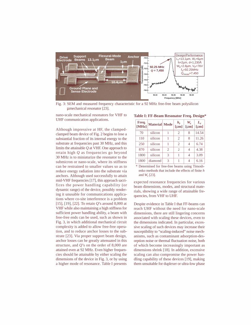
Although impressive at HF, the clamped-clamped beam device of Fig. 2 begins to lose asubstantial fraction of its internal energy to thesubstrate at frequencies past 30 MHz, and thislimits the attainable Q at VHF. One approach toretain high Q as frequencies go beyond30 MHz is to miniaturize the resonator to thesubmicron or nano-scale, where its stiffnesscan be restrained to smaller values so as toreduce energy radiation into the substrate viaanchors. Although used successfully to attainmid-VHF frequencies [17], this approach sacri-fices the power handling capability (ordynamic range) of the device, possibly render-ing it unusable for communications applica-tions where co-site interference is a problem[15], [19], [22]. To retain Q’s around 8,000 atVHF while also maintaining a high stiffness forsufficient power handling ability, a beam withfree-free ends can be used, such as shown inFig. 3, in which additional mechanical circuitcomplexity is added to allow free-free opera-tion, and to reduce anchor losses to the sub-strate [23]. Via proper support beam design,anchor losses can be greatly attenuated in thisstructure, and Q’s on the order of 8,000 areattained even at 92 MHz. Even higher frequen-cies should be attainable by either scaling thedimensions of the device in Fig. 3, or by usinga higher mode of resonance. Table I presents
expected resonance frequencies for variousbeam dimensions, modes, and structural mate-rials, showing a wide range of attainable fre-quencies, from VHF to UHF.
Despite evidence in Table I that FF-beams canreach UHF without the need for nano-scaledimensions, there are still lingering concernsassociated with scaling these devices, even tothe dimensions indicated. In particular, exces-sive scaling of such devices may increase theirsusceptibility to “scaling-induced” noise mech-anisms, such as contaminant adsorption-des-orption noise or thermal fluctuation noise, bothof which become increasingly important asdimensions shrink [18]. In addition, excessivescaling can also compromise the power han-dling capability of these devices [19], makingthem unsuitable for duplexer or ultra-low phase
74 µm
10.4µm
1µm13.1µm
Flexural-ModeSupport AnchorDrive Electrode BeamBeams
-76.5
-75.5
-74.5
-73.5
-72.5
-71.5
-70.5
92.22 92.24 92.26 92.28 92.30
Frequency [MHz]
Tra
nsm
issi
on
[d
B] 92.25 MHz
Q = 7,450
Ground Plane andSense Electrode
Fig. 3: SEM and measured frequency characteristic for a 92 MHz free-free beam polysiliconµmechanical resonator [23].
Design/Performance:Lr=13.1µm, Wr=6µmh=2µm, d=1,230Å
We=2.8µm, VP=76Vfo=92.25MHzQmeas=7,450
* Determined for free-free beams using Timosh-enko methods that include the effects of finite hand Wr [23].
Table I: FF-Beam Resonator Freq. Design*
Freq. [MHz]
Material Modehr
[µm]Wr
[µm]Lr
[µm]
70 silicon 1 2 8 14.54
110 silicon 1 2 8 11.26
250 silicon 1 2 4 6.74
870 silicon 2 2 4 4.38
1800 silicon 3 1 4 3.09
1800 diamond 3 1 4 6.16
noise oscillator applications.
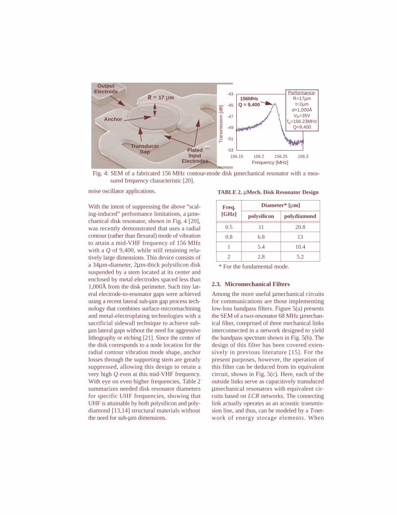
With the intent of suppressing the above “scal-ing-induced” performance limitations, a µme-chanical disk resonator, shown in Fig. 4 [20],was recently demonstrated that uses a radialcontour (rather than flexural) mode of vibrationto attain a mid-VHF frequency of 156 MHzwith a Q of 9,400, while still retaining rela-tively large dimensions. This device consists ofa 34µm-diameter, 2µm-thick polysilicon disksuspended by a stem located at its center andenclosed by metal electrodes spaced less than1,000Å from the disk perimeter. Such tiny lat-eral electrode-to-resonator gaps were achievedusing a recent lateral sub-µm gap process tech-nology that combines surface-micromachiningand metal-electroplating technologies with asacrificial sidewall technique to achieve sub-µm lateral gaps without the need for aggressivelithography or etching [21]. Since the center ofthe disk corresponds to a node location for theradial contour vibration mode shape, anchorlosses through the supporting stem are greatlysuppressed, allowing this design to retain avery high Q even at this mid-VHF frequency.With eye on even higher frequencies, Table 2summarizes needed disk resonator diametersfor specific UHF frequencies, showing thatUHF is attainable by both polysilicon and poly-diamond [13,14] structural materials withoutthe need for sub-µm dimensions.
2.3. Micromechanical Filters
Among the more useful µmechanical circuitsfor communications are those implementinglow-loss bandpass filters. Figure 5(a) presentsthe SEM of a two-resonator 68 MHz µmechan-ical filter, comprised of three mechanical linksinterconnected in a network designed to yieldthe bandpass spectrum shown in Fig. 5(b). Thedesign of this filter has been covered exten-sively in previous literature [15]. For thepresent purposes, however, the operation ofthis filter can be deduced from its equivalentcircuit, shown in Fig. 5(c). Here, each of theoutside links serve as capacitively transducedµmechanical resonators with equivalent cir-cuits based on LCR networks. The connectinglink actually operates as an acoustic transmis-sion line, and thus, can be modeled by a T-net-work of energy storage elements. When
R = 17 µm
Plated
Electrodes
OutputElectrode
Anchor
TransducerGap
Input-53
-51
-49
-47
-45
-43
156.15 156.2 156.25 156.3
Frequency [MHz]
Tran
smis
sion
[dB
]
156MHzQ = 9,400
Fig. 4: SEM of a fabricated 156 MHz contour-mode disk µmechanical resonator with a mea-sured frequency characteristic [20].
Performance:R=17µmt=2µm
d=1,000ÅVP=35V
fo=156.23MHzQ=9,400
* For the fundamental mode.
TABLE 2. µMech. Disk Resonator Design
Freq.[GHz]
Diameter* [µm]
polysilicon polydiamond
0.5 11 20.8
0.8 6.8 13
1 5.4 10.4
2 2.8 5.2
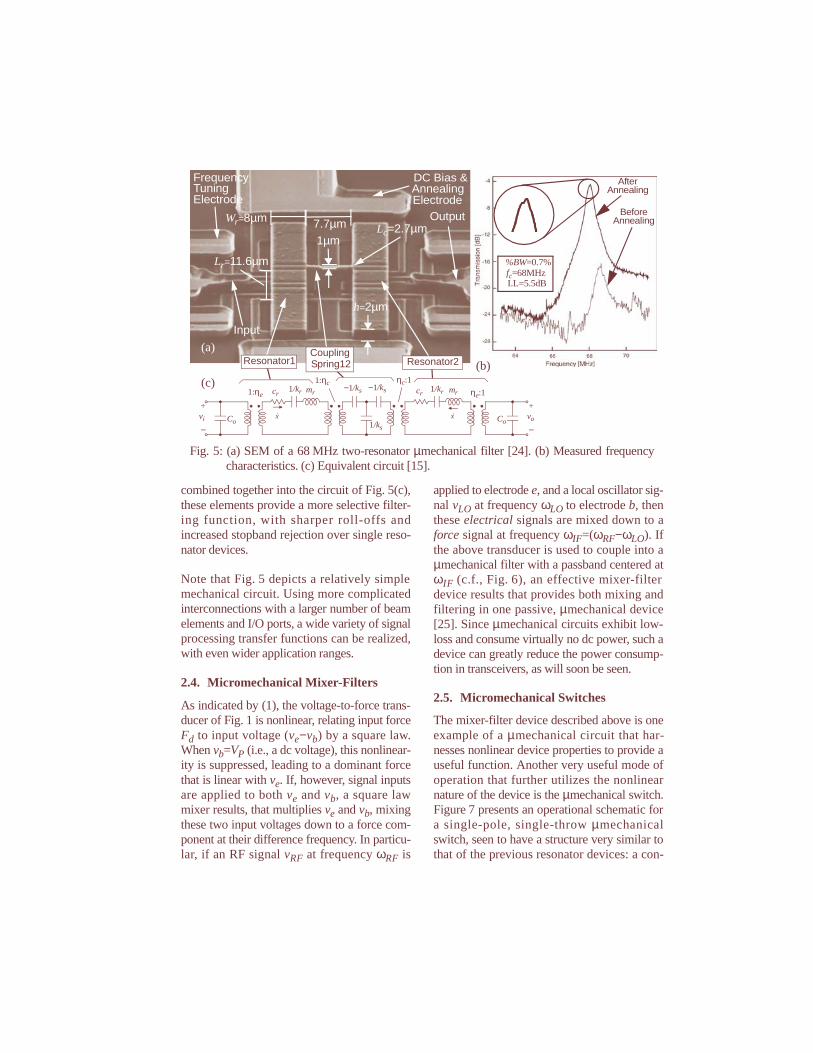
combined together into the circuit of Fig. 5(c),these elements provide a more selective filter-ing function, with sharper roll-offs andincreased stopband rejection over single reso-nator devices.
Note that Fig. 5 depicts a relatively simplemechanical circuit. Using more complicatedinterconnections with a larger number of beamelements and I/O ports, a wide variety of signalprocessing transfer functions can be realized,with even wider application ranges.
2.4. Micromechanical Mixer-Filters
As indicated by (1), the voltage-to-force trans-ducer of Fig. 1 is nonlinear, relating input forceFd to input voltage (ve−vb) by a square law.When vb=VP (i.e., a dc voltage), this nonlinear-ity is suppressed, leading to a dominant forcethat is linear with ve. If, however, signal inputsare applied to both ve and vb, a square lawmixer results, that multiplies ve and vb, mixingthese two input voltages down to a force com-ponent at their difference frequency. In particu-lar, if an RF signal vRF at frequency ωRF is
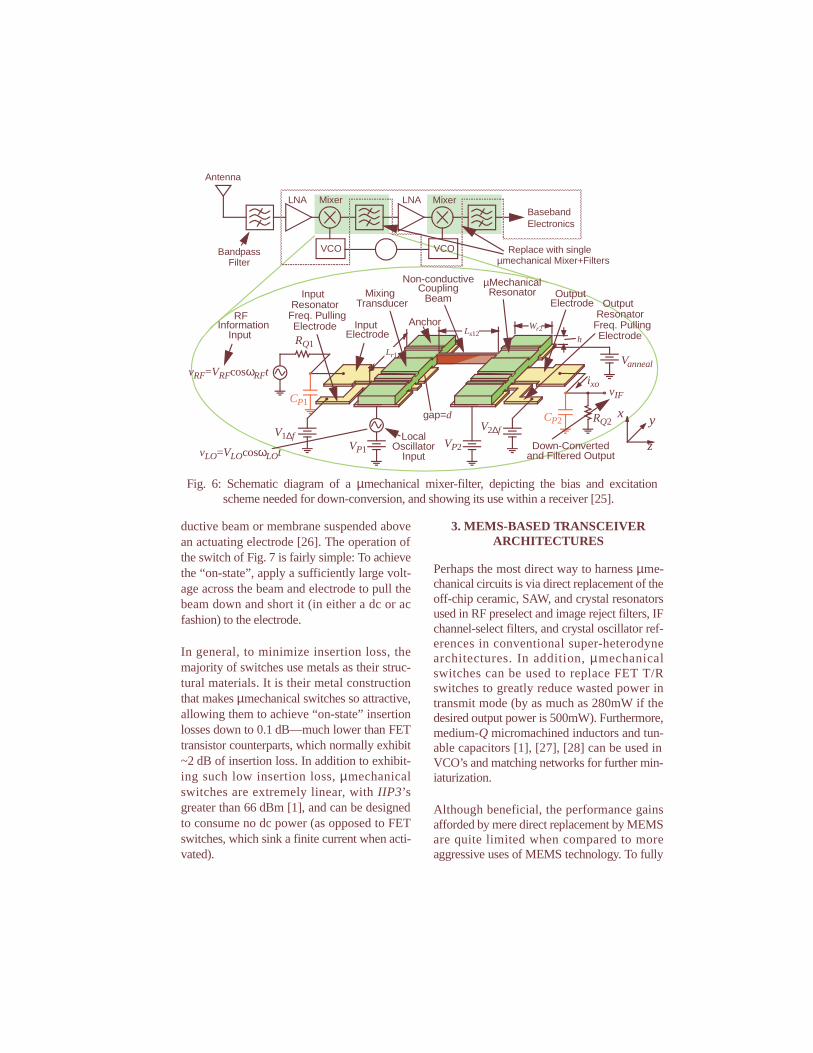
applied to electrode e, and a local oscillator sig-nal vLO at frequency ωLO to electrode b, thenthese electrical signals are mixed down to aforce signal at frequency ωIF=(ωRF−ωLO). Ifthe above transducer is used to couple into aµmechanical filter with a passband centered atωIF (c.f., Fig. 6), an effective mixer-filterdevice results that provides both mixing andfiltering in one passive, µmechanical device[25]. Since µmechanical circuits exhibit low-loss and consume virtually no dc power, such adevice can greatly reduce the power consump-tion in transceivers, as will soon be seen.
2.5. Micromechanical Switches
The mixer-filter device described above is oneexample of a µmechanical circuit that har-nesses nonlinear device properties to provide auseful function. Another very useful mode ofoperation that further utilizes the nonlinearnature of the device is the µmechanical switch.Figure 7 presents an operational schematic fora single-pole, single-throw µmechanicalswitch, seen to have a structure very similar tothat of the previous resonator devices: a con-
Fig. 5: (a) SEM of a 68 MHz two-resonator µmechanical filter [24]. (b) Measured frequencycharacteristics. (c) Equivalent circuit [15].
DC Bias & Frequency Tuning Electrode
Resonator
DC Bias &AnnealingElectrode
Frequency Tuning Electrode
Input
Output
1µm
h=2µm
Lr=11.6µm
7.7µm Lc=2.7µmWr=8µm
cr mr
1/ks
1/kr−1/ks−1/ks
1:ηc ηc:1
Covi
+
−
cr mr1/kr
Covo
+
−
1:ηe ηe:1
x·x·
Resonator1 Spring12Coupling
Resonator2
After
Before
%BW=0.7%fc=68MHzI.L=5.5dB
Annealing
Annealing
(b)(c)
(a)
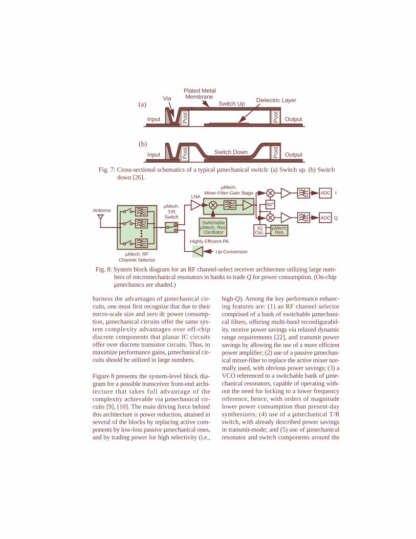
ductive beam or membrane suspended abovean actuating electrode [26]. The operation ofthe switch of Fig. 7 is fairly simple: To achievethe “on-state”, apply a sufficiently large volt-age across the beam and electrode to pull thebeam down and short it (in either a dc or acfashion) to the electrode.
In general, to minimize insertion loss, themajority of switches use metals as their struc-tural materials. It is their metal constructionthat makes µmechanical switches so attractive,allowing them to achieve “on-state” insertionlosses down to 0.1 dB—much lower than FETtransistor counterparts, which normally exhibit~2 dB of insertion loss. In addition to exhibit-ing such low insertion loss, µmechanicalswitches are extremely linear, with IIP3’sgreater than 66 dBm [1], and can be designedto consume no dc power (as opposed to FETswitches, which sink a finite current when acti-vated).
3. MEMS-BASED TRANSCEIVER ARCHITECTURES
Perhaps the most direct way to harness µme-chanical circuits is via direct replacement of theoff-chip ceramic, SAW, and crystal resonatorsused in RF preselect and image reject filters, IFchannel-select filters, and crystal oscillator ref-erences in conventional super-heterodynearchitectures. In addition, µmechanicalswitches can be used to replace FET T/Rswitches to greatly reduce wasted power intransmit mode (by as much as 280mW if thedesired output power is 500mW). Furthermore,medium-Q micromachined inductors and tun-able capacitors [1], [27], [28] can be used inVCO’s and matching networks for further min-iaturization.
Although beneficial, the performance gainsafforded by mere direct replacement by MEMSare quite limited when compared to moreaggressive uses of MEMS technology. To fully
Fig. 6: Schematic diagram of a µmechanical mixer-filter, depicting the bias and excitationscheme needed for down-conversion, and showing its use within a receiver [25].
BasebandElectronics
LNA LNAMixer
VCOVCO
Mixer
Antenna
Replace with singleµmechanical Mixer+Filters
BandpassFilter
V1∆f
Anchor
OutputElectrode
InputElectrode
Input
Freq. PullingElectrode
Resonator Output
Freq. PullingElectrode
Resonator
RQ2CP2
RQ1
CP1
V2∆f
MixingTransducer
µMechanicalResonator
vIF
vRF=VRFcosωRFt
InformationInput
vLO=VLOcosωLOt
RF
Down-Convertedand Filtered Output
Vanneal
Wr2
Lr1
Ls12h
BeamCoupling
Non-conductive
LocalOscillator
Input
x y
z
gap=d
ixo
VP1VP2
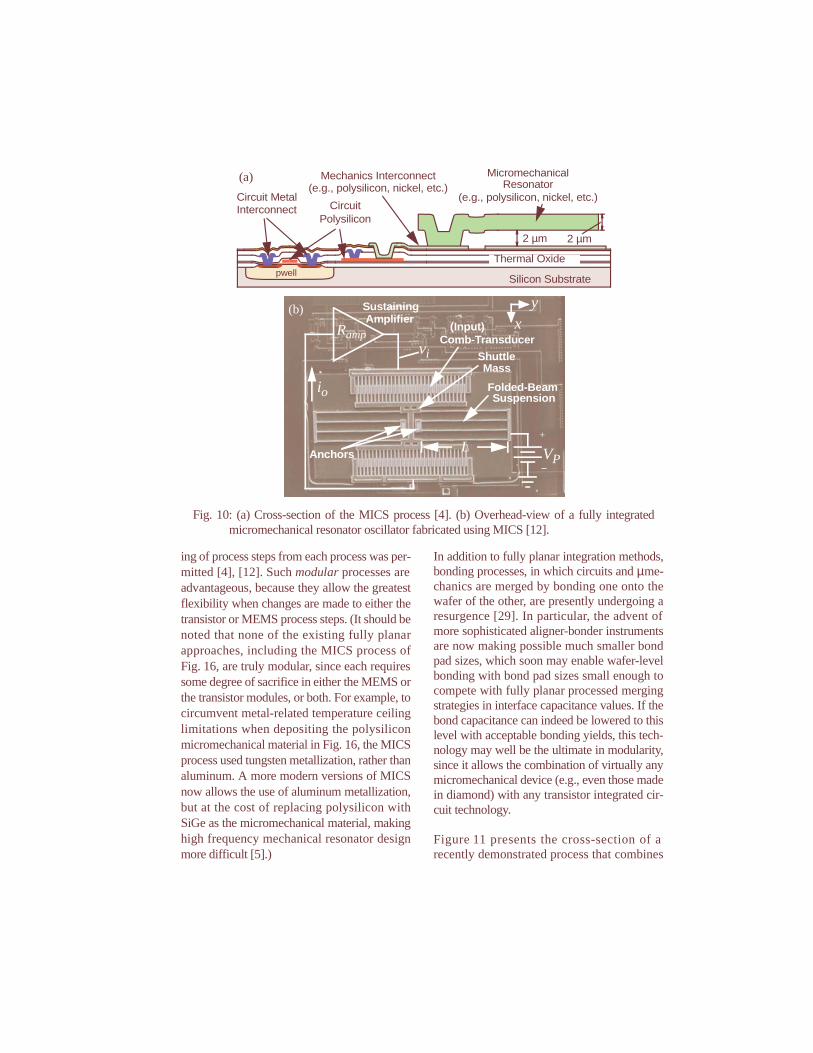
harness the advantages of µmechanical cir-cuits, one must first recognize that due to theirmicro-scale size and zero dc power consump-tion, µmechanical circuits offer the same sys-tem complexity advantages over off-chipdiscrete components that planar IC circuitsoffer over discrete transistor circuits. Thus, tomaximize performance gains, µmechanical cir-cuits should be utilized in large numbers.
Figure 8 presents the system-level block dia-gram for a possible transceiver front-end archi-tecture that takes full advantage of thecomplexity achievable via µmechanical cir-cuits [9], [10]. The main driving force behindthis architecture is power reduction, attained inseveral of the blocks by replacing active com-ponents by low-loss passive µmechanical ones,and by trading power for high selectivity (i.e.,
high-Q). Among the key performance enhanc-ing features are: (1) an RF channel selectorcomprised of a bank of switchable µmechani-cal filters, offering multi-band reconfigurabil-ity, receive power savings via relaxed dynamicrange requirements [22], and transmit powersavings by allowing the use of a more efficientpower amplifier; (2) use of a passive µmechan-ical mixer-filter to replace the active mixer nor-mally used, with obvious power savings; (3) aVCO referenced to a switchable bank of µme-chanical resonators, capable of operating with-out the need for locking to a lower frequencyreference, hence, with orders of magnitudelower power consumption than present-daysynthesizers; (4) use of a µmechanical T/Rswitch, with already described power savingsin transmit-mode; and (5) use of µmechanicalresonator and switch components around the
Fig. 7: Cross-sectional schematics of a typical µmechanical switch: (a) Switch up. (b) Switchdown [26].
Switch Down OutputInput Pos
t
Pos
t
Switch Up
OutputInput Pos
t
Pos
t
Dielectric LayerViaPlated MetalMembrane
(a)
(b)
Fig. 8: System block diagram for an RF channel-select receiver architecture utilizing large num-bers of micromechanical resonators in banks to trade Q for power consumption. (On-chipµmechanics are shaded.)
I
Q
LNA
90o
ADC
ADC
IQOsc.
µMech.Res.
SwitchableµMech. Res.
Oscillator
µMech.Mixer-Filter-Gain Stage
µMech. RFChannel Selector
AntennaSwitch
T/RµMech.
Up-Conversion
Highly Efficient PA

power amplifier to enhance its efficiency.
Although already quite aggressive, the archi-tecture of Fig. 8 may still not represent the bestpower savings afforded by MEMS. In fact,even more power savings than in Fig. 8 arepossible if the high-Q µmechanical circuits inthe signal path can post such low losses that theRF LNA (normally required to boost thereceived signal against losses and noise fromsubsequent stages) may in fact no longer beneeded. Rather, the RF LNA can be removed,and the needed gain to baseband providedinstead by an IF LNA that consumes much lesspower since it operates at the much lower IFfrequency. Without the RF LNA or transistormixer, the receiver front-end architecturereduces to an all-MEMS topology, such asshown in Fig. 9. Here, since the absence of RFtransistor circuits removes dynamic range con-cerns, the channel-selecting filter bank of Fig. 8has been converted to a mixer-filter bank andmoved down to the IF frequency, where itmight be easier to implement, and where itallows the use of a single-frequency RF localoscillator (LO) to down-convert from RF toIF. Since the RF LO is now a single frequencyoscillator, power hungry phase-locking andpre-scaling electronics are not needed, allow-ing similar power advantages as for the VCOin the architecture of Fig. 8. In fact, the archi-tecture of Fig. 9 attains all the power advan-tages of that of Fig. 8, plus additional power
savings due to the lack of an LNA. It, how-ever, does so at the cost of a slightly higheroverall noise figure and decreased robustnessagainst hostile (i.e., jamming) interferers.
4. CIRCUITS/MEMS MERGING TECHNOLOGIES
Although a two-chip solution that combines aMEMS chip with a transistor chip can certainlybe used to interface µmechanical circuits withtransistor circuits, such an approach becomesless practical as the number of µmechanicalcomponents increases. For instance, practicalimplementations of the switchable filter bankin Fig. 8 require multiplexing support electron-ics that must interconnect with each µmechani-cal device. If implemented using a two-chipapproach, the number of chip-to-chip bondsrequired could become quite cumbersome,making a single-chip solution desirable.
In the pursuit of single-chip systems, severaltechnologies that merge micromachining pro-cesses with those for integrated circuits havebeen developed and implemented over the pastseveral years [2]-[8]. Figure 10 presents thecross-section and overhead SEM of one suchtechnology that combined CMOS transistorcircuits and polysilicon surface micromachinedstructures in a fully planar, modular fashion,where transistor and MEMS fabrication stepswere separated into modules, and no intermix-
IFAmp
90o
ADC
ADC
IQOsc.
µMech.Res.
µMech.Image-Reject
RF Filter
Antenna1Antenna2
µMech.Switch
SingleµMech. Res.
Oscillator
I
Q
µMech. Mixer-FilterIF Channel-Selector
Fig. 9: System block diagram for an all-MEMS receiver front-end, employing an RF image-reject filter, a fixed µmechanical resonator local oscillator, and a switchable array of IFµmechanical mixer-filters.
ing of process steps from each process was per-mitted [4], [12]. Such modular processes areadvantageous, because they allow the greatestflexibility when changes are made to either thetransistor or MEMS process steps. (It should benoted that none of the existing fully planarapproaches, including the MICS process ofFig. 16, are truly modular, since each requiressome degree of sacrifice in either the MEMS orthe transistor modules, or both. For example, tocircumvent metal-related temperature ceilinglimitations when depositing the polysiliconmicromechanical material in Fig. 16, the MICSprocess used tungsten metallization, rather thanaluminum. A more modern versions of MICSnow allows the use of aluminum metallization,but at the cost of replacing polysilicon withSiGe as the micromechanical material, makinghigh frequency mechanical resonator designmore difficult [5].)
In addition to fully planar integration methods,bonding processes, in which circuits and µme-chanics are merged by bonding one onto thewafer of the other, are presently undergoing aresurgence [29]. In particular, the advent ofmore sophisticated aligner-bonder instrumentsare now making possible much smaller bondpad sizes, which soon may enable wafer-levelbonding with bond pad sizes small enough tocompete with fully planar processed mergingstrategies in interface capacitance values. If thebond capacitance can indeed be lowered to thislevel with acceptable bonding yields, this tech-nology may well be the ultimate in modularity,since it allows the combination of virtually anymicromechanical device (e.g., even those madein diamond) with any transistor integrated cir-cuit technology.
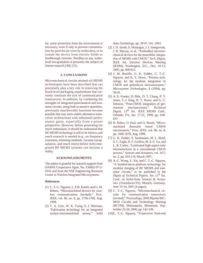
Figure 11 presents the cross-section of arecently demonstrated process that combines
Fig. 10: (a) Cross-section of the MICS process [4]. (b) Overhead-view of a fully integratedmicromechanical resonator oscillator fabricated using MICS [12].
Sustaining
Ramp
VP
+
−
vi
io
Anchors
Folded-BeamSuspension
Comb-Transducer
ShuttleMass
Amplifier xy
(Input)
L
Mechanics Interconnect
pwellSilicon Substrate
(e.g., polysilicon, nickel, etc.)
2 µm
MicromechanicalResonator
(e.g., polysilicon, nickel, etc.)Circuit MetalInterconnect Circuit
Polysilicon
2 µm
Thermal Oxide
(a)
(b)
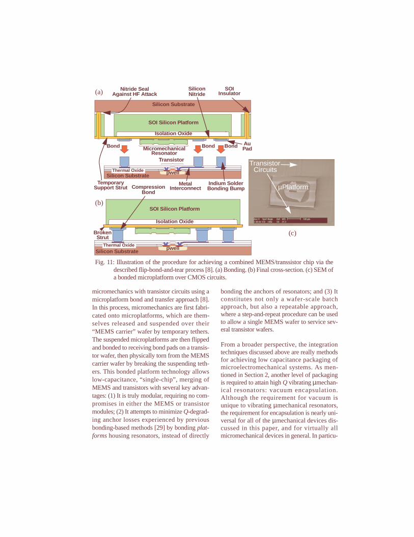
micromechanics with transistor circuits using amicroplatform bond and transfer approach [8].In this process, micromechanics are first fabri-cated onto microplatforms, which are them-selves released and suspended over their“MEMS carrier” wafer by temporary tethers.The suspended microplatforms are then flippedand bonded to receiving bond pads on a transis-tor wafer, then physically torn from the MEMScarrier wafer by breaking the suspending teth-ers. This bonded platform technology allowslow-capacitance, “single-chip”, merging ofMEMS and transistors with several key advan-tages: (1) It is truly modular, requiring no com-promises in either the MEMS or transistormodules; (2) It attempts to minimize Q-degrad-ing anchor losses experienced by previousbonding-based methods [29] by bonding plat-forms housing resonators, instead of directly
bonding the anchors of resonators; and (3) Itconstitutes not only a wafer-scale batchapproach, but also a repeatable approach,where a step-and-repeat procedure can be usedto allow a single MEMS wafer to service sev-eral transistor wafers.
From a broader perspective, the integrationtechniques discussed above are really methodsfor achieving low capacitance packaging ofmicroelectromechanical systems. As men-tioned in Section 2, another level of packagingis required to attain high Q vibrating µmechan-ical resonators: vacuum encapsulation.Although the requirement for vacuum isunique to vibrating µmechanical resonators,the requirement for encapsulation is nearly uni-versal for all of the µmechanical devices dis-cussed in this paper, and for virtually allmicromechanical devices in general. In particu-
pwell
SOI Silicon Platform
Isolation Oxide
Silicon Substrate
Nitride Seal SOIInsulator
BondBond
Silicon
Indium Solder
Against HF Attack
pwellSilicon Substrate
CompressionBond
SOI Silicon Platform
Isolation Oxide
Nitride
Thermal Oxide
MicromechanicalResonator
Transistor
MetalInterconnect
TemporarySupport Strut Bonding Bump
Silicon Substrate
Bond
Thermal Oxide
BrokenStrut
(a)
(b)
AuPad
Fig. 11: Illustration of the procedure for achieving a combined MEMS/transsistor chip via thedescribed flip-bond-and-tear process [8]. (a) Bonding. (b) Final cross-section. (c) SEM ofa bonded microplatform over CMOS circuits.
µPlatform
TransistorCircuits
(c)
lar, some protection from the environment isnecessary, even if only to prevent contamina-tion by particles (or even by molecules), or toisolate the device from electric fields orfeedthrough currents. Needless to say, wafer-level encapsulation is presently the subject ofintense research [30], [31].
5. CONCLUSIONS
Micromechanical circuits attained via MEMStechnologies have been described that canpotentially play a key role in removing theboard-level packaging requirements that cur-rently constrain the size of communicationtransceivers. In addition, by combining thestrengths of integrated µmechanical and tran-sistor circuits, using both in massive quantities,previously unachievable functions becomepossible that may soon enable alternative trans-ceiver architectures with substantial perfor-mance gains, especially from a powerperspective. However, before generating toomuch enthusiasm, it should be understood thatRF MEMS technology is still in its infancy, andmuch research is needed (e.g., on frequencyextension, trimming methods, vacuum encap-sulation, and much more) before fully-inte-grated RF MEMS systems can become areality.
ACKNOWLEDGMENTS
The author is grateful for research support fromDARPA Cooperative Agmt. No. F30602-97-2-0101 and from the NSF Engineering ResearchCenter in Wireless Integrated Microsystems.
References
[1] C. T.-C. Nguyen, L. P.B. Katehi, and G. M.Rebeiz, “Micromachined devices for wire-less communications (invited),” Proc.IEEE, vol. 86, no. 8, pp. 1756-1768, Aug.1998.
[2] T. A. Core, W. K. Tsang, S. J. Sherman,“Fabrication technology for an integratedsurface-micromachined sensor,” Solid
State Technology, pp. 39-47, Oct. 1993.[3] J. H. Smith, S. Montague, J. J. Sniegowski,
J. R. Murray, et al., “Embedded microme-chanical devices for the monolithic integra-tion of MEMS with CMOS,” Tech. Digest,IEEE Int. Electron Devices Meeting(IEDM), Washington, D.C., Dec. 10-13,1995, pp. 609-612.
[4] J. M. Bustillo, G. K. Fedder, C. T.-C.Nguyen, and R. T. Howe, “Process tech-nology for the modular integration ofCMOS and polysilicon microstructures,”Microsystem Technologies, 1 (1994), pp.30-41.
[5] A. E. Franke, D. Bilic, D. T. Chang, P. T.Jones, T.-J. King, R. T. Howe, and G. C.Johnson, “Post-CMOS integration of ger-manium microstructures,” TechnicalDigest, 12th Int. IEEE MEMS Conf.,Orlando, FA, Jan. 17-21, 1999, pp. 630-637.
[6] H. Baltes, O. Paul, and O. Brand, “Micro-machined thermally based CMOSmicrosensors,” Proc. IEEE, vol. 86, no. 8,pp. 1660-1678, Aug. 1998.
[7] G. K. Fedder, S. Santhanam, M. L. Reed,S. C. Eagle, D. F. Guillou, M. S.-C. Lu, andL. R. Carley, “Laminated high-aspect-ratiomicrostructures in a conventional CMOSprocess,” Sensors and Actuators, vol. A57,no. 2, pp. 103-110, March 1997.
[8] A.-C. Wong, Y. Xie, and C. T.-C. Nguyen,“A bonded-micro-platform technology formodular merging of RF MEMS and tran-sistor circuits,” to be published in theDigest of Technical Papers, the 11th Int.Conf. on Solid-State Sensors & Actua-tors (Transducers’01), Munich, Germany,June 10-14, 2001 (4 pages).
[9] C. T.-C. Nguyen, “Micromechanical cir-cuits for communication transceivers(invited),” Proceedings, 2000 Bipolar/BiC-MOS Circuits and Technology Meeting(BCTM), Minneapolis, Minnesota, Sep-tember 25-26, 2000, pp. 142-149.
[10]C. T.-C. Nguyen, “Transceiver front-end
architectures using vibrating micromechan-ical signal processors,” to be published inLow Power Communications Electronics,edited by G. I. Haddad, T. Itoh, and J. Har-vey (35 pages).
[11]J. M. Bustillo, R. T. Howe, and R. S.Muller, “Surface micromachining formicroelectromechanical systems(invited),” Proc. IEEE, vol. 86, no. 8, pp.1552-1574, Aug. 1998.
[12]C. T.-C. Nguyen and R. T. Howe, “Anintegrated CMOS micromechanical reso-nator high-Q oscillator,” IEEE J. Solid-State Circuits, vol. 34, no. 4, pp. 440-445,April 1999.
[13]D. Aslam, V. Pappageorgiou, et al., “IC-compatible technology of polydiamondMEMS,” Proceedings, 6th Annual Symp.on Vehicular Appl. of Displays andMicrosensors, Ypsilanti, Michigan, Sept.22-23, 1999.
[14]M. Aslam and D. Schulz, “Technology ofDiamond Microelectromechanical Sys-tems,” Technical Digest: 8th Int. Conf.Solid-State Sensor & Actuators, Stockholm(Sweden), Vol. 2, 222-224 (1995).
[15]F. D. Bannon III, J. R. Clark, and C. T.-C.Nguyen, “High frequency micromechani-cal filters,” IEEE J. Solid-State Circuits,vol. 35, no. 4, pp. 512-526, April 2000.
[16]Q. Meng, M. Mehregany, and R. L.Mullen, “Theoretical modelling of micro-fabricated beams with elastically restrainedsupports,” J. Microelectromech. Syst., vol.2, no. 3, pp. 128-137, Sept. 1993.
[17]A. N. Cleland and M. L. Roukes, “Fabrica-tion of high frequency nanometer scalemechanical resonators from bulk Si crys-tals,” Appl. Phys. Lett., 69 (18), pp. 2653-2655, Oct. 28, 1996.
[18]J. R. Vig and Y. Kim, “Noise in microelec-tromechanical system resonators,” IEEETrans. Utrason. Ferroelec. Freq. Contr.,vol. 46, no. 6, pp. 1558-1565, Nov. 1999.
[19]R. Navid, J. R. Clark, M. Demirci, and C.T.-C. Nguyen, “Third-order intermodula-
tion distortion in capacitively-driven CC-beam micromechanical resonators,” Tech-nical Digest, 14th Int. IEEE Micro ElectroMechanical Systems Conference, Inter-laken, Switzerland, Jan. 21-25, 2001, pp.228-231.
[20]J. R. Clark, W.-T. Hsu, and C. T.-C.Nguyen, “High-Q VHF micromechanicalcontour-mode disk resonators,” TechnicalDigest, IEEE Int. Electron Devices Meet-ing, San Francisco, California, Dec. 11-13,2000, pp. 399-402.
[21]W.-T. Hsu, J. R. Clark, and C. T.-C.Nguyen, “A sub-micron capacitive gapprocess for multiple-metal-electrode lat-eral micromechanical resonators,” Techni-cal Digest, 14th Int. IEEE Micro ElectroMechanical Systems Conference, Inter-laken, Switzerland, Jan. 21-25, 2001, pp.349-352.
[22]C. T.-C. Nguyen, “Frequency-selectiveMEMS for miniaturized low-power com-munication devices,” IEEE Trans. Micro-wave Theory Tech., vol. 47, no. 8, pp.1486-1503, Aug. 1999.
[23]K. Wang, A.-C. Wong, and C. T.-C.Nguyen, “VHF free-free beam high-Qmicromechanical resonators,” IEEE/ASMEJ. Microelectromech. Syst., vol. 9, no. 3,pp. 347-360, Sept. 2000.
[24]A.-C. Wong, J. R. Clark, and C. T.-C.Nguyen, “Anneal-activated, tunable,68MHz micromechanical filters” Digest ofTechnical Papers, 10th Int. Conf. onSolid-State Sensors and Actuators, Sendai,Japan, June 7-10, 1999, pp. 1390-1393.
[25]A.-C. Wong, H. Ding, and C. T.-C.Nguyen, “Micromechanical mixer+filters,”Tech. Digest, IEEE Int. Electron DevicesMeeting (IEDM), San Francisco, Califor-nia, Dec. 6-9, 1998, pp. 471-474.
[26]C. Goldsmith, J. Randall, S. Eshelman, T.H. Lin, D. Denniston, S. Chen and B. Nor-vell, “Characteristics of micromachinedswitches at microwave frequencies,” IEEEMTT-S Digest, pp. 1141-1144, June, 1996.
[27]D. J. Young and B. E. Boser, “A microma-chined variable capacitor for monolithiclow-noise VCOs,” Technical Digest, 1996Solid-State Sensor and Actuator Work-shop, Hilton Head Island, South Carolina,June 3-6, 1996, pp. 86-89.
[28]J.-B. Yoon, C.-H. Han, E. Yoon, and C.-K.Kim, “Monolithic high-Q overhand induc-tors fabricated on silicon and glass sub-strates,” Technical Digest, IEEE IEDM,Washington, D. C., Dec. 5-8, 1999, pp.753-756.
[29]A. Singh, D. A. Horsley, M. B. Cohn, A. P.Pisano, and R. T. Howe, “Batch transfer ofmicrostructures using flip-chip solderbonding,” J. Microelectromech. Syst., vol.8, no. 1, pp. 27-33, March 1999.
[30]K. S. Lebouitz, A. Mazaheri, R. T. Howe,and A. P. Pisano, “Vacuum encapsulationof resonant devices using permeable poly-silicon,” Technical Digest, 12th Int. IEEEMEMS Conf., Orlando, Florida, Jan. 17-21, 1999, pp. 470-475.
[31]Y.-T. Cheng, W.-T. Hsu, L. Lin, C. T.-C.Nguyen, and K. Najafi, “Vacuum packag-ing using localized aluminum/silicon-to-glass bonding,” Technical Digest, 14th Int.IEEE Micro Electro Mechanical SystemsConference, Interlaken, Switzerland, Jan.21-25, 2001, pp. 18-21.