Embedded Wafer-Level-Packages - Market Research … · · 2011-08-06Embedded Wafer-Level-Packages...
19
© 2010 Copyrights © Yole Développement SARL. All rights reserved. Embedded Wafer-Level-Packages Fan-Out WLP / Chip Embedding in Substrate Be ready for the next generation of IC packaging & substrate assembly waves! Infineon Nokia FCI NXP STATs ChipPAC AT&S
-
Upload
dinhkhuong -
Category
Documents
-
view
224 -
download
2
Transcript of Embedded Wafer-Level-Packages - Market Research … · · 2011-08-06Embedded Wafer-Level-Packages...

© 2010
Copyrights © Yole Développement SARL. All rights reserved.
Embedded Wafer-Level-PackagesFan-Out WLP / Chip Embedding in Substrate
Be ready for the next generation of
IC packaging & substrate assembly waves!
Infineon
Nokia FCI
NXP STATs ChipPAC
AT&S

© 2010 • 2Copyrights © Yole Développement SARL. All rights reserved.
– Technology flavors for embedded package ... 51
• Chip first versus chip last?
• Single die embedding versus SiP module?
SiP multi-die integration
Discrete passive integration
Specific features integration (silicon interposers,
holes, fluidic, hermetic cavities, etc…)
• Challenges related to yield & supply chain
– Equt & Material Tool-Box for Embedded die … 78
– Cost structure for Embedded package
manufacturing …………………………………..... 95
• Comparison with competitive package alternative
that Embedded die technology is looking for direct
replacement (QFN, BGA, WLCSP, SOT, PoP…)
• Cost structure target of Embedded die for different
application case (RFID, IPD, Power MOSFET / IGBT,
DC/DC converters, PMU, Wireless Connectivity ICs,
Digital Baseband, Memories, etc …)
– Conclusion on “sweets spots” for the
introduction of Embedded die technology in the
short / medium / long term ……………………. 102
• Global Roadmap for Embedded die
Table of Contents (1/2)
• Scope of the Report & Definitions …...……. 3
– Objectives of the report ………….……... 4
• Executive Summary ………………………..… 9
1) Embedded Packaging of active dies and
passive components ………………….……. 10
– Motivations and Drivers ………………... 18
– Applications & End-markets: Status of
commercialization …………………..…... 24
• Cell-phone & Consumer applications
• Automotive applications
• Medical applications
– 2009-2015 market forecasts for Embedded
packages ………………………………….... 32
• In Package shipments (Munits)
• In Packaging revenues ($M)
– Supply chain emerging for embedded dies
………………………………….…………….. 44
• Players and positioning in the electronic value
chain
• Who is the most aggressive in the
commercialization?
• Who is doing what: partnership identified
© 2010 • 3Copyrights © Yole Développement SARL. All rights reserved.
– Cost structure for FO-WLP manufacturing
• Competitive package alternative that FOWLP
technology is looking for direct replacement
(FC-CSP, FC-BGA, WB-BGA, PoP, etc…)
• Cost structure for FOWLP by application (RF
connectivity, Transceiver, PMU, wireless
baseband SOC chip, etc…)
– Conclusion on “sweets spots” for
introduction of FOWLP technology in short
/ medium / long term
– Global Roadmap for Fan-Out WLP
• Conclusion & Perspectives ….……… 136
– Application space for each generation of
FO-WLP & Embedded die technology
– Impact of 3D TSV and silicon interposer
technology concepts
– Global 3D Packaging development
roadmaps mixing interposer, FOWLP and
Embedded die technologies
• Appendix ……....…………….…….…… 152– Yole Developpement company
presentation & services ..................... 183
Table of Contents (2/2)
2) Fan-Out WLP technology development … 120
– Motivations and market drivers ………….... 44
• Thermal performance of FOWLP package
compared to FC-BGA package solution
– Applications & status of commercialization
– 2009-2015 market forecasts for FOWLP type of
packages …………………………………….... 32
• In Package shipments (Munits)
• In Packaging revenues ($M)
– Supply chain emerging for FOWLP ……….. 44
• Players and positioning in the electronic value
chain
• Who is the most aggressive in the
commercialization?
• Who is doing what: partnership identified
– FOWLP technologies and challenges
• Who owns the IP in this space?
• 1st generation versus 2nd generation FOWLP
– TMV “Through Mold Via” fabrication
• “Panel size” future manufacturing for FOWLP
• Passive integration with FO-WLP technologies
– Equipment & Materials for FO-WLP
• Challenges in new material‟s selection and
missing equipments
© 2010 • 4Copyrights © Yole Développement SARL. All rights reserved.
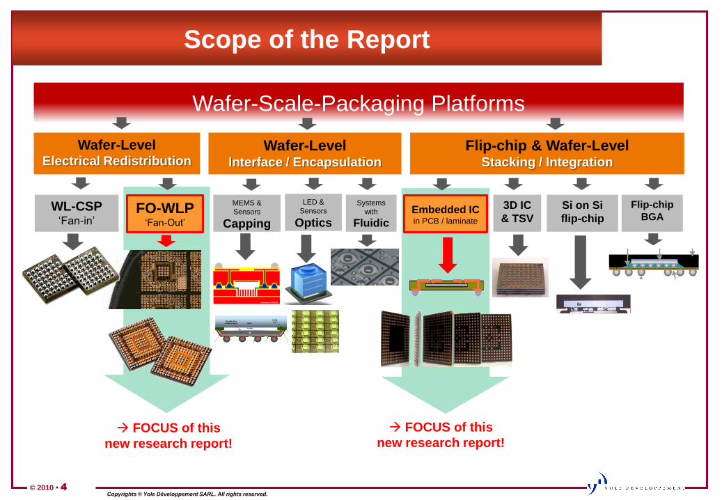
Scope of the Report
Wafer-Scale-Packaging Platforms
Wafer-Level Electrical Redistribution
Wafer-Level Interface / Encapsulation
Flip-chip & Wafer-LevelStacking / Integration
WL-CSP‘Fan-in’
FO-WLP‘Fan-Out’
MEMS &
Sensors
Capping
Systems
with
Fluidic
Si on Si
flip-chip
Flip-chip
BGA3D IC
& TSVEmbedded IC in PCB / laminate
Courtesy of DALSA
LED &
Sensors
Optics
FOCUS of this
new research report!
FOCUS of this
new research report!

© 2010 • 5Copyrights © Yole Développement SARL. All rights reserved.
Objectives of the Report
• This is the first report on Embedded Wafer-Level-Packaging technologies
and markets from Yole Developpement.
• The objectives of this first report are the followings:
– Both Fan-Out WLP and Chip embedded package technologies analyzed
– Key market drivers, benefits and challenges application by application
– Market trends & figures with detailed breakdown by application
– Description of the complete manufacturing BOM for embedded wafer level
packaging:
o Key equipments: for 200mm / 300mm / Panel manufacturing
o Specific material‟s selection coming from both FE / BE / PCB / LCD area
– Analysis of several embedded package target prices for a few key applications
– Supply chain perspectives, key players and emerging infrastructure for
embedded packaging
o Analysis of the different possibility for the implementation of FO-WLP and chip
embedding with the rationale behind (chip first / chip last, single die / multi-die / SiP
module, etc …)

© 2010 • 6Copyrights © Yole Développement SARL. All rights reserved.
Who should be interested in this Report?
• Integrated semiconductor Device
Manufacturers and fabless IC companies
– Benchmark the industrialization status of
embedded packaging technologies within the
industry
– Identify possible partnership /or second
source packaging subcontractors for your
forthcoming developments
• Assembly and Test Service companies
– Get the list of the main companies interested
in Embedded WLP
– Screen possible new applications and
technologies to support diversification
strategy with embedded packaging platform
• Equipment and Material suppliers
– Understand the differentiated value of your
products and technologies in this emergin
but fast growing market
– Identify new business opportunities and
prospects
• Electronic module makers and Original
Equipment Makers
– Evaluate the availability and benefits of using
embedded package components in your end
system
– Monitor different embedded WLP suppliers
to adjust your sourcing strategy
• PCB and IC substrate manufacturers
– Monitor the evolution of IC packaging,
assembly and test, especially linked to the
emerging chip embedding
– PCB-based technologies, FO-WLP, IPD and
3D interposers

© 2010 • 7Copyrights © Yole Développement SARL. All rights reserved.
Companies cited in this Report
3D-Plus, ACET, ADTEC Engineering, Amkor, ams, Analog Devices,
AT&S, Aptos, Asahi Glass, ASE, ASM, Atotech, Broadcom, Bosch,
Camtek, Casio Micronics, CIRETEC, CMK, Compass Technology,
CSR, Datacon, Daeduck, Denso, Dialog Semiconductor, Dow
Corning, DuPont Electronics, Dyconex, Epic, EVGroup, Fico Molding,
Flip-chip International, Fraunhofer-IZM, Freescale, Fujitsu, HD
Microsystems, Hynix Semiconductor, Ibiden, Imbera, IME, IMEC,
Infineon, ipdia, ITRI, KYEC, Leti, Lintec, LG Electronic, Micron,
MicroChem, Mitsui, Murata, Nagase ChemteX, NANIUM, NEC
Electronics, Nitto Denko, Nokia, NSC, NXP, Oki Electric, ORC,
Panasonic, PPT, Qualcomm, Renesas, Rohm & Hass, Rudolph
technologies, Samsung, SEMCO, Shinko Electric, SPIL, STATS
ChipPAC, ST-Ericsson, STMicroelectronics, SPTS, SMIC, Shin-Etsu,
SÜSS Microtec, Taiyo Yuden, TDK, Tessera, Texas Instruments, tok,
Tong Hsing, Toray chemical, Toray Engineering, Toshiba, Towa,
Triquint, UMTC, Unimicron, Unovis, UTAC, Vertical Circuits, Wolfson
Microelectronics, Yamada and more…
© 2010 • 8Copyrights © Yole Développement SARL. All rights reserved.
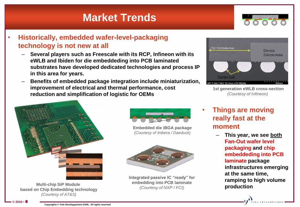
Market Trends
• Historically, embedded wafer-level-packaging
technology is not new at all– Several players such as Freescale with its RCP, Infineon with its
eWLB and Ibiden for die embeddeding into PCB laminated
substrates have developed dedicated technologies and process IP
in this area for years.
– Benefits of embedded package integration include miniaturization,
improvement of electrical and thermal performance, cost
reduction and simplification of logistic for OEMs1st generation eWLB cross-section
(Courtesy of Infineon)
Integrated passive IC “ready” for
embedding into PCB laminate
(Courtesy of NXP / FCI)
• Things are moving
really fast at the
moment– This year, we see both
Fan-Out wafer level
packaging and chip
embeddeding into PCB
laminate package
infrastructures emerging
at the same time,
ramping to high volume
production
Embedded die iBGA package(Courtesy of Imbera / Daeduck)
Multi-chip SiP Module
based on Chip Embedding technology(Courtesy of AT&S)

© 2010 • 9Copyrights © Yole Développement SARL. All rights reserved.
Fan-out WLP Concept
• A new SiP-friendly package platform processed at the wafer / panel level
with built-in substrate routing.

© 2010 • 10Copyrights © Yole Développement SARL. All rights reserved.
Audio Amplifiers
Operational Amplifiers
MEMS (RF, Silicon-
microphones…)
Headphones drivers
Temperature sensors
MOSFET
WL-CSP Applications Space
I/Os5 10 > 50 >100
IPD for ESD/EMI
LED Drivers
MEMS inertials (gyroscopes, accelerometers)
Logic / analog parts
CMOS image sensors
Wireless RF chips:
- GPS + Bluetooth
- FM radio
Logic Basebands
RF connectivity
Multi-Mode
Transceivers
PMUs
200-350
FOWLP is
extending WLP
application
space to higher
pin counts ICs:
> 110 - 300 I/Os

© 2010 • 11Copyrights © Yole Développement SARL. All rights reserved.
Fan-Out WLP technology is emerging on both 200mm / 300mm infrastructures
• Infineon is having a great sucess with its proprietary eWLB technology– The first FO-WLP eWLB wafers are mass produced on 200mm both Infineon (GE), ASE (TW) and
StatschippaC (SG) since 2009.
– Indeed, Fan-Out WLP is extending the general concept of Wafer Scale Packaging to new application
categories, especially the ones with higher pin-counts and larger chip size such as wireless
communication ICs
• First embedded wafer-level-package products based on eWLB have been
identified within LGE and Nokia handsets
– This year, a few additional players
are even more aggressive in
putting further capacity for eWLB
manufacturing as both
StatschippaC (SG) and NANIUM
(PT) are at the moment ramping-
up their facilities for
manufacturing the first generation
eWLB of Infineon on 300mm
reconfigured wafers
– Other packaging houses such as
SPIL, Amkor, UTAC and others
are also on the point to announce
the start of their own Fan-out
wafer level packaging operations
300mm eWLB reconfigured wafer (Courtesy of NANIUM)

© 2010 • 12Copyrights © Yole Développement SARL. All rights reserved.
Embedded die package technology to expand fast from niche to high volume markets
• At the same time, embedded die package technology has made a lot of progress on its side !
– Based on PCB laminate infrastructure, chip embeddeding technology is actually on the way to catch a
relatively important portion of the actual „Fan-in‟ WLCSP packaging business as it does leverage the
existing WLP/RDL infrastructure already established worldwide: indeed, most of WLCSP die applications are
“embedded ready”, so to realize the full benefits of this “WLCSP to Embedded die” conversion, only a few
extra manufacturing steps are missing like the realization of thin copper plating process, extreme wafer
thinning down to 50μm, thin dies handling and dicing.
• Electrical performance, testing and manufacturing yields are still major issues and
showstoppers for chip embedding technology to move forward
– Therefore, initial volume markets for embedded packages will be rather small, low pin-counts analog type of
applications such as integrated passive devices (IPD), RFID and power MOSFET components that are at the
moment under qualification for mass production before the end of this year already.
– Generally speaking, we believe that the winning situation for embedded die packages can be met for
company partnerships able to cross-over the traditional packaging, assembly and test supply chain. A good
example would be to put together a leading analog IC player (such as TI, Maxim IC, NXP or ST) with a
WLP/RDL partner (such as FCI, Casio Micronics, NEPES, etc…) together with a PCB integrator player (such
as Imbera / Daeduck, Ibiden, AT&S, Taiyo Yuden or SEMCO). This type of emerging partnerships are
absolutely necessary in order to standardize the embedded package technology and to leverage an entire
new packaging infrastructure based on low-cost, panel size PCB manufacturing techniques.
iBGA embedded die wafer-level-package cross-section (Courtesy of Imbera / Daeduck)
© 2010 • 13Copyrights © Yole Développement SARL. All rights reserved.
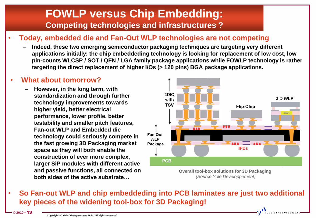
FOWLP versus Chip Embedding:Competing technologies and infrastructures ?
• Today, embedded die and Fan-Out WLP technologies are not competing– Indeed, these two emerging semiconductor packaging techniques are targeting very different
applications initially: the chip embeddeding technology is looking for replacement of low cost, low
pin-counts WLCSP / SOT / QFN / LGA family package applications while FOWLP technology is rather
targeting the direct replacement of higher I/Os (> 120 pins) BGA package applications.
• So Fan-out WLP and chip embeddeding into PCB laminates are just two additional
key pieces of the widening tool-box for 3D Packaging!
• What about tomorrow?– However, in the long term, with
standardization and through further
technology improvements towards
higher yield, better electrical
performance, lower profile, better
testability and smaller pitch features,
Fan-out WLP and Embedded die
technology could seriously compete in
the fast growing 3D Packaging market
space as they will both enable the
construction of ever more complex,
larger SiP modules with different active
and passive functions, all connected on
both sides of the active substrate…Overall tool-box solutions for 3D Packaging
(Source Yole Developpement)

© 2010 • 14Copyrights © Yole Développement SARL. All rights reserved.
Current / Future Tool-Box for 3D Packaging
30mm2 50mm2 80mm2 100mm2 500mm2
Chip /
Package
Size
I/O
. Count
5
50
120
300
500
15
2mm2
> 1 000
Logic
eFlasheDRAMAnalog
InterposerRF + I/Os
WLP
Fan-in
MEMS
WLP
PoP High Density
FOWLP - PoP
Logic
3-D SOC
3D Silicon PoP
3-D Logic SiP
3-D
RF-SiP
3-D Flip-Chip
PoP ‟Bottom Package‟ evolution:
Face to Face
TMV
FO WLP - SiP
FOWLP
Embedded Die
Embedded MCP Module
TSVSilicon/Glass
WLP Embedded BGA/PoP
FO WLP - MCP

© 2010 • 15Copyrights © Yole Développement SARL. All rights reserved.
Embedded Wafer-Level-Package technologies
Fan-out WLP
• Wafers or panels are
(re)configured
– By placing known good ICs active
face down on a foil and by over-
molding them
– These wafers/panels are then
flipped and processed back in the
wafer fab with RDL, bumping, …
Chip embedding (or embedded IC in PCB)
• Known good ICs and picked
– and placed on top of an organic
layer of Printed circuit board
– Subsequent layers are laminated
on top and regular PCB
manufacturing operations take
place on the panel with the
embedded ICs
Both these technologies are considered (n+1) technologies versus
WLCSP. Among others, they offer the following differential benefits:
fan-out area for larger IO densities than WLCSP
Collective wafer level processing of known good dice (KGD)
Higher expected second level reliability (package connection to the
mother board)
Back-side protection
System-in-package and 3D integration capabilities
Embedded
IC in PCBFO-WLP

© 2010 • 16Copyrights © Yole Développement SARL. All rights reserved.
Some more slides extracted from the Report …

© 2010 • 17Copyrights © Yole Développement SARL. All rights reserved.
About the Authors of this Report
• Jean-Marc Yannou
– Jean-Marc recently joined Yole Développement as technology and
market expert in the fields of advanced packaging and Integrated
Passive Devices. He has 15-years of experience in the
semiconductor industry. He worked for Texas Instruments and
Philips (then NXP semiconductors) where he served as
“Innovation Manager” for System-in-Package technologies
Contact: [email protected]
• Jerome Baron
– Jerome is leading the MEMS & Advanced Packaging market
research at Yole Developpement. He is leading the MEMS and
Advanced Packaging market research at Yole. He has been
involved in the technology analysis of the 3D packaging market
evolution at device, equipment and material supplier levels. He
was granted a Master of Science degree in Nanotechnologies from
the National Institute of Applied Sciences in Lyon, France
Contact: [email protected]

© 2010 • 18Copyrights © Yole Développement SARL. All rights reserved.
How to stay connected in the Advanced Packaging area with us?
www.i-micronews.com/3DIC.asp
Market Research Reports &Strategy Consulting Services
Publications & Newsletters
Wafer Level Packaging2009 Report
www.yole.fr

© 2010 • 19Copyrights © Yole Développement SARL. All rights reserved.
What about on-site workshops?
• Off-the-shelf Reports will never meet all your expectations because
they are inherently built to cover a wide range of applications,
markets, technologies and players
• Our analysts also have the possibility to prepare presentations and
on-site workshops at your company place for:
– De-briefing your team on several specific topics described within the report
– Prepare a face to face Q&A session: your company‟s experts send a list of
questions in advance. Based on this list, our analysts can elaborate a „more
focused‟ analysis and presentation on what really matters for you!
For more information about the possible
organization of workshops with Yole‟s
analysts, please contact us.