
Electromagnetic compatibility of Integrated · PDF fileElectromagnetic compatibility of...
63
19/01/2017 1 January 17 Electromagnetic compatibility of Integrated Circuits Jan. 2017 www.etienne-sicard.fr > Teaching > EMC of ICs Etienne SICARD INSA/DGEI University of Toulouse 31077 Toulouse - France [email protected] Alexandre BOYER INSA/DGEI – LAAS-CNRS University of Toulouse 31077 Toulouse - France [email protected] 2 January 17 Objectives Through lectures (6 H) Understand parasitic emission mechanisms Introduce parasitic emission reduction strategies Give an overview of emission and susceptibility measurement standards Power Decoupling Network modelling Basis of conducted and radiated emission modelling Basis of immunity modelling Understand the role of decoupling at printed-circuit-board level Acquire basic knowledge of design for improved EMC at PCB and IC level Through practical training (12 H) Illustrate basic concepts through simulation IC modeling case study Evaluation based on report
Transcript of Electromagnetic compatibility of Integrated · PDF fileElectromagnetic compatibility of...

19/01/2017
1 January 17
Electromagnetic compatibility of Integrated Circuits
Jan. 2017
www.etienne-sicard.fr > Teaching > EMC of ICs
Etienne SICARDINSA/DGEIUniversity of Toulouse31077 Toulouse - [email protected]
Alexandre BOYERINSA/DGEI – LAAS-CNRSUniversity of Toulouse31077 Toulouse - [email protected]
2 January 17
Objectives
Through lectures (6 H) Understand parasitic emission mechanisms Introduce parasitic emission reduction strategies Give an overview of emission and susceptibility measure ment
standards Power Decoupling Network modelling Basis of conducted and radiated emission modelling Basis of immunity modelling Understand the role of decoupling at printed-circui t-board level Acquire basic knowledge of design for improved EMC at PCB and IC
level
Through practical training (12 H) Illustrate basic concepts through simulation IC modeling case study
Evaluation based on report
19/01/2017
3 January 17
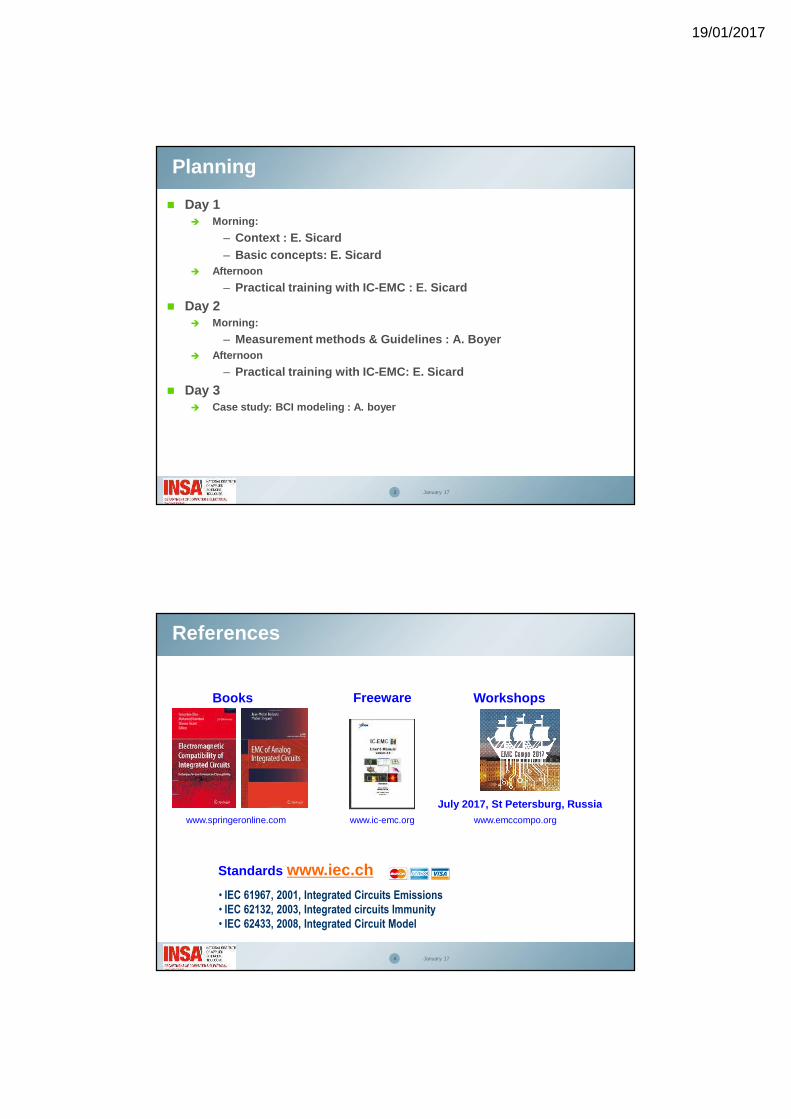
Planning
Day 1 Morning:
– Context : E. Sicard– Basic concepts: E. Sicard
Afternoon
– Practical training with IC-EMC : E. Sicard
Day 2 Morning:
– Measurement methods & Guidelines : A. Boyer Afternoon
– Practical training with IC-EMC: E. Sicard
Day 3 Case study: BCI modeling : A. boyer
References
4 January 17
Books
www.springeronline.com www.ic-emc.org
Freeware
www.emccompo.org
Workshops
Standards www.iec.ch
• IEC 61967, 2001, Integrated Circuits Emissions
• IEC 62132, 2003, Integrated circuits Immunity
• IEC 62433, 2008, Integrated Circuit Model
July 2017, St Petersburg, Russia
19/01/2017
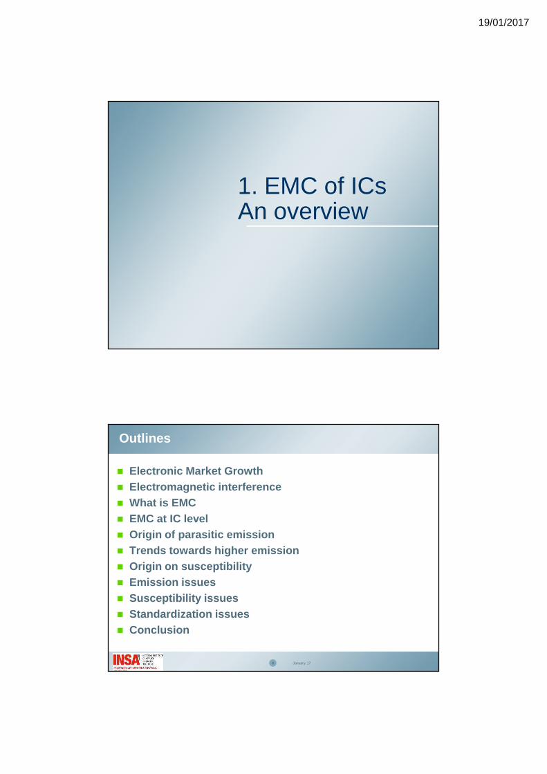
1. EMC of ICsAn overview
Outlines
Electronic Market Growth Electromagnetic interference What is EMC EMC at IC level Origin of parasitic emission Trends towards higher emission Origin on susceptibility Emission issues Susceptibility issues Standardization issues Conclusion
6 January 17
19/01/2017
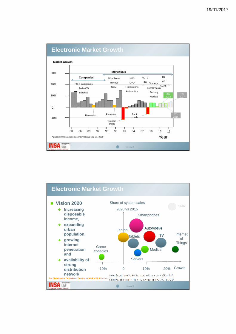
Electronic Market Growth
7 January 17
83 86 89 92 95 98 01 04
-10%
0
10%
Adapted from Electronique International Mai 21, 2009 Year
07
20% PC in companies
Audio CD
Defense
Companies
10
30%
13 16
Individuals
Society
PC at home
Internet
GSM
MP3
DVD
Flat screens
AutomotiveLocal Energy
Security
Medical
Telecom crash
Bank crash
HDTV
3G
4G
IoT
ADAS
3%2015
Recession Recession
3%2014
4%2017
Market Growth
Electronic Market Growth
Vision 2020 Increasing
disposable income,
expanding urban population,
growing internet penetration and
availability of strong distribution network
8 January 17
0 10% 20%-10%
Share of system sales
2020 vs 2015
Smartphones
Game consoles Medical
Internet of
Things
Laptop
Tablets
Servers
Growth
100B$
19/01/2017
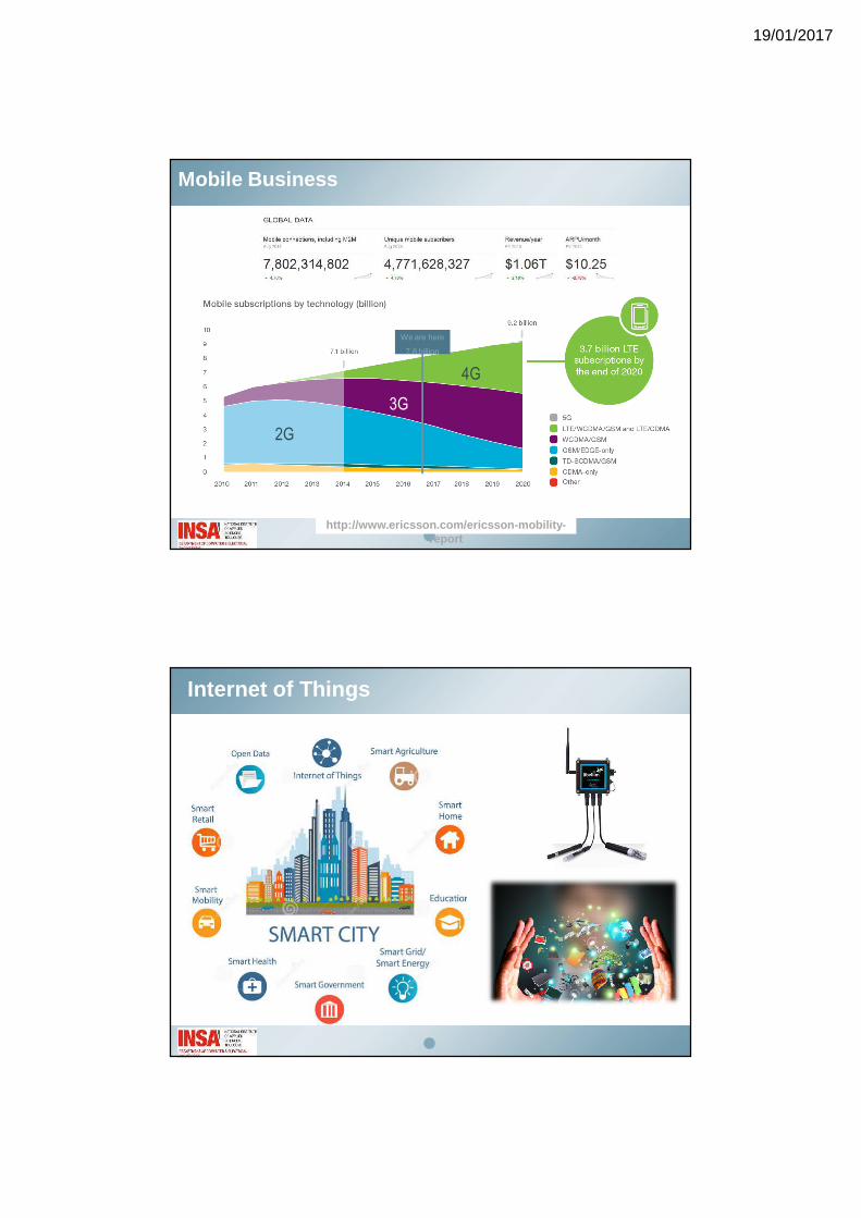
Mobile Business
http://www.ericsson.com/ericsson-mobility-report
We are here
7.8 billion
2G
3G
4G
Internet of Things
19/01/2017
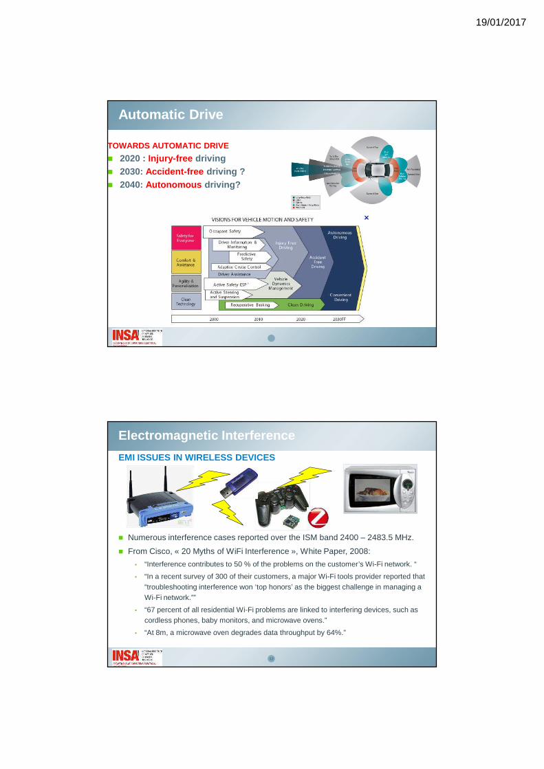
Automatic Drive
TOWARDS AUTOMATIC DRIVE
2020 : Injury-free driving 2030: Accident-free driving ? 2040: Autonomous driving?
12
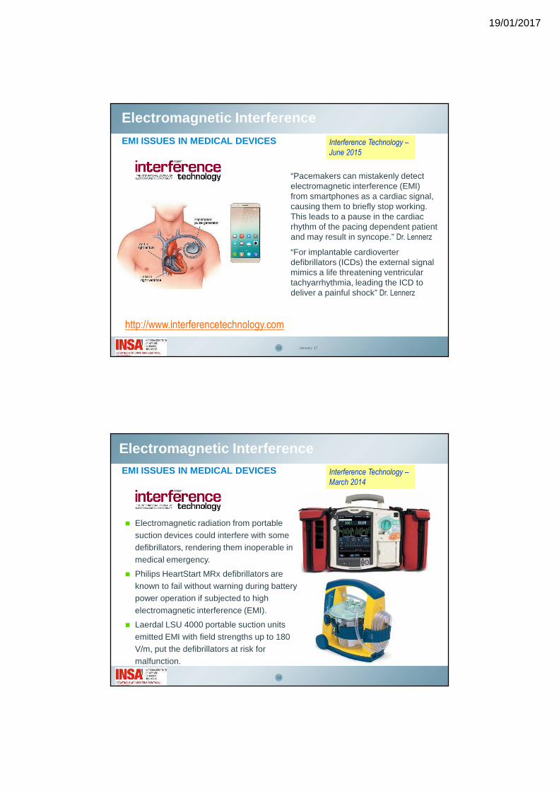
EMI ISSUES IN WIRELESS DEVICES
Numerous interference cases reported over the ISM band 2400 – 2483.5 MHz.
From Cisco, « 20 Myths of WiFi Interference », White Paper, 2008:
• “Interference contributes to 50 % of the problems on the customer’s Wi-Fi network. “
• “In a recent survey of 300 of their customers, a major Wi-Fi tools provider reported that “troubleshooting interference won ‘top honors’ as the biggest challenge in managing a Wi-Fi network.””
• “67 percent of all residential Wi-Fi problems are linked to interfering devices, such as cordless phones, baby monitors, and microwave ovens.”
• “At 8m, a microwave oven degrades data throughput by 64%.”
Electromagnetic Interference
19/01/2017
Electromagnetic Interference
13 January 17
“Pacemakers can mistakenly detect electromagnetic interference (EMI) from smartphones as a cardiac signal, causing them to briefly stop working. This leads to a pause in the cardiac rhythm of the pacing dependent patient and may result in syncope.” Dr. Lennerz
“For implantable cardioverter defibrillators (ICDs) the external signal mimics a life threatening ventricular tachyarrhythmia, leading the ICD to deliver a painful shock” Dr. Lennerz
EMI ISSUES IN MEDICAL DEVICES Interference Technology –
June 2015
http://www.interferencetechnology.com
Electromagnetic Interference
14
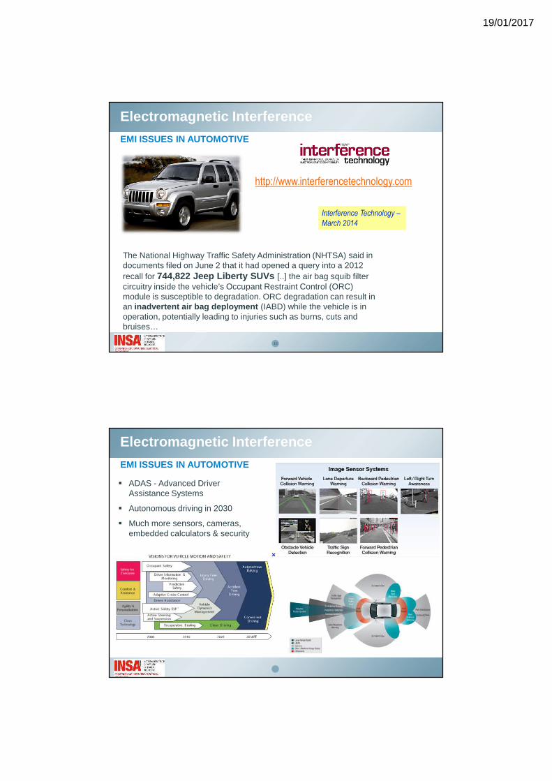
EMI ISSUES IN MEDICAL DEVICES
Electromagnetic radiation from portable suction devices could interfere with some defibrillators, rendering them inoperable in a medical emergency.
Philips HeartStart MRx defibrillators are known to fail without warning during battery power operation if subjected to high electromagnetic interference (EMI).
Laerdal LSU 4000 portable suction units emitted EMI with field strengths up to 180 V/m, put the defibrillators at risk for malfunction.
Interference Technology –
March 2014
19/01/2017
Electromagnetic Interference
15
EMI ISSUES IN AUTOMOTIVE
Interference Technology –
March 2014
The National Highway Traffic Safety Administration (NHTSA) said in documents filed on June 2 that it had opened a query into a 2012 recall for 744,822 Jeep Liberty SUVs [..] the air bag squib filter circuitry inside the vehicle’s Occupant Restraint Control (ORC) module is susceptible to degradation. ORC degradation can result in an inadvertent air bag deployment (IABD) while the vehicle is in operation, potentially leading to injuries such as burns, cuts and bruises…
http://www.interferencetechnology.com
ADAS - Advanced Driver Assistance Systems
Autonomous driving in 2030
Much more sensors, cameras, embedded calculators & security
EMI ISSUES IN AUTOMOTIVE
Electromagnetic Interference
19/01/2017
Electromagnetic Interference
17
EMI ISSUES IN AVIATION
FAA said Wi-Fi systems may interfere with the Honeywell phase 3 display units aboard 157 Boeing airplanes in use by various U.S. airlines. These display units are critical for flight safety, providing crewmembers with information such as airspeed, altitude, heading, and pitch and roll [..] the issue was discovered two years ago during testing to certify a Wi-Fi system for use on Boeing 737 Next Generation.
Interference Technology –
January 2013
Electromagnetic Interference
18
EMI ISSUES IN AVIATION
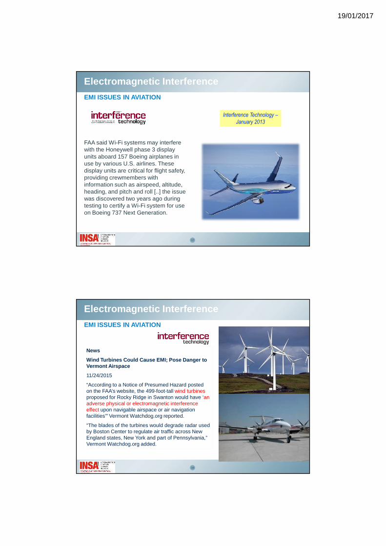
News
Wind Turbines Could Cause EMI; Pose Danger to Vermont Airspace
11/24/2015
“According to a Notice of Presumed Hazard posted on the FAA’s website, the 499-foot-tall wind turbines proposed for Rocky Ridge in Swanton would have ‘an adverse physical or electromagnetic interference effect upon navigable airspace or air navigation facilities’” Vermont Watchdog.org reported.
“The blades of the turbines would degrade radar used by Boston Center to regulate air traffic across New England states, New York and part of Pennsylvania,” Vermont Watchdog.org added.
19/01/2017
What is EMC
19
« The ability of a component, equipment or system to operate satisfyingly in a given electromagnetic environment, without introducing any harmful electromagnetic disturbances to all systems placed in this environment. »
Essential constraint to ensure functional safety of electronic or electrical applications
Guarantee the simultaneous operation of every electrical or electronic equipment in a given electromagnetic environment
Reduce both the parasitic electromagnetic emission and the sensitivity or susceptibility to electromagnetic interferences.
DEFINITION
EMC at IC level
20 January 17
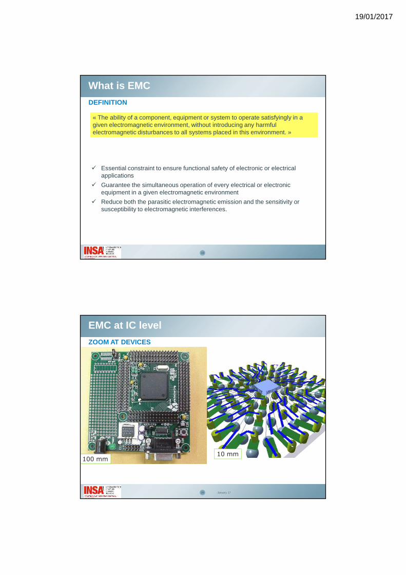
100 mm10 mm
ZOOM AT DEVICES
19/01/2017
21 January 17
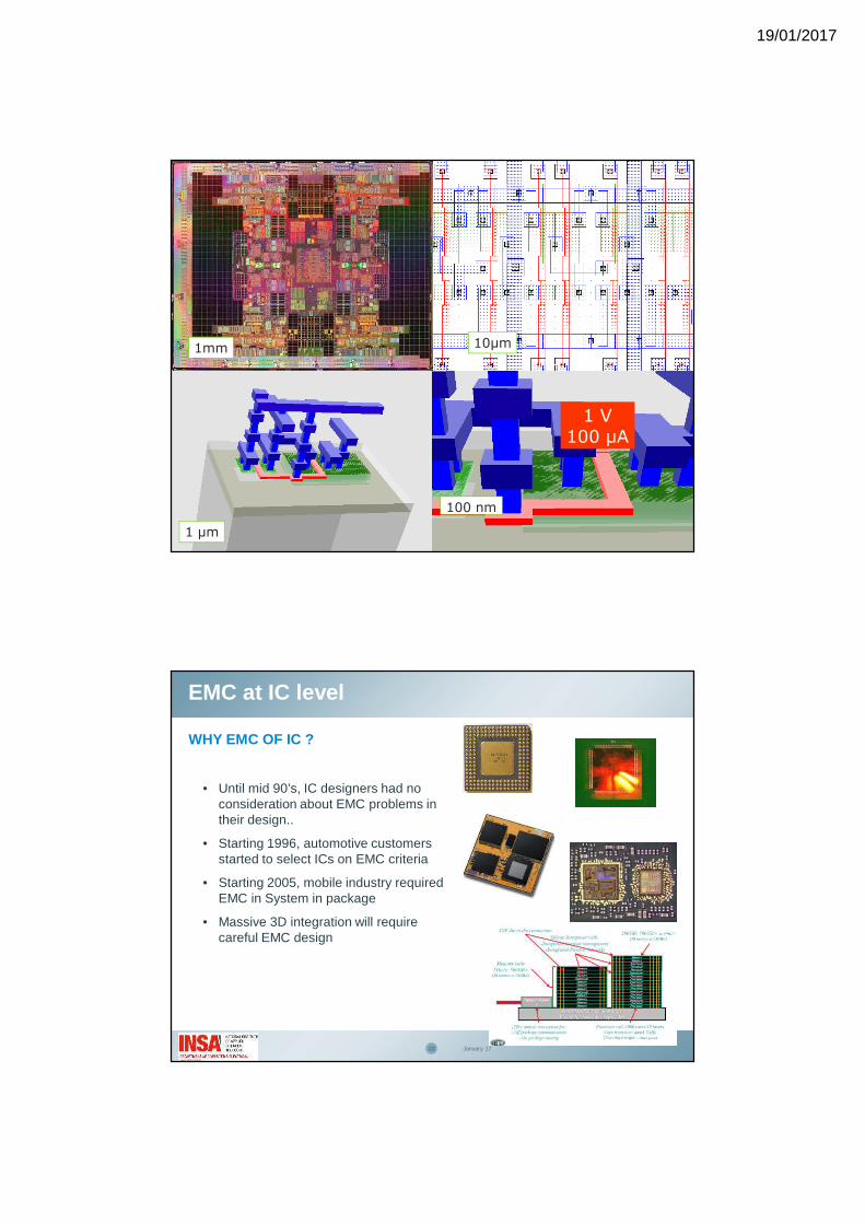
Integrated Circuits…
© Intel Xeon1 µm
100 nm
1 V100 µA
10µm1mm
EMC at IC level
22 January 17
WHY EMC OF IC ?
• Until mid 90’s, IC designers had no consideration about EMC problems in their design..
• Starting 1996, automotive customers started to select ICs on EMC criteria
• Starting 2005, mobile industry required EMC in System in package
• Massive 3D integration will require careful EMC design
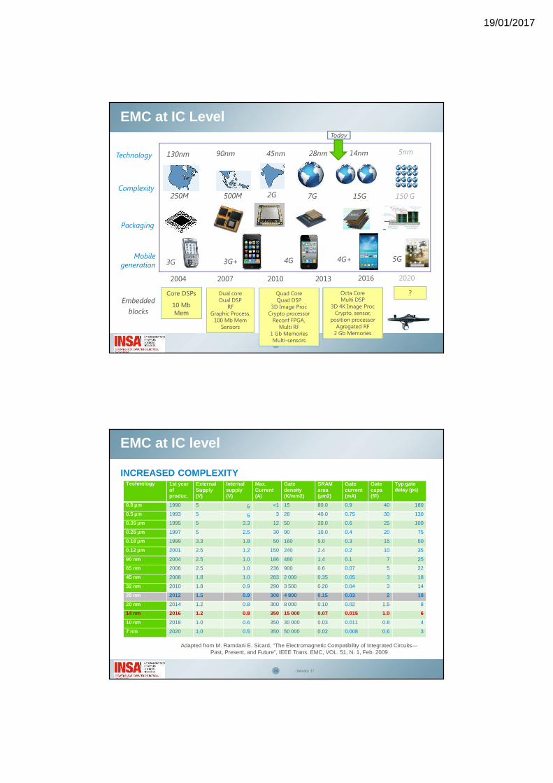
19/01/2017
Technology
Complexity
Packaging
2004
130nm
Embedded
blocks
2007
90nm
250M
Core DSPs
10 Mb Mem
2010
45nm
500M
Dual coreDual DSP
RFGraphic Process.
100 Mb MemSensors
2013
28nm
2G
Quad CoreQuad DSP
3D Image ProcCrypto processor
Reconf FPGA, Multi RF
1 Gb MemoriesMulti-sensors
7G
Mobile generation 3G 3G+ 4G
5nm
150 G
2020
?
5G
EMC at IC Level
14nm
2016
4G+
Today
Octa CoreMulti DSP
3D 4K Image ProcCrypto, sensor,
position processorAgregated RF
2 Gb Memories
15G
EMC at IC level
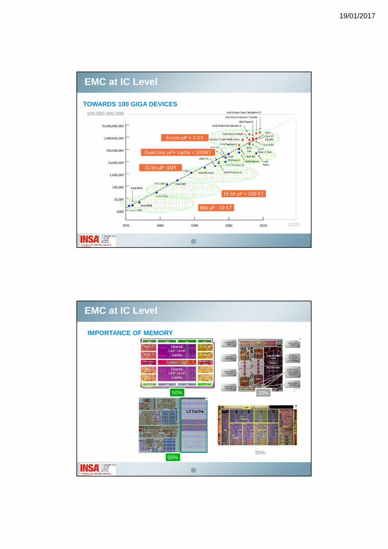
24 January 17
Technology 1st year of produc.
External Supply (V)
Internal supply (V)
Max. Current (A)
Gate density (K/mm2)
SRAM area (µm2)
Gate current (mA)
Gate capa (fF)
Typ gate delay (ps)
0.8 µm 1990 5 5 <1 15 80.0 0.9 40 180
0.5 µm 1993 5 5 3 28 40.0 0.75 30 130
0.35 µm 1995 5 3.3 12 50 20.0 0.6 25 100
0.25 µm 1997 5 2.5 30 90 10.0 0.4 20 75
0.18 µm 1999 3.3 1.8 50 160 5.0 0.3 15 50
0.12 µm 2001 2.5 1.2 150 240 2.4 0.2 10 35
90 nm 2004 2.5 1.0 186 480 1.4 0.1 7 25
65 nm 2006 2.5 1.0 236 900 0.6 0.07 5 22
45 nm 2008 1.8 1.0 283 2 000 0.35 0.05 3 18
32 nm 2010 1.8 0.9 290 3 500 0.20 0.04 3 14
28 nm 2012 1.5 0.9 300 4 800 0.15 0.03 2 10
20 nm 2014 1.2 0.8 300 8 000 0.10 0.02 1.5 8
14 nm 2016 1.2 0.8 350 15 000 0.07 0.015 1.0 6
10 nm 2018 1.0 0.6 350 30 000 0.03 0.011 0.8 4
7 nm 2020 1.0 0.5 350 50 000 0.02 0.008 0.6 3
INCREASED COMPLEXITY
Adapted from M. Ramdani E. Sicard, “The Electromagnetic Compatibility of Integrated Circuits—Past, Present, and Future”, IEEE Trans. EMC, VOL. 51, N. 1, Feb. 2009
19/01/2017
8bit µP : 10 KT
16 bit µP = 100 KT
32 bit µP :1MT
Dual core µP+ cache = 100MT
8-core µP = 2 GT
TOWARDS 100 GIGA DEVICES
2020
100,000,000,000
EMC at IC Level
50% 20%
55%35%
EMC at IC Level
IMPORTANCE OF MEMORY
19/01/2017
EMC at IC level
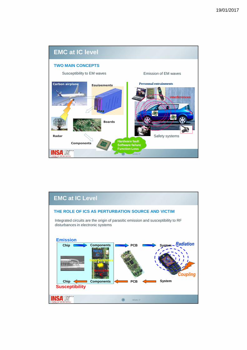
27 January 17
Emission of EM wavesSusceptibility to EM waves
TWO MAIN CONCEPTS
Personnal entrainments
Safety systems
interferences
Hardware faultSoftware failureFunction Loss
Components
EquipementsCarbon airplane
Boards
Radar
28 January 17
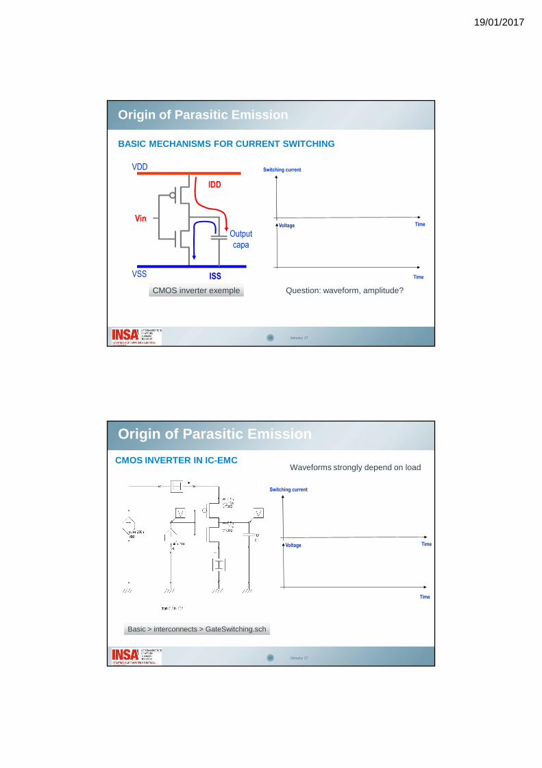
Susceptibility
Chip
Chip
EmissionPCB
PCB System
Components
Components
System
Integrated circuits are the origin of parasitic emission and susceptibility to RF disturbances in electronic systems
Noisy IC
Sensitive IC
Interferences
THE ROLE OF ICS AS PERTURBATION SOURCE AND VICTIM
Radiation
Coupling
EMC at IC Level
19/01/2017
29 January 17
VDD
VSS
Output capa
Vin
Origin of Parasitic Emission
BASIC MECHANISMS FOR CURRENT SWITCHING
IDD
ISS
Switching current
Voltage Time
Time
Question: waveform, amplitude?CMOS inverter exemple
Origin of Parasitic Emission
30 January 17
Basic > interconnects > GateSwitching.sch
CMOS INVERTER IN IC-EMC
Switching current
Voltage Time
Time
Waveforms strongly depend on load
19/01/2017
31 January 17
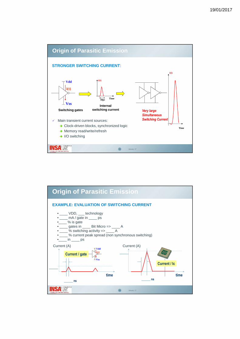
Origin of Parasitic Emission
STRONGER SWITCHING CURRENT:
50ps
i(t)
Time
Switching gatesInternal
switching current
Vdd
Vss
i(t)
Main transient current sources: Clock-driven blocks, synchronized logic Memory read/write/refresh I/O switching
Very large
Simultaneous
Switching Current
i(t)
Time
Origin of Parasitic Emission
32 January 17
EXAMPLE: EVALUATION OF SWITCHING CURRENT
• ____ VDD, ___ technology• ____ mA / gate in ____ ps•____ % is gate• ____ gates in ____ Bit Micro => ____ A• ____ % switching activity => ____ A• ____ % current peak spread (non synchronous switching) •____ in ____ ps
____
Current (A)
____ ns
time
Vdd
Vss
i(t)Current / gate
Current (A)
____ ns
time
Current / Ic
____
19/01/2017
Origin of Parasitic Emission
33 January 17
Vss
Vdd
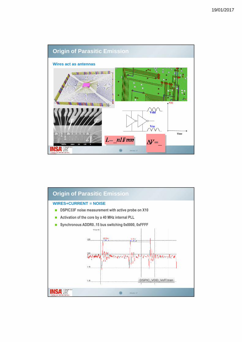
Wires act as antennas
V(t)
Time
Origin of Parasitic Emission
34 January 17
WIRES+CURRENT = NOISE
DSPIC33F noise measurement with active probe on X10
Activation of the core by a 40 MHz internal PLL
Synchronous ADDR0..15 bus switching 0x0000, 0xFFFF
DSPIC_VDD_VofT.tran
19/01/2017
Origin of Parasitic Emission
35 January 17
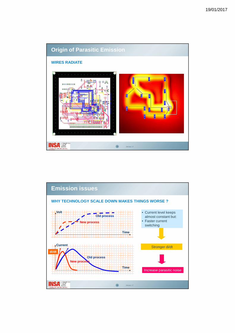
WIRES RADIATE
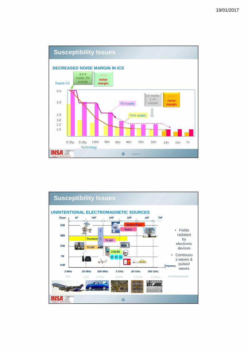
Emission issues
36 January 17
Stronger di/dtStronger di/dt
Increase parasitic noiseIncrease parasitic noise
Time
New process
VoltOld process
WHY TECHNOLOGY SCALE DOWN MAKES THINGS WORSE ?
• Current level keepsalmost constant but:
• Faster currentswitching
• Current level keepsalmost constant but:
• Faster currentswitching
Time
Current
di/dt
New processOld process
19/01/2017
Susceptibility Issues
37 January 17
DECREASED NOISE MARGIN IN ICS
5.0
3.3
2.5
1.8
0.35µ 0.18µ 90n 65n
Technology
1.0
Supply (V)
1.2
45n
I/O supply
Core supply
32n 20n 14n130n
3.3 V inside, 5V outside
1V inside, 1.2V
outside
10n 7n
____
noise margin
____
noise margin
Thunderstorm impact
UNINTENTIONAL ELECTROMAGNETIC SOURCES
TV UHF
Radars
2-4G BS
1W
Frequency
1MW
1KW
1GW Weather Radar
3 MHz 30 MHz 300 MHz 3 GHz 30 GHz 300 GHz
Power
1mW
HF VHF UHF SHF xHF THF
3G
TV VHF
2G4G
• Fields radiated
by electronic devices
• Continuous waves &
pulsed waves
25m 25mm0.25m 2.5mm2.5m λλ/4 (ideal antenna)0.25mm
Susceptibility Issues
19/01/2017
39 January 17
EMC Level
(dB)
-40
-30
-20
-10
0
10
20
30
40
50
1 10 100 1000
Sum of
perturbations
Susceptibility
levelHigh risk of
interference
Safe
interference
margin
Unsafe margin
Frequency (MHz)
Susceptibility Issues
SYSTEM-ON-CHIP, 3D STACKING: DANGER
Conclusion
EMI reported in all kinds of devices IC involved in many EMI problems IC technology evolution towards
higher complexity On-chip switching currents in the
10-100 A range ICs are good antennas in the GHz
range Increased switching noise Increased emission issues Reduced noise margins System-on-chips, systems-in-
package rise new EMC issues
40 January 17
19/01/2017
2. EMC Basics concepts
42 January 17
1. Basic Principles
2. Specific Units
3. Radiating element
4. Emission Spectrum
5. Susceptibility Spectrum
6. Notion of margin
7. Impedance
8. Conclusion
Summary
19/01/2017
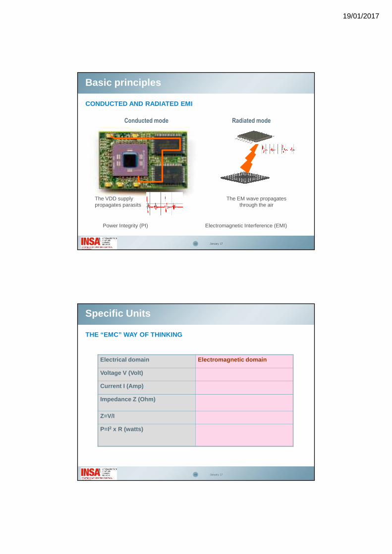
Basic principles
43 January 17
Radiated mode
The VDD supply propagates parasits
The EM wave propagates through the air
CONDUCTED AND RADIATED EMI
Conducted mode
Power Integrity (PI) Electromagnetic Interference (EMI)
44 January 17
Electrical domain Electromagnetic domain
Voltage V (Volt)
Current I (Amp)
Impedance Z (Ohm)
Z=V/I
P=I2 x R (watts)
Specific Units
THE “EMC” WAY OF THINKING
19/01/2017
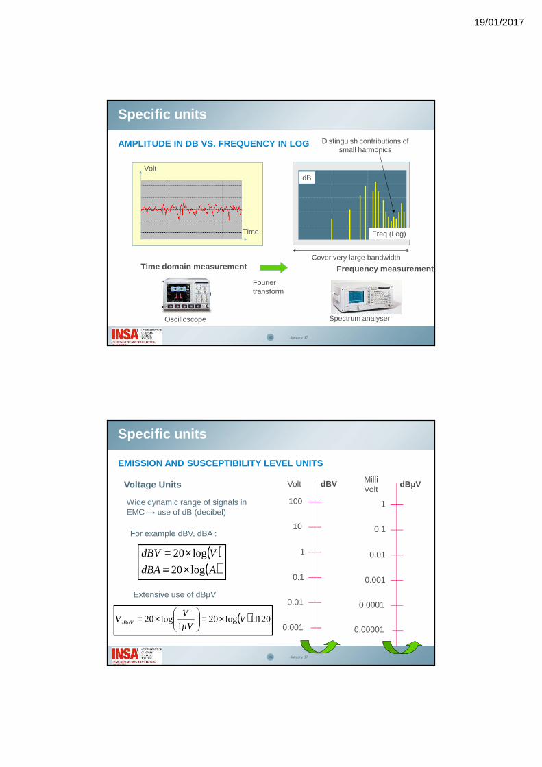
Specific units
45 January 17
Time domain measurement
Volt
Time
AMPLITUDE IN DB VS. FREQUENCY IN LOG
Oscilloscope
Frequency measurement
Fourier transform
Freq (Log)
dB
Spectrum analyser
Distinguish contributions of small harmonics
Cover very large bandwidth
Specific units
46 January 17
Voltage Units
Wide dynamic range of signals in EMC → use of dB (decibel)
0.1
10
1
100
0.01
Volt dBV
0.001
0.001
0.1
0.01
1
0.0001
MilliVolt
dBµV
0.00001
EMISSION AND SUSCEPTIBILITY LEVEL UNITS
For example dBV, dBA :
( )( )AdBA
VdBV
log20
log20
×=×=
Extensive use of dBµV
( ) 120log201
log20 +×=
×= V
µV
VVdBµV
19/01/2017
47 January 17
The most common power unit is the “dBm” (dB milli-Watt)
Power Units
1 mV = ___ dBµV
1 W = ___ dBm
Exercise: Specific units
Specific units
EMISSION AND SUSCEPTIBILITY LEVEL UNITS
( ) 30log101
log10 +×=
×= W
WdBmW P
mW
PP
1 W
1 MW
1 KW
Power(Watt)
1 mW
Power
(dBm)
1 µW
1 nW
IC-EMC: 0dbm in 50 Ω
Tools > dB/Unit converter
Radiating elements
48
RADIATED EMISSION
Y
Z
O
φ
θ R
X
Eθ
Hφ
Er
Io
rjor e
r
j
r
hIE β
ββθ
πηβ −
−=
3322
2 1cos
42
r
rjo er
j
r
j
r
hIE β
θ βββθ
πηβ −
−+=
3322
2 1sin
4
r
rjo er
jr
hIH β
ϕ ββθ
πβ −+= )
1
²²
1(sin
4
2r
0rrrr
=== θϕ HHE r
h
Elementary “Hertz” current dipole.
Short wire with a length << λ , crossedby a sinusoidal current with a constant amplitude Io
19/01/2017
Radiating elements
49 January 17
NEAR FIELD/FAR FIELD
πλβ2
1 <<⇒<< RRπλβ2
1 >>⇒>> RR
Close to the antenna Far from the antenna
πλ2lim =itR
Non radiating field (non TEM wave)
E and H decreases rapidly in 1/r³
Radiating field (TEM wave)
E and H decreases in 1/r
Near-field region
Far-field region
100 MHz : Rlimit =____
50 January 17
Specification
example for an IC
emission
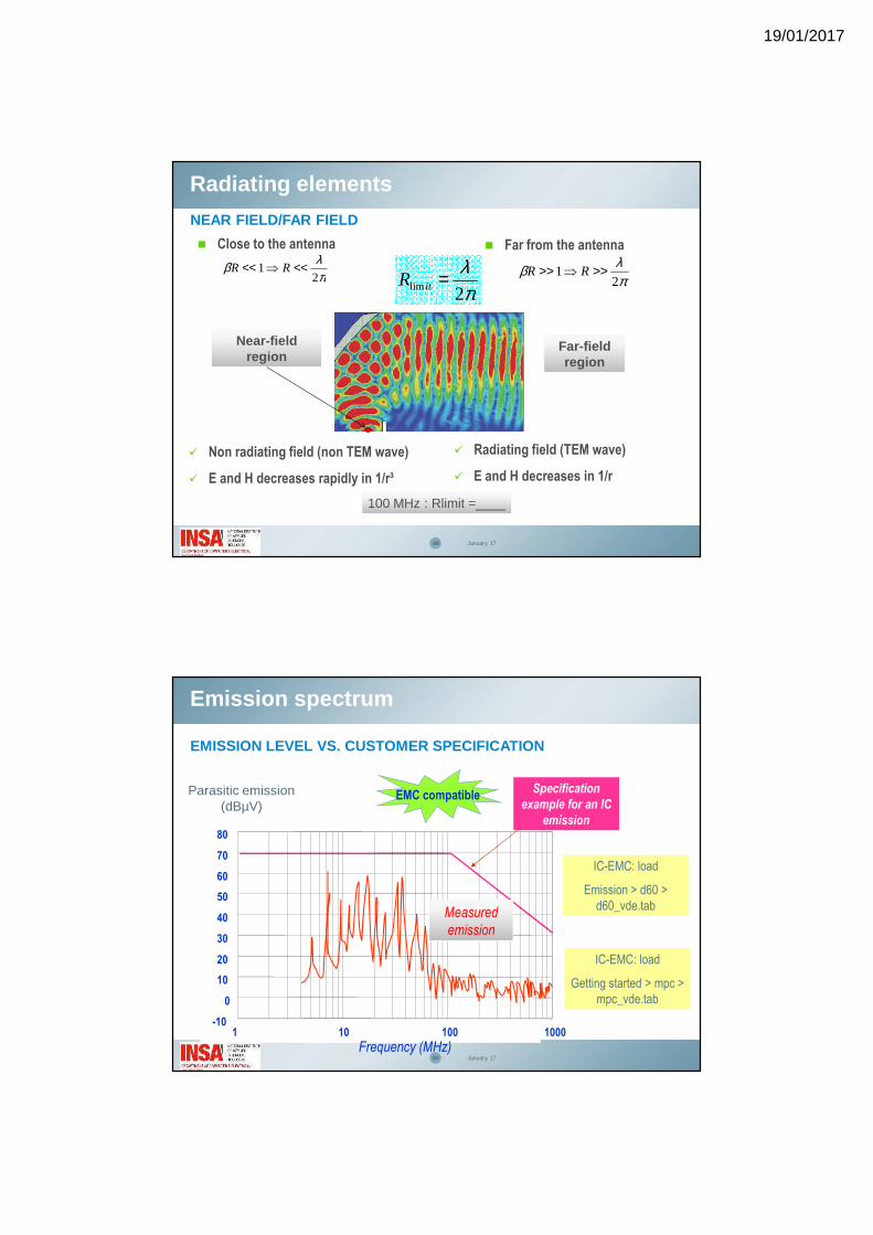
Parasitic emission (dBµV)
-10
0
10
20
30
40
50
60
70
80
1 10 100 1000
Frequency (MHz)
Measured
emission
EMC compatible
Emission spectrum
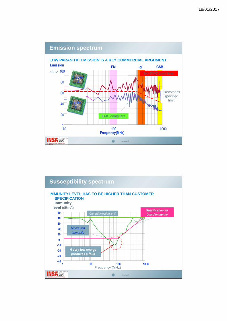
EMISSION LEVEL VS. CUSTOMER SPECIFICATION
IC-EMC: load
Emission > d60 > d60_vde.tab
IC-EMC: load
Getting started > mpc > mpc_vde.tab
19/01/2017
51 January 17
dBµV
0
20
40
60
80
100
10 100 1000
FM GSMRF
Supplier A
Supplier B
EMC compliant
Not EMC compliant
Frequency(MHz)
Customer's specified
limit
Emission spectrum
LOW PARASITIC EMISSION IS A KEY COMMERCIAL ARGUMENTEmission
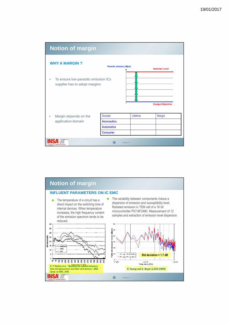
Susceptibility spectrum
52 January 17
Immunity level (dBmA)
-40
-30
-20
-10
0
10
20
30
40
50
1 10 100 1000
Specification for
board immunityCurrent injection limit
Measured
immunity
A very low energy
produces a fault
Frequency (MHz)
IMMUNITY LEVEL HAS TO BE HIGHER THAN CUSTOMER SPECIFICATION
19/01/2017
Notion of margin
53 January 17
WHY A MARGIN ?
Domain Lifetime Margin
Aeronautics
Automotive
Consumer
Parasitic emission (dBµV)Nominal Level
Design Objective
• To ensure low parasitic emission ICs supplier has to adopt margins
• Margin depends on the application domain
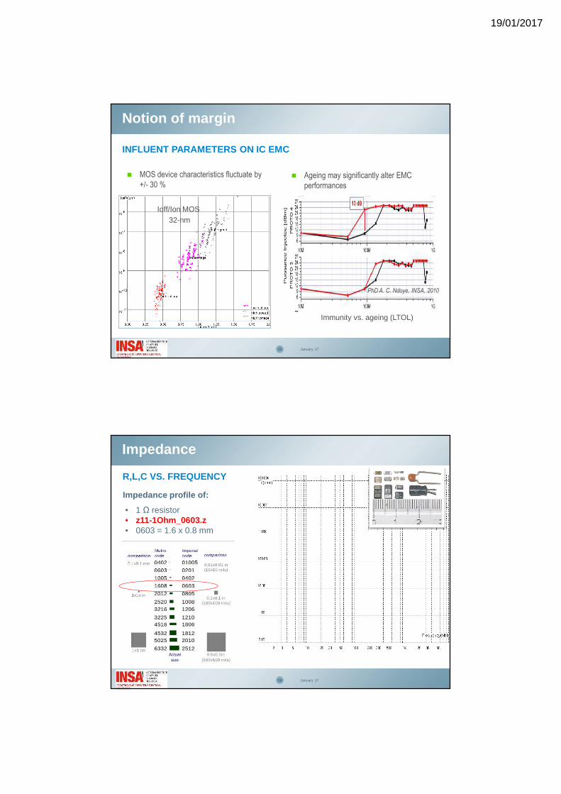
Notion of margin
54 January 17
INFLUENT PARAMETERS ON IC EMC
The temperature of a circuit has a direct impact on the switching time of internal devices. When temperature increases, the high frequency content of the emission spectrum tends to be reduced.
K. P. Slattery et al., “Modeling the radiated emissions
from microprocessors and other VLSI devices”, IEEE
Symp. on EMC, 2000.
The variability between components induce a dispersion of emission and susceptibility level. Radiated emission in TEM cell of a 16 bit microcontroller PIC18F2480. Measurement of 12 samples and extraction of emission level dispersion.
H. Huang and A. Boyer (LAAS-CNRS)
Std deviation = 1.7 dB
19/01/2017
Notion of margin
55 January 17
Ioff/Ion MOS 32-nm
PhD A. C. Ndoye, INSA, 2010
Immunity vs. ageing (LTOL)
INFLUENT PARAMETERS ON IC EMC
MOS device characteristics fluctuate by +/- 30 %
Ageing may significantly alter EMC performances
56 January 17
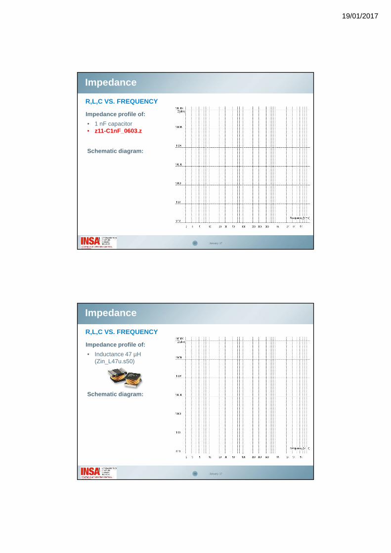
R,L,C VS. FREQUENCY
Impedance profile of:
Impedance
• 1 Ω resistor• z11-1Ohm_0603.z• 0603 = 1.6 x 0.8 mm
Schematic diagram:
19/01/2017
57 January 17
R,L,C VS. FREQUENCY
Impedance
• 1 nF capacitor • z11-C1nF_0603.z
Impedance profile of:
Schematic diagram:
58 January 17
R,L,C VS. FREQUENCY
Impedance
• Inductance 47 µH (Zin_L47u.s50)
Impedance profile of:
Schematic diagram:
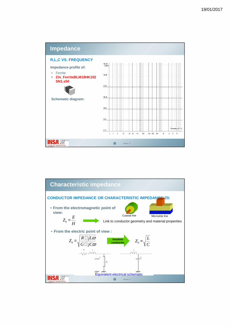
19/01/2017
59 January 17
R,L,C VS. FREQUENCY
Impedance
• Ferrite• Zin_FerriteBLM18HK102
SN1.s50
Impedance profile of:
Schematic diagram:
Characteristic impedance
60 January 17
CONDUCTOR IMPEDANCE OR CHARACTERISTIC IMPEDANCE Z0:
Coaxial line Microstrip line
• From the electromagnetic point of view:
H
EZ =0 Link to conductor geometry and material properties
ωω
jCG
jLRZ
++=0
C
LZ ≈0
losslessconductor
• From the electric point of view :
Equivalent electrical schematic
19/01/2017
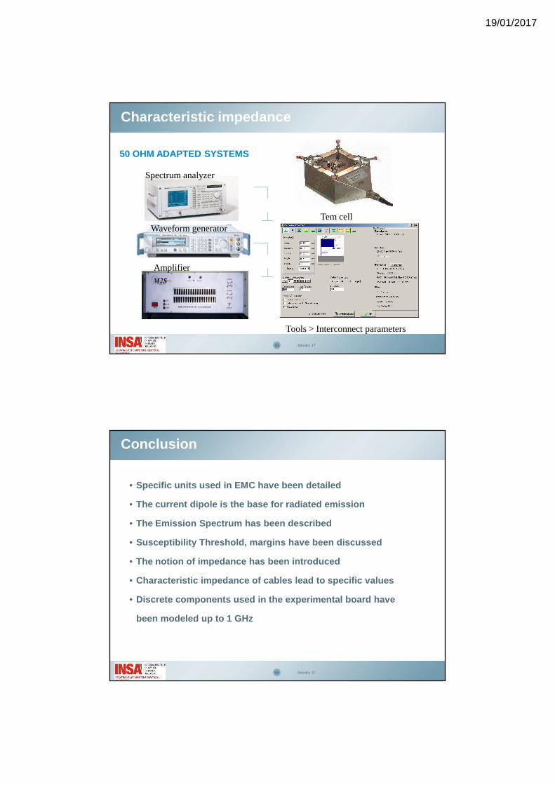
Characteristic impedance
61 January 17
IMPEDANCE MATCHING
Adapted:Not adapted:
time
Voltage
time
Voltage
Why impedance matching is fundamental ?
IC-EMC
Impedance>
impedance_mismatch.sch
Characteristic impedance
62 January 17
Small conductor Large conductor
What is the optimum characteristic impedance for a coaxial cable ?
CHARACTERISTIC IMPEDANCE Z0:
• Maximum power : Z0 = ___Ω
• Minimum loss: Z0 = ___ Ω
Small conductor
Large conductor
Power handling
Bending
weight
Low loss
Small capacitance
Small inductance
Low Impedance
Or ?
Ideal values:
• EMC cable (compromise between power and loss) : Z0 = ___ Ω
• TV cable : Z0 = ___ Ω
• Base station cable : Z0 = ___ Ω
Cable examples:
19/01/2017
Characteristic impedance
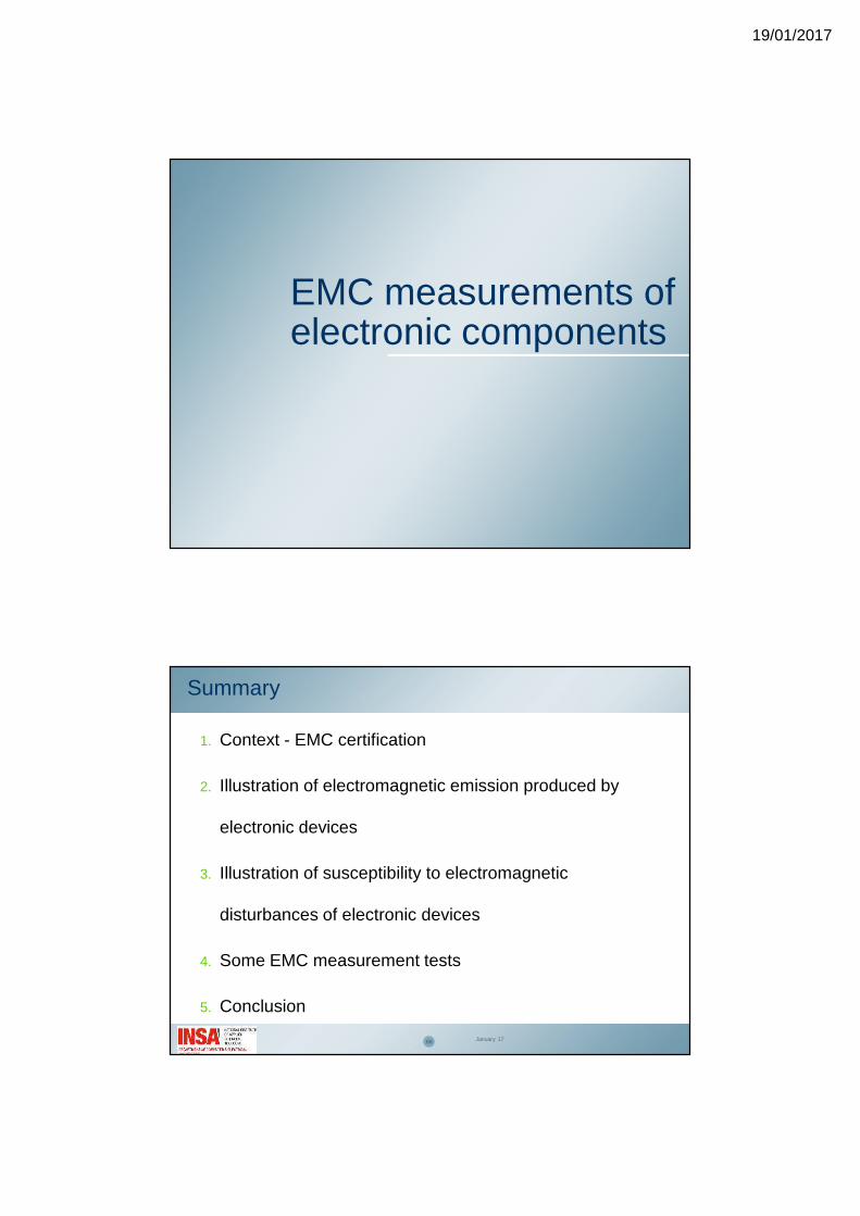
63 January 17
50 OHM ADAPTED SYSTEMS
Tem cell
Spectrum analyzer
Waveform generator
Amplifier
Tools > Interconnect parameters
64 January 17
• Specific units used in EMC have been detailed
• The current dipole is the base for radiated emissio n
• The Emission Spectrum has been described
• Susceptibility Threshold, margins have been discuss ed
• The notion of impedance has been introduced
• Characteristic impedance of cables lead to specific values
• Discrete components used in the experimental board have
been modeled up to 1 GHz
Conclusion
19/01/2017
EMC measurements of electronic components
66
Summary
1. Context - EMC certification
2. Illustration of electromagnetic emission produced by
electronic devices
3. Illustration of susceptibility to electromagnetic
disturbances of electronic devices
4. Some EMC measurement tests
5. Conclusion
January 17

19/01/2017
67
Context - The EMC certification
January 17
RED 2014/53/UE : for radio equipments
CEM 2014/30/UE : electromagnetic compatibility of electronic products
BT 2014/35/UE : electric safety for electronic products (0 to 1000 volt AC and 1500 DC)
RoHS 2011/65/UE : limitation of six hazardous substances (e.g. lead)
DEEE 2012/19/UE : management of electric and electronic equipment waste
European Directives for electronic products
68
The European directive 2014/30/UE (2016) requires that all « electrical apparatus » placed on the European market :
Do not produce electromagnetic interferences able to disturb radio or telecom equipments , and the normal operation of all equipments
Have a sufficient immunity level to electromagnetic interferences to prevent any degradation of the normal operation.
CE mark
All manufacturers of « electrical apparatus » must certify that the directive is supposed respected by delivering a declaration of conformity and placing a CE mark on the product.
Using harmonized standards adapted to the product to verify the supposition of conformity is recommended
January 17
Context - The EMC certification
EMC European Directive
19/01/2017
69
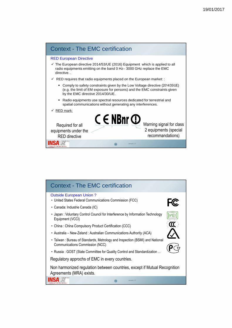
The European directive 2014/53/UE (2016) Equipment which is applied to all radio equipments emitting on the band 0 Hz– 3000 GHz replace the EMC directive. .
RED requires that radio equipments placed on the European market: :
Comply to safety constraints given by the Low Voltage directive (2014/35/UE) (e.g. the limit of EM exposure for persons) and the EMC constraints given by the EMC directive 2014/30/UE.
Radio equipments use spectral resources dedicated for terrestrial and spatial communications without generating any interferences.
RED mark:
Required for all equipments under the
RED directive
Warning signal for class 2 equipments (special
recommandations)
January 17
Context - The EMC certification
RED European Directive
70 January 17
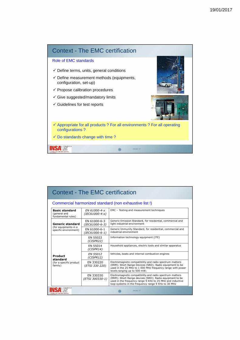
• United States Federal Communications Commission (FCC)
• Canada: Industrie Canada (IC)
• Japan : Voluntary Control Council for Interference by Information Technology Equipment (VCCI)
• China : China Compulsory Product Certification (CCC)
• Australia – New-Zeland : Australian Communications Authority (ACA)
• Taïwan : Bureau of Standards, Metrology and Inspection (BSMI) and National Communications Commission (NCC)
• Russia : GOST (State Committee for Quality Control and Standardization ...
Regulatory approchs of EMC in every countries.
Non harmonized regulation between countries, except if Mutual Recognition Agreements (MRA) exists.
Context - The EMC certification
Outside European Union ?
19/01/2017
71
Context - The EMC certification
Define terms, units, general conditions
Define measurement methods (equipments, configuration, set-up)
Propose calibration procedures
Give suggested/mandatory limits
Guidelines for test reports
Appropriate for all products ? For all environments ? For all operating configurations ?
Do standards change with time ?
January 17
Role of EMC standards
Commercial harmonized standard (non exhaustive list !)
Basic standard(general and fundamental rules)
EN 61000-4-x
(IEC61000-4-x)
EMC – Testing and measurement techniques
Generic standard(for equipments in a specific environment)
EN 61000-6-3 (IEC61000-6-3)
Generic Emission Standard, for residential, commercial and light industrial environment
EN 61000-6-1 (IEC61000-6-1)
Generic Immunity Standard, for residential, commercial and industrial environment
Product
standard(for a specific product family)
EN 55022(CISPR22)
Information technology equipment (ITE)
EN 55014(CISPR14)
Household appliances, electric tools and similar apparatus
EN 55012
(CISPR12)
Vehicles, boats and internal combustion engines
EN 330220 (ETSI 330 220)
Electromagnetic compatibility and radio spectrum matters (ERM); Short Range Devices (SRD); Radio equipment to be used in the 25 MHz to 1 000 MHz frequency range with power levels ranging up to 500 mW;
EN 330330(ETSI 300330-1)
Electromagnetic compatibility and radio spectrum matters (ERM); Short Range devices (SRD); Radio equipment to be used in the frequency range 9 KHz to 25 MHz and inductive loop systems in the frequency range 9 KHz to 30 MHz
72 January 17
Context - The EMC certification
19/01/2017
73
Automotive, military, aerospace and railway industries have developed their own EMC standards.
Applications Standard references
Automotive ISO 7637, ISO 11452, CISPR 25, SAE J1113
Aerospace DO-160, ED-14
Military MIL-STD-461D, MIL-STD-462D, MIL-STD-461E
Railway EN 50121
Commercial harmonized standard (non exhaustive list !)
January 17
Context - The EMC certification
74 January 17
Case study 1
Are the following product subject to the EMC European directive ?
Context - The EMC certification
WiFi dongle (ISM band)
Server motherboard
Passive antenna passive for RFID application
Wireless audio headset
19/01/2017
75 January 17
Case study 2
You want to place on the European
market a notebook.
Are you under the European EMC
directive 2014/30/UE ?
If yes, which EMC standard(s) should
you follow ? What tests should you
conduct for the EMC certification ?
Context - The EMC certification
76 January 17
Application of EN55022 : “Information technology equipment – Radio disturbance characteristics – Limits and methods of measurement” and EN55024 : « Information technology equipment – Immunity characteristics – Limits and methods of measurement » :
Any equipment dedicated to processing, storage, display, control of data and telecommunication messages, equipped with one or more ports, and supplied under less than 600 V.
Except equipments or modules dedicated only to radio emission or reception.
Case study 2
Context - The EMC certification
19/01/2017
77 January 17
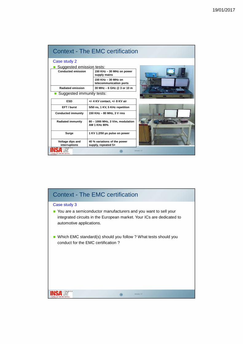
Case study 2 Suggested emission tests:
Suggested immunity tests:
Context - The EMC certification
Conducted emission 150 KHz – 30 MHz on power supply mains
150 KHz – 30 MHz on telecommunication ports
Radiated emission 30 MHz – 6 GHz @ 3 or 10 m
ESD +/- 4 KV contact, +/- 8 KV air
EFT / burst 5/50 ns, 1 KV, 5 KHz repetition
Conducted immunity 150 KHz – 80 MHz, 3 V rms
Radiated immunity 80 – 1000 MHz, 3 V/m, modulation AM 1 KHz 80%
Surge 1 KV 1.2/50 µs pulse on power
Voltage dips and interruptions
40 % variations of the power supply, repeated 5×
78
Case study 3
You are a semiconductor manufacturers and you want to sell your
integrated circuits in the European market. Your ICs are dedicated to
automotive applications.
Which EMC standard(s) should you follow ? What tests should you
conduct for the EMC certification ?
January 17
Context - The EMC certification
19/01/2017
79
Case study 3
If your integrated circuits can not operate by themselves, you don’t
need EMC certification.
However, your customers will certainly push you to guarantee the low
emission and susceptibility of your devices, require measurements,
models, support….
Examples of standards providing EMC measurement for ICs:
• IEC 61967: Integrated Circuits, Measurement of Electromagnetic Emissions, 150 kHz to 1 GHz
• IEC 62132: Integrated circuits - Measurement of electromagnetic immunity, 150 kHz to 1 GHz
• ISO11452: Road vehicles - Electrical disturbances by narrowband electromagnetic energy - Component test methods
• ISO 7637 or IEC61000-4-2/4/5 for ESD, pulse, surge testing.
January 17
Context - The EMC certification
80
Illustration of electromagnetic emission produced by electronic
devices
EMC measurements of components
January 17
19/01/2017
81
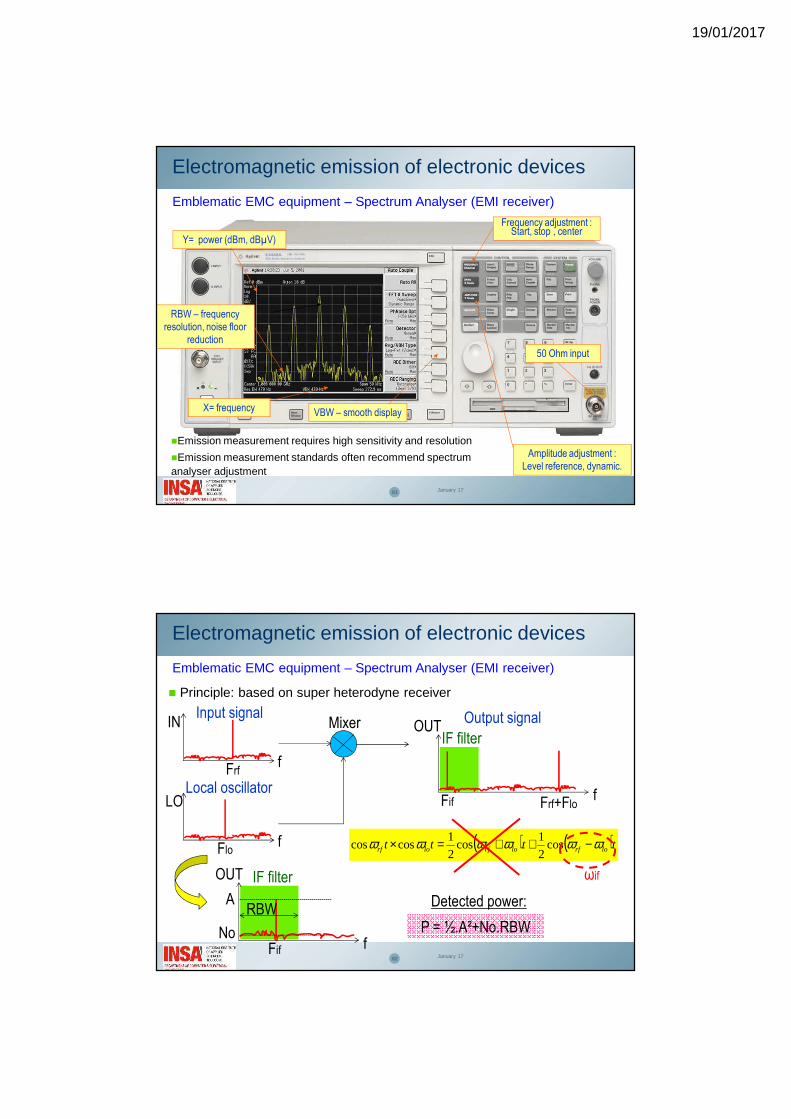
Electromagnetic emission of electronic devices
Emblematic EMC equipment – Spectrum Analyser (EMI receiver)
Frequency adjustment : Start, stop , center
Amplitude adjustment : Level reference, dynamic.
Emission measurement requires high sensitivity and resolution
Emission measurement standards often recommend spectrum analyser adjustment
RBW – frequency resolution, noise floor
reduction
VBW – smooth display
50 Ohm input
X= frequency
Y= power (dBm, dBµV)
January 17
82
Emblematic EMC equipment – Spectrum Analyser (EMI receiver)
Principle: based on super heterodyne receiver
( ) ( )tttt lorflorflorf ωωωωωω −++=× cos2
1cos
2
1coscos
IN
fFrf
LO
fFlo
Input signal
Local oscillator
Output signalOUT
fFif Frf+Flo
ωif
MixerIF filter
OUT
fFif
IF filter
A
No
RBWP = ½.A²+No.RBW
Detected power:
January 17
Electromagnetic emission of electronic devices
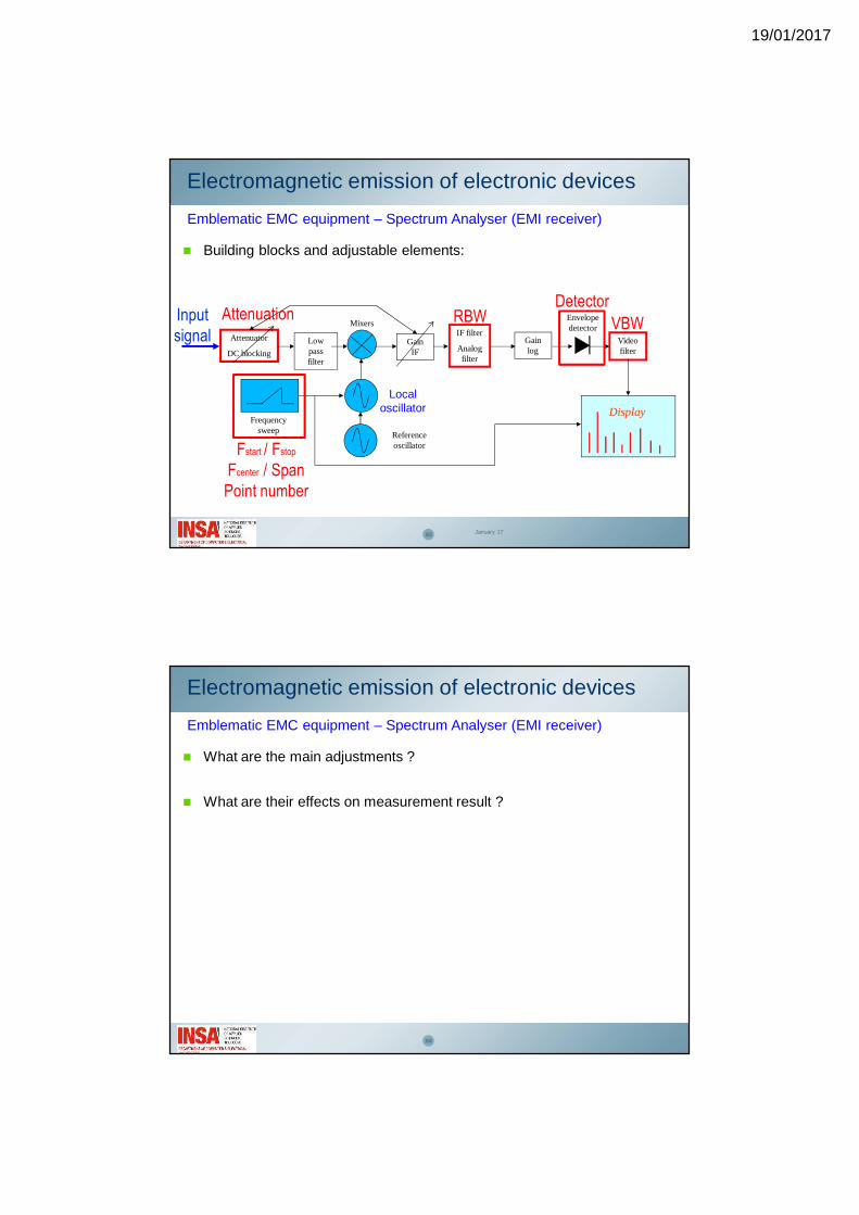
19/01/2017
83
Attenuator
DC blocking
Low pass filter
Gain IF
IF filter
Analog filter
Gain log
Video filter
Mixers
Local oscillator
Reference oscillator
Frequency sweep
Display
Envelope detector
Building blocks and adjustable elements:
Input signal
RBW VBW
DetectorAttenuation
Fstart / Fstop
Fcenter / SpanPoint number
Emblematic EMC equipment – Spectrum Analyser (EMI receiver)
January 17
Electromagnetic emission of electronic devices
84
What are the main adjustments ?
What are their effects on measurement result ?
Emblematic EMC equipment – Spectrum Analyser (EMI receiver)
Electromagnetic emission of electronic devices
19/01/2017
85
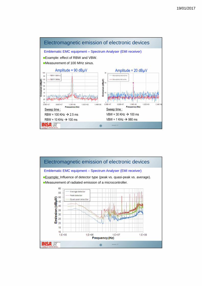
Example: effect of RBW and VBW.
Measurement of 100 MHz sinus.
Amplitude = 90 dBµV Amplitude = 20 dBµV
Sweep time :
RBW = 100 KHz 2.5 ms
RBW = 10 KHz 100 ms
Sweep time :
VBW = 30 KHz 100 ms
VBW = 1 KHz 980 ms
January 17
Emblematic EMC equipment – Spectrum Analyser (EMI receiver)
Electromagnetic emission of electronic devices
86
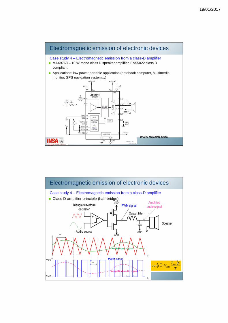
Example: Influence of detector type (peak vs. quasi-peak vs. average).
Measurement of radiated emission of a microcontroller.
January 17
Emblematic EMC equipment – Spectrum Analyser (EMI receiver)
Electromagnetic emission of electronic devices
19/01/2017
87
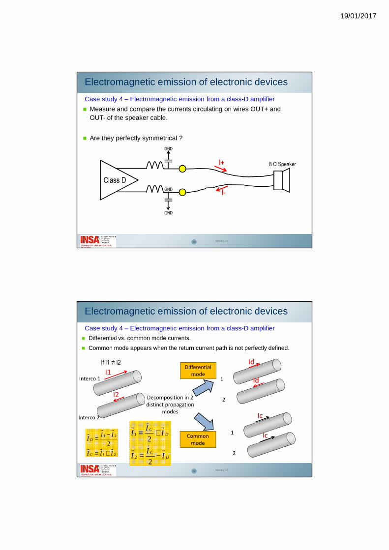
Case study 4 – Electromagnetic emission from a class-D amplifier
Electromagnetic emission of electronic devices
January 17
MAX9768 – 10 W mono class D speaker amplifier, EN55022 class B compliant.
Applications: low power portable application (notebook computer, Multimedia monitor, GPS navigation system…)
www.maxim.com
January 17
88
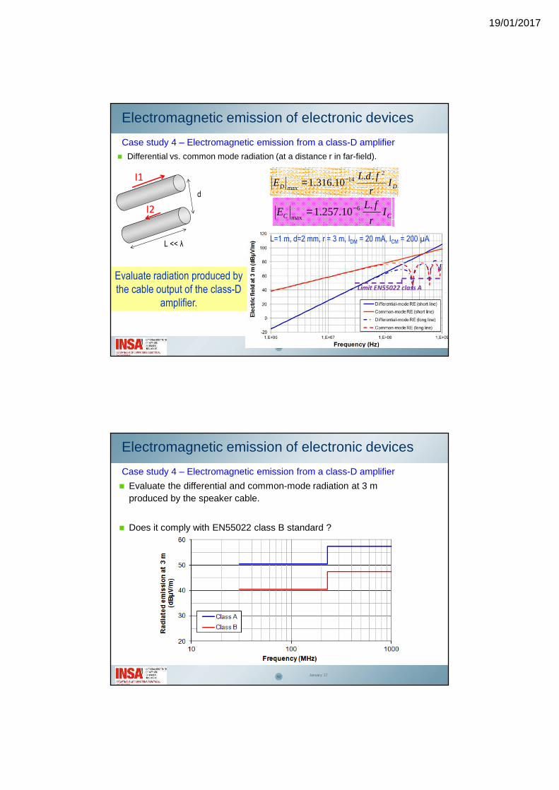
t
tGND
VDD
T
Tsw
PWM signal
Amplified audio signal
Audio input signal
January 17
Case study 4 – Electromagnetic emission from a class-D amplifier
Electromagnetic emission of electronic devices
Class D amplifier principle (half-bridge):
+
-
Triangle waveform oscillator
Audio sourceGND
VDD
GND
Output filter
PWM signalAmplified
audio signal
( ) ( )T
tTVtout SW
DD=
Speaker
19/01/2017
89 January 17
Case study 4 – Electromagnetic emission from a class-D amplifier
Electromagnetic emission of electronic devices
Measure and compare the currents circulating on wires OUT+ and OUT- of the speaker cable.
Are they perfectly symmetrical ?
Class D
GND
GND
GND
8 Ω SpeakerI+
I-
90
Case study 4 – Electromagnetic emission from a class-D amplifier
Electromagnetic emission of electronic devices
Differential vs. common mode currents.
Common mode appears when the return current path is not perfectly defined.
Interco 1
Interco 2
I1
I2
1
2
Id
Id
1
2
Ic
Ic
Decomposition in 2
distinct propagation
modes
Differential
mode
Common
mode
21
21
2
III
III
C
D
+=
−=
DC
DC
II
I
II
I
−=
+=
2
2
2
1
If I1 ≠ I2
January 17
19/01/2017
January 1791
Case study 4 – Electromagnetic emission from a class-D amplifier
Electromagnetic emission of electronic devices
Differential vs. common mode radiation (at a distance r in far-field).
I1
I2
d
L << λ
DD Ir
fdLE
214
max
..10.316.1 −=
CC Ir
fLE
.10.257.1 6
max
−=
Limit EN55022 class A
L=1 m, d=2 mm, r = 3 m, IDM = 20 mA, ICM = 200 µA
Evaluate radiation produced by the cable output of the class-D
amplifier.
92 January 17
Case study 4 – Electromagnetic emission from a class-D amplifier
Electromagnetic emission of electronic devices
Evaluate the differential and common-mode radiation at 3 m produced by the speaker cable.
Does it comply with EN55022 class B standard ?
19/01/2017
93 January 17
Case study 5 – Electromagnetic emission from a microcontroller
Osc
illa
tor
PLL
Digital Core
I/O
Vdd Dig
Vdd osc
Ext. Loads
Integrated
circuit
Icore(t)
Iosc(t)
Memory
Analog
IMem(t)
Vdd A
IA(t)
Vdd IO
IIO(t)
PCB lines
IIO(t)
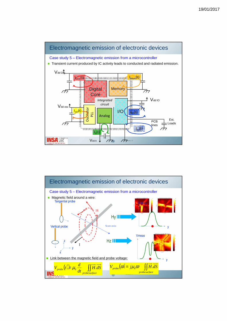
Transient current produced by IC activity leads to conducted and radiated emission.
Electromagnetic emission of electronic devices
January 17
Case study 5 – Electromagnetic emission from a microcontroller
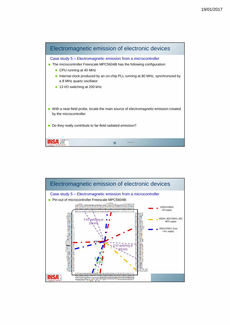
Magnetic field around a wire:
Electromagnetic emission of electronic devices
Hy
Hz
x
y
z
y
VmeasTangential probe
Vertical probe
y
Vmeas
I
H
Scan axis
( ) ∫∫=surfaceprobe
probe dSHdt
dtV .0µ
Link between the magnetic field and probe voltage:
( ) ∫∫=surfaceprobe
probe dSHjV .0ωµω
19/01/2017
95
Electromagnetic emission of electronic devices
January 17
Case study 5 – Electromagnetic emission from a microcontroller
The microcontroller Freescale MPC5604B has the following configuration:
CPU running at 40 MHz
Internal clock produced by an on-chip PLL running at 80 MHz, synchronized by a 8 MHz quartz oscillator
13 I/O switching at 200 kHz
With a near-field probe, locate the main source of electromagnetic emission created by the microcontroller.
Do they really contribute to far-field radiated emission?
96
Electromagnetic emission of electronic devices
January 17
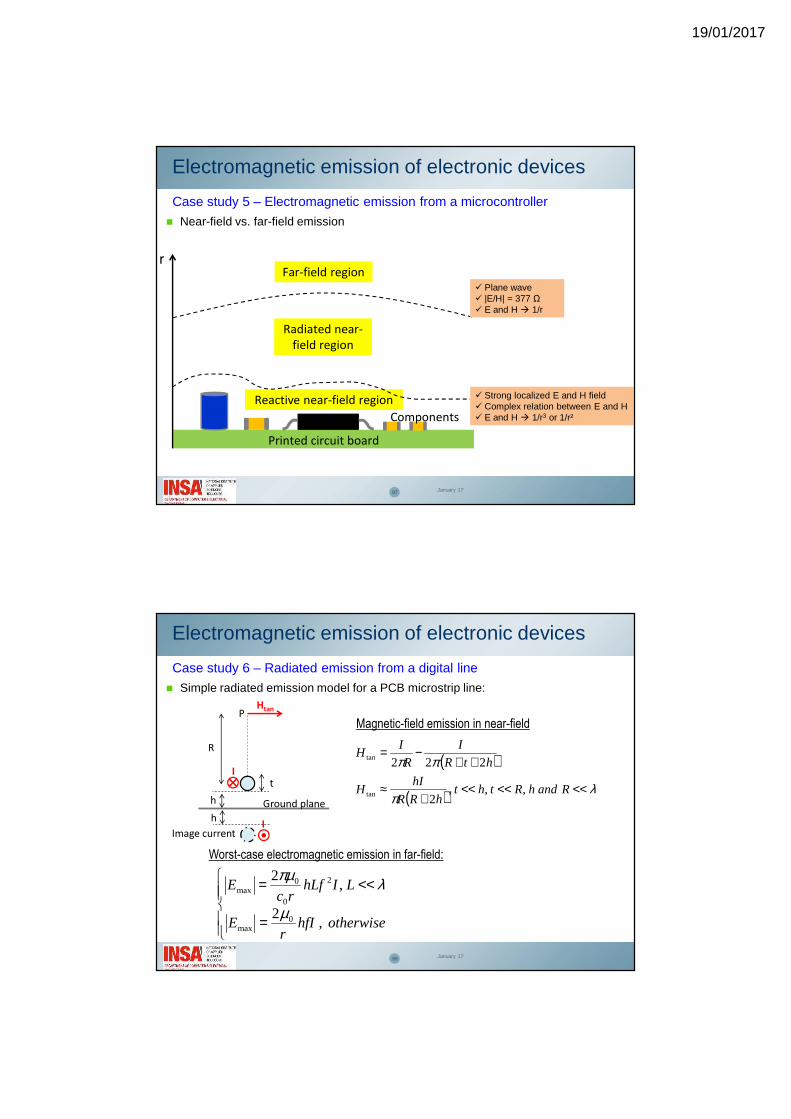
Case study 5 – Electromagnetic emission from a microcontroller
Pin-out of microcontroller Freescale MPC5604B:
5 I/O switching at 200 kHz
8 I/O switching at 200 kHz
VDDHV/VSSHV (I/O supply)
VDDHV_ADC/VSSHV_ADC (ADC supply)
External quartz
VDDLV/VSSLV (Core + PLL supply)
19/01/2017
97
Electromagnetic emission of electronic devices
January 17
Case study 5 – Electromagnetic emission from a microcontroller
Reactive near-field region
Printed circuit board
Components
rFar-field region
Radiated near-
field region
Strong localized E and H field Complex relation between E and H E and H 1/r3 or 1/r²
Plane wave |E/H| = 377 Ω E and H 1/r
Near-field vs. far-field emission
98
Electromagnetic emission of electronic devices
January 17
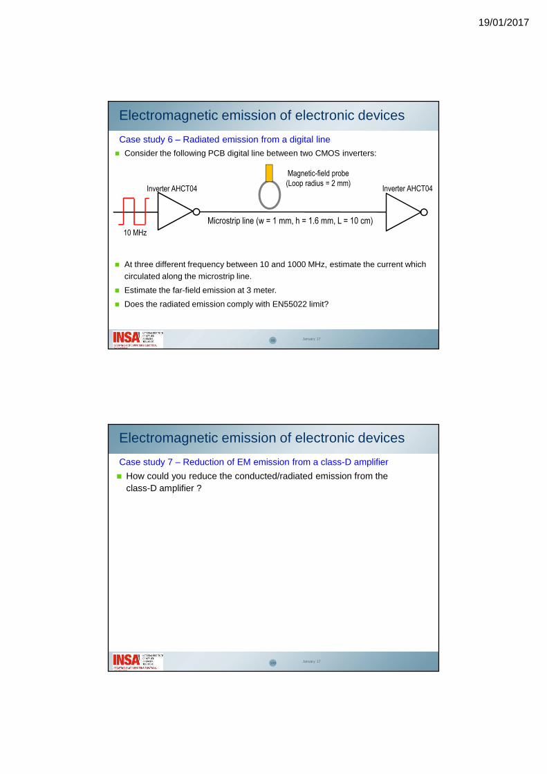
Case study 6 – Radiated emission from a digital line
Simple radiated emission model for a PCB microstrip line:
R
t
Htan
Ground plane
P
I
I
h
Image current
h
( )
( ) λπ
ππ
<<<<<<+
≈
++−=
RandhRththRR
hIH
htR
I
R
IH
,,,2
222
tan
tan
=
<<=
otherwisehfIr
E
LIhLfrc
E
,2
,2
0max
2
0
0max
µ
λπµ
Magnetic-field emission in near-field
Worst-case electromagnetic emission in far-field:
19/01/2017
99
Electromagnetic emission of electronic devices
January 17
Case study 6 – Radiated emission from a digital line
Consider the following PCB digital line between two CMOS inverters:
Microstrip line (w = 1 mm, h = 1.6 mm, L = 10 cm)
Inverter AHCT04 Inverter AHCT04
Magnetic-field probe (Loop radius = 2 mm)
At three different frequency between 10 and 1000 MHz, estimate the current which circulated along the microstrip line.
Estimate the far-field emission at 3 meter.
Does the radiated emission comply with EN55022 limit?
10 MHz
100 January 17
Case study 7 – Reduction of EM emission from a class-D amplifier
Electromagnetic emission of electronic devices
How could you reduce the conducted/radiated emission from the class-D amplifier ?
19/01/2017
101 January 17
Case study 7 – Reduction of EM emission by SSFM
Electromagnetic emission of electronic devices
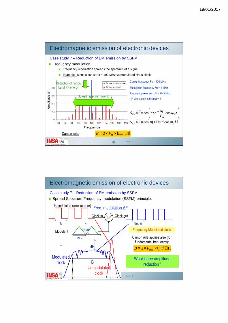
Frequency modulation : Frequency modulation spreads the spectrum of a signal
Example : sinus clock at Fc = 100 MHz vs modulated sinus clock:
( )
( ) ( )tmdttS
tF
dfttS
MCFM
MM
CFM
ωω
ωω
coscos
coscos
+=
+=
Spread spectrum over B
Reduction of narrow band RF energy
Carrier frequency Fc = 100 MHz
Modulation frequency FM = 1 MHz
Frequency excursion dF = +/- 5 MHz
Modulation index md = 5
Carson rule: ( )12 +××= mdFB M
102 January 17
Case study 7 – Reduction of EM emission by SSFM
Electromagnetic emission of electronic devices
Spread Spectrum Frequency modulation (SSFM) principle:
Clock in
Tc
Modulantt
Clock out
Tc+/-dt
Frequency Modulated clock
Freq. modulation ∆F
Unmodulated clock
Modulated clock
dP
B
TMod
+/- dt
Carson rule applies also (for fundamental frequency):
( )12 mod +××= mdFB
Unmodulated clock (carrier)
What is the amplitude reduction?
19/01/2017
103 January 17
Case study 7 – Reduction of EM emission by SSFM
Electromagnetic emission of electronic devices
Emission level improvement depends on:
Parameters of the modulation (md and Fm)
The modulant waveform (to make the spectrum as flat as possible)
Receiver bandwidth RBW
( )
≈RBW
BdBdP log10
P
f
unmodulated
SSFM
B
P
fB
RBW
dP
Measured SSFM signal
P
fB
RBWMeasured
SSFM signal
EMI receiver
104 January 17
Case study 7 – Reduction of EM emission by SSFM
Electromagnetic emission of electronic devices
Two output modulations:
Classic PWM mode
Filterless modulation mode
Three operating modes:
Fixed frequency (300 or 360 kHz)
SSFM (Fc = 300 kHz, df = +/- 7.5 kHz)
External clock (1 to 1.6 MHz)
Class-D amplifier MAX9768 internal features for emission management :

19/01/2017
105 January 17
Case study 7 – Reduction of EM emission by SSFM
Electromagnetic emission of electronic devices
Observe the effect of the internal SSFM on the fundamental frequency of the common-mode noise which propagates along the speaker cable. Use a narrow RBW.
Observe the effect of the internal SSFM on the spectrum of the common-mode noise which propagates along the speaker cable. Use a large RBW.
EN55022 recommends the following RBW:
• 9 kHz from 150 kHz to 30 MHz
• 120 kHz from 30 MHz to 1 GHz
Quantify the effect of the internal SSFM on the conducted emission spectrum?
106
Illustration of susceptibility to electromagnetic disturbances (RFI) of
electronic devices
EMC measurements of components
January 17
19/01/2017
107
Susceptibility of electronic devices to RFI
January 17
Effect of IC malfunction due to EM disturbance
Striking of berth by Coastal Inspiration, 20th dec 2011, Nanaimo, British Columbia, Canada.
A problem of an amplifier, due to EM disturbances, leads to a failure in speed reduction command.
108
Susceptibility of electronic devices to RFI
January 17
Case study 8 – Susceptibility of a bandgap reference voltage
LTC1798: 2.5 V micropower bandgap voltage reference
100 nF 100 nF
2.5 V +/- 4 mV2.7 V to 12 V LTC1798
RFI Effect on the output voltage ?
Couple an harmonic conducted disturbance to the input of the bandgap reference.
Observe the effect on the output voltage, for frequencies ranging from 1 to 100 MHz.
19/01/2017
109
Some EMC measurement tests
EMC measurements of components
January 17
110
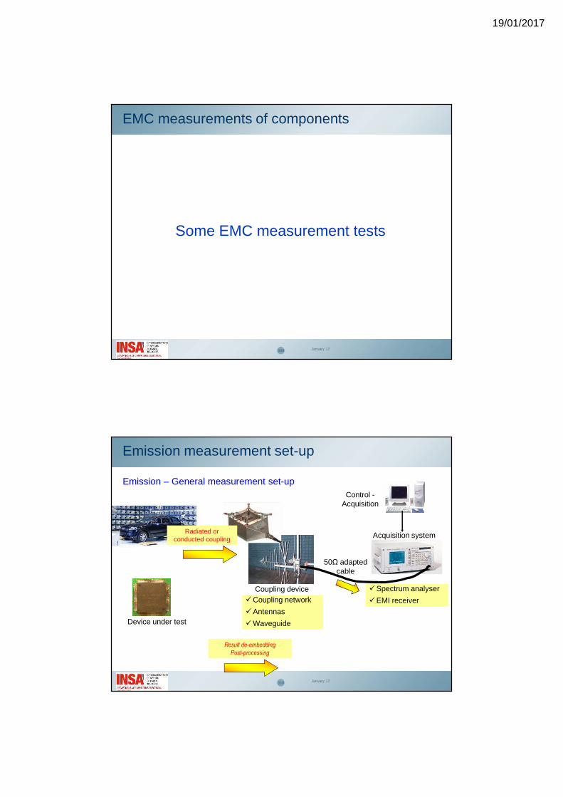
Emission measurement set-up
January 17
Device under test
Coupling deviceCoupling network
Antennas
Waveguide
Acquisition system
Spectrum analyser
EMI receiver
Emission – General measurement set-up
Radiated or conducted coupling
50Ω adapted cable
Control -Acquisition
Result de-embedding
Post-processing
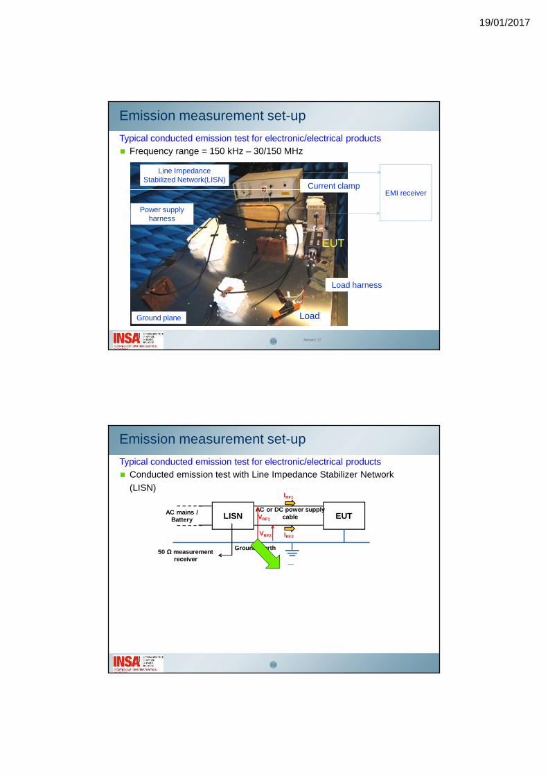
19/01/2017
111
Typical conducted emission test for electronic/electrical products
EUT
Load
Line Impedance Stabilized Network(LISN)
Current clamp
Power supply harness
Load harness
EMI receiver
Frequency range = 150 kHz – 30/150 MHz
Ground plane
January 17
Emission measurement set-up
112
Conducted emission test with Line Impedance Stabilizer Network
(LISN)
Emission measurement set-up
EUT
Ground, earth
AC mains /
Battery
AC or DC power supply
cable
Phase or ‘+’ conductor
Phase or ‘-’ conductor
VRF1
VRF2
IRF1
IRF2
EUT
Ground, earth
AC mains / Battery
AC or DC power supply cableVRF1
VRF2
IRF1
IRF2
LISN
50 Ω measurement receiver
Typical conducted emission test for electronic/electrical products
19/01/2017
113
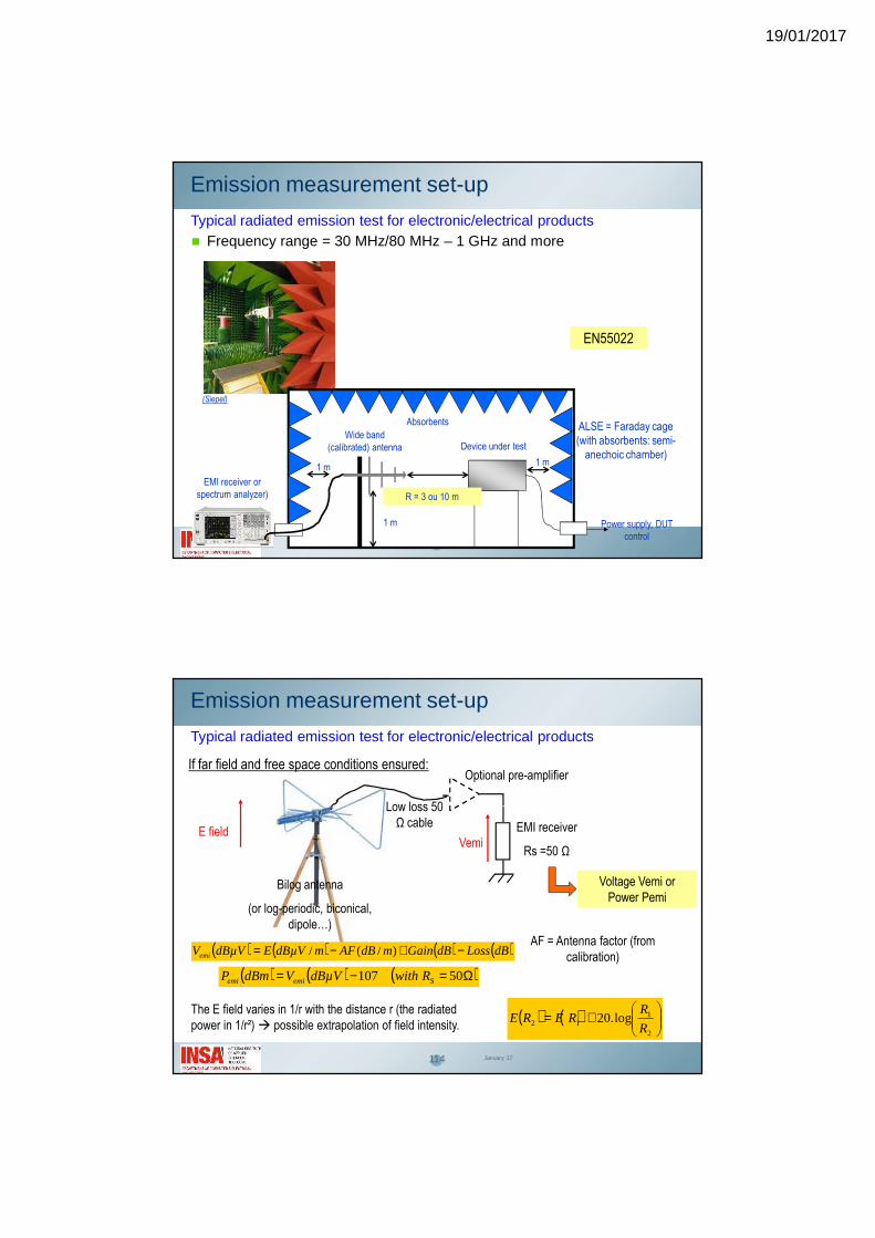
Device under testWide band
(calibrated) antenna
Power supply, DUT control
EMI receiver or spectrum analyzer)
Absorbents
R = 3 ou 10 m
1 m1 m
1 m
ALSE = Faraday cage (with absorbents: semi-
anechoic chamber)
(Siepel)
EN55022
Emission measurement set-up
Typical radiated emission test for electronic/electrical products Frequency range = 30 MHz/80 MHz – 1 GHz and more
E field EMI receiver
Rs =50 Ω
Optional pre-amplifier
Low loss 50 Ω cable
Bilog antenna
(or log-periodic, biconical, dipole…)
Vemi
If far field and free space conditions ensured:
( ) ( ) ( ) ( )dBLossdBGainmdBAFmdBµVEdBµVVemi −+−= )/(/AF = Antenna factor (from
calibration)
The E field varies in 1/r with the distance r (the radiated power in 1/r²) possible extrapolation of field intensity.
114 January 17
Voltage Vemi or Power Pemi
( ) ( ) ( )Ω=−= 50107 Semiemi RwithdBµVVdBmP
Emission measurement set-up
Typical radiated emission test for electronic/electrical products
( ) ( )
+=
2
112 log.20
R
RRERE
19/01/2017
115
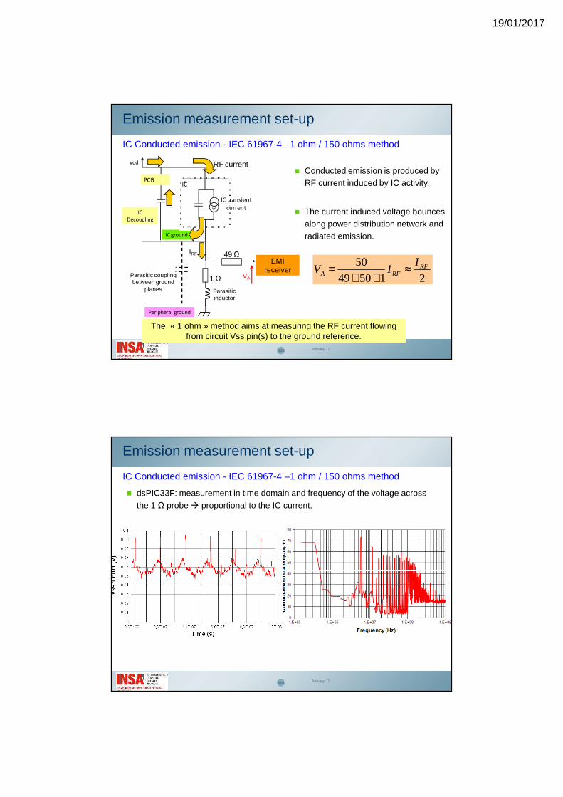
IC Conducted emission - IEC 61967-4 –1 ohm / 150 ohms method
January 17
Conducted emission is produced by RF current induced by IC activity.
The current induced voltage bounces along power distribution network and radiated emission.
The « 1 ohm » method aims at measuring the RF current flowing from circuit Vss pin(s) to the ground reference.
215049
50 RFRFA
IIV ≈
++=
IC ground
ICPCB
IC
Decoupling
RF currentVdd
Peripheral ground
EMI receiver
1 Ω
49 ΩIRF
VA
Parasitic inductor
Parasitic coupling between ground
planes
IC transient
current
Emission measurement set-up
116
dsPIC33F: measurement in time domain and frequency of the voltage across the 1 Ω probe proportional to the IC current.
January 17
Emission measurement set-up
IC Conducted emission - IEC 61967-4 –1 ohm / 150 ohms method
19/01/2017
117
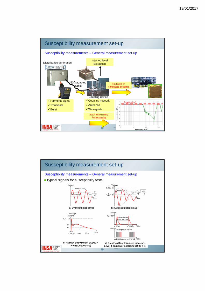
Susceptibility measurements – General measurement set-up
January 17
Coupling deviceCoupling network
Antennas
Waveguide
Radiated or conducted coupling
Disturbance generation
Harmonic signal
Transients
Burst
50Ω adapted cable
Injected level Extraction
Result de-embedding
Port-processing
0
5
10
15
20
25
30
35
1 10 100 1000
Fo
rwa
rd p
ow
er
(dB
m)
Frequency (MHz)
Power limit
Device under test
Susceptibility measurement set-up
118
Time
Voltage
RMS voltage 21
2
2mVV A
RMS +=
a) Unmodulated sinus
Amplitude VAAmplitude VA
( )mVA +1
Time
Voltage
( )mVA −1
b) AM modulated sinus
c) Human Body Model ESD at 4 KV (IEC61000-4-2)
d) Electrical fast transient in burst –Level 4 on power port (IEC 61000-4-4)
Time
Discharge current
Time
Voltage
AI P 15=
nstr 8.0= ns30
A8
A4
ns60
Time
VoltageBurst period 300 ms
Burst duration 0.75 or 15 ms
KVVP 4=Repetition rate 5 or 100 KHz
nstr 5= nstr 50=
2A
RMS
VV =
Typical signals for susceptibility tests:
Susceptibility measurements – General measurement set-up
Susceptibility measurement set-up
January 17
19/01/2017
119
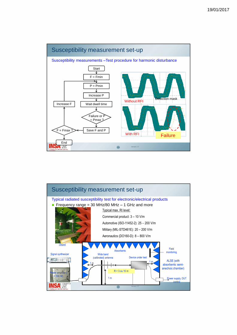
Susceptibility measurements –Test procedure for harmonic disturbance
Start
F = Fmin
P = Pmin
Increase P
Wait dwell time
Failure or P = Pmax ?
Save F and PF = Fmax ?
End
Increase FWithout RFI
With RFI Failure
Detection mask
January 17
Susceptibility measurement set-up
120
Device under testWide band
(calibrated) antenna
Power supply, DUT control
Absorbents
R = 3 ou 10 m
1 m1 m
1 m
ALSE (with absorbents: semi-
anechoic chamber)
(Siepel)
Power amplifier ( > 100 W)
Signal synthesizer
Field monitoring
Typical max. RI level:
Commercial product: 3 – 10 V/m
Automotive (ISO-11452-2): 25 – 200 V/m
Military (MIL-STD461E): 20 – 200 V/m
Aeronautics (DO160-D): 8 – 800 V/m
January 17
Susceptibility measurement set-up
Typical radiated susceptibility test for electronic/electrical products Frequency range = 30 MHz/80 MHz – 1 GHz and more
19/01/2017
121
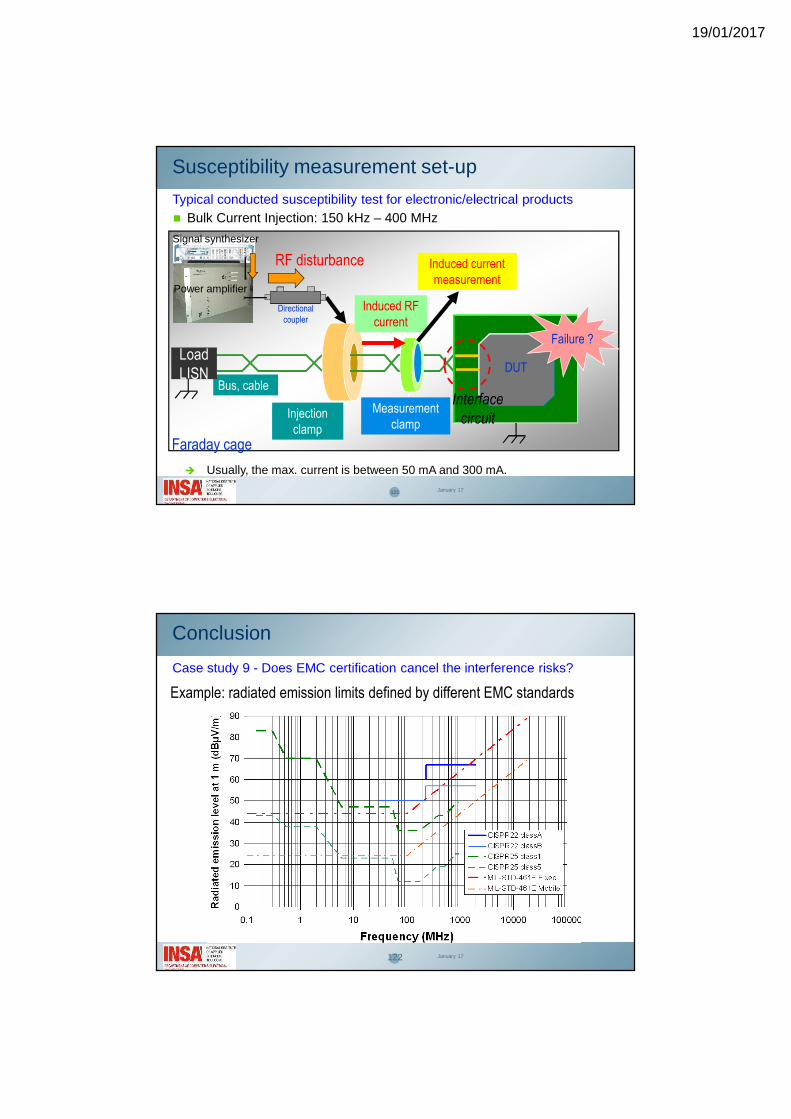
Injection clamp
Induced RF current
Bus, cable
Microcontroler
DUT
Failure ?
Measurement clamp
Directional coupler
Signal synthesizer
RF disturbance
LoadLISN
Induced current measurement
Interface
circuit
Faraday cage
Usually, the max. current is between 50 mA and 300 mA.
Power amplifier
January 17
Susceptibility measurement set-up
Typical conducted susceptibility test for electronic/electrical products Bulk Current Injection: 150 kHz – 400 MHz
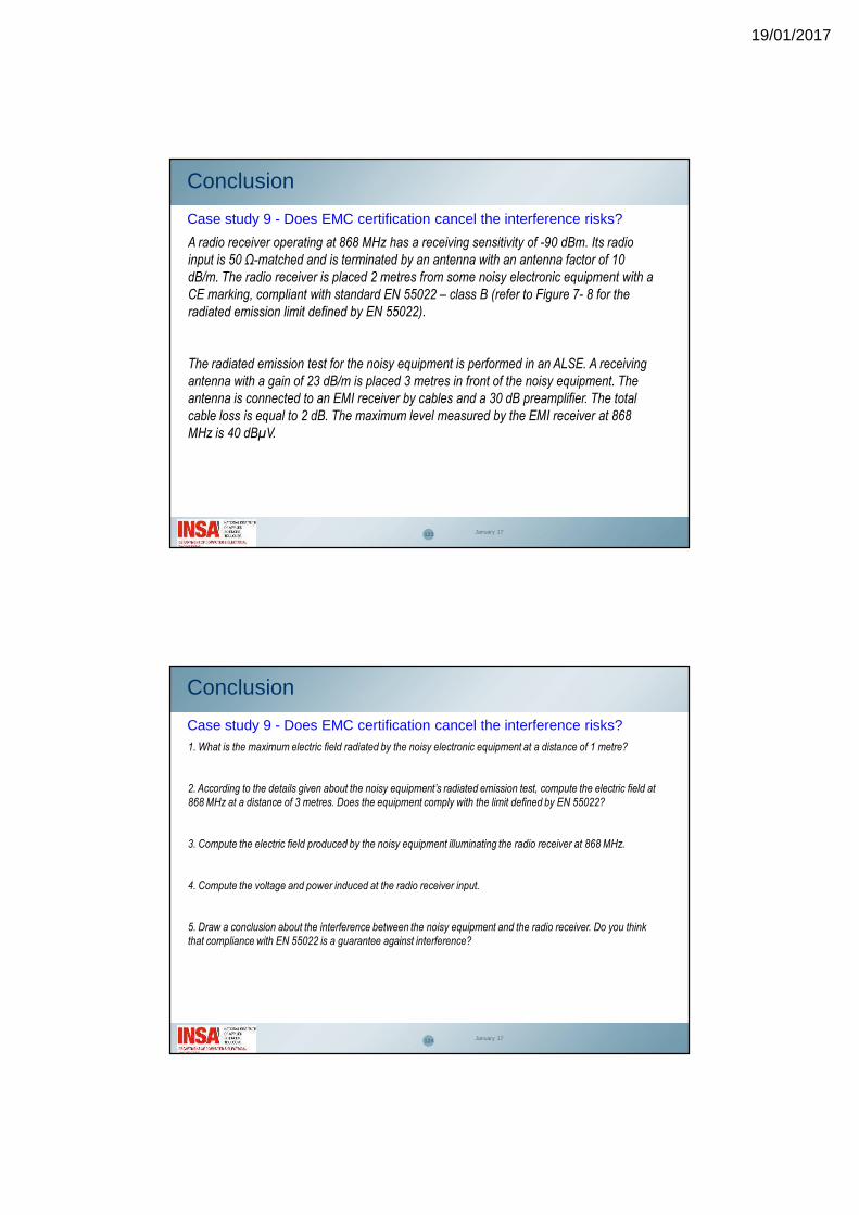
Case study 9 - Does EMC certification cancel the interference risks?
Example: radiated emission limits defined by different EMC standards
122 January 17
Conclusion
19/01/2017
123 January 17
A radio receiver operating at 868 MHz has a receiving sensitivity of -90 dBm. Its radio
input is 50 Ω-matched and is terminated by an antenna with an antenna factor of 10
dB/m. The radio receiver is placed 2 metres from some noisy electronic equipment with a
CE marking, compliant with standard EN 55022 – class B (refer to Figure 7- 8 for the
radiated emission limit defined by EN 55022).
The radiated emission test for the noisy equipment is performed in an ALSE. A receiving
antenna with a gain of 23 dB/m is placed 3 metres in front of the noisy equipment. The
antenna is connected to an EMI receiver by cables and a 30 dB preamplifier. The total
cable loss is equal to 2 dB. The maximum level measured by the EMI receiver at 868
MHz is 40 dBµV.
Conclusion
Case study 9 - Does EMC certification cancel the interference risks?
124 January 17
1. What is the maximum electric field radiated by the noisy electronic equipment at a distance of 1 metre?
2. According to the details given about the noisy equipment’s radiated emission test, compute the electric field at
868 MHz at a distance of 3 metres. Does the equipment comply with the limit defined by EN 55022?
3. Compute the electric field produced by the noisy equipment illuminating the radio receiver at 868 MHz.
4. Compute the voltage and power induced at the radio receiver input.
5. Draw a conclusion about the interference between the noisy equipment and the radio receiver. Do you think
that compliance with EN 55022 is a guarantee against interference?
Conclusion
Case study 9 - Does EMC certification cancel the interference risks?
19/01/2017
125 January 17
Conclusion
Evaluation of emission/susceptibility problems of circuits
Circuit Emission issues
Susceptibilityissues
Justification
Driver chip for a TFT LCD monitor
LDO linear voltage regulator
Boost converter
IEEE 802.15.4 Zigbee transceiverchip
FPGA supporting numerous high speed interfaces
LIN bus driver for automotive application


![INTEGRATED DISEASE SURVEILLANCE PROGRAMME (IDSP) [Compatibility Mode].pdf · Integrated Disease Surveillance Programme ... – Form P (Probable Cases): Doctors ... S,P,L forms & EWS](https://static.fdocuments.in/doc/165x107/5b1d22937f8b9a16788c006b/integrated-disease-surveillance-programme-idsp-compatibility-modepdf-integrated.jpg)


![Integrated food security programme south gonder (gtz) [compatibility mode]](https://static.fdocuments.in/doc/165x107/5402bfb78d7f72f24a8b4612/integrated-food-security-programme-south-gonder-gtz-compatibility-mode.jpg)


![Integrated quality management [compatibility mode]](https://static.fdocuments.in/doc/165x107/546ecd96b4af9fa5268b4805/integrated-quality-management-compatibility-mode.jpg)
