Electromagnetic Compatibility of Integrated Circuits (EMC...
105
1 April 27 th , 2009 Alexandre Boyer [email protected] INSA de Toulouse, France Electromagnetic Compatibility of Integrated Electromagnetic Compatibility of Integrated Circuits (EMC of ICs) Circuits (EMC of ICs)
Transcript of Electromagnetic Compatibility of Integrated Circuits (EMC...

1
April 27th, 2009
Alexandre Boyer
INSA de Toulouse, France
Electromagnetic Compatibility of Integrated Electromagnetic Compatibility of Integrated Circuits (EMC of ICs)Circuits (EMC of ICs)

2
OUTLINE
AGENDA
9h - 12h: EMC of ICs – part I (Course)
14h - 17h: EMC of ICs – part II (Lab activity)
OBJECTIVES
At the end of the course, the auditor will be able to understand the origins of electromagnetic compatibility (EMC) issues at integrated circuits level, the basic knowledge to face with EMC issues, and become familiar with the most common circuit-level EMC design guidelines.
PRE REQUISITES
Basic knowledge in electrical circuits, CMOS technology, electromagnetism, electrical simulation (SPICE).
3
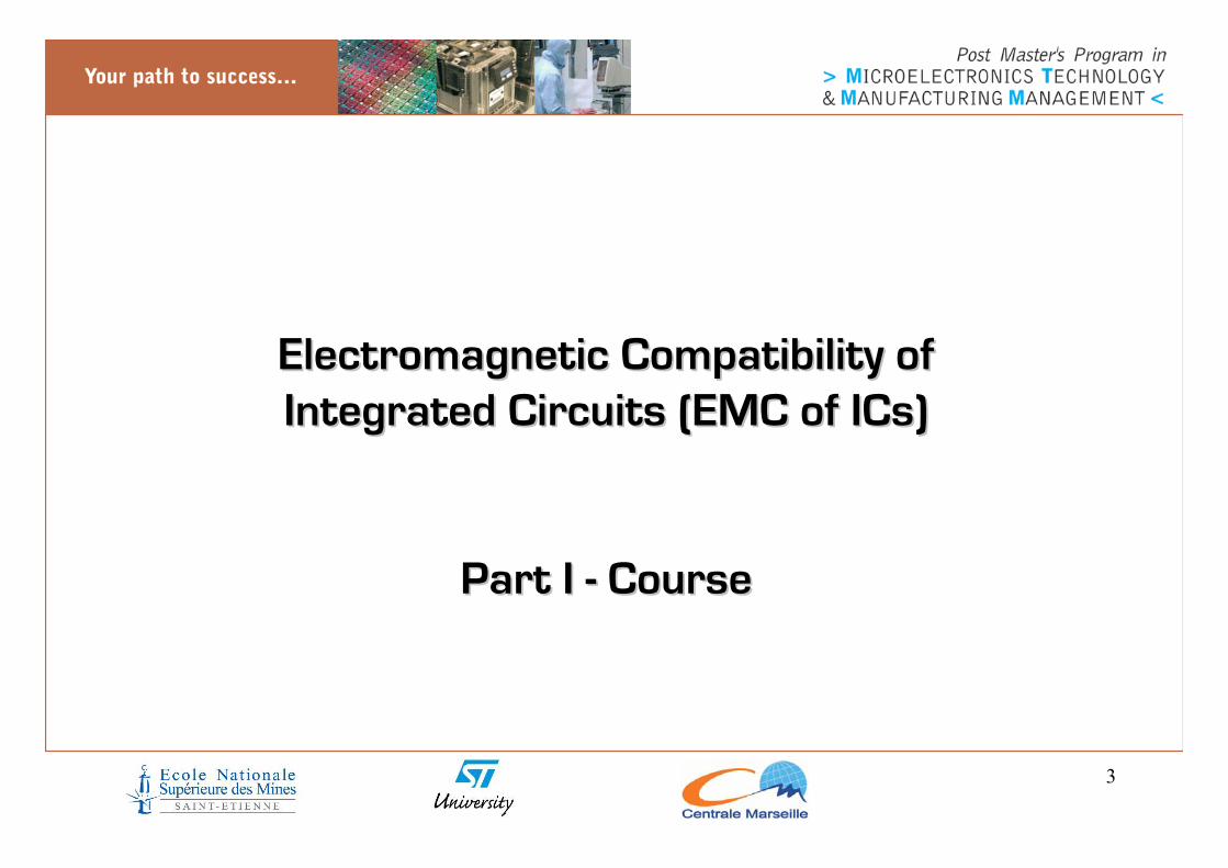
Electromagnetic Compatibility of Electromagnetic Compatibility of Integrated Circuits (EMC of ICs)Integrated Circuits (EMC of ICs)
Part I Part I -- CourseCourse

4
OUTLINE CONTENT
Introduction
EMC Basics concepts
Emission/Susceptibility Origin
Measurement methods
EMC Guidelines
Conclusion

5
1. Introduction
6
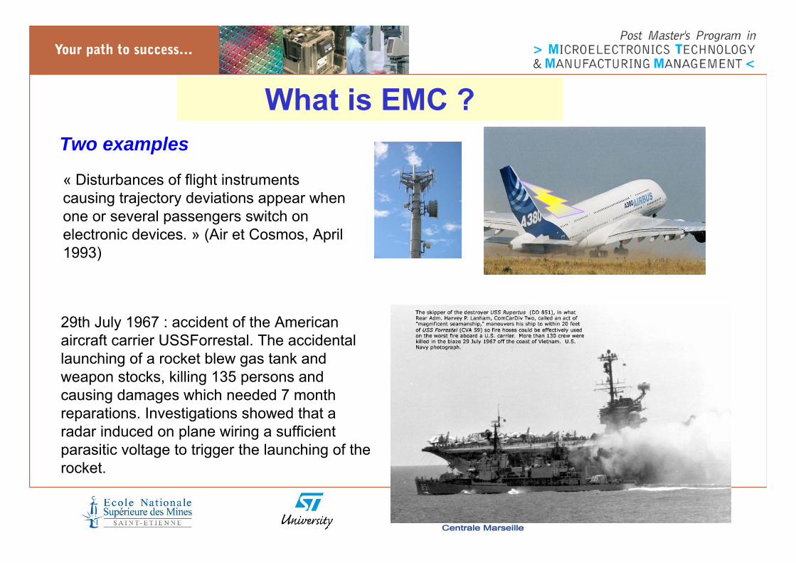
What is EMC ?
« Disturbances of flight instruments causing trajectory deviations appear when one or several passengers switch on electronic devices. » (Air et Cosmos, April 1993)
29th July 1967 : accident of the American aircraft carrier USSForrestal. The accidental launching of a rocket blew gas tank and weapon stocks, killing 135 persons and causing damages which needed 7 month reparations. Investigations showed that a radar induced on plane wiring a sufficient parasitic voltage to trigger the launching of the rocket.
Two examples
7
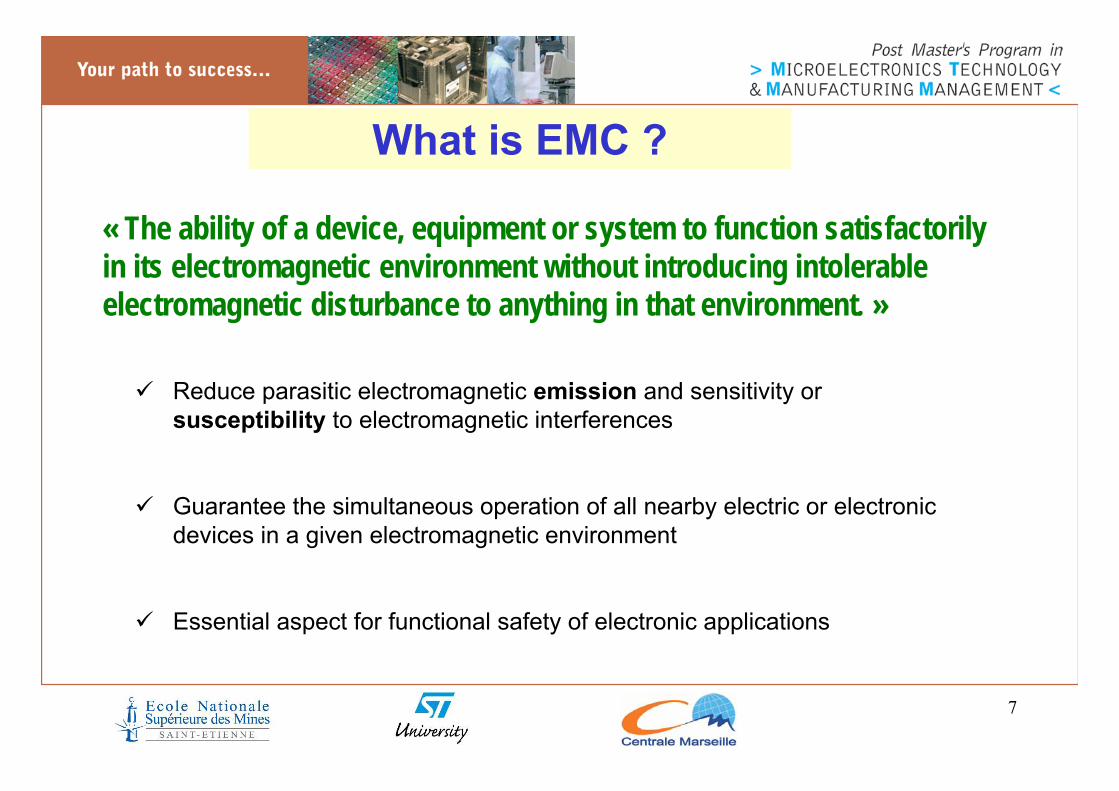
What is EMC ?
« The ability of a device, equipment or system to function satisfactorily in its electromagnetic environment without introducing intolerable electromagnetic disturbance to anything in that environment. »
Reduce parasitic electromagnetic emission and sensitivity or susceptibility to electromagnetic interferences
Guarantee the simultaneous operation of all nearby electric or electronic devices in a given electromagnetic environment
Essential aspect for functional safety of electronic applications

8
What is EMC ?EMC certification
Electronic devices dedicated to critical applications in term of safety and robustness must respond to EMC specifications.
They define maximum levels and methods to characterize emission and susceptibility of an equipment are defined by standards
EMC standards for automotive, aerospace, military, transport, medical, telecommunication applications, but also for commercial products
• European EMC directive 89/336/EEC about electronic products EMC requirements
• For automotive applications : ISO 7637, ISO 11452, CISPR 25, SAE J1113
• For military applications : MIL-STD-461D, MIL-STD-462D
• For aerospace applications : DO-160
• For integrated circuits : IEC 61963, IEC 62132
CE mark

9
Technology trends
2000 2005 2010 2015
10nm
100nm
1μm
Technology (log scale)
Year
0.13μm90nm 45nm
32nm
Technology trend high performance microprocessors
22nm
20201nm
7nm18nm
9nm
0.18μm 0.13µm
65nm
Technology trend cost-performance
microcontrollers0.25μm0.35μm
90nm
45nm32nm
5-years gap22nm
Year
Consequences on electronic systems safety,
reliability, … and EMC

10
EMC of ICs
• Until mid 90’s, IC designers had no consideration about EMC problems in their design. EMC was only handled at system and PCB levels
• Many EMC problems originate from ICs (3rd origin of IC redesign !), as it is the source of noise emission and sensitivity
• With technology trends (increased clock speed, chip complexity and reduced voltage), ICs are more emissive and sensitive to noise
• Semiconductor manufacturers are faced with increasing customer expectations for designing low emission and highly immune ICs
EMC must be handled at IC level
Why EMC of ICs

11
EMC of ICsDesign issues
EMC problems handled at the end of design cycle
DESIGN
Architectural Design
Design EntryDesign Architect
FABRICATION
Version n°
EMC Measurements
GONO GO
+ 6 months
+ $$$$$$$$
Compliance ?
Version n°

12
DESIGN
Architectural Design
Design EntryDesign Architect
FABRICATION
EMC compliant
EMC SimulationsCompliance ?
GO
NO GO
EMC validated before fabricationDesign Guidelines
Tools
Training
EMC problems handled at the end of design cycle
EMC of ICsDesign issues
13
2. EMC Basic Concepts

14
P=H2 x 377 (watts/m2) far field conditions
P=I2 x R (watts)
Z=E/HZ=V/I
Characteristic impedance Z0 (Ohm)Impedance Z (Ohm)
Magnetic field H (A/m)Current I (Amp)
Electric Field E (V/m)Voltage V (Volt)
Electromagnetic domainElectrical domain
The “EMC” way of thinking
EMC environment

15
Wide dynamic range of signals in EMC → use of dB (decibel)
0.1
10
1
100
0.01
Volt dBV
0.001
0.001
0.1
0.01
1
0.0001
MilliVolt dBµV
0.00001
Extensive use of dB for voltage units
For example dBV, dBA :
( )( )AdBAVdBV
log20log20
×=×=
Extensive use of dBµV
( ) 120log201
log20 +×=⎟⎟⎠
⎞⎜⎜⎝
⎛×= V
µVVVdBµV
0
20
40
-20
-40
-60
0
20
40
-20
-40
60
Specific Units
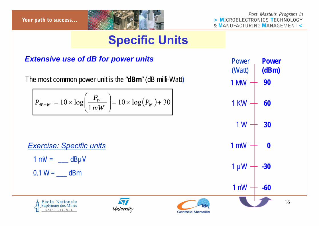
16
Specific UnitsExtensive use of dB for power units
The most common power unit is the “dBm” (dB milli-Watt)
1 mV = ___ dBµV
0.1 W = ___ dBm
Exercise: Specific units
( ) 30log101
log10 +×=⎟⎟⎠
⎞⎜⎜⎝
⎛×= W
WdBmW P
mWPP
1 W
1 MW
1 KW
Power(Watt)
1 mW
Power(dBm)
1 µW
1 nW
30
90
60
0
-30
-60

17
Emission and susceptibility level units
30K 300K 3M 30M40
50
60
70
80
dBµV
Conducted emission level (CISPR25)
Class 4
Class 5
1M 100M 1G10
20
30
40
50
dBµV/m
Radiated emission level (CISPR25)
Class 5
10M
CISPR 25 : “Radio disturbance characteristics for the protection of receivers used on board vehicles, boats, and on devices – Limits and methods of measurement”
Specific Units

18
Fourier Transform
Time domain measurement
Volt
Time
Frequency measurementFourier transform
Freq (Log)
dB
Invert Fourier transform
Fourier transform: principle
Spectrum analyserOscilloscope

19
Fourier TransformWhy Frequency domain is so important for EMC?
FFT
User’s specification
Time domain Frequency domain
Low level harmonics contribution
Only high level harmonics contribution appears
Contribution of each harmonic appears

20
Fourier transform - Example
50 % duty cycle trapezoidal signal
Period T = 100 ns, Tr = Tf = 2 ns
FFT
Fourier Transform
Fast evaluation of signal bandwidth

21
Two main conceptsEmission of EM wavesSusceptibility to EM waves
Personal entrainments
Safety systems
interferences
Hardware faultSoftware failureFunction Loss
Components
Printed circuit boards
EquipmentsSystem
Noise

22
Victim
Aggressor
Coupling method:
• Conducted
• Radiated
Basic EMC problem
Solving EMC issues consists in acting on these 3 different elements.
Electromagnetic emission
Electromagnetic induced failure

23
Emission spectrum
Specification for an IC emission
Parasitic emission (dBµV)
-10
0
1020
30
405060
70
80
1 10 100 1000Frequency (MHz)
Measured emission
EMC compatible
Aggressor IC
Radiated emission
Sufficient margin

24
Susceptibility threshold
Immunity level (dBmA)
-40
-30
-20-10
0
10
2030
40
50
1 10 100 1000
Specification for board immunityCurrent injection limit
Measured immunity
A very low energy produces a fault
Frequency (MHz)
Victim IC

25
Notion of margin
0 dB 1 yearConsumer
20 dB10 yearsAutomotive
40 dB30 yearsAeronautics
MarginLifetimeDomain
Parasitic emission (dBµV)
Component/PCB/System Ageing
Nominal Level
Design Objective
Process dispersion
Measurement error/dispersion
Environment
Safety margin
To ensure the electromagnetic compatibility, emission or susceptibility levels have to be lower than a nominal target …
…But it is not sufficient to cancel all risks of failures !
Margin are required to compensate unpredictable variations and reduce failure appearance probability.
Margin depends on the safety level required in an application domain:
26
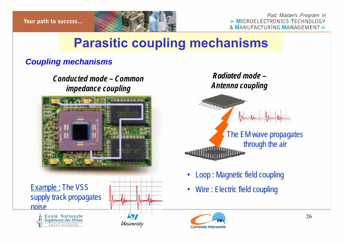
Parasitic coupling mechanisms
Radiated mode –Antenna coupling
Example : The VSS supply track propagates noise
The EM wave propagates through the air
Coupling mechanisms
Conducted mode – Common impedance coupling
• Loop : Magnetic field coupling
• Wire : Electric field coupling

27
Parasitic coupling mechanismsCrosstalk
Parasitic coupling between nearby conductors.
Near field coupling ≠ radiated coupling
Capacitive crosstalk Inductive crosstalk
dielectricground
C C
C12
h
t
wd
dielectricground
L12
h
t
wddtdVCI =
dtdILV =

28
ImpedanceR,L,C vs. frequency
Impedance profile of:
•50 ohms resistor
•100pF capacitor
•10nH inductor
•a real 100 pF SMD capacitor
Z = constant
Z÷10 at each decade
Z×10 at each decade

29
Ceramic capacitor
Carbon resistor
Inductor
ImpedancePassive components – Real model
Understand EMC issues requires the knowledge of electronic device parasitics

30
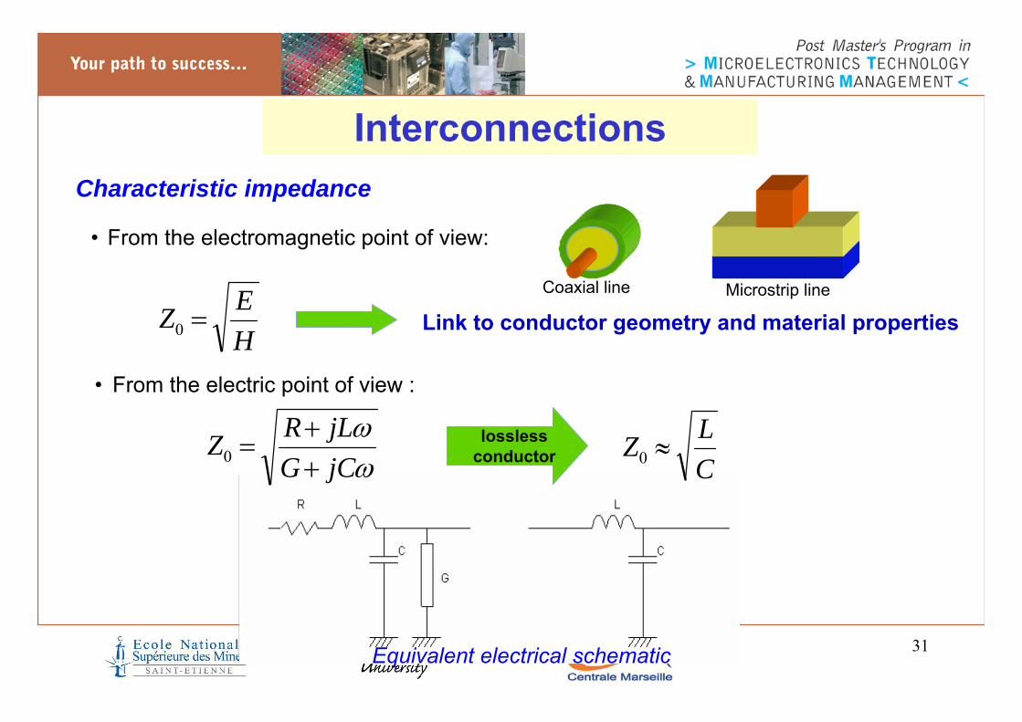
Interconnections
2a
l
I
acdc RRR +=
2alRdc σπ
= δπσ alRac 2
=
⎟⎟⎠
⎞⎜⎜⎝
⎛−⎟⎠⎞
⎜⎝⎛×= 12ln
2 allL o
πμ Quasi static approximation : If l < λ/20,
interconnections are considered as electrically small.
PCB
Package
Bonding wires
Parasitic resistance
Parasitic inductance
Interconnect parasitics
Interconnections are not equipotentials !
31
Interconnections
Coaxial line Microstrip line
• From the electromagnetic point of view:
HEZ =0 Link to conductor geometry and material properties
ωω
jCGjLRZ
++
=0 CLZ ≈0
losslessconductor
• From the electric point of view :
Equivalent electrical schematic
Characteristic impedance

32
InterconnectionsImpedance matching
Adapted: the line is transparentNot adapted: the signal suffers from distortions: ringing, insertion losses
time
Voltage
time
Voltage
Essential for signal integrity and power transfer

33
InterconnectionsCharacteristic impedance Small conductor Large conductor
What is the optimum characteristic impedance for a coaxial cable ?
• Maximum power : Z0 = 32 Ω• Minimum loss: Z0 = 77 Ω
xLow Impedance
xSmall inductance
xSmall capacitance
xxLow loss
Xweight
XBending
XPower handling
Large conductor
Small conductor
Or ?
Ideal values:
• EMC cable (compromise between power and loss) : Z0 = 50 Ω
• TV cable (minimize Loss): Z0 = 75 Ω
Cable examples:

34
50 Ω adapted equipments
Gtem
Tem cell
Spectrum analyzer
Waveform generator
Amplifier
EMC equipments
35
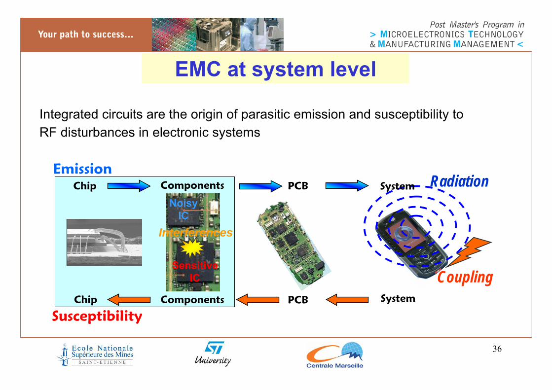
3. Origin of Emission and Susceptibility of ICs
36
Susceptibility
Chip
Chip
EmissionPCB
PCB System
Components
Components
System
Integrated circuits are the origin of parasitic emission and susceptibility to RF disturbances in electronic systems
Noisy IC
Sensitive IC
Interferences
Radiation
Coupling
EMC at system level

37
Source of Electromagnetic Interferences Natural disturbances
(cosmic rays, thunder)Radio communications,
wireless, radars,…
ElectricalOverstress
Inductive loads, motors
IC activity
IC

38
VDD
VSS
Output capa
Vin
Basic mechanisms for CMOS circuit current: CMOS inverter example
IDD (0.1mA)
ISS (0.1mA)
IDD (0.1mA)
ISS (0.1mA)
VOUT
Switching current
Voltage Time
Time
Origin of parasitic emission
Main noise sources comes from AC current sources:- Clock-driven blocks, synchronized logic- I/O switching

39
Origin of parasitic emissionParasitic emission is linked to voltage drops... But only current peaks can not explained completely electromagnetic emission.
Inductance are responsible of the conversion of current peak to voltage drops.
Current peaks and voltage drops generate the conducted emission and then the radiated emission.
Vss
Vdd
50ps
i(t)
Time
Switching gatesInternal
switching noise
Vdd
Vss
i(t)
Voltage dropstiLV
ΔΔ
=Δ
i(t)Radiated Emission

40
Stronger di/dtStronger di/dt
Increase parasiticnoise
Increase parasiticnoise
Time
New process
VoltOld process
Why technology scale down makes things worse ?
• Current level keeps almost constant but:
• Faster current switching
• Current level keeps almost constant but:
• Faster current switching
Time
Current
di/dt
New processOld process
Origin of parasitic emission

41
Example: evaluation of switching current in an IC
• 0.1 mA / Gate in 100ps• 1 Billion gates (32 Bit Micro) =>• 10% switching activity => • Spreading of current peak (non synchronous switching) =>
Ampere
time
Vdd
Vss
i(t)Current / gate
Ampere
time
Current / Ic
Origin of parasitic emission

42
Example: evaluation of supply voltage bounce
L=0.6nH/mm
L=1nH/mmLead = 10 mm
1 A en 1 ns Evaluate noise amplitude :
VDD
VSS
Lead = 10 mm
Chip
Origin of parasitic emission

43
Origin of parasitic emissionOverview of influent parameters on parasitic emission
circuit
i(t)IC Internal
interconnexions
IC activity
PCB tracks andexternal passive
components
Vdd
VssLoad
i(t)
1. Internal activity of the IC
2. Output load of the IC
3. Filtering effect of IC interconnections
4. Filtering effect of PCB tracks and external passive devices
1 234

44
Susceptibility issues
5.0
3.3
2.51.8
0.5µ 0.35µ 0.18µ 90nm 65nmTechnology
0.7
Less voltage, more IOs
Supply (V)
1.2
45nmCore supply
I/O supply
100 200 500 1000
Noise margin reduction

45
Susceptibility issues
Hobby
Hobby
TV UHF
RadarsSatellites
MWave
Badge
DECT
Stat. de base1W
Frequency
1MW
1KW
1GW Radar Météo
3 MHz 30 MHz 300 MHz 3 GHz 30 GHz 300 GHz
Power
1mW
HF VHF UHF SHF xHF THF
Radar UMTS
TV VHF
GSM
Components issues
Components issues
Multiple parasitic electromagnetic sources

46
Susceptibility issues
Electromagnetic wave
System failureHardware fault
Function loss
µp
mixed
More complex ICs, more failure types
analog
Software failure
47
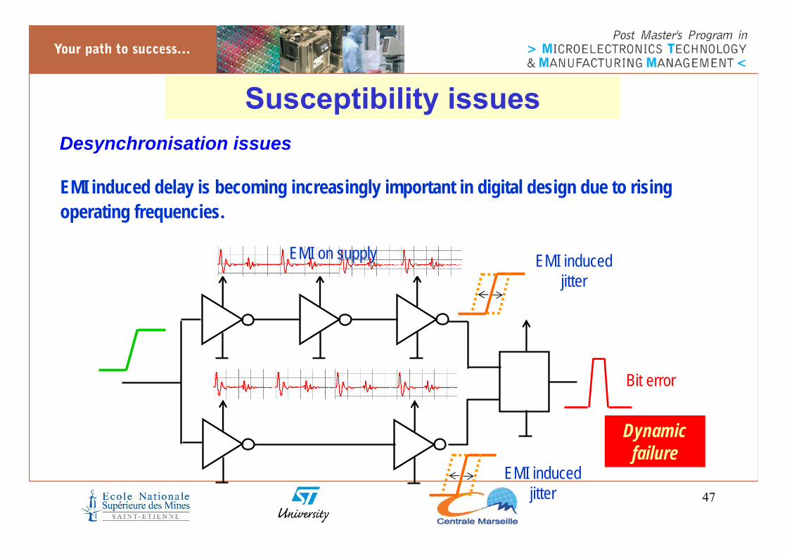
Susceptibility issuesDesynchronisation issues
EMI induced delay is becoming increasingly important in digital design due to rising operating frequencies.
EMI induced jitter
EMI induced jitter
Bit error
Dynamic failure
EMI on supply
48
IC failures
Origin of IC susceptibilityOverview of influent parameters on IC susceptibility
IC
IC Internalinterconnexions
IC active devices
PCB tracks andexternal passive
components
Vdd
Vss
RF interferences
Internal perceived noise
1. Filtering effects of PCB tracks and external passive components
2. Filtering effect of IC interconnections
3. Impedance of IC nodes (high Z node = high susceptibility)
4. Non linear effects of active devices (conversion RF signals to DC offsets !)
5. Block own susceptibility (noise margin, delay margin, …)
1
2 3 4 5

49
Emission / Susceptibility issues
--++3. Charge pump
+++1. DC/DC converter
++--7. Analog input/supply-+6. Digital block supply
-++5. Fast digital I/O
+++8. RF front end
++++4. Oscillator / PLL / Clock circuitry
--++2. Power switch output
SusceptibilityEmissionBlock type
Overview of typical emissive/susceptible blocks
1
2
3
48
56
7

50
4. EMC measurement methods

51
Why EMC standard measurement methods
Check EMC compliance of ICs, equipments and systemsComparison of EMC performances between different products, different technologies, designs, PCB routingsImprove interaction between customers and providers (same protocols, same set-up)
EMC measurement methods

52
Device under testCoupling deviceCoupling networkAntennasWave guide
Acquisition system
Spectrum analyzerEMI receiverOscilloscope
Emission – General measurement set-up
Radiated or conducted coupling
50Ω adapted path
Control -Acquisition
Emission requirements verified ?
Emission measurement methods

53
IEC 61967-2(GTEM 18 GHz)
IEC 61967-7(Mode Stirred Chamber: 18 GHz)
IEC 61967-5(WBFC, 1 GHz)
IEC 61967-4(1/150 ohm, 1 GHz)
IEC 61967-3/6(Near field scan, 5GHz)
IEC 61967-2(TEM : 1GHz)
International standards for IC emission measurement methods
Emission measurement methods
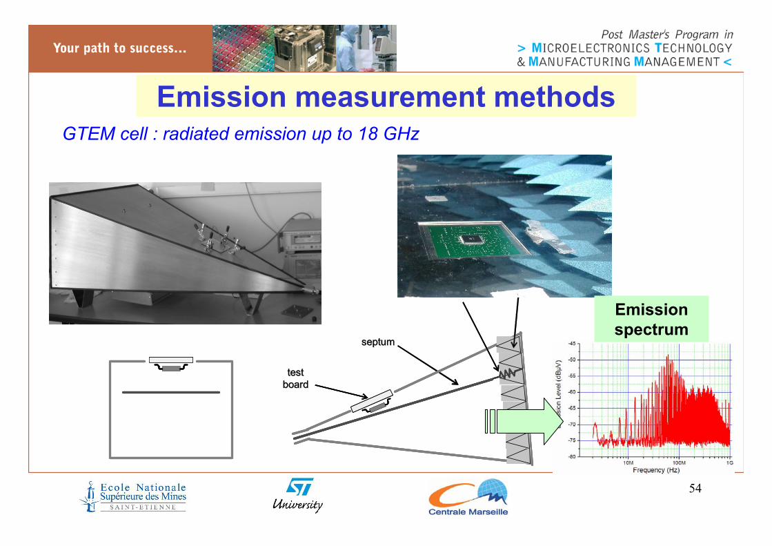
54
GTEM cell : radiated emission up to 18 GHz
septumseptum
test test boardboard
foam foam absorberabsorber
50 Ohms 50 Ohms resistive loadresistive load
septumseptum
test test boardboard
foam foam absorberabsorber
50 Ohms 50 Ohms resistive loadresistive load
Emission spectrum
Emission measurement methods

55
SpectrumAnalyser
1ohm
IC
Complex implementation
with multiple power pins
IEC 61967-4 International Standard : 1/150 Ohm method
Emission measurement methods
56
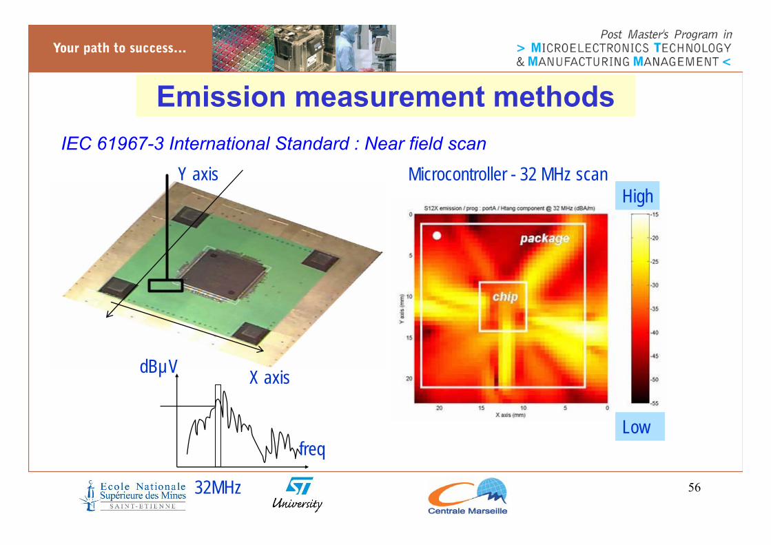
Microcontroller - 32 MHz scan
Low
High
X axis
Y axis
dBµV
freq
32MHz
IEC 61967-3 International Standard : Near field scan
Emission measurement methods

57
Hx Probe
Priviledgedcurrent
measurement
Power rails
CPU 12RAM2K
32K FEEPROM 28KFEEPROM
Power rails
MS-CAN
ATD1
ATD0
PWM
ECT
MIBUSMSI
EE1K
MMIINTBDM
KWU
LIM D60CGM
WCR
MEBIBKP
Emission measurement methodsIEC 61967-3 International Standard : Silicon scan
58
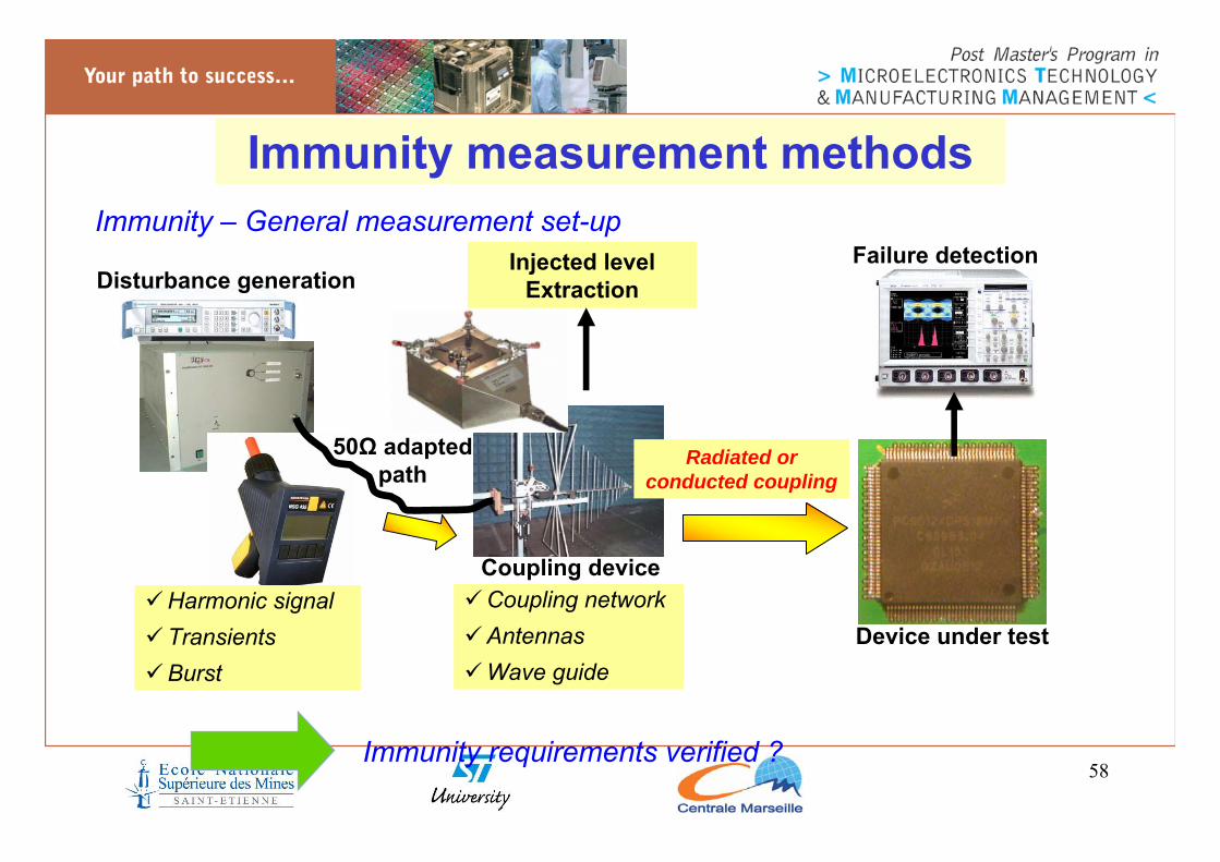
Immunity measurement methodsImmunity – General measurement set-up
Device under test
Coupling deviceCoupling networkAntennasWave guide
Radiated or conducted coupling
Disturbance generation
Harmonic signalTransientsBurst
50Ω adapted path
Failure detectionInjected level Extraction
Immunity requirements verified ?

59
Still research:(NFS 10 GHz)
New proposal: (LIHA : 10 GHz)
IEC 62132-5(WBFC 1 GHz)
IEC 62132-4(TEM/GTEM)
IEC 62132-3(Direct Power Inj 1GHz)
IEC 62132-2(Bulk Current Injection : 1 GHz)
International standards for IC susceptibility measurement methods
Immunity measurement methods
60
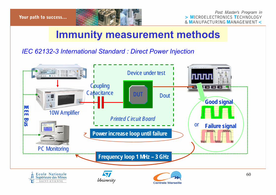
Immunity measurement methods
10W Amplifier
Oscilloscope
PC Monitoring
Signal generator
IEEE Bus or
Good signal
Failure signalPrinted Circuit Board
Device under test
DoutCoupling
Capacitance DUT
Power increase loop until failure
Frequency loop 1 MHz – 3 GHz
IEC 62132-3 International Standard : Direct Power Injection

61
Immunity measurement methods
Inductive coupling to the networkParasitic current injected on the chipLimited to 1 GHz
Normal current
Parasitic current
RF power
CAN Bus
Microcontroler
DUT
Fault
Measured current
IEC 62132-2 International Standard : Bulk Current Injection

62
EMC equipments
Vector Network Analyzer 10 GHz (100 K€)
Signal Synthesizer 6 GHz (20 K€) GTEM cell 18 GHz
(15 K€)
Spectrum analyzer 40 GHz (40 K€)
Amplifier 3 GHz 100W (60 K€)
Expensive ….Complete EMC laboratory : 500 K€
63
5. EMC guidelines

64
Basic concepts to reduce emission and susceptibility
Remember the influent parameters on emission and susceptibility
Control IC internal activity
Minimize circuit output load
Control effect of IC interconnections (decoupling)
Control effect of PCB interconnections (decoupling)
Emission: Susceptibility:
Control effect of PCB interconnections (decoupling)
Control effect of IC interconnections (decoupling)
Control Impedance of IC nodes
Reduce non linear effects of active devices
Improve block own susceptibility
Techniques used to reduce emission and/or susceptibility issues are based on these principles
Techniques used to reduce emission and/or susceptibility issues are based on these principles

65
Golden Rules for Low Emission
Lead: L=0.6nH/mm
Bonding: L=1nH/mm
• Inductance causes voltage bounce• Each conductor acts as an inductance• Ground plane modifies inductance value (worst case is far from ground)
A) Use shortest interconnection to reduce the serial inductance
Rule 1: Power supply routing strategy
Reducing inductance decreases voltage bounce !!
Reducing inductance decreases voltage bounce !!

66
Golden Rules for Low EmissionRule 1: Power supply routing strategy
A) Use shortest interconnection to reduce the serial inductance
Leadframe package:L up to 10nH
PCB
Long leads
Die of the IC
Close from ground
bonding
Die of the ICShort leads
ballsFlip chip package:L up to 3nH
Far from ground
Requirements for high speed microprocessors : L < 50 pH !Requirements for high speed microprocessors : L < 50 pH !

67
Golden Rules for Low EmissionRule 1: Power supply routing strategy
CorrectFail
9 I/O ports
B) Place enough supply pairs: Use One pair (VDD/VSS) for 10 IOs
68
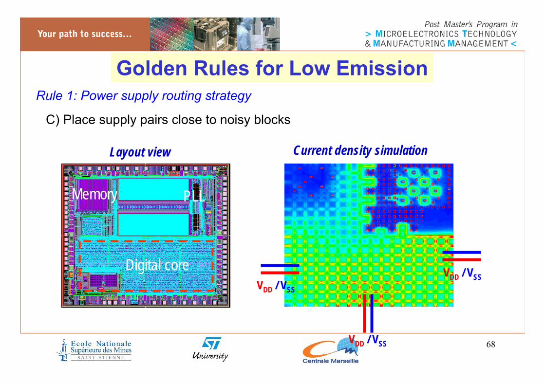
Golden Rules for Low EmissionRule 1: Power supply routing strategy
Current density simulation
C) Place supply pairs close to noisy blocks
Layout view
Digital core
Memory PLL
VDD / VSS
VDD / VSSVDD / VSS
69
Golden Rules for Low EmissionRule 1: Power supply routing strategy
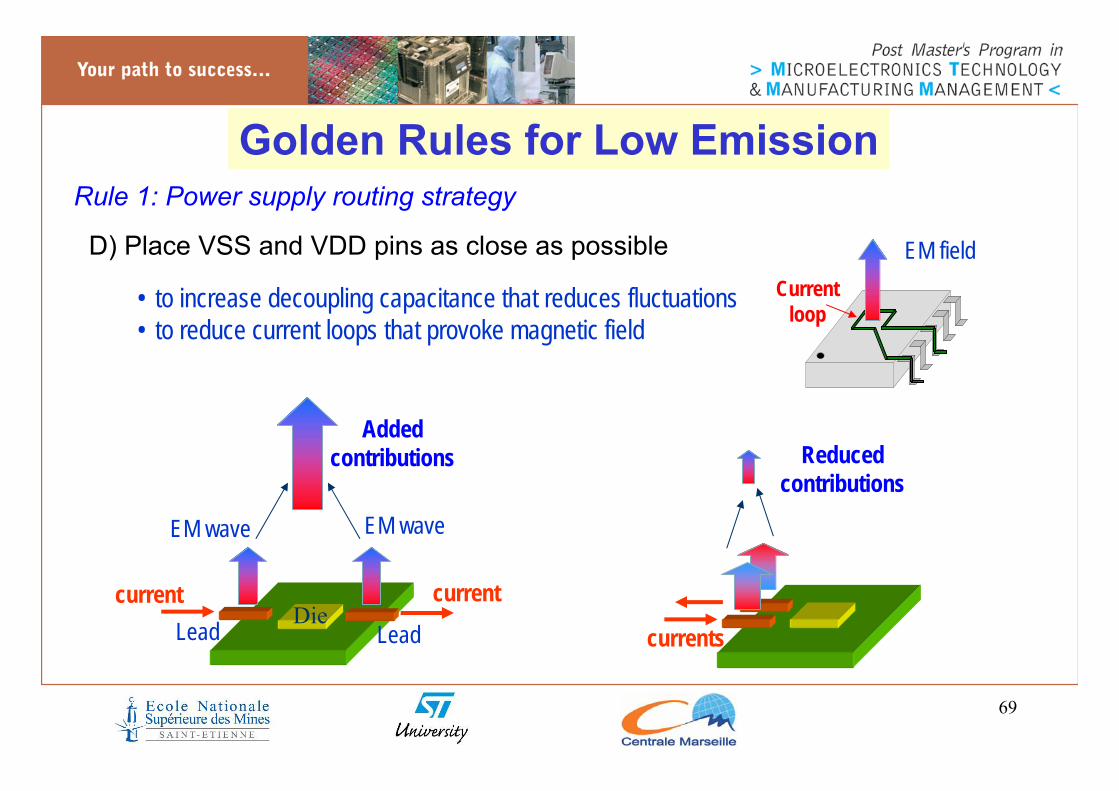
• to increase decoupling capacitance that reduces fluctuations• to reduce current loops that provoke magnetic field
D) Place VSS and VDD pins as close as possibleCurrent
loop
EM field
Added contributions
currentsDie
LeadLeadcurrent
EM wave
current
EM wave
Reduced contributions

70
Golden Rules for Low EmissionRule 1: Power supply routing strategy
Case 1 : Infineon Tricore Case 2 : virtex II
Case study 1:

71
Golden Rules for Low EmissionRule 1: Power supply routing strategy
Case study 2:
courtesy of Dr. Howard Johnson, "BGA Crosstalk", www.sigcon.com
• More Supply pairs for IOs
• Better distribution
• More Supply pairs for IOs
• Better distribution
2 FPGA , same power supply, same IO drive, same characteristicsSupply strategy very different !

72
Golden Rules for Low EmissionRule 1: Power supply routing strategy
Case study 2:
courtesy of Dr. Howard Johnson, "BGA Crosstalk", www.sigcon.com
Case 1: low emission due to a large number of supply
pairs well distributed
Case 1: low emission due to a large number of supply
pairs well distributed
Case 2: higher emission level (5 times higher)
Case 2: higher emission level (5 times higher)
73
Z Vdd - Vss
Frequency
Target impedance Zt (0.25 mΩ)
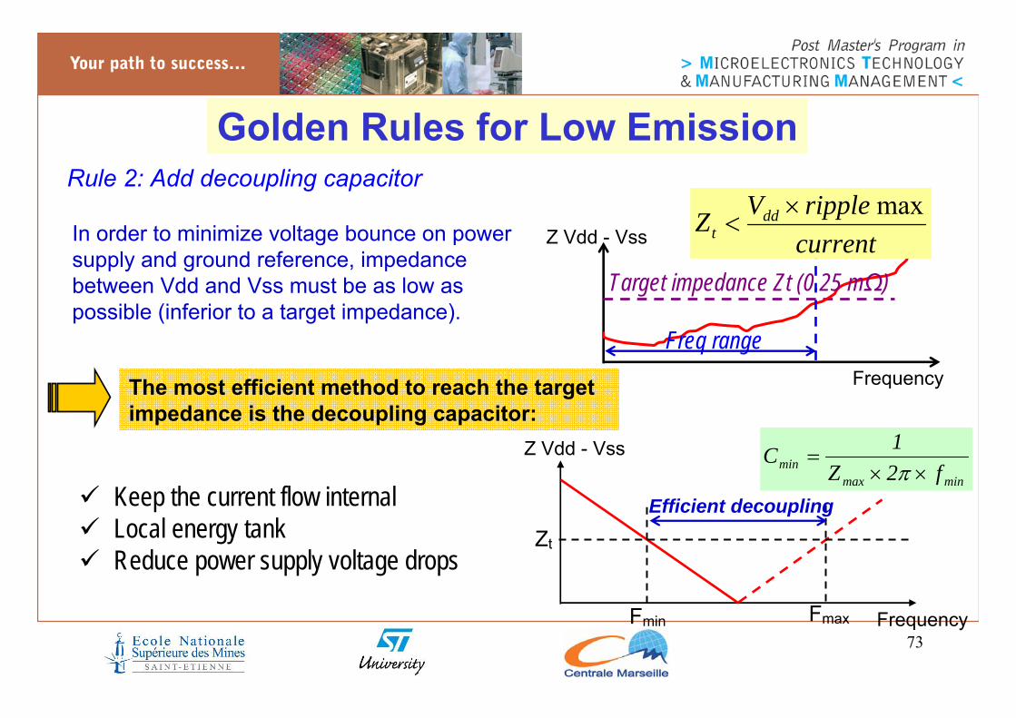
In order to minimize voltage bounce on power supply and ground reference, impedance between Vdd and Vss must be as low as possible (inferior to a target impedance).
Freq range
currentrippleVZ dd
tmax×
<
Keep the current flow internal Local energy tankReduce power supply voltage drops
Golden Rules for Low EmissionRule 2: Add decoupling capacitor
The most efficient method to reach the target impedance is the decoupling capacitor:
minmaxmin f2Z
1C××
=π
Z Vdd - Vss
Frequency
Zt
Fmin Fmax
Efficient decoupling

74
Golden Rules for Low EmissionRule 2: Add decoupling capacitor
Parasitic emission (dBµV)
-100
1020304050607080
1 10 100 1000Frequency (MHz)
Customer’s specification
No decoupling
No decoupling 10 – 15 dB
Volt
time
Internal voltage drop
10-100 nFdecoupling 10-100 nF
decoupling
time Efficient on one decadeEfficient on one decade
75
Voltage regulator
Power supply
Ground
On chip interconnections
Vdd
Vss
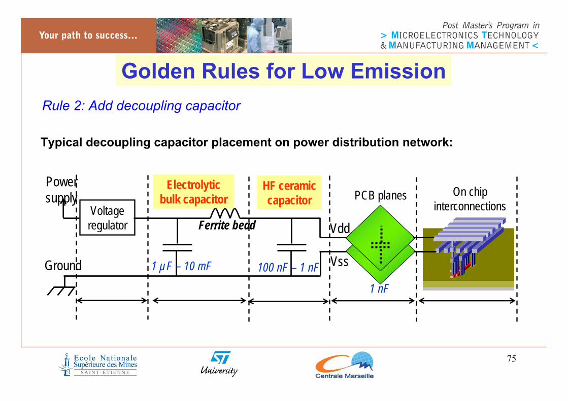
PCB planesElectrolytic
bulk capacitorHF ceramic capacitor
1 µF – 10 mF 100 nF – 1 nF
Ferrite bead
Golden Rules for Low EmissionRule 2: Add decoupling capacitor
Typical decoupling capacitor placement on power distribution network:
1 nF

76
Golden Rules for Low EmissionRule 2: Add decoupling on-chip capacitor
On chip decoupling capacitance versus technology and complexity
Devices on chip
Intrinsic on-chip supplycapacitance
100K 1M 10M
10pF
100pF
1.0nF
10nF
100M 1G
100nF
0.35µm0.18µm
90nm65nm
Very high efficient decoupling above 100 MHz (where PCB decoupling capacitors become inefficient) …… But space consumingFill white space with decap cellsUse MOS capa. or Metal-Insulator-Metal (MIM) capa.
Capa cell for local decoupling

77
Golden Rules for Low EmissionRule 3: Reduce core noise
Reduce operating supply voltageReduce operating frequencyReduce peak current by optimizing IC activity:
using distributed clock buffers
turning off unused circuitry
avoiding large loads
using several operation mode
Parasitic emission (dBµV)
01020304050607080
1 10 100 1000Frequency (MHz)

78
Golden Rules for Low EmissionRule 3: Reduce core noise
Clock in
T Pseudorandom noise
f
P
+/-Δf
+/-Δf
Clock out
T+/-Δt
Spread spectrum frequency modulation
1/T
specification
f
•Add a controlled jitter on clock signal to spread the noise spectrum

79
Golden Rules for Low EmissionRule 3: Reduce core noise
datarequest
acknowledgment
Asynchronous block
data
clock
Synchronous block
1/T
specification
f
• Asynchronous design spreads noise on all spectrum (10 dBµV reduction)

80
Golden Rules for Low EmissionRule 4: Reduce I/O noise
•Minimize the number of simultaneous switching lines (bus coding)•Reduce di/dt of I/O by controlling slew rate and drive
f
SR
Emission level
Tr1 Tr2
1/Tr11/Tr2

81
Golden Rules for Low Susceptibility
Work done at Eseo France (Ali ALAELDINE)
Immunity level (dBm)
Frequency
No rules to reduce susceptibility
Substrate isolation
Decoupling capacitance• DPI aggression of a digital core
• Reuse of low emission design rules for susceptibility
• Efficiency of on-chip decoupling combined with resistive supply path
• DPI aggression of a digital core
• Reuse of low emission design rules for susceptibility
• Efficiency of on-chip decoupling combined with resistive supply path
Rule 1: Add decoupling capacitance

82
Golden Rules for Low SusceptibilityRule 2: Isolate Noisy blocks
Analog
Standardcells
Noisy blocks
Far fromnoisy blocks
Bulk isolation
Separate supply
Why ? • To reduce the propagation of
switching noise inside the chip• To reduce the disturbance of
sensitive blocks by noisy blocks (auto-susceptibility)
How ?• by separate voltage supply• by substrate isolation• by increasing separation between
sensitive blocks• By reducing crosstalk and
parasitic coupling at package level
83
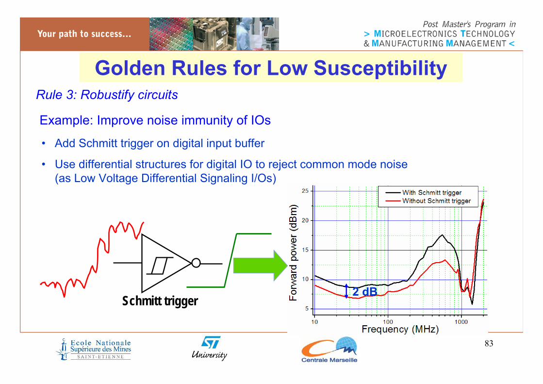
Golden Rules for Low SusceptibilityRule 3: Robustify circuits
• Add Schmitt trigger on digital input buffer
• Use differential structures for digital IO to reject common mode noise (as Low Voltage Differential Signaling I/Os)
Schmitt trigger2 dB
Example: Improve noise immunity of IOs

84
Golden Rules for Low SusceptibilityRule 3: Robustify circuits
Work done at INSA Toulouse/TIMA Grenoble(Fraiddy BOUESSE)
• Synchronous design are sensitive to propagation delay variations due to EMI ( dynamic errors)
• Improve delay margin to reduce desynchronization failures in synchronous design
• Asynchronous logic design is less sensitive to delay compared to synchronous design
15 dB
Reduce desynchronisation issues:

85
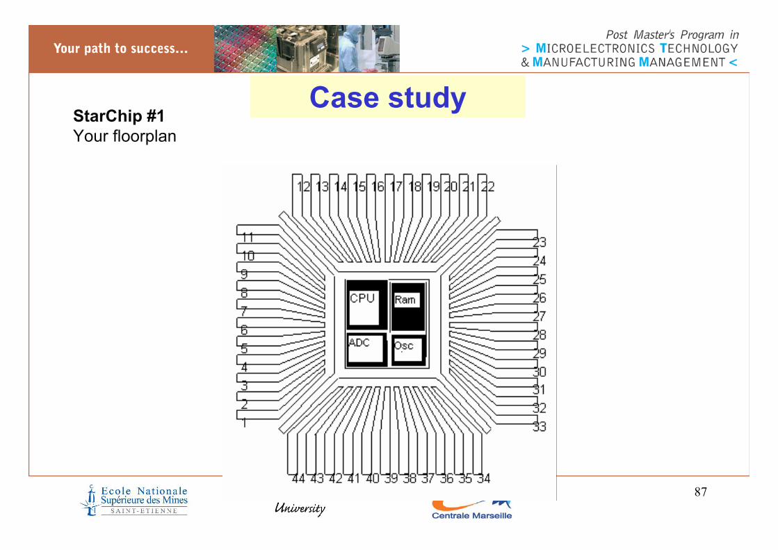
Case studyStarChip #1 Your definitive solution for embedded electronics,16 bit MPU with 16 MHz external quartz,
Reset microcontrollerRESET
PLL external capacitanceCAPA
Quartz oscillator 16MHzXTL_1, XTL_2
CAN interface (high power, 1MHz)CAN Rx
CAN interface (high power, 1MHz)CAN Tx
4 analog inputs (12 bit resolution)ADC In [0..3]
Data port C (programmable drive) external 66MHz data/addressPC[0..7]
Data port B (programmable drive) PB[0..7]
Data port A (programmable drive)PA[0..7]
Oscillator groundVSS_OSC
Oscillator supplyVDD_OSC
Logic GroundVSS
Positive supplyVDD
DescriptionSIGNAL
Emission Susceptible
• on-chip PLL providing internal 133MHz operating clock.• 128Kb RAM, 3 general purpose ports (A,B,C, 8bits)• 4 analog inputs 12 bits, CAN interface

86
VSS
PortA PortB
OSC
VDD
VDD_Osc
VSS_Osc
PortC
ADC [0..3] CA
Reset
NC
Capa
NC
NC
NC
Case studyStarChip #1 Initial floorplan
87
Case studyStarChip #1 Your floorplan
88
6. Conclusion

89
With technology scale down, ICs become more sensitive and emissive.
EMC of ICs has become a major concerns for ICs suppliers
Basic concepts are necessary to make preliminary analysis of EMCproblems and propose first solutions
Origins of emission and susceptibility issues at IC level have been described. Their knowledge is required to apply EMC design guidelines.
The classical EMC design guidelines at IC level have been presented: reducing inductances, adding decoupling capacitor, reducing core activity, robustifycircuits, isolating noise blocks from sensitive blocks).
Conclusion

90
Electromagnetic Compatibility of Electromagnetic Compatibility of Integrated Circuits (EMC of ICs)Integrated Circuits (EMC of ICs)
Part II Part II –– Lab ActivityLab Activity
91
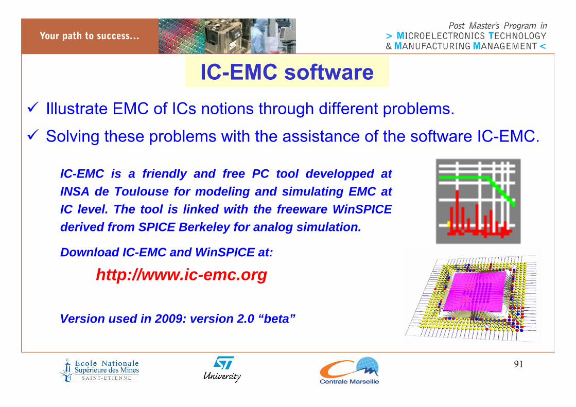
IC-EMC softwareIllustrate EMC of ICs notions through different problems.
Solving these problems with the assistance of the software IC-EMC.
IC-EMC is a friendly and free PC tool developped at INSA de Toulouse for modeling and simulating EMC at IC level. The tool is linked with the freeware WinSPICEderived from SPICE Berkeley for analog simulation.
Download IC-EMC and WinSPICE at:
http://www.ic-emc.org
Version used in 2009: version 2.0 “beta”

92
IC-EMC main screen
Symbol palette
Schematic capture interface
IC-EMC simulation tools
Simulation command

93
Simulation flow with IC-EMCIC-EMC schematic
Editor (.sch)IC-EMC model
libraries
WinSPICE compatible netlist generation (.cir)
WinSPICE simulation
IC-EMC Post-processing tools (emission, impedance,
S-parameters, immunity)
Measurement result files import
Output file generation

94
Most important icons
Symbol paletteAdd a lineIbis file editorAdd Text line
S parameter simulationFlip symbols
View all schematicView electrical net
Impedance simulationRotate symbols
Time domain analysisMove symbols
Immunity simulationCopy symbols
Near field emission simu.Delete symbols
Spectrum analysisSave schematic (.sch)
Build SPICE netlist (.cir)Open schematic (.sch)

95
SPICE simulation
WinSPICE interface:
Click File/Open to open a circuit netlist (.cir) generated by ic-emc.
When the netlist is opened, each time the netlist is regenerated, a simulation is launched again.
Main simulation commands for IC-EMC:
sampling + nb points + start + stop
.AC LIN/DEC 100 1MEG 1GSmall signal freq. analysis
.lib spice_lib.lib
.DC Vdd 0 5 0.1
.tran 0.1n 100nCommand line
Path and file nameLoad SPICE library
source + start + stop + stepDC simulationstep + stop timeTransient simulationParametersSimulation command
96
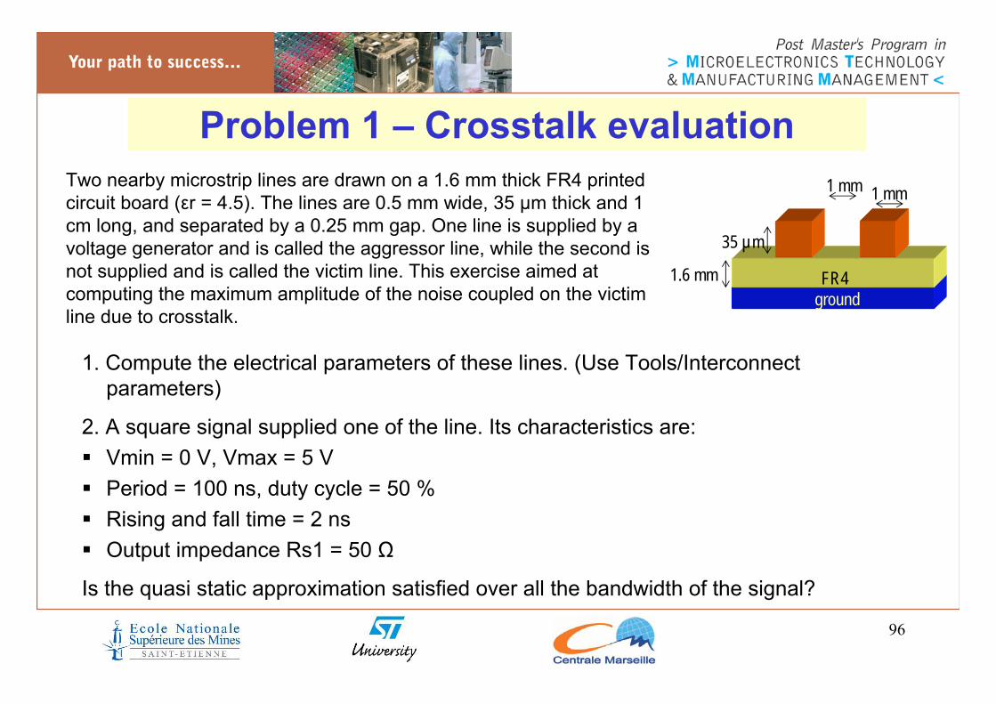
Problem 1 – Crosstalk evaluation
FR4ground
1.6 mm
35 µm
1 mm1 mmTwo nearby microstrip lines are drawn on a 1.6 mm thick FR4 printed circuit board (εr = 4.5). The lines are 0.5 mm wide, 35 µm thick and 1 cm long, and separated by a 0.25 mm gap. One line is supplied by a voltage generator and is called the aggressor line, while the second is not supplied and is called the victim line. This exercise aimed at computing the maximum amplitude of the noise coupled on the victim line due to crosstalk.
1. Compute the electrical parameters of these lines. (Use Tools/Interconnect parameters)
2. A square signal supplied one of the line. Its characteristics are:Vmin = 0 V, Vmax = 5 VPeriod = 100 ns, duty cycle = 50 %Rising and fall time = 2 nsOutput impedance Rs1 = 50 Ω
Is the quasi static approximation satisfied over all the bandwidth of the signal?

97
Problem 1 – Crosstalk evaluationAggressor line
Victim lineV1
RS1
RS2
RL1
RL2
VNE VFE
3. The 3 other input/output ports of these 2 lines are loaded by 50 Ω resistors. VFE and VNE are the far end and near end voltage. Propose an equivalent electrical schematic of these coupled lines.
4. Propose an equivalent model for the victim line. Deduce literal expressions of far end and near end peak voltage on the victim line.
5. Verify your expression in simulation.
6. Could this parasitic coupling involve EMC problems?
7. Is the literal expressions are still valid for a 10 cm line ?

98
Problem 2 – Simultaneous switching noise
Let’s consider the case of the following single output buffer. It is modelled as a CMOS inverter with the given dimensions. Models of MOS transistors are included in the file lib_SPICE.lib. This buffer is driven by a predriver stage that we model as a square generator with the following characteristics:
V0 = 0 V, V1 = 5 V
Tr = Tf = 1 ns
Period = 100 ns
PW = Period – Tr (to keep a 50 % duty cycle)
The output buffer will be loaded with a capacitance. The conducted noise on supply lines will be probed with a 1 Ω resistor placed on Vss path of the buffer.
1. Build the schematic of the I/O loaded by 10 pF. Observe the transient response across the 1 Ω probe. Comment. Deduce the amplitude of dynamic consumption of current.

99
Problem 2 – Simultaneous switching noise
2. Load the output of the buffer with different values of capacitance (from 10 fF to 1 nF). Observe the transient response of voltage across the 1 Ω probe and comment.
3. Load the output with a 47 pF capacitor. Plot the FFT of the voltage across Vss. What is the bandwidth of the noise ?
4. Do the simulation of question 3 for Tr = 5 ns. Comment the result.
5. The load is connected to the buffer through a 4 cm long, 0.5 mm wide tracks drawn on a 1.6 mm FR4 PCB. Inductance of the package is estimated about 6 nH. Observe the transient response and the spectrum of voltage across the 1 Ω probe and comment.
6. Inductance on power supply and ground reference are estimated at 10 nH (PCB planes and package). Does it influence the power integrity?
7. Simulate the noise on ground reference for a 8 I/O port. Propose a solution to reduce the noise amplitude.

100
Problem 3 – Digital core conducted emission
To predict parasitic emission of digital core of integrated circuits, macromodelling as ICEM model (IEC 62433) is often used to provide accurate results with a low complexity model. It simplifies the activity of a digital core to one or several equivalent current sources and the complex power distribution network to a passive network composed of several R, L, C elements.
IC-EMC provides a tool called ICEM model expert (Tools/ICEM model expert) which helps generating ICEM model of a digital circuit based on basic information.
Let’s consider the following 16 bit microcontroller:StandardPerformance
1number of core supply pairs
QFPPackage
15 mm²IC size
0.1 ohmEmission measurement
15 %Gate activity
100 KNumber of gates
20 MHzBus clock frequency
1.2 VCore supply voltage
0.12 µmTechnology
1. Use the tool ICEM model expert to generate the ICEM model of this microcontroller. Simulate the voltage noise measured across the 0.1 Ω probe. What information does this voltage provide ?

101
2. Simulate the IC internal power supply and ground voltage. Is the voltage references are acceptable for a safe operation ?
3. The constraint in term of maximum emission level from 150 KHz to 1 GHz is defined as ‘H8’ (definition from standard IEC71967). What is the effect of 2 additional supply pairs on conducted noise ? On internal noise ?
4. A “traditional” 100 nF ceramic capacitor external capacitor is added. Its real model includes a serial 0.5 nH inductor and a 100 mΩ resistor. Effect of PCB is neglected. Trace its impedance profile between 1 MHz and 1 GHz. On which frequency band this capacitor decouples efficiently? What is its effect on the conducted emission ? On the internal noise ?
5. Add further external decoupling capacitances (keep the same values for R and L values for capacitance parasitics). Adjust their numbers and their values to ensure the specification in term of emission.
6. Adjust the internal activity to reduce the emission level enough to satisfy the maximum emission criterion.
Problem 3 – Digital core conducted emission

102
Problem 4 – Decoupling and conducted emission
The circuit describes in problem 3 is mounted on a 2 layers PCB. The following schematic describes the top layer of the PCB, where the components are mounted. The bottom side is a full ground plane. Characteristics of the PCB is: FR4 (εr = 4.6, height = 1.6 mm).
All the components are surface mounted devices. The schematic describes the connection of Vdd and Vss pins of the circuit to the power supply and ground references assured by a regulator. These references are supposed ideal. A 0.1 Ω resistor is added across the Vss pin.
Regulator
Circuit
0.1 Ω
= via
W=1 mm, L=5 cm
W=0.5 mm, L=5 mm
Gnd
Vcc Vcc
Vss
1. Build the equivalent model of the circuit (use Tools/ICEM model expert) and the PCB (use Tools/Interconnect parameters). Simulate the voltage measured across the 0.1 Ωprobe. What information does this voltage provide ?

103
Problem 4 – Decoupling and conducted emission
2. The constraint in term of maximum emission level from 150 KHz to 1 GHz is defined as ‘H8’ (definition from standard IEC71967). Does the circuit check the conducted emission requirements ?
3. 1 ceramic 100 nF capacitor is a typically used as decoupling capacitor for digital circuits. Place a 100 nF capacitor close to the circuit. What is the effect on the conducted noise ?
4. Is the previous model realistic ? Add a more realistic model of capacitor. Test the placement of the capacitor.
5. Simulate the impedance seen from the pins Vdd/Vss of the circuit with and without the 100 nF decoupling capacitor. What is the link with the conducted emission ?
6. Add several decoupling capacitor to make the circuit compliant to the conducted emission requirements.
104
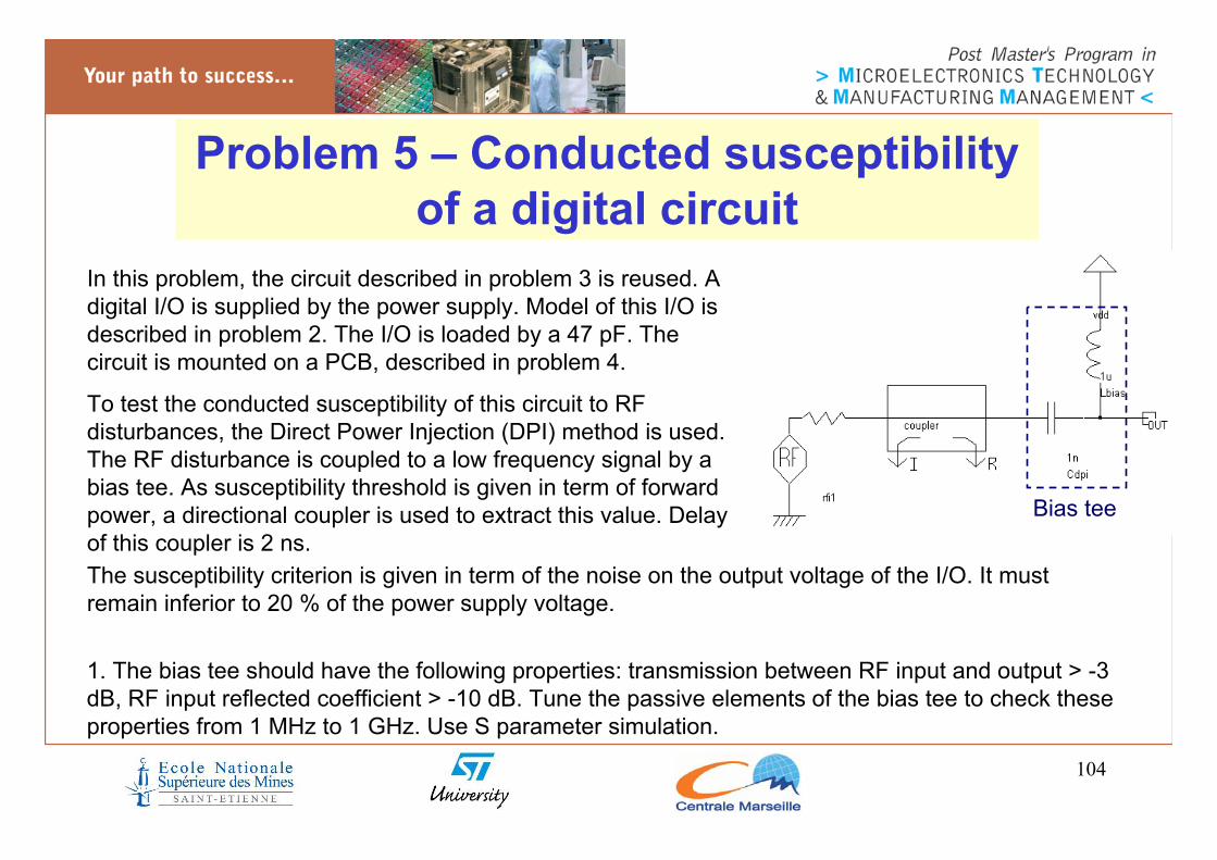
Problem 5 – Conducted susceptibility of a digital circuit
In this problem, the circuit described in problem 3 is reused. Adigital I/O is supplied by the power supply. Model of this I/O is described in problem 2. The I/O is loaded by a 47 pF. The circuit is mounted on a PCB, described in problem 4.
To test the conducted susceptibility of this circuit to RF disturbances, the Direct Power Injection (DPI) method is used. The RF disturbance is coupled to a low frequency signal by a bias tee. As susceptibility threshold is given in term of forward power, a directional coupler is used to extract this value. Delay of this coupler is 2 ns.
Bias tee
The susceptibility criterion is given in term of the noise on the output voltage of the I/O. It must remain inferior to 20 % of the power supply voltage.
1. The bias tee should have the following properties: transmission between RF input and output > -3 dB, RF input reflected coefficient > -10 dB. Tune the passive elements of the bias tee to check these properties from 1 MHz to 1 GHz. Use S parameter simulation.

105
Problem 5 – Conducted susceptibility of a digital circuit
2. Connect the bias tee and the RF injection system to a 100 Ω load. Simulate the susceptibility threshold for a maximum noise of 1 V across the load. Would it be possible to predict the susceptibility threshold without SPICE simulation ?
3. Build the equivalent model of the circuit (use Tools/ICEM model expert) and the PCB (use Tools/Interconnect parameters, remove the 1 Ω probe). Simulate the susceptibility threshold of circuit.
4. Simulate the reflection coefficient of the circuit. Does a link exist between the susceptibility threshold and the reflection coefficient ?
5. If a decoupling capacitor is added between Vdd and Vss, what will be the effect on circuit susceptibility ? Verify your conclusion by simulation.