
ELECTRICAL PROPERTIES AND DEVICE APPLICATIONS OF ATOMIC ... · ELECTRICAL PROPERTIES AND DEVICE...
85
ELECTRICAL PROPERTIES AND DEVICE APPLICATIONS OF ATOMIC LAYER DEPOSITED ZnO AND GaN THIN FILMS A THESIS SUBMITTED TO THE DEPARTMENT OF ELECTRICAL AND ELECTRONICS ENGINEERING AND THE GRADUATE SCHOOL OF ENGINEERING AND SCIENCE OF BILKENT UNIVERSITY IN PARTIAL FULLFILMENT OF THE REQUIREMENTS FOR THE DEGREE OF MASTER OF SCIENCE By Sami Bolat August, 2014
Transcript of ELECTRICAL PROPERTIES AND DEVICE APPLICATIONS OF ATOMIC ... · ELECTRICAL PROPERTIES AND DEVICE...

ELECTRICAL PROPERTIES AND DEVICE
APPLICATIONS OF ATOMIC LAYER
DEPOSITED ZnO AND GaN THIN FILMS
A THESIS
SUBMITTED TO THE DEPARTMENT OF ELECTRICAL AND
ELECTRONICS ENGINEERING
AND THE GRADUATE SCHOOL OF ENGINEERING AND SCIENCE
OF BILKENT UNIVERSITY
IN PARTIAL FULLFILMENT OF THE REQUIREMENTS
FOR THE DEGREE OF
MASTER OF SCIENCE
By
Sami Bolat
August, 2014

ii
I certify that I have read this thesis and that in my opinion it is fully adequate, in
scope and in quality, as a thesis for the degree of Master of Science.
Assist. Prof. Dr. Ali Kemal Okyay (Supervisor)
I certify that I have read this thesis and that in my opinion it is fully adequate, in
scope and in quality, as a thesis for the degree of Master of Science.
Prof. Dr. Mehmet Bayındır
I certify that I have read this thesis and that in my opinion it is fully adequate, in
scope and in quality, as a thesis for the degree of Master of Science.
Assist. Prof. Dr. Necmi Bıyıklı
Approved for the Graduate School of Engineering and Science:
Prof. Dr. Levent Onural
Director of Graduate School

iii
ABSTRACT
ELECTRICAL PROPERTIES AND DEVICE
APPLICATIONS OF ATOMIC LAYER DEPOSITED ZnO
AND GaN THIN FILMS
Sami Bolat
M.S. in Electrical and Electronics Engineering
Supervisor: Assist. Prof. Dr. Ali Kemal Okyay
August, 2014
Zinc oxide (ZnO), a semiconducting material with a wide band gap of 3.37 eV,
has become a promising material for wide range of electronic and optoelectronic
applications. One of the most important properties of this material is its large
exciton binding energy of 60 meV, which makes ZnO a strong candidate for
ultraviolet light emitting diodes and lasers. In addition, potentially high electron
mobility and the transparency in the visible region strengthen the future of the
ZnO based transparent electronics. Although several applications of ZnO have
taken their places in the literature, use of ZnO in the thermal imaging
applications is yet to be explored.
In the parts of this thesis related to ZnO, the temperature coefficient of
resistance and electrical noise together with resistivity and contact resistance
properties of atomic layer deposition based ZnO are investigated. Due to its
remarkably high temperature coefficient of resistance value and suitable 1/f
noise corner frequency, this material is proposed as an alternative material to be
used in the active layers of uncooled microbolometers.
GaN is another wide gap semiconductor which has been intensely investigated
throughout the last decades for its potential usage in both optical and electrical
applications. Especially, high saturation velocity of the electric carriers of this
material has made it a strong candidate to be used in high power applications.

iv
Furthermore the high electron mobility transistors based on the 2-dimensional
electron gas region formed between the AlGaN and GaN, have found wide
range of applications in radio frequency (RF) electronics area. Currently, most
commonly used techniques for growing GaN, are metal organic chemical vapor
deposition and molecular beam epitaxy. Both of these techniques offer single
crystalline layers; however, the process temperatures used in the growth of the
GaN disable the use of this material in low temperature flexible
electronic/optoelectronic applications. In order to solve this problem, hollow
cathode plasma assisted atomic layer deposition technique is utilized and GaN
thin films with polycrystalline structures are successfully grown at 200°C.
In the parts of this thesis related to GaN, the electrical properties, the effect of
contact annealing on the resistivity of the GaN thin films and the contact
resistance between this material and Ti/Au metallization scheme are
investigated. Afterwards, we present the world’s first thin film transistor with
atomic layer deposition based GaN channel and discuss its electrical
characteristics in detail. Finally, the GaN thin film transistors are fabricated by
performing all fabrication steps at temperatures below 250°C. This is the lowest
process thermal budget for the GaN based thin film transistors reported so far.
Electrical characteristics as well as the stability of the proposed device are
investigated and the results obtained are discussed. Proposed devices are
believed to pave the way for the GaN-based stable flexible/transparent
electronics after further materials and process optimization.
Keywords: ZnO, GaN, atomic layer deposition, microbolometer, Thin Film
Transistor

v
ÖZET
ATOMİK KATMAN KAPLAMA METODU İLE
BÜYÜTÜLEN ZnO ve GaN İNCE FİLMLERİN
ELEKTRİKSEL ÖZELLİKLERİ VE AYGIT
UYGULAMALARI
Sami Bolat
Elektrik ve Elektronik Mühendisliği Bölümü Yüksek Lisans
Tez Yöneticisi: Yrd. Doç. Dr. Ali Kemal Okyay
Ağustos, 2014
3.37 eV bant aralığına sahip olan çinko oksit, ZnO birçok elektronik ve opto-
elektronik uygulama için gelecek vaad eden bir materyaldir. Bu materyalin en
önemli özelliklerinden biri yüksek eksiton bağlanma enerjisi (60 meV) olup bu
özellik çinko oksidi mor ötesi ışık yayan diyotlar ve lazerler için güçlü bir aday
malzeme yapar. Buna ek olarak yüksek elektron hareketliliği ve gözle görünür
dalga boylarında saydam olması ZnO tabanlı saydam elektronik uygulamaların
potansiyelini güçlendirmektedir. Her ne kadar çok çeşitli uygulamalarda
kullanılabilirliği test edilmiş olsa da, şu ana kadar bu materyalin termal
görüntüleme alanlarındaki uygulaması çalışılmamıştır.
Bu tezin ZnO ile ilgili kısımlarında, atomik katman kaplama tabanlı ZnO ince
filmlerin özdirençleri, bu filmlerin çeşitli metallerle aralarında olan kontak
direnci, sıcaklığa bağlı direnç değişim katsayısı (TCR) ve bu filmlerin frekansa
bağlı elektriksel gürültü özellikleri araştırılmıştır. Bu materyalin, yüksek TCR
ve termal görüntülemeye uygun gürültü değerlerine sahip olduğu
gösterilmektedir. Bu özellikleri sayesinde, ZnO termal görüntüleme
uygulamalarında alternatif bir materyal olarak literatüre kazandırılmaktadır.
vi
GaN başka bir geniş bant aralığına sahip yarı iletken materyal olup geçtiğimiz
yıllar içerisinde elektriksel ve optik uygulamalarda kullanılabilirliği yoğun bir
şekilde araştırılmıştır. Özellikle bu materyalin elektronlarının sahip olduğu
yüksek doygunluk hızı, yüksek güç uygulamalarında GaN’ın kullanım
potansiyelini artırmıştır. Aynı zamanda çalışma prensibi AlGaN ve GaN
arasında oluşan 2 boyutlu elektron gazına dayanan yüksek elektron mobilite
transistorlar yüksek hız içeren uygulamalarda kendilerine önemli bir yer
edinmişlerdir. Günümüzde, GaN kaplaması için en sık kullanılan metotlar metal
organik kimyasal buhar kaplama metodu ve moleküler demet epitaksisidir. Bu
teknikler kullanıldığında yüksek kristal kalitesine sahip filmler elde edilmektedir
ancak, filmlerin kaplama sıcaklıkları uygulama alanlarını kısıtlamaktadır. Bu
materyali düşük sıcaklık kaplamaları içeren bükülebilir saydam elektronik
endüstrisine kazandırmak için oyuk katot plazma katkılı atomik katman kaplama
tekniği kullanılmıştır ve GaN ince filmler 200°C’de başarılı bir şekilde poli
kristal yapıya sahip olarak üretilmiştir.
Bu tezin GaN ile ilgili kısımlarında, ince filmlerin özdirençleri ve Ti/Au
metalleri ile sahip olduğu kontak dirençleri tavlamanın etkileri de eklenerek
incelenmiştir. Daha sonar atomik katman kaplama metodu ile kaplanan GaN
tabanlı ilk ince film transistor üretilmiş ve elektriksel karakterizasyon sonuçları
detaylı bir şekilde tartışılmıştır. Son olarak, literatürdeki bilinen en düşük
fabrikasyon sıcaklığına sahip ( kullanılan en yüksek kaplama sıcaklığı
250°C’dir. ) GaN kanallı ince film transistorlar üretilmiştir. Üretilen aygıtın
elektriksel özellikleri ve dayanıklılığı incelenmiş olup sonuçlar tartışılmıştır. Bu
çalışmanın, GaN tabanlı dayanıklı bükülebilir elektronik uygulamalarda öncü
çalışmalar olacağına inanılmaktadır.
Anahtar Kelimeler: ZnO, GaN, atomik katman kaplama, mikrobolometre, İnce
Film Tranzistör

vii
To my lovely sisters Cennet and Hasna Betül

viii
Acknowledgements
I am deeply thankful to Dr. Ali Kemal Okyay for his guidance throughout my
master’s degree studies. I have gained invaluable information from him in terms
of both theoretical and practical aspects of academic life. He has been a great
leader for me and all Okyay Group members. In addition, I would like to express
my deepest gratitudes to Dr. Mehmet Bayindir and Dr. Necmi Biyikli for being
in my thesis committee and increasing the quality of my thesis with their
comments and suggestions.
This work was supported by the Scientific and Technological Research Council
of Turkey (TUBITAK), grant numbers 109E044, 112M004, 112E052,
112M482, and 113M815. I would also like to thank TUBITAK-BIDEB for the
national MSc. scholarship.
I am in depth to my mentors Feyza Oruç and Fatih Bilge Atar. I have learned a
lot from them yet have never been able to thank them enough.
I would like to specially thank my lab buddies Burak Tekcan, Muhammad Maiz
Ghauri, Merve Marçalı, Levent Erdal Aygün, Yunus Emre Kesim, Mehmet
Alican Noyan, İnci Dönmez, Hamit Eren and Deniz Kocaay for the good
memories.
I would also like to thank Okyay Group members Enes Battal, Ayşe Özcan, Elif
Özgöztaşı, Furkan Çimen, Amin Nazirzadeh, Doğan Gül, Abdullah Gök, Şeyma
Canik, Şahin Beşerik and Mehrab Ramzan for being nice friends to me.
I would like to thank Berk Berkan Turgut, Bartu Şimşek, Elif Uzcengiz,
Fehmiye Keleş, Canan Kurşungöz and İsmail Kupa for the nice conversations
we had during the coffee breaks.

ix
I would like to thank Pelin Kübra İşgör, Lütfiye Hallıoğlu, Ayşegül Abdelal, and
Ebru Cihan, the members of the UNAM’s open air office (the office windows
were always open ), who have always been patient during my visits to their
office.
I would like to thank Demir Group Members Shahab Akhavan, Burak
Güzeltürk, Kıvanç Güngör, Yusuf Keleştemur, Halil Akçalı, İbrahim Akçalı,
Mehmet Zafer Akgül, Can Uran, Aydan Yeltik and Talha Erdem for being the
nicest neighbors to me.
I would like to thank my office friends Tolga Tarkan Ölmez, Ahmet Emin
Topal, Ömer Faruk Sarıoğlu, Ebuzer Kalyoncu, Ayşe Tezcan Özdemir, Yıdlız
Gözde Sağlam, and Alper Devrim Özkan for being nice to me and for their
patience against me (a noisy person).
I would also like to thank our collaborators Dr. Çağla Özgit-Akgün, Ali Haider,
Seda Kizir, Türkan Bayrak, Halil Volkan Hünerli and Dr. Eda Goldenberg for
their invaluable helps in my research.
I would also like to thank UNAM Cleanroom Team members, Semih Yaşar,
Fikret Piri and Abdullah Kafadenk.
I would like to specially thank Kamil Nar, Alican Yüksel, Özgür Yılmaz, Fırat
Öcal, Orhan Ahmet Çelik, Burak Hasırcıoğlu, and Ahmet Furkan Akdeniz for
the nicest moments we spent in İsa Demiray 105 and 121 in METU. I will never
forget those memories.
I would like to specially thank Yusuf Özgüner, Burak Caner Cihangir, Metin
Yiğit, and Osman Fehmi Beyazal ( M.D.’s with the bright futures) for their great

x
hospitality and for the nice time we have been spending together for the last 7
years.
I would like to specially thank Mehmet Emin Balyemez, an idealist police
captain with a heart full of the love for his country, for being my best friend
since the elementary school times.
For those whom I forgot to mention here, I am no less thankful to everybody I
met during the last two years of my life, but it would be impossible to write all
the names in here.
Finally, I would like to thank my father for being the ideal role model of my
whole life; my mother for filling my life with happiness and making it
meaningful, and to my sisters, who have always been my best friends. I would
especially like to thank them for the delicious Turkish coffees they prepared for
me in the middle of several nights.

xi
Contents
Acknowledgements VIII
List of Figures XIV
List of Tables XVI
1 Introduction 1
1.1 Atomic Layer Deposited ZnO: Properties and Applications ................. 1
1.1.1 Properties and Device Applications of ZnO ...................................... 1
1.1.2 Motivation.......................................................................................... 2
1.2 Device Applications of Hollow Cathode Plasma Assisted Atomic Layer
s Deposition (HCPA-ALD) Based GaN Thin Films .................................. 4
1.2.1 Properties and Device Applications of GaN ...................................... 4
1.2.2 Motivation.......................................................................................... 4
1.3 Thesis Overview ...................................................................................... 5
2 Theoretical Background 7
2.1 Electrical Properties of Semiconductors and the Properties of Metal-
scssdSemiconductor Ohmic Contacts .............................................................. 7
2.1.1 Resistivity .......................................................................................... 7
2.1.2 Contact Resistivity in Metal Semiconductor Junctions ................... 10
2.1.3 Temperature Dependent Resistances of Materials .......................... 13
2.1.4 Electronic Noise in Resistors ........................................................... 14

xii
2.2 Metal Oxide Semiconductor Field Effect Transistor (MOSFET) Basics
sdffff .............................................................................................................. 16
2.2.1 Operation Principles of MOSFETs .................................................. 16
2.2.2 Subthreshold Region ........................................................................ 19
2.3 Thin Film Transistors (TFTs) ................................................................ 19
3 Experimental Methods 21
3.1 Fabrication Equipments ......................................................................... 21
3.1.1 Plasma Enhanced Chemical Vapor Deposition (PECVD) .............. 21
3.1.2 Atomic Layer Deposition (ALD)..................................................... 22
3.1.3 Thermal Evaporator ......................................................................... 26
3.1.4 DC Magnetron Sputtering ............................................................... 27
3.1.5 Mask Aligner and Photolithography ................................................ 29
3.1.6 Inductively Coupled Plasma Reactive Ion Etching System (ICP-RIE)
s 31
3.2 Device Fabrication Steps ....................................................................... 33
3.2.1 Van Der Pauw Structures................................................................. 33
3.2.2 Cross Bridge Kelvin Resistors (CBKR) .......................................... 34
3.2.3 Thin Film Resistors with Interdigitated Contact Structures ............ 35
3.2.4 Bottom Gate Thin Film Transistors (BG-TFTs) .............................. 35
3.3 Electrical Characterization of the Devices ............................................. 37
3.3.1 Semiconductor Parameter Analyzer (SPA) ..................................... 37
3.3.2 Temperature Dependent Electrical Characterization Setup ............. 39
4 Electrical Properties of Atomic Layer Deposition Based ZnO Thin Films
d 40
4.1 Contact resistance of the Metal/ZnO junctions ...................................... 40
4.2 Resistivity of the Atomic Layer Deposited ZnO ................................... 43
4.3 Temperature Dependent Electrical characteristics of ALD grown ZnO 45
4.3.1 Temperature Coefficient of Resistance (TCR) ................................ 45
4.3.2 Flicker Noise .................................................................................... 48
xiii
5 Electrical Properties and Device Applications of Hollow Cathode Plasma
sdAssisted Atomic Layer Deposition (HCPA-ALD) Based GaN Thin Films
s
5.1 NH3 Plasma Assisted Atomic Layer Deposited GaN Thin Films .......... 51
5.1.1 Electrical Properties ....................................................................... 52
5.1.2 Bottom Gate Thin Film Transistors with NH3 Plasma Assisted sdc
scdscds Atomic Layer Deposited GaN Thin Films ..................................... 53
5.2 Bottom Gate Thin Film Transistors with N2/H2 Plasma Assisted Atomic
s Layer Deposited GaN Thin Films .......................................................... 56
6 Conclusion 61
Bibliography

xiv
List of Figures
Figure 2.1 Four point probe measurement method .............................................. 8
Figure 2.2 Van Der Pauw Structure ..................................................................... 9
Figure 2.3 TLM measurement structure ............................................................. 11
Figure 2.4 Measured resistance values for different contact spacings. ............... 11
Figure 2.5 CBKR structure ................................................................................. 13
Figure 2.6 Crossectional view of an n-channel MOSFET structure ................... 16
Figure 2.7 SEM image of the top view of the fabricated TFT ........................... 20
Figure 3.1 Vaksis Handy CVD/PECVD system ............................................... 22
Figure 3.2 Cambridge NanoTech Savannah 100 Atomic Layer Deposition
System ................................................................................................................ 23
Figure 3.3 Step by step demonstration of one ALD cycle of ZnO growth ........ 24
Figure 3.4 Cambridge NanoTech Fiji F200 PEALD Reactor ........................... 25
Figure 3.5 Vaksis MiDAS Thermal Evaporator PVD/3T .................................. 26
Figure 3.6 Vaksis MiDAS Magnetron Sputtering PVD/4M ............................... 28
Figure 3.7 EVG 620 Mask Aligner ..................................................................... 31
Figure 3.8 STS 615-616 ICP RIE Systems ........................................................ 32
Figure 3.9 Fabrication steps of Van Der Pauw structures .................................. 33
Figure 3.10 Fabrication steps of CBKR structures ............................................. 34
Figure 3.11 Fabrication steps of the resistors with interdigitated contact
structures ............................................................................................................ 35
Figure 3.12 Fabrication steps of the bottom gate thin film transistors ............... 37

xv
Figure 3.13 Keithley 4200 Semiconductor Parameter Analyzer and Probe
Station ................................................................................................................. 38
Figure 3.14 TCR Measurement Set-up ............................................................... 39
Figure 4.1. SEM image of the CBKR structure ................................................. 41
Figure 4.2 SEM image of the Van Der Pauw Structure ..................................... 43
Figure 4.3 SEM image of a thin film resistor having interdigitated contact
structure .............................................................................................................. 45
Figure 4.4 Temperature dependent resistance characteristics of 120°C grown
ZnO thin film. ..................................................................................................... 46
Figure 4.5 Temperature dependent TCR characteristics of 120°C grown ZnO
thin film. .............................................................................................................. 47
Figure 4.6 NPSD characteristics of (a) 120°C, (b) 200 and 250°C grown ZnO
thin films ............................................................................................................. 48
Figure 5.1. Transfer characteristics of the TFTs with NH3 plasma assisted ALD
based GaN channels ........................................................................................... 54
Figure 5.2. Output characteristics of the TFTs employing NH3 plasma assisted
ALD based GaN as the channel material. ........................................................... 55
Figure 5.3 Schematic illustration of the TFT with N2/H2 plasma assisted ALD
based GaN channel layer. .................................................................................... 56
Figure 5.4. Output Characteristics of the HCPA-ALD (N2/H2 plasma) based
GaN TFTs. .......................................................................................................... 57
Figure 5.5. Transfer Characteristics of the HCPA-ALD (N2/H2 plasma) based
GaN TFTs. .......................................................................................................... 58
Figure 5.6. Threshold shift vs. positive gate bias stress (2.5 MV/cm) ................ 59

xvi
List of Tables
Table 3.1 ALD precursors used for the deposition of ZnO and GaN thin films. 26
Table 3.2 Physical vapor deposition parameters of Aluminium and Palladium
layers .................................................................................................................. 27
Table 3.3 Sputtering parameters of Ti, Al, and Au ............................................ 29
Table 3.4 Dry etch parameters of GaN and ZnO thin films ............................... 32
Table 4.1 Contact Resistance measurement results (Al-ZnO &Pd-ZnO contacts)
............................................................................................................................ 42
Table 4.2 Resistivity of the ZnO films grown at 80, 120, 200 and 250°C
temperature levels. .............................................................................................. 44
Table 4.3 Maximum TCR values obtained for ZnO thin films grown at different
temperature levels.. ............................................................................................. 47
Table 5.1 Resistivity of GaN thin films and the contact resistance between GaN
and Ti/Au metallization scheme after annealing at different temperatures. ....... 52

1
Chapter 1
Introduction
1.1 Atomic Layer Deposited ZnO: Properties and
Applications
1.1.1 Properties and Device Applications of ZnO
ZnO, a semiconducting material with a band gap of 3.37 eV [1] has found wide
range of applications due to its excellent optical and electrical properties. One of
the most important properties of this material is the exciton binding energy of 61
meV, which is larger than commonly used materials in optical applications [2,3].
This property, makes ZnO a strong candidate to be used in ultraviolet LED and
laser applications. In addition, the wide band gap of ZnO makes it transparent in
the visible spectrum, thus this material can be used in transparent applications.
In fact, due to this property, it has already been used as a transparent conductive
coating [4].

2
Another important area where the ZnO has gained its popularity is the thin film
transistor (TFT) industry. TFTs are the driving elements of the liquid crystal
display technology [5]. Most commonly used active material in TFT-based
technologies is amorphous Si (a-Si) [6]. However, due to low carrier mobility in
a-Si, high fabrication thermal budget, and strong absorption of visible light, a-Si
is not suitable for flexible and transparent electronics applications. Therefore, a-
Si has been challenged by several transparent metal oxides, among which the
most famous one is ZnO [7-8]. TFTs with ZnO active layers have been reported
to have electrical characteristics similar to or even better than those with a-Si
[9].
Deposition of this exciting material has been achieved by various techniques,
such as RF magnetron sputtering [10], pulsed laser deposition [11], metal
organic chemical vapor deposition [12], ion beam sputtering [13], and atomic
layer deposition [14].
1.1.2 Motivation
Uncooled microbolometers are the most preferred infrared imagers and have
significant advantages compared to cooled detectors such as room-temperature
operation, low cost, compactness, high durability, CMOS compatibility, and low
weight. In microbolometers, typically, a pixel body consists of an infrared-
absorbing layer, a thermally sensitive active layer, and a structural material for
mechanical support. The resistance of the active layer changes upon heating of
the pixel body by absorbing infrared radiation. The change in pixel resistance is
detected via standard CMOS read-out circuitry [15]. The gold standards among
thermally sensitive materials are vanadium oxide (VOx) and amorphous silicon
(a-Si), with temperature coefficient of resistance (TCR) values reaching up to −4
and −2.5% K−1
, respectively [16-18].
3
Recently, ZnO has attracted attention to be used as the active layer of the
microbolometer detectors, due to its potential to have TCR values higher than
that of the commercially used materials. Several research groups have obtained
results suggesting that ZnO indeed has higher TCR values than VOx and a-Si
[19]. In the reported works, ZnO films have been deposited using by pulsed
laser deposition (PLD) [20], and sputtering [21]. Zhou et al. used PLD technique
for ZnO deposition, and they observed TCR values ranging from −3.4 to
−13% K−1
[20]. However, these values were measured at temperatures much
lower than room temperature. Liu et al. have studied the effects of annealing
ZnO/p-Si heterojunctions, on the TCR values of grain boundaries [21]. In their
work, they have shown that the annealing of the sputter deposited ZnO on p-Si
substrate in an N2 environment at 800 °C results in positive TCR values,
whereas as-deposited layers and the layers annealed in an O2 environment at
800 °C exhibit negative TCR values. He et al. have observed positive TCR
values in the 383–473 K temperature range with ZnO nanorods, which have
been synthesized using an aqueous solution method [22].
Atomic-layer deposition is a promising deposition technique, because of its high
uniformity, conformity, and precise control of the thickness of the grown film,
even at low temperatures [23], however, up to now, there are no reported works
on the use of the ALD-grown ZnO as thermally sensitive material for
microbolometer applications.
Our motivation in this thesis is to investigate, for the first time, the TCR and
electrical noise together with the resistivity of ALD-grown ZnO and discuss its
suitability for thermal IR sensing applications. Such thin films can replace the
currently used active layer materials of the thermal detectors.

4
1.2 Hollow Cathode Plasma Assisted Atomic
Layer Deposition Based GaN Thin Film as
Functional Device Material
1.2.1 Properties and Device Applications of GaN
GaN has earned an unrivaled popularity for high power applications and
operation in harsh environments. GaN is a well-known, transparent
semiconducting material with a band-gap of 3.4 eV. It is the material of choice
in various applications such as high-electron-mobility transistors (HEMTs) [24],
ultraviolet light emitting devices (UV LEDs) [25], chemical sensors [26], UV
photo detectors [27], and power amplifiers [28]. Currently, there are mainly two
deposition techniques most widely used for the utilization of epitaxial GaN
films, namely metal organic chemical vapor deposition (MOCVD) and
molecular beam epitaxy (MBE). Both of these techniques offer single crystalline
films; however, both necessitate high deposition temperatures [29-30]. In order
to utilize GaN in settings with limited thermal budget, such as back end of line
(BEOL) and flexible substrates, utilization of alternative deposition techniques
carries vital importance. With this aim, low-temperature deposition of GaN has
been reported, where different methods such as, sputtering [31], pulsed laser
deposition (PLD) [32], and atomic layer deposition (ALD) [33] are employed.
1.2.2 Motivation
Although several techniques are utilized for the deposition of GaN, ALD offers
the most uniform and conformal deposition even at sub-nanometer thickness
levels [33]. Owing to these features, ALD technique earned an unrivaled seat in
the CMOS technology for the deposition of high-k dielectrics [34]. Despite the

5
recent reports on the growth of GaN thin films using this technique, there is yet
no report on device applications based on such films.
As it is previously mentioned (see Section 1.1.1), TFTs with ZnO active layers
have been reported to have electrical characteristics that are comparable to or
better than those with a-Si [9]. However, stability problem of the ZnO TFTs still
remains as an important issue. To overcome this problem by the use of an
alternative material as the active layer of TFTs, Chen and colleagues [31]
demonstrated devices with sputtered GaN channels, having a maximum process
temperature of 1100 °C, which is prohibitively high for flexible electronics.
Apart from their work, there are few other recent reports on the use of low-
temperature deposited GaN in TFTs; however, all include high temperature
processes, making them unsuitable for low cost electronics [35-36].
Our motivation in this part of the thesis is to demonstrate the TFTs employing
the atomic layer deposited GaN as the channel material. Such layers with their
low deposition temperatures can open the doors of the flexible transparent
electronics world to the GaN based devices.
1.3 Thesis Overview
This thesis reports on the electrical properties and the device applications of the
ZnO and GaN thin films deposited by using atomic layer deposition technique.
Chapter 2 includes the scientific background used to obtain the electrical
properties of the thin films, as well as the operation basics of the MOSFETs and
TFTs.
Chapter 3 consists of the description of the fabrication equipment used in this
thesis. In addition, this chapter also includes the fabrication details of several
devices, such as Van Der Pauw structures, Cross Bridge Kelvin Resistors,
resistors with the interdigitated contacts, and bottom gate thin film transistors.

6
Chapter 4 presents the electrical characterization results of the ALD based ZnO
thin films and discusses the effect of growth temperature on the resistivity, TCR
and the electrical noise of such films.
Chapter 5 introduces HCPA-ALD based GaN as an alternative active layer
material for the TFTs. Electrical properties of the atomic layer deposited GaN
layers, as well as their usage in the TFTs for the first time, are presented.
Finally, the GaN based TFT with the lowest thermal budget reported so far is
demonstrated and the electrical characterization results are discussed in detail.
Chapter 6 concludes the thesis by making a brief summary of this study and the
possible future research to be ignited by the findings of this thesis.

7
Chapter 2
Theoretical Background
2.1 Electrical properties of semiconductors and
the properties of metal-semiconductor ohmic
contacts
2.1.1 Resistivity
Resistivity can be used as a measure of the material’s tendency not to allow
electrical current flow. In a typical semiconductor it can be calculated by using
the following formula:
[ ( ) ( )] ( )
where,“q” represents the electric charge, n (p) represents the electron (hole)
concentration, and ( ) denotes the electron (hole) mobility. In general one
of the two carrier types has a much higher concentration than the other, thereby

8
determining both the semiconductor type and resistivity of the material. In thin
films of the semiconductors included in this thesis (ZnO and GaN), electron
concentration is naturally higher than the hole concentration, which results in n-
type conductivity in both ZnO and GaN. Resistivity of a material can be
extracted experimentally by using several methods, such as four point probe
method and Van Der Pauw method.
2.1.1.1 Four Point Probe Method
Figure 2.1 shows the schematic of a typical four point probe measurement
system.
Figure 2.1 Four point probe measurement method
In this technique, a constant current (I) is forced between the outer contact pads,
while the voltage (V) between the inner contact pads is measured continuously.
If the sample is assumed to be semi infinite and if the consecutive probes have
equal spacings (s) the resistivity of the sample can be calculated with the help of
the following formula:
(2.2)

9
2.1.1.2 Van Der Pauw Method
This method is a special type of the four point probe method used to determine
the resistivity of the materials. This method is widely utilized in the
determination of the resistivity of the thin films where the film thickness is
much smaller than the width or length of the patterned film. Figure 2.2 shows
the schematic illustration of a Van Der Pauw structure used in this thesis.
Figure 2.2 Van Der Pauw Structure
A constant current is forced between two consecutive ends, and the voltage
difference between the remaining ends is recorded. In this method, the order of
the pads carries importance and following procedure is generally applied to
determine the resistivity of the material:
1. Each contact is given a name between A and D.
2. When the current is forced between A and B, the voltage is measured
between C and D and RAB,CD =
is the resistance measured, in this
case.
3. Resistance is measured by making the reciprocal connections and
recorded as RCD,AB.
4. Same procedure is applied for the calculation of RBC,AD and RAD,CB.
5. Averages of the resistances obtained for each connection and its
reciprocal are calculated as:

10
6. Sheet resistance (Rs), which is defined as the resistivity per unit
thickness is then found by using the following formula:
⁄ ⁄
7. The resistivity of the thin film can be obtained by the multiplication of
the film thickness and the calculated sheet resistance.
2.1.2 Contact Resistivity in Metal Semiconductor Junctions
Contact resistivity is a tool that can be used to determine the behavior of a metal
semiconductor junction in allowing the current flow. To have a device with a
better performance, utilization of high quality ohmic contacts with low contact
resistances becomes more important as the device sizes continues to shrink
down. There are mainly two methods used in this thesis to measure the contact
resistance observed at the metal-semiconductor interfaces, namely, the
transmission line method (TLM) and cross bridge Kelvin resistors (CBKR).
2.1.2.1 Transmission Line Method (TLM)
In this method, several contact pads with different spacings between them are
used to obtain the resistance values for resistors of different lengths. Figure 2.3
shows the schematic of the TLM measurement structures.

11
Figure 2.3 TLM measurement structure
The total resistance between two contacts is determined as:
(2.6)
Resistance is measured between the contacts with different spacing and a
resistance vs. pad spacing curve is obtained. A typical curve is shown in Figure
2.4.
Figure 2.4 Measured resistance values for different contact spacings. [37]

12
The curve is extrapolated to y=0 point and the value of the length at that specific
point is named as the transfer length 2 LT. Resistance value obtained at x=0 is
basically . The slope of the curve is obtained to be
where is the sheet resistance of the semiconductor material and W is the
width of the contact pads. Then the value of can easily be found to be:
( ) (2.7)
From 2.7 &2.6 is obtained as:
(2.8)
Specific contact resistivity ( ) is defined to have the units of Ω.cm2 by
containing the multiplication of the resistance and contact area. Thus, it can be
found with the help of the following formula:
(2.9)
2.1.2.2 Contact Resistivity Determination with Cross Bridge Kelvin
Resistors (CBKR)
CBKR is a special type of structure with which contact resistivity can be
determined by using four probe measurement techniques. Schematic of a typical
CBKR is shown in Figure 2.5.
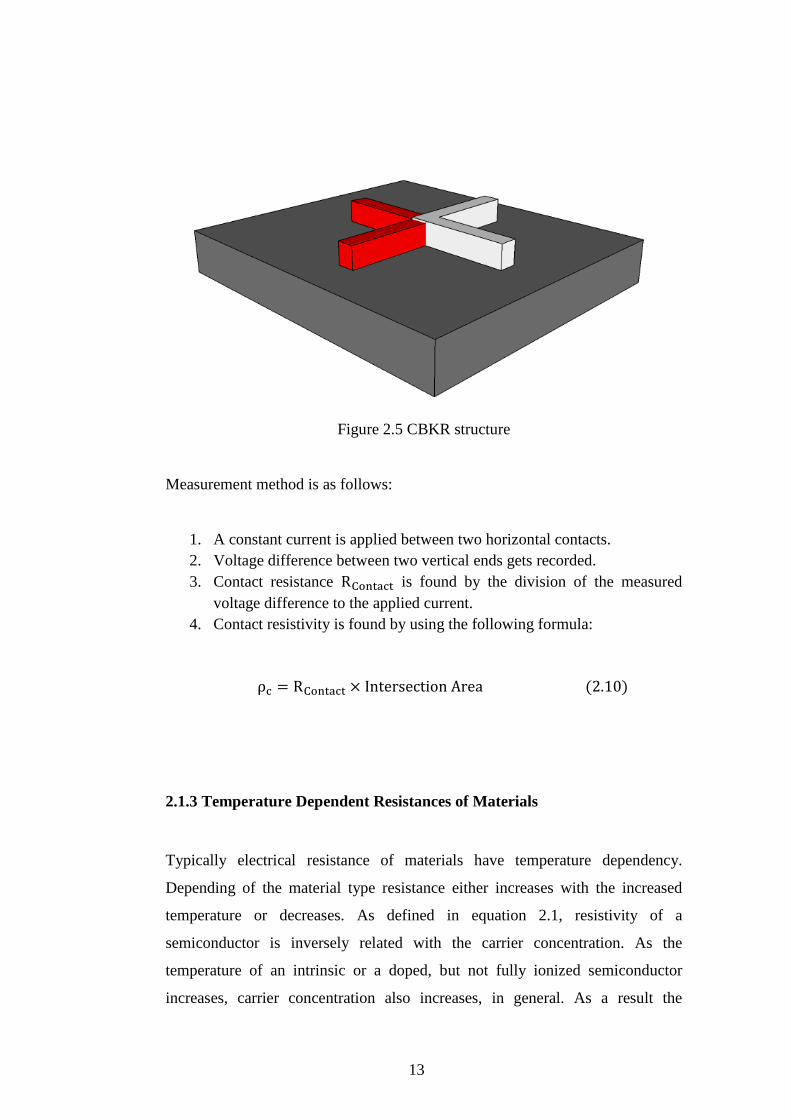
13
Figure 2.5 CBKR structure
Measurement method is as follows:
1. A constant current is applied between two horizontal contacts.
2. Voltage difference between two vertical ends gets recorded.
3. Contact resistance is found by the division of the measured
voltage difference to the applied current.
4. Contact resistivity is found by using the following formula:
( )
2.1.3 Temperature Dependent Resistances of Materials
Typically electrical resistance of materials have temperature dependency.
Depending of the material type resistance either increases with the increased
temperature or decreases. As defined in equation 2.1, resistivity of a
semiconductor is inversely related with the carrier concentration. As the
temperature of an intrinsic or a doped, but not fully ionized semiconductor
increases, carrier concentration also increases, in general. As a result the

14
resistivity decreases. Same case applies in insulators, however, since the
insulators do not have a considerable amount of carriers available for
conduction, the temperature dependency of the resistance is not expected to be
as impactful as it is in semiconductors. Metals, on the other hand, have the sea
of electrons in their conduction band and the increased temperature results in the
increased number of scattering of the carriers. As a result, resistivity of this
material type increases when the temperature is increased. The dependency of
the resistance to the temperature is given the special name of “temperature
coefficient of resistance” (TCR) and it can be calculated by the use of following
formula:
(2.11)
2.1.4 Electronic Noise in Resistors
There are mainly two types of electronic noise present in almost all electronic
devices, namely, thermal noise and flicker noise. Thermal noise is mainly
caused by the random motion of the charge carriers. Flicker noise, on the other
hand relates to the charge trap states present in the active device region and the
roughness of the material. Electric noise has several significant outcomes in the
operation of the devices. Some of these effects are:
1. Minimum signal that can be processed or detected is limited.
2. Noise level trades with the dissipated power. To reduce the noise, large
capacitance is commonly used in most of the circuits, thereby resulting
in the high power dissipation.
3. With the lowered operation voltages of the modern circuits, signal to
noise ratio dercreases while it increases the importance of the noise
present in the circuit.

15
Thermal noise is present in every electrical component and rises as a result of
DC conductance. Since the random collisions occur with the relaxation time
values in the order of pico seconds, it is currently not possible to obtain the
instantaneous value of the thermal noise. Only the avarage power of the thermal
noise can be obtained. A resistance can be modeled as a resistor connected in
parallel with a current source to take the effects of the thermal noise into
account.
Frequency dependency of the thermal noise power was shown by Nyquist and
formulated as:
(2.12)
The value Pn corresponds to the average noise power occuring in the specified
frequency range where the highest and the lowest frequency values are separated
by Δf amount. k is the Boltzmann’s constant and T is the absolute temperature
value.
Flicker noise, by definition, inversely depends on frequency. Following equation
shows the spectral flicker noise density.
⁄
(2.13)
K is the proportionality constant. “f2 and f1” are the boundaries of the specified
frequency region. The point in the frequency domain, at which the flicker noise
is equal to the thermal noise is known as the corner frequency. The value of the
corner frequency carries vital importance in the operation of the devices.

16
2.2 Metal Oxide Semiconductor Field Effect
Transistor (MOSFET) Basics
MOSFET is a type of transistor utilizing the electric field effect created within
the MOS structure for controlling the conductivity of the semiconducting
channel between the so called source and drain contacts. The metal contact of
the MOS structure is named as the gate terminal of the device. MOSFETs are
the most commonly used transistor types of the current digital and analog
electronics industry.
There are mainly two types of MOSFETs, namely, n-channel MOSFETs and p-
channel MOSFETs. N-channel MOSFETs employ electrons as the current
carriers, whereas the latter employ holes for current conduction.
2.2.1 Operation Principles of MOSFETs
An illustrative schematic of the crossectional view of an n-channel MOSFET is
shown in Figure 2.6.
Figure 2.6 Crossectional view of an n-channel MOSFET structure [38]

17
The channel width is denoted as W, and the channel length is denoted as L. The
device consists of the highly doped n-type source and drain regions, whereas the
channel region is p-type without any gate bias. As the gate bias increases, it
repels the holes from the oxide semiconductor interface and immobile ionized
acceptors remain in this region. A further increase in the gate voltage results in
the inversion of the carrier type and the electrons get accumulated in the channel
region. This operation region is known as the strong inversion region. The gate
voltage required to achieve this condition is named as the threshold voltage
(VTH). After reaching the strong inversion condition, channel also becomes n
type and gets ready to conduct current between source and drain ends.
Depending on the value of the VTH, there are two types of MOSFETs, namely
depletion mode transistor in which the device operates under 0V gate bias, and
the enhancement mode device in which a gate bias should be applied to turn on
the transistor. In the strong inversion region, the motion of the channel electrons
is mainly based on the drift. And the current flowing into the device is
calculated by the following formula:
( ) ( ) (2.12)
-Qn(y) denotes the inversion charge per unit area at a position y in the channel
region, and v (y) is the drift speed of the carriers in the channel that can be
calculated by:
( ) ( ) (2.13)
Where µn denotes the mobility of the carriers, and ε(y) denotes the electric field
created in the channel within the y directon. Electric field can be calculated as:
( ) ( )
(2.14)

18
Qn(y) can be calculated as follows:
( ) ( ) (2.15)
Where the COX represents the oxide capacitance. There are two assumptions
made for obtaining equation 2.15, which are (1) both the channel inversion and
bulk charges are influenced by the vertical field only and (2) VTH is not a
function of the position (y) along the channel. If the equations 2.13, 2.14 and
2.15 are inserted in equation 2.12 and when the integration is carried out along
the channel (between y=0 (V=0) and y=L (V=VD)) the current equation is
obtained as follows:
∫
∫ ( )
(2.16)
Finally the device current is obtained as:
[(
) ] (2.17)
Equation 2.17 governs the device current for the low VD values and the
dependence of the ID to VD is linear. As a result, this region of operation is
named as the linear region. As the VD increases the slope of the ID vs VD
decreases. After VD reaches the value of VG-VTH, channel becomes depleted of
the carriers at the drain end of the device, and this condition is known as the
pinch-off condition. After this value, ideally the increase in the drain voltage
does not cause any increase in the conductivity of the channel and thus the
current becomes constant without depending on the applied drain voltage. This
region of the operation is named as the saturation region, and the device current
can be calculated by inserting VD = VG-VTH in equation 2.17, and found to be:
( ) (2.18)

19
2.2.2 Subthreshold Region
Under ideal conditions, the MOSFET is expected to turn on and off immediately
at the threshold voltage level. However, the carriers in the channel generally
follow an exponential dependence for the gate bias levels lower than the
threshold voltage. This region of operation is known as the subthreshold region.
When the device current is plotted with respect to the changing gate voltage, the
linear shape is observed on the semilogaritmic curve in the subthreshold region.
The inverse slope of this line is defined as the subthreshold swing (SS) of the
transistor. Low SS is desired in transistors so that the total power consumption
becomes as low as possible. For a typical MOSFET SS can be calculated by
using the following formula:
(
)
(
)
(2.19)
2.3 Thin Film Transistors (TFTs)
TFT is a special type of MOSFET in which the substrate is typically an
insulating substrate rather than a semiconducting material. As opposed to the
classical MOSFET, substrate is just used to carry the device, rather than
participating in the channel formation. In TFTs, channel is formed in a thin
lowly doped active layer material. Depending on the positions of the gate and
the source/drain contacts there are mainly four different types of the thin film
transistor. Bottom gate staggered TFTs are fabricated and characterized in the
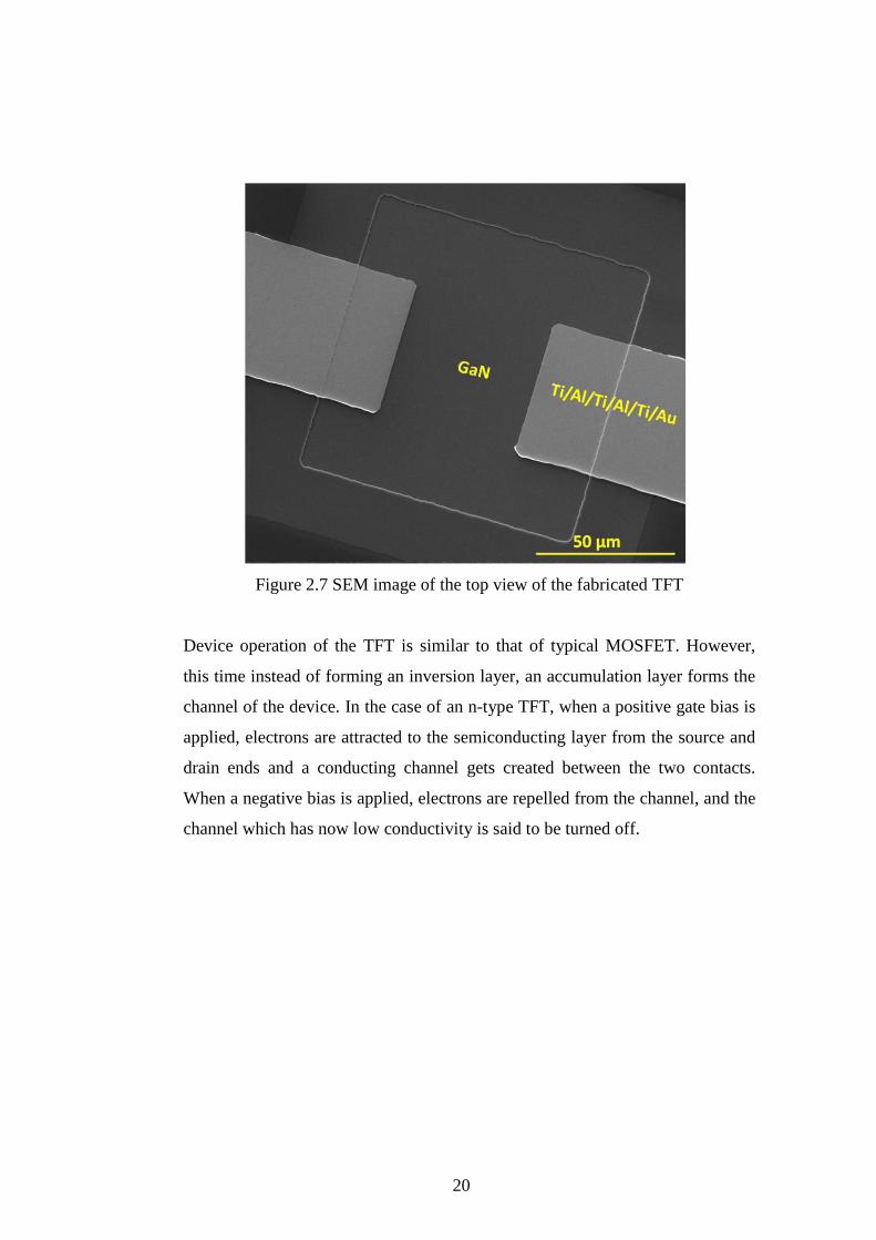
works of this thesis, SEM image of which is shown in Figure 2.7.
20
Figure 2.7 SEM image of the top view of the fabricated TFT
Device operation of the TFT is similar to that of typical MOSFET. However,
this time instead of forming an inversion layer, an accumulation layer forms the
channel of the device. In the case of an n-type TFT, when a positive gate bias is
applied, electrons are attracted to the semiconducting layer from the source and
drain ends and a conducting channel gets created between the two contacts.
When a negative bias is applied, electrons are repelled from the channel, and the
channel which has now low conductivity is said to be turned off.

21
Chapter 3
Experimental Methods
This chapter provides the experimental details of the works covered in this
thesis. The first part of the chapter includes the description of the fabrication
equipment, and the second part provides the fabrication details of the all of the
devices.
3.1 Fabrication Equipments
3.1.1 Plasma Enhanced Chemical Vapor Deposition (PECVD)
Top to bottom isolation of the fabricated devices of this thesis is achieved by the
plasma enhanced chemical vapor deposition of SiO2.
Plasma enhanced chemical vapor deposition is a widely utilized technique for
the low temperature deposition of the nitrides and oxides. In this technique, the
precursors are introduced to the chamber in their gas forms. Then, these gases
are ionized with the help of the RF power created in the reactor. After the

22
reaction occurs, the thin film gets coated on the surface of the substrate. The
quality of the coated film is enhanced due to the electric field created between
the substrate and the plasma source [39]. Figure 3.1 shows a PECVD reactor.
Figure 3.1 Vaksis Handy CVD/PECVD System
The main advantage of the PECVD over the classical CVD is that the plasma
enhancement reduces the temperature required for the reaction of the precursors.
The chemical reaction for obtaining SiO2 in PECVD system is as follows:
3SiH4 + 6N2O 3 SiO2 + 4NH3 + 4N2
3.1.2 Atomic Layer Deposition (ALD)
The semiconductor materials and insulating oxides of the devices included in
this thesis are fabricated by using atomic layer deposition technique.

23
ALD can be defined as a modified version of chemical vapor deposition, in
which the precursors are introduced to the surface at separate cycles. During
each cycle, saturation of the precursor on the surface occurs and this results in a
self-limiting growth. Main advantages of this mechanism are the accurate
thickness control, good uniformity and perfect conformity. [33]
There are mainly two types of ALD:
a) Thermal ALD
b) Plasma Enhanced (Assisted) ALD (PEALD or PA-ALD)
Depositions of the ZnO and Al2O3 thin films are performed by the utilization of
the thermal ALD technique. Figure 3.2 shows the thermal ALD reactor in which
the depositions are performed.
Figure 3.2 Cambridge NanoTech Savannah 100 Atomic Layer Deposition
System

24
Operation steps of the thermal ALD in a single cycle are as follows:
1. Introduction of the first precursor to the chamber (“i" in Figure 3.3)
2. Purge or evacuation of chamber (“ii” in Figure 3.3)
3. Introduction of the second precursor to the chamber (“iii” in Figure 3.3)
4. Purge or evacuation of chamber
After each cycle, an amount of the material is grown on the surface; the
specified thickness of this material is named as growth per cycle (GPC) [33]. In
most of the processes GPC does not depend on the number of the ALD cycles,
as a result the total thickness of the film can easily be calculated by multiplying
the GPC with how many times the ALD cycle is repeated. For a better
understanding, ALD growth of the ZnO is given in Figure 3.3.
Figure 3.3 Step by step demonstration of one ALD cycle of ZnO growth

25
Depositions of the GaN thin films, which are the active layer of the TFTs of this
study, are performed in a modified PEALD reactor, which is shown in Figure
3.4.
Figure 3.4 Cambridge NanoTech Fiji F200 PEALD reactor
The main difference between the PEALD and thermal ALD is that in PEALD
one of the precursors is the plasma ion combination of the specified gas(es). The
use of plasma comes with the advantage of reducing the deposition temperature.
However, in general, the duration of the deposition is longer in PEALD. Table
3.1 summarizes the ALD precursors used in this thesis.

26
Table 3.1 ALD precursors used for the deposition of ZnO and GaN thin films.
Element Precursor
Gallium Trimethylgallium Ga(CH3)3
Zinc Diethylzinc (C2H5)2Zn
Nitrogen N2/H2 plasma or NH3 pasma
Oxygen mili-Q water H2O
3.1.3 Thermal Evaporator
Contact metallizations of the structures having ZnO active layers are done by the
thermal evaporation of Al and Pd layers. Figure 3.5 shows the evaporation
reactor used in this thesis.
Figure 3.5 Vaksis MIDAS Thermal Evaporator PVD/3T

27
Thermal evaporation can be described as a physical vapor deposition technique,
in which the evaporation and the deposition of the desired film is achieved via
the resistive heating of an underlying conductive boat. The parameters used for
the Al and Pd depositions are summarized in table 3.2. The deposition rate is
adjusted instantly with the help of a crystal thickness monitor.
Table 3.2. Physical vapor deposition parameters of Aluminium and Palladium
layers.
Material Density(g/cm3) Acoustic
Resistance
Tooling Factor
Aluminium 2.8 8.17 85%
Palladium 12.02 24.73 60%
3.1.4 DC Magnetron Sputtering
Deposition of the source and drain contact metal stacks for the GaN based TFTs
of this thesis are performed via the DC magnetron sputtering system shown in
Figure 3.6.

28
Figure 3.6 Vaksis MIDAS Magnetron Sputtering PVD/4M
The main mechanism of a sputtering event can be described as follows:
energetic ions of the plasma created in the reactor with the help of the applied
DC power, collides with the surface atoms of the sputtering target, results in the
scattering of the surface atoms. As a result of the scattering, the energized
atoms, as well as the ions make several collisions with the sputtering target, and
the atoms sputtered from the target surface get coated to the substrate.
The metallization scheme formed by sputtering consists of the sequential
combination of Ti, Al and Au layers. The parameters used for the deposition of
these layers are given in Table 3.3.

29
Table 3.3. Sputtering parameters of Ti, Al, and Au
Material Plasma
Power
Pressure Ar flow rate Deposition
rate
Ti 125W 10mTorr 8sccm 10nm/min
Al 150W 20mTorr 20sccm 3nm/min
Au 75W 10mTorr 50sccm 25nm/min
3.1.5 Mask Aligner and Photolithography
Patterning steps of the all of the layers of the devices are performed by using
photolithography. There are basically two different photolithography methods
used in the works included in this thesis. First one is the patterning of the readily
formed layer, whereas the second one is the photolithography of a layer before it
gets formed. The steps followed in the lithography are as follows:
1. General cleaning of the substrate:
This step consists of the solvent cleaning for the removal of the possible organic
contamination of the substrate surface. Cleaning starts with the soaking of the
sample to the acetone, which is followed by the isopropanol application, then
finalized by the spraying DI water and the drying of the sample with the
nitrogen gas.
2. De-hydration step:
This step consists of the vaporization of the possible water drops on the
substrate surface. The sample gets placed on the surface of a hot plate, the
temperature of which is kept at 110°C, which is higher than the evaporation
temperature of the water.

30
3. Photoresist Coating:
After the vaporization step, photoresist can be coated on the substrate surface.
However, it is generally preferred to deposit a chemical called Bis
(trimethylsilyl) amine (HMDS) as an adhesion layer prior to photoresist
deposition. AZ514E is used as the photoresist in the studies of this thesis.
4. Pre-bake Step:
This step is done to drive off the excess photoresist solvent from the substrate
surface. The photoresist coated sample gets placed on a hot plate with 110°C
surface temperature for 60 seconds.
5. Exposure Step:
After the prebake of the photoresist coated sample, 40 mJ/cm2 of UV light
exposure is applied in the mask aligner shown in Figure 3.7. During this step,
some parts of the sample are protected from the UV light with the help of the
special masks.
31
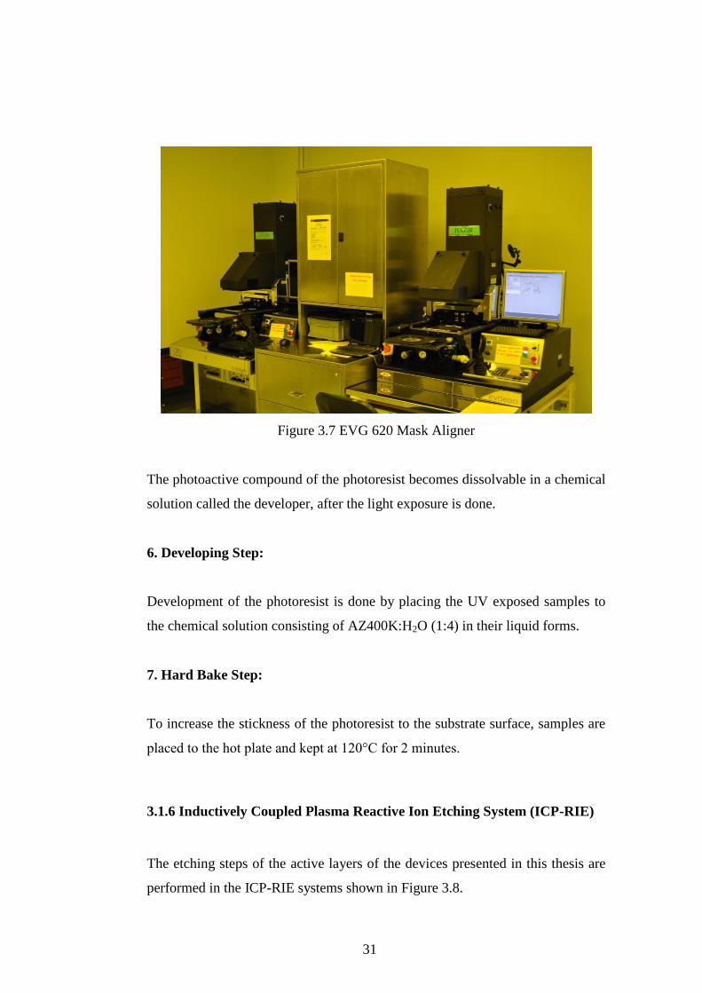
Figure 3.7 EVG 620 Mask Aligner
The photoactive compound of the photoresist becomes dissolvable in a chemical
solution called the developer, after the light exposure is done.
6. Developing Step:
Development of the photoresist is done by placing the UV exposed samples to
the chemical solution consisting of AZ400K:H2O (1:4) in their liquid forms.
7. Hard Bake Step:
To increase the stickness of the photoresist to the substrate surface, samples are
placed to the hot plate and kept at 120°C for 2 minutes.
3.1.6 Inductively Coupled Plasma Reactive Ion Etching System (ICP-RIE)
The etching steps of the active layers of the devices presented in this thesis are
performed in the ICP-RIE systems shown in Figure 3.8.

32
Figure 3.8 STS 615-616 ICP RIE Systems
The main operation of the dry etching is based on the chemical and physical
interaction of the layer to be etched with the etchant chemical gases. Use of the
plasma (highly directional ions) makes this etching technique a highly
anisotropic one. Table 3.4 shows the etching parameters of GaN and ZnO.
Table 3.4 Dry etch parameters of GaN and ZnO thin films
Material Etchant
Gas
Pressure Platen
Power
Coil
Power
Etch Rate
GaN Ar 10mTorr 100W 500W 20nm/minute
ZnO BCl3 10mTorr 100W 800W 50nm/minute

33
3.2 Device Fabrication Steps
3.2.1 Van Der Pauw Structures
Fabrication starts with the Radio Corporation of America (RCA) cleaning of the
thermal oxide coated Si (111) wafers. Next the deposition of the active layer is
performed in ALD reactors. These layers are patterned via standard
photolithography and dry etching. Contacts are formed via the physical vapor
deposition and lift-off of the specified metals for each active layer. Al is chosen
as the contact metal to ZnO, whereas Ti/Au stack is used as the contact layer of
the GaN based Van Der Pauw structures. Figure 3.9 shows the fabrication of
these structures in a stepwise manner.
Figure 3.9 Fabrication steps of Van Der Pauw structures

34
3.2.2 Cross Bridge Kelvin Resistors (CBKR)
Fabrication steps are same as the ones of the Van Der Pauw Structures. Figure
3.10 shows the step by step fabrication of the CBKR structures.
Figure 3.10 Fabrication steps of CBKR structures.

35
3.2.3 Thin Film Resistors with Interdigitated Contact Structures
Fabrication steps are same as the ones in 3.2.1. Figure 3.11 shows the
fabrication steps of this structure.
3.11 Fabrication steps of the resistors with interdigitated contact structures
3.2.4 Bottom Gate Thin Film Transistors (BG-TFTs)
3.2.4.1 Thin Film Transistors with NH3 Plasma Assisted Atomic Layer
Deposited GaN Channels
The TFT fabrication process begins with the standard RCA cleaning of low
resistivity p-type (1-5 mΩ-cm) Si substrate, which is also employed as the gate
terminal of the TFT. Next, a 200-nm-thick SiO2 layer is deposited by plasma-
enhanced chemical vapour deposition (PECVD) at 250 °C to achieve electrical
isolation between the source-drain contacts and the Si bottom gate. Then, active

36
device areas are patterned by optical lithography and wet etching of SiO2. This
is followed by the thermal and HCPA-ALD of Al2O3 and GaN (30nm/20nm)
gate stack at 200 °C, respectively. Afterwards, channel region is patterned via
optical lithography and dry etching of GaN thin films. Ti (20nm) /Au (80nm)
source and drain electrodes are sputtered and then patterned by the lift-off
technique. Finally, contact annealing is performed at 600 °C in N2 ambient for
30 s using a rapid thermal annealing system (RTA).
3.2.4.2 Thin Film Transistors with N2/H2 Plasma Assisted Atomic Layer
Deposited GaN Channels
Fabrication of the bottom gate TFT starts with the RCA cleaning of the highly
doped (1–5 mΩ-cm) p-type Si wafer. Plasma-enhanced chemical vapor
deposition of a 200–nm-thick SiO2 is performed at 250 °C. The SiO2 film is
patterned to define the active device areas. An HF-last clean is immediately
followed by the growth of 77-nm-thick Al2O3 and 11-nm-thick GaN
subsequently deposited at a single ALD process in a modified Fiji F200-LL
ALD Reactor (Ultratech/Cambridge NanoTech Inc.), where the process
temperature is kept at 200 °C. Active device areas are isolated by Ar-based dry
etching of the GaN layer. Source and drain contacts are formed by sputtering a
multilayer metal stack consisting of Ti/Al/Ti/Al/Ti/Au (30/30/30/30/30/60 nm)
as suggested in Ref.40. Figure 3.12 summarizes the fabrication steps of the BG-
TFTs.

37
Figure 3.12 Fabrication steps of the bottom gate thin film transistors
3.3 Electrical Characterization of the Devices
3.3.1 Semiconductor Parameter Analyzer (SPA)
A Keithley 4200 SPA is used for the resistivity and contact resistance
measurements of the thin films as well as for the output and transfer
characteristics measurements of the BG-TFTs. Figure 3.13 shows the
photograph of this characterization equipment.

38
Figure 3.13 Keithley 4200 Semiconductor Parameter Analyzer and Probe
Station
Resistivity measurement is performed on Van Der Pauw structures in the
following way:
1. A constant current is applied between two adjacent contacts
2. The voltage difference between the remaining contacts are measured.
The contact resistance measurement is done on CBKR structures in the
following way:
1. A constant current is applied between two horizontal ends
2. The voltage difference between the vertical ends is measured.
Output characteristics of the BG-TFTs are obtained as follows:
1. A constant gate bias is applied
2. The voltage difference between the drain and source contacts is swept
3. Step 2 is repeated under different gate bias conditions, and the so called
family of curves is obtained.

39
Transfer characteristics of the BG-TFTs are obtained by following the steps
given below:
1. A constant bias is applied between drain and source ends.
2. Gate voltage is swept to observe the current difference between on and off
states of the device.
3.3.2 Temperature Dependent Electrical Characterization Setup
TCR of the ZnO active layers is measured in the following way:
1. A constant current is applied between the two contact pads of the
interdigitated resistor structures.
2. The voltage difference between the two ends is measured
simultaneously.
3. The temperature is increased from 15 °C to 35 °C in a period of 30
minutes.
A photograph of the TCR measurement set-up is given in Figure 3.14.
Figure 3.14 TCR Measurement setup

40
Chapter 4
Electrical Properties of Atomic Layer
Deposition Based ZnO Thin Films
This chapter consists of the results and discussion of the studies which cover the
resistivity, contact resistance and temperature dependent electrical
characterization of the ALD grown ZnO thin films.
4.1 Contact resistance of the Metal/ZnO junctions
In order to form an ohmic contact to a semiconductor, a junction allowing the
current flow in both reverse and forward bias cases is required. ZnO is known to
have a band gap of 3.37 eV [1] and the reported electron affinity and work
function values for this compound are 4.29 eV and 4.45 eV [1] (changes with
the doping concentration). To form an ohmic contact to ZnO, either a tunneling
junction can be formed, which requires high doping levels at ZnO-metal
interface, or a metal with the work function lower than ZnO can be used as the
contact material.

41
To determine the suitable ohmic contact metal to ALD grown ZnO, contact
resistance study is conducted with two different metals, namely Al with a work
function of 4.3 eV and Pd with the work function of 5.1 eV. The main reason of
choosing these materials is to experimentally observe the effect of work function
in the electrical properties of the metal-ZnO junctions. Electrical
characterization is conducted on CBKR structures. An illustrative SEM image
from a CBKR structure fabricated in this study is shown in Figure 4.1.
Figure 4.1. SEM image of the CBKR structure
Electrical characterization is performed as described in theoretical background
section (see Section 2.1.2.2). Table 4.1 summarizes the obtained contact
resistance values with the 80°C ALD grown ZnO as the semiconductor; Al and
Pd as the metal layers. To understand the effect of the intersection area on the
contact properties, measurements are performed on structures with different
overlap areas.

42
Table 4.1. Contact Resistance measurement results (Al-ZnO &Pd-ZnO contacts)
Contact
Properties
Intersection Area Measured
Resistance
Contact
Resistivity
ZnO-Al 100µm2 5-25 Ω
Ωcm2
ZnO-Al 400µm2 1-5 Ω 4x10⁻⁶ -2x10⁻⁵
Ωcm2
ZnO-Al 2500µm2 <0.5 Ω <1.25x10⁻⁵Ωcm
2
ZnO-Pd 100µm2 2205 Ω 2.7x10⁻³ Ωcm
2
ZnO-Pd 400µm2 880 Ω 3.52x10⁻³Ωcm
2
ZnO-Pd 2500µm2 150 Ω 3.75x10⁻³Ωcm
2
As the first implication of the experimental results, the contact resistance values
of ZnO-Al junction are observed to be almost 3 orders of magnitude less than
that of ZnO-Pd contacts. This is expected because, due to the work function
differences, Al is expected to form an ohmic contact to ZnO whereas the contact
between ZnO and Pd is expected to be a Schottky one. Similar values for Al-
ZnO junctions are also available in the literature [1]. The contact resistance
values seem to show small variations with the change in the overlap area of the
metal semiconductor junction. This can be due to the current crowding. The
carriers of the electronic conduction always prefer the easiest path while flowing
in a region. However, the discrepancies between the resistance values of the
structures with the smallest and the largest intersection area are smaller than one
order of magnitude, making this problem somewhat ignorable. Normally, to
solve the current crowding problem, spherical contacts rather than rectangular
ones are preferred. This is done to eliminate the effect of sharp edges on current
crowding. In the end, the results show that Al can be used as an ohmic contact
material to ALD grown ZnO.

43
4.2. Resistivity of the Atomic Layer Deposited
ZnO
As also described in theoretical background section, Van Der Pauw structures
are designed and fabricated for obtaining the sheet resistance of the ALD grown
ZnO thin films. An illustrative SEM image of the fabricated structure is shown
in Figure 4.2.
Figure 4.2 SEM image of the Van Der Pauw Structure
After obtaining good quality ohmic contacts to ZnO by using Al as the contact
metal, this material has been used as the metal contact of the resistivity
measurement structures. In order to observe the effect of the deposition
temperature on the electrical properties of the ZnO thin films, film depositions

44
are performed at four different temperature levels, namely 80°C, 120°C, 200°C
and 250°C with the growth recipes given in experimental section (see Section
3.1.2) Electrical characterization of the structures are conducted as described in
experimental section (see Section 3.3.1) and the corresponding resistivity values
are obtained as explained in the theoretical background section (see Section
2.1.1.2). Table 4.2 shows the measured resistivities of the ZnO thin films grown
at different temperature levels.
Table 4.2. Resistivity of the ZnO films grown at 80, 120, 200 and 250°C
temperature levels.
Growth
Temperature
Resistivity of the thin film
80°C Ω-cm
120°C Ω-cm
200°C Ω-cm
250°C Ω-cm
Increasing deposition temperature results in higher free-carrier concentrations,
therefore, lower resistivity values. This behavior is in agreement with earlier
reports on ZnO deposited by ALD and sputtering in similar deposition
temperature ranges [41]. ZnO films exhibit n-type behavior, where n-type
conductivity is generally attributed to the existence of the zinc interstitials, and
oxygen vacancies [42]. The decrease of resistance with increasing deposition
temperature indicates that the ZnO grown at higher temperatures has a Zn-rich
composition, whereas the ZnO films grown at lower temperature levels are
oxygen-rich, as previously reported [42]. For the films grown at 80°C and
120°C, obtained values are not constant but changing during each measurement,
between the values noted in Table 4.2. This indicates that the films grown at
these temperatures have somewhat of stability issues.

45
As a result, it is shown that the electrical characteristics of the ALD based ZnO
thin films strongly depends on the growth temperature. The resistivity of the
films are obtained to be tunable up to 6 orders of magnitude, within the
deposition temperature range between 80°C and 250°C.
4.3 Temperature Dependent Electrical
characteristics of ALD grown ZnO
4.3.1 Temperature Coefficient of Resistance (TCR)
To measure the temperature dependent electrical characteristics of the ZnO thin
films, resistors with interdigitated contact structures are fabricated as described
in experimental section (see Section 3.2.3). SEM image of a such resistor is
given in Figure 4.3.
Figure 4.3 SEM image of a thin film resistor having interdigitated contact
structure

46
TCR of the ALD based ZnO thin films grown at 120, 200 and 250 °C are
obtained with the methods described in the experimental section (see section
3.3.2)
Figure 4.4 shows the temperature dependent resistance and Figure 4.5 shows the
temperature dependent TCR characteristics of the ZnO thin films grown at
120°C.
Figure 4.4 Temperature dependent resistance characteristics of 120°C grown
ZnO thin film.
47
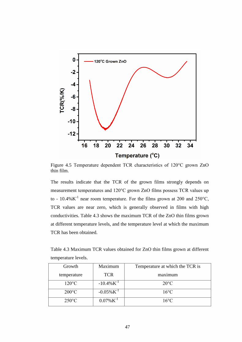
Figure 4.5 Temperature dependent TCR characteristics of 120°C grown ZnO
thin film.
The results indicate that the TCR of the grown films strongly depends on
measurement temperatures and 120°C grown ZnO films possess TCR values up
to - 10.4%K-1
near room temperature. For the films grown at 200 and 250°C,
TCR values are near zero, which is generally observed in films with high
conductivities. Table 4.3 shows the maximum TCR of the ZnO thin films grown
at different temperature levels, and the temperature level at which the maximum
TCR has been obtained.
Table 4.3 Maximum TCR values obtained for ZnO thin films grown at different
temperature levels.
Growth
temperature
Maximum
TCR
Temperature at which the TCR is
maximum
120°C -10.4%K-1
20°C
200°C -0.05%K-1
16°C
250°C 0.07%K-1
16°C

48
The TCR of ZnO thin film grown at 250°C is positive, whereas the TCR values
of the films grown at lower temperatures are negative. This suggests that the
behavior of a 250°C grown film is similar to that of a conductor, whereas the
ZnO thin films grown at lower temperatures have the typical behavior of
semiconductor materials. This is consistent with the measured resistivity values
of ALD-grown ZnO films. The resistivity measurement results also support the
change of sign (from negative to positive) in measured TCR values of ZnO
grown at higher temperatures, suggesting that ZnO deposited at 250°C behaves
as a decent conductor, but a semiconductor when deposited at 120°C.
4.3.2 Flicker Noise
Active layers with low electrical noise are sought in order to achieve high
sensitivity and detectivity in micro-bolometers. Important components of the
electrical noise in microbolometers are mainly flicker noise and thermal noise.
The spectral noise analyses of the ZnO thin films are performed on resistors
patterned on such films. Figure 4.7 shows the noise power spectral densities
(NPSD) of the thin film ZnO resistors grown at 120, 200, and 250°C.

49
Figure 4.6 NPSD characteristics of (a)120°C, (b) 200 and 250°C grown ZnO
thin films
The logarithmic NPSD–frequency plot indicates that the flicker noise is the
dominant mechanism in the 200 and 250°C grown ZnO thin films within the
measured frequency range (0–10 kHz). The corner frequency of 120°C grown
ZnO is at about 2 kHz, which falls in the suitable range for the bolometers
operating in snapshot mode [43]. The obtained results suggest that the ZnO thin
film grown at 120°C with the ALD method, in terms of electrical properties, is a
very promising candidate to be used as the active layer of uncooled
microbolometers.

50
Chapter 5
Electrical Properties and Device
Applications of Hollow Cathode
Plasma Assisted Atomic Layer
Deposition (HCPA-ALD) Based GaN
Thin Films
This chapter presents the electrical properties and the TFT applications of the
HCPA-ALD based GaN. Electrical properties, such as resistivity and contact
resistance of the GaN with Ti/Au metal stack are discussed and the effect of
post-metallization annealing on these properties are investigated. This part is
followed by the electrical characterization results of the HCPA-ALD based GaN
containing TFTs, which are reported for the first time in the literature [44].
Finally, the discussion of the electrical characteristics of the GaN transistor [45]
with the lowest process temperature up to date is given.

51
5.1 NH3 Plasma Assisted Atomic Layer Deposited
GaN Thin Films
Previous studies on GaN related device applications have generally focused on
sputtered layers. Moreover, TFTs with good electrical performance have been
reported with sputtered GaN channels [53,54]. In ref 53, sputtering is performed
at room temperature followed by contact annealing. The authors explain that the
annealing was performed by a three-step process (room temperature to 400 °C,
650 °C and 850 °C) to eliminate the cracking problem of the thin films. In their
following study (ref 54), the authors choose to sputter the GaN film at a
temperature of 550 °C. At this temperature, a wurtzite crystal structure was
obtained. Moreover, a 55-minute 500 °C contact anneal was used.
GaN thin films of this part are grown by HCPA-ALD at a low deposition
temperature of 200°C with the GaMe3 as the Ga precursor and the NH3 plasma
as the nitrogen precursor. Such grown films are shown to be polycristalline with
the crystallite size of 10.2 nm [33]. Elemental composition as a function of
depth is determined by XPS measurements, which revealed 42.19 at.% Ga,
55.18 at.% N, 1.51 at.% O, and 1.13 at.% Ar in the deposited GaN thin film after
60 s of in situ Ar ion etching. These results, at first glance, seem to show a
nitrogen-rich composition for the as-deposited thin film. However, it should be
noticed that nitrogen concentration is overestimated due to the contribution of
Auger Ga peaks that overlap with the N 1s peak in the XPS spectrum [33]

52
5.1.1 Electrical Properties
Resistivity measurements are conducted on Van Der Pauw structures and the
contact resistance measurements are conducted on CBKR structures. In order to
form ohmic contact to n type GaN, there are several metallization schemes
reported in literatüre [46]. However, most of them have the Ti as the interfacial
layer to obtain a high quality junction with the semiconductor layer. The main
reason of starting with Ti is to form the TiN buffer layer during the post-anneal
step. TiN is known to have a work function suitable to form an ohmic contact to
n-type GaN [46]. Ti/Au metal stack is used as the contact to the fabricated
structures. Au is chosen as the cap layer protecting the underlying Ti layer from
air exposure, which otherwise results in the formation of the TiO2, a
semiconducting material. Table 5.1 summarizes the measurement results.
Table 5.1 Resistivity of GaN thin films and the contact resistance between GaN
and Ti/Au metallization scheme after annealing at different temperatures.
Annealing details Resistivity
(Ω-cm)
Contact resistivity
(Ω-cm2)
As-deposited 475.7 4.124
400°C, 30 s 423.2 3.258
600°C, 30 s 410.4 3.243
800°C, 30 s 9.6 0.001
There is a slight decrease in the resistivity of GaN thin films with increasing
annealing temperature up to 800 °C, which can be attributed to the hydrogen
releasing. After annealing at 800 °C, however, resistivity of the film
significantly drops down to 9.6 Ω-cm. Moreover, the contact resistance between
GaN and Ti/Au stack is reduced significantly to 10-3
Ω-cm2. However, the film

53
surface is severely deformed after this high temperature annealing step, forming
blisters. This morphological change may have several reasons such as the
hydrogen impurity concentration in the deposited GaN thin film, and thermal
expansion mismatch between the different layers. However, the main reason is
blistering due to this high hydrogen concentration which is proven by the
secondary ion mass spectroscopy (SIMS) results [33]. Hydrogen, with a rapid
increase in the temperature, is known to cause blistering in annealed films
beyond a critical temperature [47-49]. Elemental hydrogen, if incorporated into
GaN thin films, is also known to passivate crystal imperfections such as
dangling bonds and vacancies. Owing to this property, H-atoms electrically
compensate the defect-related charge carrier concentration in the deposited
material [50]. Upon annealing at high temperatures (such as 800 °C) pockets of
molecular hydrogen form blisters in the film and hydrogen gas is released via
these micro cracks. Due to reduced hydrogen concentration, defect-related
charge carrier density in such films is increased. This is supported by the
significantly lower resistivity of the films after annealing at 800 °C for 30 s. As
a result, it is shown that the best contact to HCPA-ALD based GaN thin film
without causing surface deformation can be obtained after the annealing at 600
°C.
5.1.2 Bottom Gate Thin Film Transistors with NH3 Plasma Assisted Atomic
Layer Deposited GaN Thin Films
After obtaining the electrical properties of the GaN thin films, initial
demonstration of the TFT with the HCPA-ALD based such films is performed.
In order to reduce the resistivity of the thin films as well as to minimize their
contact resistance with Ti/Au layers without deforming the GaN surface, contact
annealing of the TFTs are performed at 600 °C, for 30 s in N2 ambient.

54
Figure 5.1. Transfer characteristics of the TFTs with NH3 plasma assisted ALD
based GaN channels
Transfer characteristics of the TFT with bottom-gate configuration and W/L of
50µm/50µm are obtained by sweeping the gate to source voltage (VGS) from 7 to
12V, while the drain to source voltage (VDS) is kept at 1V. As shown in Figure
5.1, the device has an ION/IOFF ratio of 4.7×10², and a sub-threshold swing of
1.5V/dec. Extracted threshold voltage from IDS vs VGS (red curve) graph is 8.2V.
The reason for having relatively low on-to-off ratio can be attributed to the high
resistivity of the deposited GaN thin films.

55
Figure 5.2. Output characteristics of the TFTs employing NH3 plasma assisted
ALD based GaN as the channel material.
Field effect mobility of the device in the linear operation region is found to be
8×10⁻³
cm2/V-sec. Low carrier mobility could be related to the trap states at the
semiconductor-insulator interface and the nanocrystalline defect-rich nature of
the deposited GaN thin films. Output characteristics of the same device are
shown in Figure 5.2 to exhibit traditional n-type enhancement mode field effect
transistor behavior, having clear pinch-off and saturation characteristics. Gate
control is also clear with the fact that increased gate voltage results in increased
drain current without damaging the saturating behavior of the device current
with increased drain voltage.
There are mainly two issues with the presented device that needs to be
improved, namely, low on-to-off ratio and the high gate leakage present between
the gate and drain/source region.

56
5.2 Bottom Gate Thin Film Transistors with N2/H2
Plasma Assisted Atomic Layer Deposited GaN
Thin Films
In the remaining study conducted with HCPA ALD based GaN thin film, N2/H2
plasma is used as the N2 precursor. Structural analysis of the thin film reveals
the polycrystalline nature of the deposited GaN thin film. The average crystallite
size of the polycrystalline wurtzite GaN film is found to be 9.3 nm [33].
Chemical composition of the GaN thin film is obtained by making use of XPS
with depth profile analysis, and 42.24 at.% Ga, 54.57 at.% N, 1.65 at. % O, 1.54
at.% Ar are detected in the film after 60 s of Ar ion etching. Overestimation of
the N content is observed due to the contribution of the Ga Auger peaks, which
overlap with the N 1s peak [33].
TFTs with the N2/H2 plasma assisted atomic layer deposition based GaN
channel layers are fabricated. As also explained in the experimental section, all
fabrication steps are performed with the temperature levels lower than 250 °C. A
schematic illustration of this device is given in Figure 5.3.
Figure 5.3 Schematic illustration of the TFT with N2/H2 plasma assisted ALD
based GaN channel layer.

57
Output electrical characteristics of the HCPA-ALD-based GaN TFTs are shown
in Figure 5.4.
Figure 5.4. Output Characteristics of the HCPA-ALD (N2/H2 plasma) based
GaN TFTs.
Fabricated devices have clear pinch-off and saturation characteristics, and they
exhibit n-type field effect transistor behavior. Transfer characteristics of the
devices with VDS = 1 V applied are shown in Figure 5.5.

58
Figure 5.5. Transfer Characteristics of the HCPA-ALD (N2/H2 plasma) based
GaN TFTs.
Fabricated TFT has an ION/IOFF ratio of 2x10³. The advantage of using a thick
gate insulator (77nm thick Al2O3) is that the gate leakage current was kept
below 0.5 pA for all the bias conditions. The threshold voltage of the device is
extracted from the transfer characteristics (using
IDS ) and it is found to be
11.8 V. Sub-threshold swing (SS) of the device is generally influenced by trap
states located in the forbidden gap. Extracted SS of the fabricated device is 3.3
V/decade. Charge mobility in the channel is extracted in the linear region of the
device operation (VGS = 20V and VDS = 1V) by using the equation given in (5.1),
where Cox is the gate oxide capacitance per unit area. Relative permittivity of the
ALD based Al2O3, required to calculate Cox, is obtained from a previous study
[51]. Calculated effective charge mobility in the channel is 0.025cm2/V-sec.
This particularly low mobility can be attributed to the nanocrystalline structure
of the HCPA-ALD based GaN thin films, and the surface states at the
semiconductor insulator interface.

59
(( )
)
(5.1)
Figure 5.6. Threshold shift vs. positive gate bias stress (2.5 MV/cm)
To further analyze the effect of trapped charges in the operation of the devices,
effect of the positive gate bias stress on the threshold voltage is investigated and
the results are shown in Figure 5.6. Prior to each stress cycle, devices are
characterized by acquiring their transfer curves. A 2.5MV/cm field is applied
between the gate and source/drain of the TFTs while both drain and the source
are kept at 0V. Following the stress cycle, the transfer characteristics of the
devices are obtained again. The difference in the threshold voltages between
these measurements is recorded as the threshold voltage shift. Threshold voltage
shift reveals the presence of charge trap states at the insulator semiconductor
interface and or within the Al2O3 dielectric layer. As seen in Figure 5.6,
threshold voltage shifts to higher values with longer applied positive gate bias
stress. This is due to increased number of trapped electrons which screen the

60
applied gate field resulting in an increased threshold voltage. However, the
increase in the threshold voltage after 1000s of bias stress is smaller than that of
high performance TFTs based on ZnO channels [52].
The main advantage of the present TFT over the one discussed in section 5.1.2 is
that, since the former has a thicker dielectric, the gate leakage is kept in the
range of femto amperes, which is far below the on current of the device. Another
advantage, which is also believed to pave the way for the flexible, transparent
GaN based electronics is that, in the fabrication of N2/H2 PA-ALD based GaN
TFTs, the processing temperature is kept below 250 °C, during all of the steps.
This is the lowest reported thermal budget for the GaN based transistors, so far.
61
Chapter 6
Conclusion
ZnO is an exciting material which has gained researchers’ attention to be used in
several applications including UV LEDs, lasers, photodetectors and TFTs.
Although having been investigated intensely, the infrared imaging applications
of this material are yet to be explored.
In the ZnO related parts of this thesis, the electrical properties of the ALD
grown ZnO and their temperature dependencies are studied. Van Der pauw
structures are used for the resistivity measurements, whereas the CBKR
structures are preferred for the determination of the contact resistances between
several metals and ALD based ZnO thin films.
In conclusion, the TCR and electrical noise together with the resistivity and the
contact properties of the ALD-grown ZnO are investigated for the first time for
its usage in uncooled microbolometers. Depositions are performed at various
temperatures to observe the effect of the growth temperature on the properties of
the ZnO. In terms of electrical properties, a tendency of becoming more
conductive with the increase in the deposition temperature has been observed

62
and it is related to the defect-rich structure of the deposited thin film. Owing to
several advantageous properties obtained by only changing the deposition
temperature, ALD-grown ZnO is shown to have a great potential for its usage in
uncooled microbolometers. 120 °C grown ZnO with the TCR of −10.4% K−1
and
flicker noise corner frequency of 2 kHz is demonstrated to be a promising
candidate on replacing the currently used active layer materials of commercial
microbolometers.
Although, ZnO rises up as a promising candidate in thermal imaging
applications, stability problem of the ZnO is the major obstacle in the way of
commercialization of ZnO based devices. To solve this problem, the alloying of
ZnO with some metals such as Al, Hf, In and Ga should be implemented. In
order to employ these alloys in flexible electronics, the atomic layer deposition
technique can be used. To improve the quality of the thin films, it might be even
better to use the plasma enhanced version of the atomic layer deposition. After
observing the stable electrical characteristics of the ternary alloys in the form of
XZO, or quaternary alloys in the form of XYZO, a bolometer employing such
materials can be designed and fabricated. The ultimate aim of this work can then
be achieved by replacing the currently used bolometer materials.
GaN is known as a transparent compound semiconductor with a bandgap of 3.4
eV. Due to its remarkable optical and electrical properties, intensive research
focused on this material and its applications during the last two decades. Among
other attractive material properties, high electron saturation velocity and wide
bandgap made GaN a strong candidate as the material of choice for high-
frequency and high-power electronics. In the device applications of GaN, high
temperature deposition techniques, such as MOCVD and MBE step up as the
most commonly used growth methods of this material. To introduce this
material to the low temperature applications regime, hollow cathode plasma
assisted atomic layer deposition (HCPA-ALD) technique is utilized. Although
the growth is successfully demonstrated by this method, the electrical properties

63
and the device applications of the HCPA-ALD based GaN thin films are still
unknown.
In the GaN related parts of this thesis, electrical properties of the GaN thin films
deposited by HCPA-ALD technique are studied, and the effect of contact
annealing on the resistivity of thin film and its contact resistance with Ti/Au
contacts is presented. The resistivity of the thin film is shown to range between
9.6 and 476 Ω-cm as a result of annealing at different temperatures, whereas the
contact resistance between GaN and Ti/Au metallization scheme is observed to
range between 4.124 Ω-cm2 and 10
-3 Ω-cm
2. A TFT with HCPA-ALD-grown
GaN channel is demonstrated for the first time, and the fabricated device is
shown to exhibit field effect transistor behavior, having clear pinch-off and
saturation characteristics. Designed device has an on-to-off ratio of 4.7×10², and
the sub-threshold swing is observed to be 1.5 V/dec.
After the demonstration of the first TFT with HCPA-ALD grown GaN channels,
GaN TFTs, with the lowest thermal budget to date, are fabricated with the
utilization of the same method. Deposited GaN thin film is shown to have a
polycrystalline wurtzite structure with a crystallite size of 9.3 nm. Elemental
analysis of the films reveals the low amount of oxygen in HCPA-ALD based
GaN thin films. Output characteristics of the TFTs are obtained which show that
the fabricated devices exhibit n-type enhancement mode field effect transistor
behavior with clear pinch-off and saturation characteristics. Transfer
characteristics of the devices show that the fabricated transistors have on-to-off
ratios of 2 × 10³. Finally, the effect of the positive gate bias stress on threshold
voltage of the devices is studied, and reasonable threshold voltage shifts for a
device with a considerably thick gate insulator are obtained. This study
demonstrates the possibility of using low-temperature ALD-grown GaN layers
for alternative and stable, flexible/transparent TFT devices upon further
materials and process optimization.

64
In the following works of the HCPA-GaN based device studies, TFTs on
flexible substrates can be studied. In addition, the substrate dependent growth of
the GaN thin films should be investigated for obtaining thin films with better
crystallinity. Furthermore, doping of this material at low temperatures should be
studied for achieving devices with high performances. Finally, low temperature
growth of the ternary alloys of the III-Nitride thin films and their device
applications should be studied.
65
Bibliography
[1] Brillson, Leonard J., and Yicheng Lu. "ZnO Schottky barriers and Ohmic
contacts." Journal of Applied Physics 109.12 (2011): 121301.
[2] Look, David C. "Recent advances in ZnO materials and
devices." Materials Science and Engineering: B 80.1 (2001): 383-387.
[3] Chen, Yefan, Darren Bagnall, and Takafumi Yao. "ZnO as a novel
photonic material for the UV region." Materials Science and
Engineering: B 75.2 (2000): 190-198.
[4] Yamada, Akira, Baosheng Sang, and Makoto Konagai. "Atomic layer
deposition of ZnO transparent conducting oxides." Applied Surface
Science 112 (1997): 216-222.
[5] Street, Robert A. "Thin‐Film Transistors." Advanced Materials 21.20
(2009): 2007-2022.
[6] Street, Robert A., ed. Technology and applications of amorphous silicon.
Vol. 37. Springer, 2000.
[7] Özgür, Ü., et al. "A comprehensive review of ZnO materials and
devices." Journal of Applied Physics 98.4 (2005): 041301.
[8] Fortunato, Elvira MC, et al. "Fully Transparent ZnO Thin‐Film
Transistor Produced at Room Temperature." Advanced Materials 17 5
(2005): 590-594.
[9] Hoffman, R. L., Benjamin J. Norris, and J. F. Wager. "ZnO-based
transparent thin-film transistors." Applied Physics Letters 82 5 (2003):
733-735.
[10] Carcia, P. F., et al. "Transparent ZnO thin-film transistor fabricated by rf
magnetron sputtering." Applied Physics Letters 82 7 (2003): 1117-1119.
[11] Sun, X. W., and H. S. Kwok. "Optical properties of epitaxially grown
zinc oxide films on sapphire by pulsed laser deposition." Journal of
Applied Physics 86.1 (1999): 408-411.

66
[12] Liu, Ying, et al. "Ultraviolet detectors based on epitaxial ZnO films
grown by MOCVD." Journal of Electronic Materials 29.1 (2000): 69-74.
[13] Tsurumi, Takaaki, et al. "Electric properties of zinc oxide epitaxial films
grown by ion-beam sputtering with oxygen-radical irradiation." Japanese
Journal of Applied Physics 38.6R (1999): 3682.
[14] Oruç, Feyza B., et al. "Thin-film ZnO charge-trapping memory cell
grown in a single ALD step." Electron Device Letters, IEEE 33.12
(2012): 1714-1716.
[15] Rogalski, Antoni. "Infrared detectors: an overview." Infrared Physics &
Technology 43.3 (2002): 187-210.
[16] Chen, Changhong, et al. "Linear uncooled microbolometer array based
on VOx thin films." Infrared Physics & Technology 42.2 (2001): 87-90.
[17] Mottin, Eric, et al. "Enhanced amorphous silicon technology for 320 x
240 microbolometer arrays with a pitch of 35 μm." Aerospace/Defense
Sensing, Simulation, and Controls. International Society for Optics and
Photonics, 2001.
[18] Ningyi, Y., et al. "Comparison of VO2 thin films prepared by inorganic
sol-gel and IBED methods." Applied Physics A 78.5 (2004): 777-780.
[19] Xiao-Fang, Zhou, et al. "Giant Temperature Coefficient of Resistance in
ZnO/Si (111) Thin Films." Chinese Physics Letters 27.1 (2010): 018101.
[20] Zhou, X. F., et al. "Giant temperature coefficient of resistance in Co-
doped ZnO thin films." Applied Physics A 114.3 (2014): 809-812.
[21] Bingce, Liu, et al. "Temperature coefficients of grain boundary resistance
variations in a ZnO/p-Si heterojunction." Journal of
Semiconductors 31.12 (2010): 122001.
[22] He, Guan-nan, Bo Huang, and Hui Shen. "Positive temperature
coefficient of resistance of single ZnO nanorods." Nanotechnology 22.6
(2011): 065304.
[23] Leskelä, Markku, and Mikko Ritala. "Atomic layer deposition (ALD):
from precursors to thin film structures." Thin Solid Films 409.1 (2002):
138-146.

67
[24] Mishra, Umesh K., Primit Parikh, and Yi-Feng Wu. "AlGaN/GaN
HEMTs-an overview of device operation and applications." Proceedings,
IEEE 90.6 (2002): 1022-1031.
[25] Sheu, Jinn-Kong, et al. "White-light emission from near UV InGaN-GaN
LED chip precoated with blue/green/red phosphors." Photonics
Technology Letters, IEEE 15.1 (2003): 18-20.
[26] Pearton, S. J., et al. "GaN-based diodes and transistors for chemical, gas,
biological and pressure sensing." Journal of Physics: Condensed
Matter 16.29 (2004): R961.
[27] Walker, D., et al. "High-speed, low-noise metal–semiconductor–metal
ultraviolet photodetectors based on GaN." Applied Physics Letters 74.5
(1999): 762-764.
[28] Joshin K., et al. presented at the Electron Devices Meeting, 2003. IEDM
'03 Technical Digest. IEEE International, 2003
[29] Nakamura, Shuji, Yasuhiro Harada, and Masayuki Seno. "Novel
metalorganic chemical vapor deposition system for GaN
growth." Applied Physics Letters 58.18 (1991): 2021-2023.
[30] Tarsa, E. J., et al. "Homoepitaxial growth of GaN under Ga-stable and N-
stable conditions by plasma-assisted molecular beam epitaxy." Journal of
Applied Physics 82.11 (1997): 5472-5479.
[31] Chen, Rongsheng, Wei Zhou, and Hoi Sing Kwok. "Top-gate thin-film
transistors based on GaN channel layer." Applied Physics Letters 100.2
(2012): 022111.
[32] Kobayashi, Atsushi, et al. "Room temperature epitaxial growth of m-
plane GaN on lattice-matched ZnO substrates." Applied Physics
Letters 90.4 (2007): 041908-041908.
[33] Ozgit-Akgun, Cagla, et al. "Hollow cathode plasma-assisted atomic layer
deposition of crystalline AlN, GaN and Al x Ga1− x N thin films at low
temperatures." Journal of Materials Chemistry C 2.12 (2014): 2123-
2136.

68
[34] International Technology Roadmap for Semiconductors, Semiconductor
Industry Assoc., (2011).
[35] Chen, Rongsheng, et al. "Bottom-gate thin-film transistors based on GaN
active channel layer." Electron Device Letters, IEEE 34.4 (2013): 517-
519.
[36] Liu, Cheng, et al. "Plasma-Enhanced Atomic Layer Deposition of AlN
Epitaxial Thin Film for AlN/GaN Heterostructure TFTs." Electron
Device Letters, IEEE 34.9 (2013): 1106-1108.
[37] http://web.tiscali.it
[38] http://www.ece.nus.edu.sg
[39] Adamik, John A., et al. "Thermal CVD/PECVD reactor and use for
thermal chemical vapor deposition of silicon dioxide and in-situ multi-
step planarized process." U.S. Patent No. 5,000,113. Mar. 19 1991.
[40] Pang, Liang, and Kyekyoon Kim. "Improvement of Ohmic contacts to n-
type GaN using a Ti/Al multi-layered contact scheme." Materials
Science in Semiconductor Processing (2013).
[41] Lim, S. J., Soonju Kwon, and H. Kim. "ZnO thin films prepared by
atomic layer deposition and rf sputtering as an active layer for thin film
transistor." Thin Solid Films 516.7 (2008): 1523-1528.
[42] Guziewicz, E., et al. "ALD grown zinc oxide with controllable electrical
properties." Semiconductor Science and Technology 27.7 (2012):
074011.
[43] Rogalski, A. "Optical detectors for focal plane arrays." Optoelectronics
Review 12.2 (2004): 221-245.
[44] Bolat, S., et al. “Thin film transistors with GaN channels grown by
hollow cathode plasma-assisted atomic layer deposition”, Journal of
Vacuum Science and Technology A (submitted)
[45] Bolat, S., et al. "Low temperature thin film transistors with hollow
cathode plasma-assisted atomic layer deposition based GaN
channels." Applied Physics Letters 104.24 (2014): 243505.

69
[46] Fan, Zhifang, et al. "Very low resistance multilayer Ohmic contact to
n‐GaN."Applied Physics Letters 68.12 (1996): 1672-1674.
[47] Kucheyev, S. O., et al. "Blistering of H-implanted GaN." Journal of
Applied Physics 91.6 (2002): 3928-3930.
[48] Bedell, Stephen W., and William A. Lanford. "Investigation of surface
blistering of hydrogen implanted crystals." Journal of Applied
Physics 90.3 (2001): 1138-1146.
[49] Bruel, Michel, Bernard Aspar, and Andre-Jacques Auberton-Herve.
"Smart-Cut: a new silicon on insulator material technology based on
hydrogen implantation and wafer bonding." Japanese Journal of Applied
Physics 36.3S (1997): 1636.
[50] Pearton, S. J., et al. "Effects of hydrogen implantation into
GaN." Nuclear Instruments and Methods in Physics Research Section B:
Beam Interactions with Materials and Atoms 147.1 (1999): 171-174.
[51] Groner, M. D., et al. "Low-temperature Al2O3 atomic layer deposition."
Chemistry of Materials 16.4 (2004): 639-645.
[52] Cross, R. B. M., and M. M. De Souza. "Investigating the stability of zinc
oxide thin film transistors." Applied Physics Letters 89.26 (2006):
263513.
[53] Chen, Rongsheng, et al. "Bottom-gate thin-film transistors based on GaN
active channel layer." Electron Device Letters, IEEE 34.4 (2013): 517-
519.
[54] Chen, Rongsheng, et al. "Top-gate GaN thin-film transistors based on
AlN/GaN heterostructures." Electron Device Letters, IEEE 33.9 (2012):
1282-1284.


![Metal Oxide Thin Films and Nanostructures Made by ALD · mands is atomic layer deposition (ALD)[9,10]. ALD, also known as atomic layer epitaxy (ALE) or atomic layer chemical vapour](https://static.fdocuments.in/doc/165x107/60af0a63ec0db37505778719/metal-oxide-thin-films-and-nanostructures-made-by-ald-mands-is-atomic-layer-deposition.jpg)


