Atomic layer deposition and properties of ZrO2/Fe2O3 thin ...
10
119 Atomic layer deposition and properties of ZrO 2 /Fe 2 O 3 thin films Kristjan Kalam *1 , Helina Seemen 1 , Peeter Ritslaid 1 , Mihkel Rähn 1 , Aile Tamm 1 , Kaupo Kukli 1,2 , Aarne Kasikov 1 , Joosep Link 3 , Raivo Stern 3 , Salvador Dueñas 4 , Helena Castán 4 and Héctor García 4 Full Research Paper Open Access Address: 1 Institute of Physics, University of Tartu, W. Ostwald 1, 50411 Tartu, Estonia, 2 Department of Chemistry, University of Helsinki, P. O. Box 55, FI-00014 Helsinki, Finland, 3 National Institute of Chemical Physics and Biophysics, Akadeemia tee 23, 12618 Tallinn, Estonia and 4 Department of Electronics, University of Valladolid, Paseo Belén 15, 47011 Valladolid, Spain Email: Kristjan Kalam * - [email protected] * Corresponding author Keywords: atomic layer deposition; metal oxides; thin films Beilstein J. Nanotechnol. 2018, 9, 119–128. doi:10.3762/bjnano.9.14 Received: 11 May 2017 Accepted: 05 December 2017 Published: 10 January 2018 Associate Editor: P. Leiderer © 2018 Kalam et al.; licensee Beilstein-Institut. License and terms: see end of document. Abstract Thin solid films consisting of ZrO 2 and Fe 2 O 3 were grown by atomic layer deposition (ALD) at 400 °C. Metastable phases of ZrO 2 were stabilized by Fe 2 O 3 doping. The number of alternating ZrO 2 and Fe 2 O 3 deposition cycles were varied in order to achieve films with different cation ratios. The influence of annealing on the composition and structure of the thin films was investigated. Additionally, the influence of composition and structure on electrical and magnetic properties was studied. Several samples exhib- ited a measurable saturation magnetization and most of the samples exhibited a charge polarization. Both phenomena were ob- served in the sample with a Zr/Fe atomic ratio of 2.0. 119 Introduction Doped ZrO 2 has been a subject of interest because of several potential applications, for example, in microelectronics as a memory material [1]. Also, doping a dielectric film with a mag- netic material might provide the structural distortion required to stabilize the ferroelectric phase thus resulting in a multiferroic material, which would allow an additional degree of freedom in device design [2]. ZrO 2 doped with various chemical elements has been studied for several applications and different processes have been em- ployed to prepare the samples. Ca- and Mg-stabilized cubic zirconia, prepared by pulsed laser deposition (PLD), has shown ferromagnetic properties [3]. Magnetic properties of PLD-syn- thesized ZrO 2 , doped with Co, Fe, Mn or Ni, have been studied [4], showing that doping ZrO 2 with Mn results in a significant- ly higher saturation magnetization than doping ZrO 2 with the other transition metals studied. Fe–ZrO 2 nanocomposite thin films have been synthesized using a solid state reaction be- tween the Zr and Fe 2 O 3 layers, and their composition, structure, chemical stability and magnetic properties were characterized
Transcript of Atomic layer deposition and properties of ZrO2/Fe2O3 thin ...

119
Atomic layer deposition and propertiesof ZrO2/Fe2O3 thin filmsKristjan Kalam*1, Helina Seemen1, Peeter Ritslaid1, Mihkel Rähn1, Aile Tamm1,Kaupo Kukli1,2, Aarne Kasikov1, Joosep Link3, Raivo Stern3, Salvador Dueñas4,Helena Castán4 and Héctor García4
Full Research Paper Open Access
Address:1Institute of Physics, University of Tartu, W. Ostwald 1, 50411 Tartu,Estonia, 2Department of Chemistry, University of Helsinki, P. O. Box55, FI-00014 Helsinki, Finland, 3National Institute of Chemical Physicsand Biophysics, Akadeemia tee 23, 12618 Tallinn, Estonia and4Department of Electronics, University of Valladolid, Paseo Belén 15,47011 Valladolid, Spain
Email:Kristjan Kalam* - [email protected]
* Corresponding author
Keywords:atomic layer deposition; metal oxides; thin films
Beilstein J. Nanotechnol. 2018, 9, 119–128.doi:10.3762/bjnano.9.14
Received: 11 May 2017Accepted: 05 December 2017Published: 10 January 2018
Associate Editor: P. Leiderer
© 2018 Kalam et al.; licensee Beilstein-Institut.License and terms: see end of document.
AbstractThin solid films consisting of ZrO2 and Fe2O3 were grown by atomic layer deposition (ALD) at 400 °C. Metastable phases of ZrO2
were stabilized by Fe2O3 doping. The number of alternating ZrO2 and Fe2O3 deposition cycles were varied in order to achieve
films with different cation ratios. The influence of annealing on the composition and structure of the thin films was investigated.
Additionally, the influence of composition and structure on electrical and magnetic properties was studied. Several samples exhib-
ited a measurable saturation magnetization and most of the samples exhibited a charge polarization. Both phenomena were ob-
served in the sample with a Zr/Fe atomic ratio of 2.0.
119
IntroductionDoped ZrO2 has been a subject of interest because of several
potential applications, for example, in microelectronics as a
memory material [1]. Also, doping a dielectric film with a mag-
netic material might provide the structural distortion required to
stabilize the ferroelectric phase thus resulting in a multiferroic
material, which would allow an additional degree of freedom in
device design [2].
ZrO2 doped with various chemical elements has been studied
for several applications and different processes have been em-
ployed to prepare the samples. Ca- and Mg-stabilized cubic
zirconia, prepared by pulsed laser deposition (PLD), has shown
ferromagnetic properties [3]. Magnetic properties of PLD-syn-
thesized ZrO2, doped with Co, Fe, Mn or Ni, have been studied
[4], showing that doping ZrO2 with Mn results in a significant-
ly higher saturation magnetization than doping ZrO2 with the
other transition metals studied. Fe–ZrO2 nanocomposite thin
films have been synthesized using a solid state reaction be-
tween the Zr and Fe2O3 layers, and their composition, structure,
chemical stability and magnetic properties were characterized

Beilstein J. Nanotechnol. 2018, 9, 119–128.
120
[5]. Upon annealing at 500 °C, the metastable cubic phase of
ZrO2 was stabilized and ferromagnetic hysteresis of the nano-
composite film was confirmed. Saturation magnetization was
measured to be ≈173 emu/g [5]. Undoped ZrO2, prepared by
pulsed electron beam deposition [6] or reactive DC magnetron
sputtering [7], also exhibited ferromagnetic properties. The
undoped ZrO2 exhibited ferromagnetic properties mainly driven
by oxygen vacancies. Monoclinic and tetragonal phases with
similar amounts of oxygen vacancies were compared and ferro-
magnetism was only observed in the case of the tetragonal
phase [7]. Microwave-assisted combustion synthesis of a
powder and the subsequent sintering of samples were used to
fabricate ZrO2 doped with Co, and ferromagnetism in such sam-
ples was confirmed [8]. Different nanostructures of undoped
ZrO2 were prepared by catalyst-assisted PLD and all structures
were found to possess ferromagnetic behavior [9]. Ferromag-
netism was also observed in annealed Co and Fe co-doped
ZrO2, prepared by the sol–gel method [10]. Samples of Mn- and
Fe-stabilized cubic zirconia were obtained by a co-precipitation
method and no ferromagnetism was observed in such samples
[11]. Phase diagrams for the ZrO2–FeO system were described
[12] and the influence of thermal treatment on the phase devel-
opment in ZrO2–Fe2O3 and HfO2–Fe2O3 systems was assessed
[13].
ALD of ZrO2 from ZrCl4 and O3 has been studied [14]. Reac-
tions between Fe(acac)3 adsorbing on zirconia surfaces [15,16]
has been studied as well. Phase stabilization of ZrO2 by Fe
doping was investigated by using ALD [17]. Ferromagnetism in
ALD-grown Fe3O4/ZrO2/Fe3O4 multilayer nanotubes has been
demonstrated [18], while the precursors for distinct solid oxide
layers constituting these samples were ferrocene/ozone and
tetrakis(dimethylamido)zirconium(IV)/water for Fe2O3 and
ZrO2, respectively, and Fe2O3 was reduced to Fe3O4 after the
growth. In another study [19], ZrO2/Fe thin films were pre-
pared by ALD from β-diketonate precursors and ozone. After
annealing at 600 °C in N2 flux for 60 s, the films exhibited
ferromagnetic properties. The ferroelectric properties of ALD-
grown undoped zirconia have also been investigated [20]. ZrO2
thin films were deposited by remote plasma ALD from
tetrakis(dimethylamido)zirconium(IV) and oxygen plasma, and
were found to exhibit ferroelectric behavior. ALD and physical
vapor deposited ZrO2 were compared from the viewpoint of
ferroelectric behavior [21], whereby ALD precursors were
Zr-based metal organic precursors (TEMAZr) and H2O. Both
fabrication methods provided samples with antiferroelectric be-
havior.
Here, ZrO2 films doped with Fe2O3 were grown by atomic layer
deposition from zirconium chloride and ferrocene precursors.
The purpose of this study was to investigate the effects of the
Zr/Fe cation ratio on the film structure as well as on the magnet-
ic and electrical properties, and to examine whether alternately
deposited iron and zirconium oxides form dilute solids or
become segregated upon thermal deposition and processing.
The goal of the magnetic and electrical measurements was to
evaluate the ability of ZrO2/Fe2O3 films to polarize in both
electric and magnetic fields and thus clarify to what extent may
such materials exhibit multiferroic behavior.
ExperimentalThe ZrO2/Fe2O3 films were grown in a low-pressure
(200–260 Pa) flow-type in-house built hot-wall ALD reactor
[22] at 400 °C. Zirconium tetrachloride, ZrCl4 (Aldrich,
99.99%), and ferrocene, Fe(C5H5)2 (ABCR, 99%), were used as
zirconium and iron precursors, respectively. Ozone, O3, was
used as the oxidizer. Nitrogen, N2 (99.999% purity, AGA), was
applied as the carrier and purging gas. At the temperature
chosen (400 °C) the ZrO2 grows efficiently from ZrCl4 and O3
[14], and this temperature is also sufficiently high to ensure
efficient growth also for iron oxide from cyclopentadienyls and
ozone [23]. ALD growth of Fe2O3 from ferrocene and ozone is
even possible at 200 °C, but at such a low temperature, the re-
quired pulse duration is very long. A maximal growth rate was
achieved when ferrocene pulses were 40 s long and ozone
pulses were 200 s [24]. ZrCl4 and Fe(C5H5)2 were evaporated
at 161–163 °C and 61–63 °C, respectively, from open boats
inside the reactor and transported to the substrates by the carrier
gas flow.
Ozone was produced from O2 (99.999% purity, AGA) using a
BMT Messtechnik 802 N generator. The ozone concentration,
measured using a BMT Messtechnik 964 analyzer, was
245–250 g/m3 in the experiments, which is 17.1–17.5%. The
estimated ozone flow rate from the generator was about
67 sccm, while the carrier gas flow rate was kept at about
220 sccm.
The ZrO2/Fe2O3 films were grown by alternately applying
certain amounts of constituent binary oxide growth cycles. The
ZrO2/Fe2O3 cycle ratio was varied as 10:1, 10:3, 10:5, 10:10,
and 5:5. The cycle times used for both ZrO2 and Fe2O3 were
5–5–5–5 s for the sequence of metal precursor pulse–purge–O3
pulse–purge. Each deposition started and ended with pulses
of ZrO2 in order to make the film symmetrical from electrode
to electrode in terms of the chemical composition. Altogether,
220–235 ALD cycles were deposited to obtain each thin film.
The films were grown on various substrates: Si(100) and highly
doped conductive Si substrates covered by a 10 nm TiN film
grown by chemical vapor deposition. Before deposition, the
Si(100) was rinsed in a mixture of H2SO4/H2O2 5:2 and heated

Beilstein J. Nanotechnol. 2018, 9, 119–128.
121
Table 1: List of the ZrO2/Fe2O3 films, with constituent oxide cycle ratios and full growth cycle sequences indicated, deposited on Si substrates (sub-jected to magnetometry) and TiN substrates (subjected to electrical measurements). The range of cation ratios is due to the variation of the ratiosmeasured at different locations on the substrate holder and are due to the film thickness growth rate profiles along the gas flow direction. In these ex-periments, lower cation ratios were measured on TiN substrates as compared to Si substrates.
Cycle ratio Cycle sequence Zr/Fe cation ratio Thickness on Si Thickness on TiN
10:3 17 × [10 × ZrO2 + 3 × Fe2O3] + 10 × ZrO2 10 23 nm 21 nm10:5 15 × [10 × ZrO2 + 5 × Fe2O3] + 10 × ZrO2 0.34–2.0 22 nm 15 nm10:10 11 × [10 × ZrO2 + 10 × Fe2O3] + 10 × ZrO2 0.21–1.7 26 nm 19 nm5:5 22 × [5 × ZrO2 + 5 × Fe2O3] + 5 × ZrO2 0.14–0.16 21 nm 36 nm
on a hot plate at 80 °C. After that, the Si(100) was cleaned with
distilled water in an ultrasound container. The next step was to
clean the samples with a 7% solution of HF and again clean
with distilled water under ultrasound. During the time after
cleaning and before placing the samples in a reactor, a SiO2
layer of a few nanometers thick grew on the sample because of
contact with surrounding air.
Selected samples on Si(100) were annealed at 850 °C and
1000 °C in air for 15 and 10 minutes, respectively. For elec-
trical measurements, the films deposited on TiN substrates were
supplied with platinum electrodes, with an area of 0.204 mm2,
that were electron-beam-evaporated on top of the films. In addi-
tion, for investigating deposition uniformity in terms of
conformal growth, stacked three-dimensional structures of
silicon substrates with an aspect ratio of 1:20 were used. Such
three-dimensional trenched or stacked structures are similar to
those used in micro- and nanoelectronics as capacitor bottom
electodes, allowing the exploitation of capacitor arrays with
enlarged memory density [25-27].
The crystal structure was evaluated by grazing incidence X-ray
diffractometry (XRD), using an X-ray diffractometer
(SmartLab, Rigaku) using Cu Kα radiation, which corresponds
to an X-ray wavelength of 0.15406 nm. A spectroscopic ellip-
someter (model GES5-E) was used for the evaluation of the
film thickness. The Tauc–Lorentz model was used for the
modelling of samples in the range of 300–1000 nm. An X-ray
fluorescence (XRF) spectrometer (Rigaku, ZSX 400) with the
software program ZSX (version 5.55) was used to evaluate the
elemental composition of the films. The surface morphology of
the films and a cross-section of an ALD coated stack were eval-
uated by scanning electron microscopy (SEM) using a dual
beam SEM (FEI, Helios NanoLab 600). An FEI Titan Themis
200 device was used for transmission electron microscopy
(TEM) imaging of selected samples.
The electrical measurements were performed by means of an
Agilent DXO-X 3104 digital oscilloscope with a built-in wave
generator. The standard Sawyer–Tower experiment was carried
out by applying a periodic triangular-shaped stimulus and
recording the voltage loop data from the oscilloscope. The
charge values were obtained from the sensed voltage across a
stated capacitance.
Magnetic measurements were performed using a vibrating sam-
ple magnetometer (VSM) option of the physical property mea-
surement system (14T, Quantum Design) by scanning the mag-
netic field from −1 T to 1 T parallel to the film surface at room
temperature.
Results and DiscussionFilm growth and compositionThe film thickness varied between 15 and 40 nm. Regarding the
composition, the cation ratio of mixed films in the as-deposited
state, measured by X-ray fluorescence spectrometry, varied
from Zr/Fe 0.15–50. Table 1 gives a list of the samples with a
description of the growth cycle sequences as well as the ob-
served range of composition in terms of the constituent metal
ratio. Possibly, due to the different adsorption and nucleation
rates of different metal precursors, the marked deviations in the
chemical composition could not be avoided. One can also see
that the oxide cycle ratio does not directly match with the cation
ratio. This was actually expected because the nucleation of
every oxide is slower with the growth rate retarded during the
first few deposition cycles, and the content of metal deposited
does not linearly correspond to the amount of additive cycles at
the early stages of the growth. The nonlinearity of the thickness
as a function of growth per cycle was also observed with HfO2
[28] and ZrO2 [29].
The growth rate for a single deposition was different for each
sample in the reactor because of the reactor type and posi-
tioning of the samples (Figure 1). The growth rate decreased
with increasing distance between the sample and the valve,
which releases precursors into the reactor. Pure Fe2O3
exhibited the highest growth rate of 0.18 nm/cycle at a position,
which was closest to the precursor valve. The growth rate of

Beilstein J. Nanotechnol. 2018, 9, 119–128.
122
ZrO2 was 0.12 nm/cycle at the same position. Mixtures of these
oxides had lower growth rates than individual Fe2O3 or ZrO2,
varying around 0.1 nm/cycle (Figure 1).
Figure 1: Growth rates of Fe2O3, ZrO2 and their mixtures with differ-ent cycle ratios as a function of sample position in the ALD reactor(distance between the sample and valve). All samples of mixed oxidesexhibited lower growth rates than pure Fe2O3 or ZrO2. Mixtures withcycle ratios not shown in the image exhibited growth rates very similarto the shown mixtures.
The thickness (growth rate) profiles along the gas flow direc-
tion may be regarded as characteristic of cross-flow atomic
layer deposition reactors, in which the substrate holder is de-
signed in a way that leaves one edge of the substrate pointing
towards the gas flow inlet and the other, trailing, edge closer to
the pumping line. In the case of such arrangement, the gas flow
in the reactor chamber is parallel to the surface plane from one
fixed point towards another. Although the precursor pulses are
separated by purge periods, the separation is not perfect during
the actual operation. The adsorption waves may partially
overlap and meet in the vicinity of the substrate surface, causing
the chemical vapor deposition to be less controlled. At the
leading edge, the film thickness is usually higher and gradually
decreases towards the trailing edge. One can recognize this phe-
nomenon on the basis of the curves in Figure 1. The extent of
the profile depends on the reactivity of the precursors, process
temperature, and pulse time parameters, and has been experi-
mentally observed, for example, in an early study devoted to
ALD of ZrO2 from ZrCl2 and H2O [30] and later in the case of
ALD of ZrO2 from ZrCl4 and O3 [14]. This was generalized in
a more theoretical study on the adsorption process during ALD
[31]. Such profiles are likely and expected to be different for
each constituent material.
Although the thickness and composition were not constant
during a single deposition in the present study, all comparisons
between different depositions have been made using samples
that were at the same location in the reactor (i.e., that have the
same distance from the leading edge).
The analysis of the light residue in the host materials similar to
those grown in the present study has been described earlier in
terms of the most critical residue components, i.e., chlorine and
hydrogen [14]. The time-of-flight elastic recoil detection analy-
sis verified quite low residual chlorine content with an average
amount of 0.14 ± 0.01 atom % in the films grown at 300 °C.
Similar, rather low amounts were found in the films grown at
400 °C. The amount of hydrogen was 0.30 ± 0.03 atom % in the
film grown at 300 °C, and decreased to 0.14 ± 0.03 atom % in
the film grown at 400 °C.
Film structureIt was shown that doping ZrO2 with Fe2O3 stabilized the tetrag-
onal/cubic phase (PDF Card 70-6628) of ZrO2 for all substrates
as long as the cation ratio of Zr/Fe exceed 2.0 (Figure 2 and
Figure 3).
Figure 2: Grazing incidence X-ray diffraction (XRD) patterns forZrO2/Fe2O3 films deposited on TiN with ZrO2/Fe2O3 cycle ratios andthickness indicated in the labels. The Miller indices are attributed tocorresponding monoclinic (M) and tetragonal (T) phases of pure Fe2O3and ZrO2, respectively. The cation ratio of Zr/Fe in the films depositedon TiN with cycle ratios of 5:5, 10:10, 10:5 and 10:3 were 0.15, 1.7, 2.0and 10, respectively.
Lamperti et al. also determined the phase stabilization of ZrO2
by Fe doping [17] or otherwise in an ozone-based ALD of ZrO2
[32]. The stabilization of the tetragonal/cubic phase in Fe-doped
ZrO2 has been confirmed by de Souza et al. [33] for samples
fabricated by freeze-drying process and Kuryliszyn-Kudelska et
al. [34] for samples prepared via wet chemistry. For the sam-
ples grown on TiN substrates, films with a higher Fe2O3 con-
centration did not show peaks assignable to any zirconia phase,
but demonstrated reflections from crystallized Fe2O3 in the
monoclinic phase (PDF Card 016-0653) (Figure 2). Ternary
iron–zirconium oxide phases were not recognized. It is worth

Beilstein J. Nanotechnol. 2018, 9, 119–128.
123
Figure 3: Grazing incidence X-ray diffraction (XRD) patterns forZrO2/Fe2O3 films deposited on Si(100) with ZrO2/Fe2O3 cycle ratiosand annealing temperatures indicated in the labels. The Miller indicesare attributed to corresponding tetragonal (T) and cubic (C) phases ofpure ZrO2 and Fe2O3, respectively.
noting that, despite few existing works indicating the target ma-
terial with the stoichiometry of ZrFe2O5, the synthesis of
ZrFe2O5 has not been convincingly completed. Instead, one can
believe that the solubility of iron oxide in zirconia is rather low
and, in addition, it requires rather aggressive heat treatments.
No crystallographic traces of ternary ZrFe2O5 have been regis-
tered, and distinct phases of Fe2O3 and ZrO2 have also earlier
determined on the basis of the XRD patterns [13,35]. In our
study, also alternative, zirconium-rich, ternary phases Zr2FeOx
(PDF Card 019-0646), Zr4Fe2O0.6 (PDF Card 038-1168), and
Zr6Fe3O (PDF Card 017-0559) were not recognized in XRD
patterns. Samples on TiN and Si(100) substrates were different
in their composition due to their different position in the reactor
and the effect of a certain lateral composition profile. This is
probably caused by differences in the adsorption rates of the
precursors and concurrently different growth rate profiles
(Figure 1) due to the appearance of the thickness profiles as de-
scribed above.
Annealing the samples of lightly doped zirconia caused the
grain growth in metastable tetragonal/cubic phase (Figure 3).
Annealing samples with a ZrO2/Fe2O3 cycle ratio (10:1) and
Zr/Fe = 50 resulted in the increased crystallization of the tetrag-
onal/cubic phase of ZrO2 (Figure 3). This was also observed in
the case of Zr/Fe = 10 (not shown). A similar result was also
obtained by Štefanić et al. [13] who also showed that lightly
Fe-doped ZrO2 crystallized in tetragonal/cubic zirconia phase
after annealing. In the case of Zr/Fe = 0.34 and a cycle ratio of
10:5, the film was almost amorphous in the as-deposited state,
but the crystallization of tetragonal/cubic ZrO2 and cubic Fe2O3
(PDF Card 04-0755) was observed upon annealing at 1000 °C
in air for 10 min (Figure 3).
Since the ultimate goal of any materials synthesis process are its
application at the industrial scale, preliminary steps illustrating
the potential ability to grow electrically or magnetically inter-
esting films conformally on three-dimensional substrates should
be considered. For that purpose, the films were deposited on a
3D stacked silicon surface with an aspect ratio of 1:20
(Figure 4). It can be seen in Figure 4 that the film is indeed
uniform on the 3D surface and it is also important to demon-
strate that atomic layer deposition provides a solution for how
to deposit the film inside the pattern, without covering the top.
The film surface scans on planar substrates indicated certain
changes in the morphology, likely related to crystal growth and
roughening of the surface already in as-deposited state
(Figure 4).
Constituent layers of the sample can be seen in the transmis-
sion electron microscope image (Figure 5). The interface be-
tween the oxide film and TiN electrode layer is distinguishable;
the film is dense and the crystal growth has started immediately
together with the nucleation process. The TEM image proves
the formation of a stacked layer structure.
Electrical and magnetic propertiesMost samples exhibited charge polarization, as shown in
Figure 6. Charge polarization was found to decrease as the
amount of Fe2O3 in the films increased (Figure 6). The charge
polarization–applied voltage loops, in principle, look similar to
those observed earlier for materials grown by ALD and targeted
as ferroelectrics, such as LiNbO3 [36,37], Bi4Ti3O12 [38], or
Pb(Zr,Ti)Ox [39]. However, these loops are not yet to be attri-
buted to the properties of a purely ferroelectric material, but an
overwhelming contribution from the interfacial polarization
should be taken into account. On the other hand, for compari-
son, in the case of ALD-grown non-centrosymmetric
orthorhombic phase of HfO2 stabilized by doping with foreign
cations [40], well-defined ferroelectric hysteresis was recorded.
For stabilized hafnia [40] the electrical polarization charge
clearly tended to saturate upon the incremental increase in the
external electric field strength. Along with the backward sweep
of the applied voltage towards zero field, the polarization in the
material initially tended to retain a value close to the saturation
level, then decreased more rapidly to a certain finite level at
zero field, allowing one to consider that there exists a remnant
polarization value, characteristic of classical ferroelectric be-
havior. Furthermore, the application of a minimum external
field in the opposite direction was required to draw the internal

Beilstein J. Nanotechnol. 2018, 9, 119–128.
124
Figure 4: SEM image of a ZrO2/Fe2O3 film grown in a 3D stacked structure (left panel) and images of ZrO2/Fe2O3 film surfaces (right panel). Thecycle ratios of the respective films are shown on each image of the right panel.
Figure 5: TEM image of a ZrO2/Fe2O3 sample with cycle ratio 10:3 onTiN. 231 atomic layer deposition cycles were deposited.
polarization to zero, allowing one to account for a coercive
force [40].
In the doped ZrO2 films grown in the present study, any satura-
tion level for polarization was actually not quite achieved at
either polarity of the external field, as the polarized charge kept
increasing with the voltage. Most probably, the charge (which is
responsible for the polarization in the material deposited) was
due to the electric field that drifted from an electrode to the
counterelectrode. That charge, either electronic or ionic, may
become trapped at the interface between the metal oxide layer
and the electrode, giving rise to the interfacial polarization. It
must be considered that in the vicinity of an interface a material
is always most prone to defects and its lattice the most open.
This is due to the usual mismatch between the crystal structure
of the substrate and functional layer. The 10 nm thick TiN elec-
trode layers were nanocrystalline, without preferred orientation,
demonstrating weak and broad 111 and 200 reflections
(Figure 2). ZrO2 and Fe2O3 phases do not possess lattice struc-
ture, allowing commensurate growth on TiN. The epitaxial rela-
tionship between magnetite (Fe3O4) and titanium nitride might
be considered [41], but magnetite was not recognized in this
study in the XRD patterns and, most importantly, the very first
layers deposited in contact with the electrodes were always
zirconium oxide. The zirconium oxide component in the films is
evidently, as revealed by the X-ray diffraction studies, crystal-
lized in the form of a tetragonal/cubic polymorph, which, in
turn, is indicative of the defective nature of the material. The
majority of defects may arise from the oxygen deficiency,
which may be considered as one of the most influential factor
stabilizing the tetragonal/cubic polymorph [42] in addition to
the impurities deforming the lattice. Consequently, the elec-
trical charge becomes carried to and trapped at the interface
layer under certain polarity, and an opposite polarity with in-
Beilstein J. Nanotechnol. 2018, 9, 119–128.
125
Figure 6: Each of the three panels show a sensed voltage–applied voltage curve on the left (a) and a polarization charge–applied voltage curve onthe right (b) for Pt/ZrO2/Fe2O3/TiN/Ti/Si(100)/Al samples. ZrO2/Fe2O3 cycle ratios are shown on each image.
creasing, oppositely directed field is required to release the
charge from the traps for the subsequent drift towards the coun-
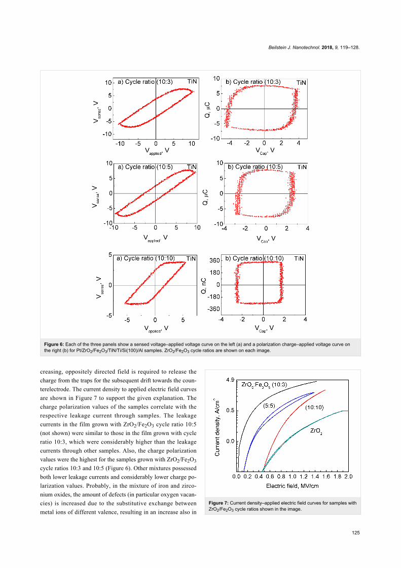
terelectrode. The current density to applied electric field curves
are shown in Figure 7 to support the given explanation. The
charge polarization values of the samples correlate with the
respective leakage current through samples. The leakage
currents in the film grown with ZrO2/Fe2O3 cycle ratio 10:5
(not shown) were similar to those in the film grown with cycle
ratio 10:3, which were considerably higher than the leakage
currents through other samples. Also, the charge polarization
values were the highest for the samples grown with ZrO2/Fe2O3
cycle ratios 10:3 and 10:5 (Figure 6). Other mixtures possessed
both lower leakage currents and considerably lower charge po-
larization values. Probably, in the mixture of iron and zirco-
nium oxides, the amount of defects (in particular oxygen vacan-
cies) is increased due to the substitutive exchange between
metal ions of different valence, resulting in an increase also in
Figure 7: Current density–applied electric field curves for samples withZrO2/Fe2O3 cycle ratios shown in the image.

Beilstein J. Nanotechnol. 2018, 9, 119–128.
126
Figure 8: Selected room temperature magnetization–field curves forZrO2/Fe2O3 films. Cycle ratios and thicknesses are indicated in thelabels.
the leakage currents. Pure ZrO2 exhibited the lowest leakage
current (Figure 7) and did not show any significant charge po-
larization at all.
However, most samples in the present study exhibited ferro-
magnetic-like behavior at room temperature as shown in
Figure 8. Saturation magnetization, reaching M/S = 5 × 10⁻⁶ A
as the maximum value obtained per unit area, could be ob-
served in most samples, but no definite hysteresis was deter-
mined in any case. The ZrO2/Fe2O3 sample with cycle ratio
10:5 (with cation ratio Zr/Fe = 2.0) showed considerably higher
saturation magnetization with the value very similar to that
measured by Sangalli et al. [19]. It is also worth noting that pure
ZrO2 exhibited higher saturation magnetization than other
mixed samples. In the case of a cycle ratio of 10:1 and
Zr/Fe = 50, annealing this sample at 850 °C resulted in the
increase of the observed saturation magnetization. Annealing
the sample with a cycle ratio 10:5 and Zr/Fe = 0.34 at 1000 °C
had an opposite result and removed the saturation magnetiza-
tion of the film (Figure 8).
For comparison with the literature, Myagkov et al. [5] have syn-
thesized Fe–Fe3O4–ZrO2 nanocomposite films by thermally
depositing and oxidizing Fe films, followed by the sequential
deposition of Zr layers and annealing of the double metal
oxide–metal stacks. In this study, saturative magnetization
appeared in the samples heat treated above 250 °C and was re-
corded up to 500 °C, above which nonferromagnetic phases
supposedly started to form. In other studies by de Souza et al.
[33], Kuryliszyn-Kudelska et al. [34] and Okabayashi et al.
[10], only paramagnetic behavior in Fe-doped ZrO2 was ob-
served. One can note that, for example, in the work by
Okabayashi et al. [10], annealing was presumably required in
order to initiate crystallization in sol–gel-synthesized (and
therefore initially amorphous) films. Magnetization-field
hysteresis loops were recorded in the ZrO2 films co-doped with
both iron and cobalt, whereas in the films doped only with 1%
iron, only paramagnetic behavior was observed [10]. In our
films in the present study, the material layers were evidently
crystallized already in the as-deposited state, which was suffi-
cient for the appearance of magnetization loops, However, the
annealing procedure may have resulted in the formation of
nonferromagnetic phases, possibly due to the increased contri-
bution from monoclinic ZrO2 due to the partial compensation of
the oxygen deficiency in the films upon heat treatment in air. It
is, however, worth noting that the recrystallization or transfor-
mation into monoclinic phase cannot be regarded as a fast
process, because there appeared only very weak traces of the
monoclinic polymorph, expressed by an almost insignificantly
low additional reflection at 31.3°, otherwise being indicative of
111 reflection of monoclinic ZrO2 (PDF Card 37-1484). It is
also worth noting that magnetization even in ZrO2 that is not
doped with ferromagnetic metals has been investigated and the-
oretically predicted [43]. In another study on electron beam
evaporated undoped ZrO2 films, ferromagnetic-like magnetiza-
tion hysteresis was recorded, whereby the saturation magnetiza-
tion was positively correlated with the amount of metastable te-
tragonal/cubic zirconia in relation to the stable monoclinic
phase in the films [6].

Beilstein J. Nanotechnol. 2018, 9, 119–128.
127
ConclusionZirconium oxide mixed with iron oxide thin films with various
cycle ratios of constituent oxides were grown by ALD to thick-
nesses ranging from 15 to 40 nm from ZrCl4, Fe(C5H5)2 and
O3. Most of the films exhibited charge polarization and satura-
tion magnetization. The highest numerical values of these phys-
ical quantities were achieved in samples with a relative low iron
content (Zr/Fe > 2.0). The saturation magnetization per unit
area in a film with ZrO2/Fe2O3 cycle ratio of 10:5 was about
5 × 10⁻⁵ A and the charge polarization at 0 V applied voltage
was about 8 µC. These samples were crystallized in the tetrago-
nal/cubic phase of ZrO2. As-deposited samples, in which the
relative cation content for zirconium decreased below 2.0, did
not show any peaks assignable to zirconia.
AcknowledgementsThe present study was partially funded by the European
Regional Development Fund project “Emerging orders in quan-
tum and nanomaterials” (TK134), Spanish Ministry of
Economy and Competitiveness (TEC2014-52152-C3-3-R) with
support of Feder funds, Estonian Academy of Sciences
(SLTFYPROF), and the Estonian Research Agency (IUT2-24,
IUT23-7).
References1. Leskelä, M.; Niinistö, J.; Ritala, M. Atomic Layer Deposition. In
Comprehensive Materials Processing; Cameron, D., Ed.; Elsevier:Amsterdam, Netherlands, 2014; Vol. 4, pp 101–123.doi:10.1016/B978-0-08-096532-1.00401-5
2. Hill, N. A. J. Phys. Chem. B 2000, 104, 6694–6709.doi:10.1021/jp000114x
3. Dimri, M. C.; Khanduri, H.; Kooskora, H.; Kodu, M.; Jaaniso, R.;Heinmaa, I.; Mere, A.; Krustok, J.; Stern, R. J. Phys. D: Appl. Phys.2012, 45, 475003. doi:10.1088/0022-3727/45/47/475003
4. Hong, N. H.; Kanoun, M. B.; Goumri-Said, S.; Song, J.-H.;Chikoidze, E.; Dumont, Y.; Ruyter, A.; Kurisu, M.J. Phys.: Condens. Matter 2013, 25, 436003.doi:10.1088/0953-8984/25/43/436003
5. Myagkov, V. G.; Bykova, L. E.; Bayukov, O. A.; Zhigalov, V. S.;Tambasov, I. A.; Zharkov, S. M.; Matsynin, A. A.; Bondarenko, G. N.J. Alloys Compd. 2015, 636, 223–228.doi:10.1016/j.jallcom.2015.02.012
6. Ning, S.; Zhan, P.; Xie, Q.; Li, Z.; Zhang, Z. J. Phys. D: Appl. Phys.2013, 46, 445004. doi:10.1088/0022-3727/46/44/445004
7. Ning, S.; Zhang, Z. RSC Adv. 2015, 5, 3636–3641.doi:10.1039/C4RA11924J
8. Sahoo, T. R.; Manoharan, S. S.; Lim, S. H.; Salamanca-Riba, L. G.Synth. React. Inorg., Met.-Org., Nano-Met. Chem. 2008, 38, 280–283.
9. Rahman, M. A.; Rout, S.; Thomas, J. P.; McGillivray, D.; Leung, K. T.J. Am. Chem. Soc. 2016, 138, 11896–11906.doi:10.1021/jacs.6b06949
10. Okabayashi, J.; Kono, S.; Yamada, Y.; Nomura, K. AIP Adv. 2011, 1,042138. doi:10.1063/1.3662044
11. Yu, J.; Duan, L. B.; Wang, Y. C.; Rao, G. H. Physica B 2008, 403,4264–4268. doi:10.1016/j.physb.2008.09.015
12. Bechta, S. V.; Krushinov, E. V.; Almjashev, V. I.; Vitol, S. A.;Mezentseva, L. P.; Petrov, Yu. B.; Lopukh, D. B.; Khabensky, V. B.;Barrachin, M.; Hellmann, S.; Froment, K.; Fischer, M.; Tromm, W.;Bottomley, D.; Defoort, F.; Gusarov, V. V. J. Nucl. Mater. 2006, 348,114–121. doi:10.1016/j.jnucmat.2005.09.009
13. Štefanić, G.; Gržeta, B.; Nomura, K.; Trojko, R.; Musić, S.J. Alloys Compd. 2001, 327, 151–160.doi:10.1016/S0925-8388(01)01401-3
14. Kukli, K.; Kemell, M.; Köykkä, J.; Mizohata, K.; Vehkamäki, M.;Ritala, M.; Leskelä, M. Thin Solid Films 2015, 589, 597–604.doi:10.1016/j.tsf.2015.06.033
15. Van Der Voort, P.; van Welzenis, R.; de Ridder, M.; Brongersma, H. H.;Baltes, M.; Mathieu, M.; van de Ven, P. C.; Vansant, E. F. Langmuir2002, 18, 4420–4425. doi:10.1021/la025679u
16. de Ridder, M.; van de Ven, P. C.; van Welzenis, R. G.;Brongersma, H. H.; Helfensteyn, S.; Creemers, C.; Van Der Voort, P.;Baltes, M.; Mathieu, M.; Vansant, E. F. J. Phys. Chem. B 2002, 106,13146–13153. doi:10.1021/jp0211640
17. Lamperti, A.; Cianci, E.; Ciprian, R.; Sangalli, D.; Debernardi, A.Thin Solid Films 2013, 533, 83–87. doi:10.1016/j.tsf.2012.11.127
18. Pitzschel, K.; Bachmann, J.; Montero-Moreno, J. M.; Escrig, J.;Görlitz, D.; Nielsch, K. Nanotechnology 2012, 23, 495718.doi:10.1088/0957-4484/23/49/495718
19. Sangalli, D.; Cianci, E.; Lamperti, A.; Ciprian, R.; Albertini, F.;Casoli, F.; Lupo, P.; Nasi, L.; Campanini, M.; Debernardi, A.Eur. Phys. J. B 2013, 86, 211–216. doi:10.1140/epjb/e2013-30669-3
20. Lin, B.-T.; Lu, Y.-W.; Shieh, J.; Chen, M.-J. J. Eur. Ceram. Soc. 2017,37, 1135–1139. doi:10.1016/j.jeurceramsoc.2016.10.028
21. Pešic, M.; Hoffmann, M.; Richter, C.; Mikolajick, T.; Schroeder, U.Adv. Funct. Mater. 2016, 26, 7486–7494. doi:10.1002/adfm.201603182
22. Arroval, T.; Aarik, L.; Rammula, R.; Kruusla, V.; Aarik, J.Thin Solid Films 2016, 600, 119–125. doi:10.1016/j.tsf.2016.01.024
23. Tamm, A.; Dimri, M. C.; Kozlova, J.; Aidla, A.; Tätte, T.; Arroval, T.;Mäeorg, U.; Mändar, H.; Stern, R.; Kukli, K. J. Cryst. Growth 2012, 343,21–27. doi:10.1016/j.jcrysgro.2011.09.062
24. Martinson, A. B. F.; DeVries, M. J.; Libera, J. A.; Christensen, S. T.;Hupp, J. T.; Pellin, M. J.; Elam, J. W. J. Phys. Chem. C 2011, 115,4333–4339. doi:10.1021/jp110203x
25. Jacqueline, S.; Domengès, B.; Voiron, F.; Murray, H.Semicond. Sci. Technol. 2013, 28, 045018.doi:10.1088/0268-1242/28/4/045018
26. Ritala, M.; Niinistö, J. ECS Trans. 2009, 25, 641–652.doi:10.1149/1.3207651
27. Bae, C.; Shin, H.; Nielsch, K. MRS Bull. 2011, 36, 887–897.doi:10.1557/mrs.2011.264
28. Hughes, K. J.; Engstrom, J. R. J. Vac. Sci. Technol., A 2012, 30,01A102. doi:10.1116/1.3625564
29. Kukli, K.; Ritala, M.; Aarik, J.; Uustare, T.; Leskelä, M. J. Appl. Phys.2002, 92, 1833–1840. doi:10.1063/1.1493657
30. Ritala, M.; Leskelä, M. Appl. Surf. Sci. 1994, 75, 333–340.doi:10.1016/0169-4332(94)90180-5
31. Siimon, H.; Aarik, J. J. Phys. D: Appl. Phys. 1997, 30, 1725–1728.doi:10.1088/0022-3727/30/12/006
32. Lamperti, A.; Lamagna, L.; Congedo, G.; Spiga, S.J. Electrochem. Soc. 2011, 158, G221–G226. doi:10.1149/1.3625254
33. de Souza, A. O.; Ivashita, F. F.; Biondo, V.; Paesano, A., Jr.;Mosca, D. H. J. Alloys Compd. 2016, 680, 701–710.doi:10.1016/j.jallcom.2016.04.170

Beilstein J. Nanotechnol. 2018, 9, 119–128.
128
34. Kuryliszyn-Kudelska, I.; Arciszewska, M.; Małolepszy, A.;Mazurkiewicz, M.; Stobinski, L.; Grabias, A.; Kopcewicz, M.;Paszkowicz, W.; Minikaev, R.; Domukhovski, V.; Nedelko, N.;Dobrowolski, W. J. Alloys Compd. 2015, 632, 609–616.doi:10.1016/j.jallcom.2015.01.257
35. Chakma, S.; Moholkar, V. S. RSC Adv. 2015, 5, 53529–53542.doi:10.1039/c5ra06148b
36. Østreng, E.; Sønsteby, H. H.; Sajavaara, T.; Nilsen, O.; Fjellvåg, H.J. Mater. Chem. C 2013, 1, 4283–4290. doi:10.1039/C3TC30271G
37. Sønsteby, H. H.; Fjellvåg, H.; Nilsen, O. Adv. Mater. Interfaces 2017, 4,1600903. doi:10.1002/admi.201600903
38. Vehkamäki, M.; Hatanpää, T.; Kemell, M.; Ritala, M.; Leskelä, M.Chem. Mater. 2006, 18, 3883–3888. doi:10.1021/cm060966v
39. Zhang, F.; Perng, Y.-C.; Choi, J. H.; Wu, T.; Chung, T.-K.;Carman, G. P.; Locke, C.; Thomas, S.; Saddow, S. E.; Chang, J. P.J. Appl. Phys. 2011, 109, 124109. doi:10.1063/1.3596574
40. Martin, D.; Müller, J.; Schenk, T.; Arruda, T. M.; Kumar, A.; Strelcov, E.;Yurchuk, E.; Müller, S.; Pohl, D.; Schröder, U.; Kalinin, S. V.;Mikolajick, T. Adv. Mater. 2014, 26, 8198–8202.doi:10.1002/adma.201403115
41. Xiang, H.; Shi, F.; Rzchowski, M. S.; Voyles, P. M.; Chang, Y. A.Appl. Phys. Lett. 2010, 97, 092508. doi:10.1063/1.3484278
42. Guo, X. J. Phys. Chem. Solids 1999, 60, 539–546.doi:10.1016/S0022-3697(98)00301-1
43. Máca, F.; Kudrnovský, J.; Drchal, V.; Bouzerar, G. Appl. Phys. Lett.2008, 92, 212503. doi:10.1063/1.2936858
License and TermsThis is an Open Access article under the terms of the
Creative Commons Attribution License
(http://creativecommons.org/licenses/by/4.0), which
permits unrestricted use, distribution, and reproduction in
any medium, provided the original work is properly cited.
The license is subject to the Beilstein Journal of
Nanotechnology terms and conditions:
(http://www.beilstein-journals.org/bjnano)
The definitive version of this article is the electronic one
which can be found at:
doi:10.3762/bjnano.9.14