EL5111, EL5211, EL5411 Datasheet - Intersil.com EL5411 have a bandwidth of 60MHz (-3dB). They also...
19
FN7119 Rev 8.00 Page 1 of 19 August 27, 2015 FN7119 Rev 8.00 August 27, 2015 EL5111, EL5211, EL5411 60MHz Rail-to-Rail Input-Output Op Amps DATASHEET The EL5111, EL5211, and EL5411 are low power, high voltage rail-to-rail input-output amplifiers. The EL5111 represents a single amplifier, the EL5211 contains two amplifiers, and the EL5411 contains four amplifiers. Operating on supplies ranging from 5V to 15V, while consuming only 2.5mA per amplifier, the EL5111, EL5211, and EL5411 have a bandwidth of 60MHz (-3dB). They also provide common mode input ability beyond the supply rails, as well as rail-to-rail output capability. This enables these amplifiers to offer maximum dynamic range at any supply voltage. The EL5111, EL5211, and EL5411 also feature fast slewing and settling times, as well as a high output drive capability of 65mA (sink and source). These features make these amplifiers ideal for high speed filtering and signal conditioning application. Other applications include battery power, portable devices, and anywhere low power consumption is important. The EL5111 is available in 5 Ld TSOT and 8 Ld HMSOP packages. The EL5211 is available in the 8 Ld HMSOP package. The EL5411 is available in space-saving 14 Ld HTSSOP packages. All feature a standard operational amplifier pinout. These amplifiers operate over a temperature range of -40°C to +85°C. Features • Pb-free plus anneal available (RoHS compliant) • 60MHz (-3dB) bandwidth • Supply voltage = 4.5V to 16.5V • Low supply current (per amplifier) = 2.5mA • High slew rate = 75V/µs • Unity-gain stable • Beyond the rails input capability • Rail-to-rail output swing • ±180mA output short current Applications • TFT-LCD panels • V COM amplifiers • Drivers for A/D converters • Data acquisition • Video processing • Audio processing • Active filters • Test equipment • Battery-powered applications • Portable equipment Pinouts EL5111 (8 LD HMSOP) TOP VIEW EL5111 (5 LD TSOT) TOP VIEW EL5211 (8 LD HMSOP) TOP VIEW EL5411 (14 LD HTSSOP) TOP VIEW NC VS+ VOUT NC VS- VIN+ VIN- NC 1 2 3 4 8 7 6 5 - + NO LONGER AVAILABLE OR SUPPORTED 1 2 3 5 4 - + VIN+ VS- VOUT VIN- VS+ VS+ VOUTB VINB- VINB+ VS- VINA+ VINA- VOUTA 1 2 3 4 8 7 6 5 - + - + NO LONGER AVAILABLE OR SUPPORTED - + - + - + - + VS- VS+ VINB+ VINB- VOUTB VINA+ VINA- VOUTA VINC+ VINC- VOUTC VIND+ VIND- VOUTD 1 2 3 4 14 13 12 11 5 6 7 10 9 8 NO LONGER AVAILABLE OR SUPPORTED
Transcript of EL5111, EL5211, EL5411 Datasheet - Intersil.com EL5411 have a bandwidth of 60MHz (-3dB). They also...

FN7119Rev 8.00
August 27, 2015
EL5111, EL5211, EL541160MHz Rail-to-Rail Input-Output Op Amps
DATASHEET
The EL5111, EL5211, and EL5411 are low power, high voltage rail-to-rail input-output amplifiers. The EL5111 represents a single amplifier, the EL5211 contains two amplifiers, and the EL5411 contains four amplifiers. Operating on supplies ranging from 5V to 15V, while consuming only 2.5mA per amplifier, the EL5111, EL5211, and EL5411 have a bandwidth of 60MHz (-3dB). They also provide common mode input ability beyond the supply rails, as well as rail-to-rail output capability. This enables these amplifiers to offer maximum dynamic range at any supply voltage.
The EL5111, EL5211, and EL5411 also feature fast slewing and settling times, as well as a high output drive capability of 65mA (sink and source). These features make these amplifiers ideal for high speed filtering and signal conditioning application. Other applications include battery power, portable devices, and anywhere low power consumption is important.
The EL5111 is available in 5 Ld TSOT and 8 Ld HMSOP packages. The EL5211 is available in the 8 Ld HMSOP package. The EL5411 is available in space-saving 14 Ld HTSSOP packages. All feature a standard operational amplifier pinout. These amplifiers operate over a temperature range of -40°C to +85°C.
Features
• Pb-free plus anneal available (RoHS compliant)
• 60MHz (-3dB) bandwidth
• Supply voltage = 4.5V to 16.5V
• Low supply current (per amplifier) = 2.5mA
• High slew rate = 75V/µs
• Unity-gain stable
• Beyond the rails input capability
• Rail-to-rail output swing
• ±180mA output short current
Applications
• TFT-LCD panels
• VCOM amplifiers
• Drivers for A/D converters
• Data acquisition
• Video processing
• Audio processing
• Active filters
• Test equipment
• Battery-powered applications
• Portable equipment
PinoutsEL5111
(8 LD HMSOP)TOP VIEW
EL5111(5 LD TSOT)TOP VIEW
EL5211(8 LD HMSOP)
TOP VIEW
EL5411(14 LD HTSSOP)
TOP VIEW
NC
VS+
VOUT
NCVS-
VIN+
VIN-
NC 1
2
3
4
8
7
6
5
-+
NO LONGER AVAILABLE O
R SUPPORTED
1
2
3
5
4
-+
VIN+
VS-
VOUT
VIN-
VS+ VS+
VOUTB
VINB-
VINB+VS-
VINA+
VINA-
VOUTA 1
2
3
4
8
7
6
5
-+
-+
NO LONGER AVAILABLE O
R SUPPORTED
-+
-+
-+
-+
VS-VS+
VINB+
VINB-
VOUTB
VINA+
VINA-
VOUTA
VINC+
VINC-
VOUTC
VIND+
VIND-
VOUTD1
2
3
4
14
13
12
11
5
6
7
10
9
8
NO LONGER AVAILABLE O
R SUPPORTED
FN7119 Rev 8.00 Page 1 of 19August 27, 2015

EL5111, EL5211, EL5411
Ordering Information
PART NUMBER PART MARKING TAPE & REEL PACKAGE PKG. DWG. #
EL5111IWTZ-T7 (Note) BAAG 7” (3k pcs) 5 Ld TSOT (Pb-free) MDP0049
EL5111IWTZ-T7A (Note) BAAG 7” (250 pcs) 5 Ld TSOT (Pb-free) MDP0049
EL5111IYEZ (Note) (No longer available or supported)
BAAJA - 8 Ld HMSOP (Pb-free) (3.0mm) MDP0050
EL5111IYEZ-T7 (Note) (No longer available or supported)
BAAJA 7” 8 Ld HMSOP (Pb-free) (3.0mm) MDP0050
EL5111IYEZ-T13 (Note) (No longer available or supported)
BAAJA 13” 8 Ld HMSOP (Pb-free) (3.0mm) MDP0050
EL5211IYEZ (Note) (No longer available or supported)
BAATA - 8 Ld HMSOP (Pb-free) (3.0mm) MDP0050
EL5211IYEZ-T7 (Note) (No longer available or supported)
BAATA 7” 8 Ld HMSOP (Pb-free) (3.0mm) MDP0050
EL5211IYEZ-T13 (Note) (No longer available or supported)
BAATA 13” 8 Ld HMSOP (Pb-free) (3.0mm) MDP0050
EL5411IREZ (Note) (No longer available or supported)
5411IREZ - 14 Ld HTSSOP (Pb-free) (4.4mm) MDP0048
EL5411IREZ-T7 (Note) (No longer available or supported)
5411IREZ 7” 14 Ld HTSSOP (Pb-free) (4.4mm) MDP0048
EL5411IREZ-T13 (Note) (No longer available or supported)
5411IREZ 13” 14 Ld HTSSOP (Pb-free) (4.4mm) MDP0048
EL5411IRZ (Note) (No longer available or supported)
5411IRZ - 14 Ld TSSOP (Pb-free) (4.4mm) M14.173
EL5411IRZ-T7 (Note) (No longer available or supported)
5411IRZ 7” 14 Ld TSSOP (Pb-free) (4.4mm) M14.173
EL5411IRZ-T13 (Note) (No longer available or supported)
5411IRZ 13” 14 Ld TSSOP (Pb-free) (4.4mm) M14.173
NOTE: Intersil Pb-free plus anneal products employ special Pb-free material sets; molding compounds/die attach materials and 100% matte tin plate termination finish, which are RoHS compliant and compatible with both SnPb and Pb-free soldering operations. Intersil Pb-free products are MSL classified at Pb-free peak reflow temperatures that meet or exceed the Pb-free requirements of IPC/JEDEC J STD-020.
FN7119 Rev 8.00 Page 2 of 19August 27, 2015

EL5111, EL5211, EL5411
IMPORTANT NOTE: All parameters having Min/Max specifications are guaranteed. Typ values are for information purposes only. Unless otherwise noted, all tests are at the specified temperature and are pulsed tests, therefore: TJ = TC = TA
Absolute Maximum Ratings (TA = +25°C) Thermal Information
Supply Voltage between VS+ and VS- . . . . . . . . . . . . . . . . . . . .+18VInput Voltage . . . . . . . . . . . . . . . . . . . . . . . . . . VS- - 0.5V, VS +0.5VMaximum Continuous Output Current . . . . . . . . . . . . . . . . . . . 65mAMaximum Die Temperature . . . . . . . . . . . . . . . . . . . . . . . . . .+150°C
Storage Temperature . . . . . . . . . . . . . . . . . . . . . . . . -65°C to +150°CAmbient Operating Temperature . . . . . . . . . . . . . . . . -40°C to +85°CPower Dissipation . . . . . . . . . . . . . . . . . . . . . . . . . . . . . See CurvesPb-free reflow profile . . . . . . . . . . . . . . . . . . . . . . . . . .see link below
http://www.intersil.com/pbfree/Pb-FreeReflow.asp
CAUTION: Stresses above those listed in “Absolute Maximum Ratings” may cause permanent damage to the device. This is a stress only rating and operation of thedevice at these or any other conditions above those indicated in the operational sections of this specification is not implied.
Electrical Specifications VS+ = +5V, VS- = -5V, RL = 1k to 0V, TA = +25°C, Unless Otherwise Specified
PARAMETER DESCRIPTION CONDITIONS MIN TYP MAX UNIT
INPUT CHARACTERISTICS
VOS Input Offset Voltage VCM = 0V 3 15 mV
TCVOS Average Offset Voltage Drift (Note 1) 7 µV/°C
IB Input Bias Current VCM = 0V 2 60 nA
RIN Input Impedance 1 G
CIN Input Capacitance 2 pF
CMIR Common-Mode Input Range -5.5 +5.5 V
CMRR Common-Mode Rejection Ratio for VIN from -5.5V to 5.5V 50 70 dB
AVOL Open-Loop Gain -4.5V VOUT 4.5V 62 70 dB
OUTPUT CHARACTERISTICS
VOL Output Swing Low IL = -5mA -4.92 -4.85 V
VOH Output Swing High IL = 5mA 4.85 4.92 V
ISC Short-Circuit Current ±180 mA
IOUT Output Current ±65 mA
POWER SUPPLY PERFORMANCE
PSRR Power Supply Rejection Ratio VS is moved from ±2.25V to ±7.75V 60 80 dB
IS Supply Current No load (EL5111) 2.5 4.5 mA
No load (EL5211) 5 7.5 mA
No load (EL5411) 10 15 mA
DYNAMIC PERFORMANCE
SR Slew Rate (Note 2) -4.0V VOUT 4.0V, 20% to 80% 75 V/µs
tS Settling to +0.1% (AV = +1) (AV = +1), VO = 2V step 80 ns
BW -3dB Bandwidth 60 MHz
GBWP Gain-Bandwidth Product 32 MHz
PM Phase Margin 50 °
CS Channel Separation f = 5MHz (EL5211 and EL5411 only) 110 dB
dG Differential Gain (Note 3) RF = RG = 1kand VOUT = 1.4V 0.17 %
dP Differential Phase (Note 3) RF = RG = 1kand VOUT = 1.4V 0.24 °
NOTES:
1. Measured over operating temperature range.
2. Slew rate is measured on rising and falling edges.
3. NTSC signal generator used.
FN7119 Rev 8.00 Page 3 of 19August 27, 2015

EL5111, EL5211, EL5411
Electrical Specifications VS+ = +5V, VS- = 0V, RL = 1k to 2.5V, TA = +25°C, Unless Otherwise Specified
PARAMETER DESCRIPTION CONDITION MIN TYP MAX UNIT
INPUT CHARACTERISTICS
VOS Input Offset Voltage VCM = 2.5V 3 15 mV
TCVOS Average Offset Voltage Drift (Note 4) 7 µV/°C
IB Input Bias Current VCM = 2.5V 2 60 nA
RIN Input Impedance 1 G
CIN Input Capacitance 2 pF
CMIR Common-Mode Input Range -0.5 +5.5 V
CMRR Common-Mode Rejection Ratio for VIN from -0.5V to 5.5V 45 66 dB
AVOL Open-Loop Gain 0.5V VOUT 4.5V 62 70 dB
OUTPUT CHARACTERISTICS
VOL Output Swing Low IL = -5mA 80 150 mV
VOH Output Swing High IL = 5mA 4.85 4.92 V
ISC Short-circuit Current ±180 mA
IOUT Output Current ±65 mA
POWER SUPPLY PERFORMANCE
PSRR Power Supply Rejection Ratio VS is moved from 4.5V to 15.5V 60 80 dB
IS Supply Current No load (EL5111) 2.5 4.5 mA
No load (EL5211) 5 7.5 mA
No load (EL5411) 10 15 mA
DYNAMIC PERFORMANCE
SR Slew Rate (Note 5) 1V VOUT 4V, 20% to 80% 75 V/µs
tS Settling to +0.1% (AV = +1) (AV = +1), VO = 2V step 80 ns
BW -3dB Bandwidth 60 MHz
GBWP Gain-Bandwidth Product 32 MHz
PM Phase Margin 50 °
CS Channel Separation f = 5MHz (EL5211 and EL5411 only) 110 dB
dG Differential Gain (Note 6) RF = RG = 1k and VOUT = 1.4V 0.17 %
dP Differential Phase (Note 6) RF = RG = 1k and VOUT = 1.4V 0.24 °
NOTES:
4. Measured over operating temperature range.
5. Slew rate is measured on rising and falling edges.
6. NTSC signal generator used.
FN7119 Rev 8.00 Page 4 of 19August 27, 2015

EL5111, EL5211, EL5411
Electrical Specifications VS+ = +15V, VS- = 0V, RL = 1k to 7.5V, TA = +25°C, Unless Otherwise Specified
PARAMETER DESCRIPTION CONDITION MIN TYP MAX UNIT
INPUT CHARACTERISTICS
VOS Input Offset Voltage VCM = 7.5V 3 15 mV
TCVOS Average Offset Voltage Drift (Note 7) 7 µV/°C
IB Input Bias Current VCM = 7.5V 2 60 nA
RIN Input Impedance 1 G
CIN Input Capacitance 2 pF
CMIR Common-Mode Input Range -0.5 +15.5 V
CMRR Common-Mode Rejection Ratio for VIN from -0.5V to 15.5V 53 72 dB
AVOL Open-Loop Gain 0.5V VOUT 14.5V 62 70 dB
OUTPUT CHARACTERISTICS
VOL Output Swing Low IL = -5mA 80 150 mV
VOH Output Swing High IL = 5mA 14.85 14.92 V
ISC Short-circuit Current ±180 mA
IOUT Output Current ±65 mA
POWER SUPPLY PERFORMANCE
PSRR Power Supply Rejection Ratio VS is moved from 4.5V to 15.5V 60 80 dB
IS Supply Current No load (EL5111) 2.5 4.5 mA
No load (EL5211) 5 7.5 mA
No load (EL5411) 10 15 mA
DYNAMIC PERFORMANCE
SR Slew Rate (Note 8) 1V VOUT 14V, 20% to 80% 75 V/µs
tS Settling to +0.1% (AV = +1) (AV = +1), VO = 2V step 80 ns
BW -3dB Bandwidth 60 MHz
GBWP Gain-Bandwidth Product 32 MHz
PM Phase Margin 50 °
CS Channel Separation f = 5MHz (EL5211 and EL5411 only) 110 dB
dG Differential Gain (Note 9) RF = RG = 1k and VOUT = 1.4V 0.16 %
dP Differential Phase (Note 9) RF = RG = 1k and VOUT = 1.4V 0.22 °
NOTES:
7. Measured over operating temperature range
8. Slew rate is measured on rising and falling edges
9. NTSC signal generator used
FN7119 Rev 8.00 Page 5 of 19August 27, 2015

EL5111, EL5211, EL5411
Typical Performance Curves
FIGURE 1. INPUT OFFSET VOLTAGE DISTRIBUTION FIGURE 2. INPUT OFFSET VOLTAGE DRIFT
FIGURE 3. INPUT OFFSET VOLTAGE vs TEMPERATURE FIGURE 4. INPUT BIAS CURRENT vs TEMPERATURE
FIGURE 5. OUTPUT HIGH VOLTAGE vs TEMPERATURE FIGURE 6. OUTPUT LOW VOLTAGE vs TEMPERATURE
200
QU
AN
TIT
Y (
AM
PL
IFIE
RS
)
INPUT OFFSET VOLTAGE (mV)
0
-12
500
400
100
300
-10 -8 -6 -4 -2 -0 2 4 6 8
10
12
TYPICAL PRODUCTION DISTRIBUTION
VS = ±5VTA = +25°C
INPUT OFFSET VOLTAGE DRIFT, TCVOS (µV/°C)
1 3 5 7 9 11 13
15
17
19
21
5
QU
AN
TIT
Y (
AM
PL
IFIE
RS
)
0
25
15
20
10
VS = ±5V TYPICAL PRODUCTION DISTRIBUTION
0.0
0.5
INP
UT
OF
FS
ET
VO
LTA
GE
(m
V)
TEMPERATURE (°C)
-0.5
1.0
-10-50 30 70 110 150
1.5
2.0
0.000
INP
UT
BIA
S C
UR
RE
NT
(µ
A)
TEMPERATURE (°C)
-0.008
0.008
-0.004
-0.012
0.004
-50 -10 30 70 110 150
VS = ±5V
4.88
4.90
OU
TP
UT
HIG
H V
OLT
AG
E (
V)
4.86
4.96
4.92
4.94
VS = ±5VIOUT = 5mA
TEMPERATURE (°C)
-10-50 30 70 110 150
-4.91
-4.87
OU
TP
UT
LO
W V
OLT
AG
E (
V)
-4.95
-4.85
-4.89
-4.93
VS = ±5VIOUT = 5mA
TEMPERATURE (°C)
-10-50 30 70 110 150
FN7119 Rev 8.00 Page 6 of 19August 27, 2015

EL5111, EL5211, EL5411
FIGURE 7. OPEN-LOOP GAIN vs TEMPERATURE FIGURE 8. SLEW RATE vs TEMPERATURE
FIGURE 9. SUPPLY CURRENT PER AMPLIFIER vs SUPPLY VOLTAGE
FIGURE 10. SUPPLY CURRENT PER AMPLIFIER vs TEMPERATURE
FIGURE 11. DIFFERENTIAL GAIN FIGURE 12. DIFFERENTIAL PHASE
Typical Performance Curves (Continued)
70
OP
EN
-LO
OP
GA
IN (
dB
)
75
60
65
VS = ±5VRL = 1k
TEMPERATURE (°C)
-10-50 30 70 110 150
75
76
SL
EW
RA
TE
(V
/µs)
74
78
73
72
77
VS = ±5V
TEMPERATURE (°C)
-10-50 30 70 110 150
1.7
2.5
SU
PP
LY C
UR
RE
NT
(m
A)
SUPPLY VOLTAGE (V)
1.5
2.9
2.1
2.3
2.7
1.9
TA = +25°C
84 12 16 20
2.45
2.50
SU
PP
LY C
UR
RE
NT
(m
A)
2.40
2.60
2.65
2.55
2.70VS = ±5V
TEMPERATURE (°C)
-10-50 30 70 110 150
-0.16
-0.04
DIF
FE
RE
NT
IAL
GA
IN (
%)
IRE
-0.18
0.00
-0.12
-0.06
-0.02
-0.14
0 100 200
-0.08
-0.10
VS = ±5VAV = 2RL = 1k
0.20
DIF
FE
RE
NT
IAL
PH
AS
E (
°)
IRE
0.00
0.30
0.15
0.25
0 100 200
0.10
0.05
FN7119 Rev 8.00 Page 7 of 19August 27, 2015

EL5111, EL5211, EL5411
FIGURE 13. HARMONIC DISTORTION vs VOP-P FIGURE 14. OPEN LOOP GAIN AND PHASE
FIGURE 15. FREQUENCY RESPONSE FOR VARIOUS RL FIGURE 16. FREQUENCY RESPONSE FOR VARIOUS CL
FIGURE 17. CLOSED LOOP OUTPUT IMPEDANCE FIGURE 18. MAXIMUM OUTPUT SWING vs FREQUENCY
Typical Performance Curves (Continued)
-80
-40
DIS
TO
RT
ION
(d
B)
VOP-P (V)
-90
-30
-60
-50
-70
20 4 6 108
VS = ±5VAV = 2RL = 1kFREQ = 1MHz
3rd HD
2nd HD
GA
IN (
dB
)
60
1k
FREQUENCY (Hz)
PH
AS
E (
°)40
20
250
190
130
70
10
-5010k 100k 1M 10M 100M
80
0
-20
GAIN
PHASE
MA
GN
ITU
DE
(N
OR
MA
LIZ
ED
) (d
B) 5
3
FREQUENCY (Hz)
1
-1
-3
-5100k 1M 100M
1k
10M
150
VS = ±5VAV = 1 CLOAD = 0pF
560
MA
GN
ITU
DE
(N
OR
MA
LIZ
ED
) (d
B)
FREQUENCY (Hz)
25
15
5
-5
-15
-25100k 1M 100M10M
1000pF100pF
47pF
10pF
VS = ±5VAV = 1 RL = 1k
OU
TP
UT
IM
PE
DA
NC
E (
)
400
350
FREQUENCY (Hz)
300
250
200
010k 100k 100M1M 10M
150
100
502
10
MA
XIM
UM
OU
TP
UT
SW
ING
(V
P-P
)
FREQUENCY (kHz)
0
12
6
8
4
100k10k 1M 100M10M
VS = ±5VAV = 1RL = 1kDISTORTION <1%
FN7119 Rev 8.00 Page 8 of 19August 27, 2015

EL5111, EL5211, EL5411
FIGURE 19. CMRR FIGURE 20. PSRR
FIGURE 21. INPUT VOLTAGE NOISE SPECTRAL DENSITY FIGURE 22. CHANNEL SEPARATION
FIGURE 23. SMALL-SIGNAL OVERSHOOT vs LOAD CAPACITANCE
FIGURE 24. SETTLING TIME vs STEP SIZE
Typical Performance Curves (Continued)C
MR
R (
dB
)
-15
FREQUENCY (Hz)
-45
-651k 10k 100M1M 10M
-55
100k
-25
-35
0
PS
RR
(d
B)
-80
-60
-40
-20
PSRR+
FREQUENCY (Hz)
100 1k 10M100k 1M10k
PSRR-
VS = ±5VTA = +25°C
10
100
VO
LTA
GE
NO
ISE
(n
V/
Hz)
FREQUENCY (Hz)
1
1K
100 1k 100M1M 10M100k10k
-60
XTA
LK
(d
B)
-160
-120
-100
-80
DUAL MEASURED CH A TO BQUAD MEASURED CH A TO D OR B TO COTHER COMBINATIONS YIELD IMPROVED REJECTION
VS = ±5VRL = 1kAV = 1VIN = 110mVRMS
-140
FREQUENCY (Hz)
1k 10k 10M 30M1M100k
LOAD CAPACITANCE (pF)
OV
ER
SH
OO
T (
%)
VS = ±5VAV = 1RL = 1kVIN = ±50mVTA = +25°C
10 1k100
100
0
40
60
80
20
-4
4
ST
EP
SIZ
E (
V)
SETTLING TIME (ns)
-5
5
0
2
-2
6555 75 10595
VS = ±5VAV = 1RL = 1k
85
3
-1
1
-3 0.1%
0.1%
FN7119 Rev 8.00 Page 9 of 19August 27, 2015

EL5111, EL5211, EL5411
FIGURE 25. LARGE SIGNAL TRANSIENT RESPONSE FIGURE 26. SMALL SIGNAL TRANSIENT RESPONSE
Typical Performance Curves (Continued)
50ns/DIV
1V STEP
VS = ±5VTA = +25°CAV = 1RL = 1k
50ns/DIV
100mV STEP
VS = ±5VTA = +25°CAV = 1RL = 1k
Pin Descriptions
EL5111 (TSOT-5)
EL5111 (HMSOP8)
EL5211 (HMSOP8)
EL5411 (HTSSOP14) NAME FUNCTION EQUIVALENT CIRCUIT
1 6 1 1 VOUTA Amplifier A output
4 2 2 2 VINA- Amplifier A inverting input
3 3 3 3 VINA+ Amplifier A non-inverting input (Reference Circuit 2)
5 7 8 4 VS+ Positive power supply
5 5 VINB+ Amplifier B non-inverting input (Reference Circuit 2)
6 6 VINB- Amplifier B inverting input (Reference Circuit 2)
7 7 VOUTB Amplifier B output (Reference Circuit 1)
8 VOUTC Amplifier C output (Reference Circuit 1)
9 VINC- Amplifier C inverting input (Reference Circuit 2)
10 VINC+ Amplifier C non-inverting input (Reference Circuit 2)
2 4 4 11 VS- Negative power supply
12 VIND+ Amplifier D non-inverting input (Reference Circuit 2)
13 VIND- Amplifier D inverting input (Reference Circuit 2)
14 VOUTD Amplifier D output (Reference Circuit 1)
1, 5, 8 NC Not connected
VS+
GNDVS-
CIRCUIT 1
VS+
VS-
CIRCUIT 2
FN7119 Rev 8.00 Page 10 of 19August 27, 2015

EL5111, EL5211, EL5411
Applications Information
Product Description
The EL5111, EL5211, and EL5411 voltage feedback amplifiers are fabricated using a high voltage CMOS process. They exhibit rail-to-rail input and output capability, are unity gain stable and have low power consumption (2.5mA per amplifier). These features make the EL5111, EL5211, and EL5411 ideal for a wide range of general-purpose applications. Connected in voltage follower mode and driving a load of 1k, the EL5111, EL5211, and EL5411 have a -3dB bandwidth of 60MHz while maintaining a 75V/µs slew rate. The EL5111 is a single amplifier, the EL5211 a dual amplifier, and the EL5411 a quad amplifier.
Operating Voltage, Input, and Output
The EL5111, EL5211, and EL5411 are specified with a single nominal supply voltage from 5V to 15V or a split supply with its total range from 5V to 15V. Correct operation is guaranteed for a supply range of 4.5V to 16.5V. Most EL5111, EL5211, and EL5411 specifications are stable over both the full supply range and operating temperatures of -40°C to +85°C. Parameter variations with operating voltage and/or temperature are shown in the typical performance curves.
The input common-mode voltage range of the EL5111, EL5211, and EL5411 extends 500mV beyond the supply rails. The output swings of the EL5111, EL5211, and EL5411 typically extend to within 100mV of positive and negative supply rails with load currents of 5mA. Decreasing load currents will extend the output voltage range even closer to the supply rails. Figure 27 shows the input and output waveforms for the device in the unity-gain configuration. Operation is from ±5V supply with a 1k load connected to GND. The input is a 10VP-P sinusoid. The output voltage is approximately 9.8VP-P.
Short Circuit Current Limit
The EL5111, EL5211, and EL5411 will limit the short circuit current to ±180mA if the output is directly shorted to the positive or the negative supply. If an output is shorted indefinitely, the power dissipation could easily increase such that the device may be damaged. Maximum reliability is maintained if the output continuous current never exceeds ±65mA. This limit is set by the design of the internal metal interconnects.
Output Phase Reversal
The EL5111, EL5211, and EL5411 are immune to phase reversal as long as the input voltage is limited from VS- -0.5V to VS+ +0.5V. Figure 28 shows a photo of the output of the device with the input voltage driven beyond the supply rails. Although the device's output will not change phase, the input's overvoltage should be avoided. If an input voltage exceeds supply voltage by more than 0.6V, electrostatic protection diodes placed in the input stage of the device begin to conduct and overvoltage damage could occur.
Power Dissipation
With the high-output drive capability of the EL5111, EL5211, and EL5411 amplifiers, it is possible to exceed the +125°C 'absolute-maximum junction temperature' under certain load current conditions. Therefore, it is important to calculate the maximum junction temperature for the application to determine if load conditions need to be modified for the amplifier to remain in the safe operating area.
The maximum power dissipation allowed in a package is determined according to:
where:
• TJMAX = Maximum junction temperature
• TAMAX = Maximum ambient temperature
• JA = Thermal resistance of the package
• PDMAX = Maximum power dissipation in the package
OU
TP
UT
INP
UT
5V
5V 10µs
VS = ±5V, TA = +25°C, AV = 1, VIN = 10VP-P
FIGURE 27. OPERATION WITH RAIL-TO-RAIL INPUT AND OUTPUT
1V
1V 10µs
VS = ±2.5V, TA = +25°C, AV = 1, VIN = 6VP-P
FIGURE 28. OPERATION WITH BEYOND-THE-RAILS INPUT
PDMAX
TJMAX TAMAX–
JA---------------------------------------------=
(EQ. 1)
FN7119 Rev 8.00 Page 11 of 19August 27, 2015

EL5111, EL5211, EL5411
The maximum power dissipation actually produced by an IC is the total quiescent supply current times the total power supply voltage, plus the power in the IC due to the loads, or:
when sourcing, and:
when sinking,
where:
• i = 1 to 2 for dual and 1 to 4 for quad
• VS = Total supply voltage
• ISMAX = Maximum supply current per amplifier
• VOUTi = Maximum output voltage of the application
• ILOADi = Load current
If we set the two PDMAX equations equal to each other, we can solve for RLOADi to avoid device overheat. Figures 29 through 36 provide a convenient way to see if the device will overheat. The maximum safe power dissipation can be found graphically, based on the package type and the ambient temperature. By using the previous equation, it is a simple matter to see if PDMAX exceeds the device's power derating curves. To ensure proper operation, it is important to observe the recommended derating curves shown in Figures 29 through 36.
PDMAX i V S ISMAX V S+ VOUTi ILOADi–+ =(EQ. 2)
PDMAX i V S ISMAX V OUTi VS- ILOADi–+ =(EQ. 3)
FIGURE 29. PACKAGE POWER DISSIPATION vs AMBIENT TEMPERATURE
JEDEC JESD51-3 LOW EFFECTIVE THERMAL CONDUCTIVITY TEST BOARD
0.9
0.8
0.6
0.4
0.3
0.2
0.1
0.00 25 50 75 100 125
AMBIENT TEMPERATURE (°C)
PO
WE
R D
ISS
IPA
TIO
N (
W)
85
0.7
0.5
694mW
JA = +144°C/W
HTSSOP14
FIGURE 30. PACKAGE POWER DISSIPATION vs AMBIENT TEMPERATURE
JEDEC JESD51-7 HIGH EFFECTIVE THERMAL CONDUCTIVITY (4-LAYER) TEST BOARD - HTSSOP EXPOSED DIEPAD SOLDERED TO PCB PER JESD51-5
3.5
3.0
2.0
1.0
0.5
0.00 25 50 75 100 125
AMBIENT TEMPERATURE (°C)
PO
WE
R D
ISS
IPA
TIO
N (
W)
85
2.632W
2.5
1.5
JA = +38°C/W
HTSSOP14
JEDEC JESD51-3 LOW EFFECTIVE THERMAL CONDUCTIVITY TEST BOARD
1.2
1.0
0.8
0.4
0.2
0.00 25 50 75 100 150
AMBIENT TEMPERATURE (°C)
PO
WE
R D
ISS
IPA
TIO
N (
W)
1.042W
977mW
893mW
JA = +140°C/W
TSSOP20
JA = +128°C/W
TSSOP24
JA = +120°C/W
TSSOP28
12585
0.6
JA = +165°C/W
TSSOP14
JA = +148°C/W
TSSOP16
845mW
758mW
FIGURE 31. PACKAGE POWER DISSIPATION vs AMBIENT TEMPERATURE
JEDEC JESD51-7 HIGH EFFECTIVE THERMAL CONDUCTIVITY TEST BOARD
1.8
1.6
1.2
0.6
0.4
0.00 25 50 75 100 150
AMBIENT TEMPERATURE (°C)
PO
WE
R D
ISS
IPA
TIO
N (
W)
1.667W
1.471W
1.389W
JA=+90°C/W
TSSOP20
JA=+85°C/W
TSSOP24
JA=+75°C/W
TSSOP28
12585
0.8
JA=+100°C/W
TSSOP14
JA=+97°C/W
TSSOP16
1.289W
1.250W
1.4
1.0
0.2
FIGURE 32. PACKAGE POWER DISSIPATION vs AMBIENT TEMPERATURE
FN7119 Rev 8.00 Page 12 of 19August 27, 2015

EL5111, EL5211, EL5411
Unused Amplifiers
It is recommended that any unused amplifiers in a dual and a quad package be configured as a unity gain follower. The inverting input should be directly connected to the output and the non-inverting input tied to the ground plane.
Power Supply Bypassing and Printed Circuit Board Layout
The EL5111, EL5211, and EL5411 can provide gain at high frequency. As with any high-frequency device, good printed circuit board layout is necessary for optimum performance. Ground plane construction is highly recommended, lead lengths should be as short as possible and the power supply pins must be well bypassed to reduce the risk of oscillation. For normal single supply operation, where the VS- pin is connected to ground, a 0.1µF ceramic capacitor should be placed from VS+ to pin to VS- pin. A 4.7µF tantalum capacitor should then be connected in parallel, placed in the region of the amplifier. One 4.7µF capacitor may be used for multiple devices. This same capacitor combination should be placed at each supply pin to ground if split supplies are to be used.
FIGURE 33. PACKAGE POWER DISSIPATION vs AMBIENT TEMPERATURE
FIGURE 34. PACKAGE POWER DISSIPATION vs AMBIENT TEMPERATURE
FIGURE 35. PACKAGE POWER DISSIPATION vs AMBIENT TEMPERATURE
FIGURE 36. PACKAGE POWER DISSIPATION vs AMBIENT TEMPERATURE
JEDEC JESD51-3 LOW EFFECTIVE THERMAL CONDUCTIVITY (SINGLE LAYER) TEST BOARD
PO
WE
R D
ISS
IPA
TIO
N (
W) 0.300
0.250
0.200
0.150
0.100
0.050
0.000
0.350
AMBIENT TEMPERATURE (°C)
0 25 50 75 100 12585 150
290mW
TSOT5JA = +345°C/W
0.6
0.5
0.4
0.3
0.2
0.1
0.0
JEDEC JESD51-7 HIGH EFFECTIVE THERMAL CONDUCTIVITY (4-LAYER) TEST BOARD
483mW
TSOT5
AMBIENT TEMPERATURE (°C)
PO
WE
R D
ISS
IPA
TIO
N (
W)
0 25 50 75 100 12585 150
JA = +207°C/W
JEDEC JESD51-3 LOW EFFECTIVE THERMAL CONDUCTIVITY TEST BOARD
0.6
0.4
0.3
0.2
0.1
00 25 50 75 100 125
AMBIENT TEMPERATURE (°C)
PO
WE
R D
ISS
IPA
TIO
N (
W)
85
486mW
JA = +206°C/W
HMSOP8
0.5
JEDEC JESD51-7 HIGH EFFECTIVE THERMAL CONDUCTIVITY TEST BOARD
1
0.9
0.6
0.4
0.3
0.2
0.1
00 25 50 75 100 125
AMBIENT TEMPERATURE (°C)
PO
WE
R D
ISS
IPA
TIO
N (
W)
85
870mW
JA = +115°C/W
HMSOP8
0.8
0.5
0.7
FN7119 Rev 8.00 Page 13 of 19August 27, 2015

EL5111, EL5211, EL5411
About IntersilIntersil Corporation is a leading provider of innovative power management and precision analog solutions. The company's products address some of the largest markets within the industrial and infrastructure, mobile computing and high-end consumer markets.
For the most updated datasheet, application notes, related documentation and related parts, please see the respective product information page found at www.intersil.com.
You may report errors or suggestions for improving this datasheet by visiting www.intersil.com/ask.
Reliability reports are also available from our website at www.intersil.com/support
Revision HistoryThe revision history provided is for informational purposes only and is believed to be accurate, but not warranted. Please go to the web to make sure that you have the latest revision.
DATE REVISION CHANGE
August 27, 2015 FN7119.8 Updated Ordering Information Table on page 2.Added Revision History and About Intersil sections.
FN7119 Rev 8.00 Page 14 of 19August 27, 2015

EL5111, EL5211, EL5411
FN7119 Rev 8.00 Page 15 of 19August 27, 2015
Thin Shrink Small Outline Package Family (TSSOP)
N (N/2)+1
(N/2)
TOP VIEW
AD
0.20 C2X
B A
N/2 LEAD TIPSB
E1E
0.25 C A BM
1
H
PIN #1 I.D.
0.05e
C
0.10 C
N LEADS SIDE VIEW
0.10 C A BMb
c
SEE DETAIL “X”
END VIEW
DETAIL X
A2
0° - 8°
GAUGEPLANE
0.25
LA1
A
L1
SEATINGPLANE
MDP0044THIN SHRINK SMALL OUTLINE PACKAGE FAMILY
SYMBOL
MILLIMETERS
TOLERANCE14 LD 16 LD 20 LD 24 LD 28 LD
A 1.20 1.20 1.20 1.20 1.20 Max
A1 0.10 0.10 0.10 0.10 0.10 ±0.05
A2 0.90 0.90 0.90 0.90 0.90 ±0.05
b 0.25 0.25 0.25 0.25 0.25 +0.05/-0.06
c 0.15 0.15 0.15 0.15 0.15 +0.05/-0.06
D 5.00 5.00 6.50 7.80 9.70 ±0.10
E 6.40 6.40 6.40 6.40 6.40 Basic
E1 4.40 4.40 4.40 4.40 4.40 ±0.10
e 0.65 0.65 0.65 0.65 0.65 Basic
L 0.60 0.60 0.60 0.60 0.60 ±0.15
L1 1.00 1.00 1.00 1.00 1.00 Reference
Rev. F 2/07NOTES:
1. Dimension “D” does not include mold flash, protrusions or gate burrs. Mold flash, protrusions or gate burrs shall not exceed0.15mm per side.
2. Dimension “E1” does not include interlead flash or protrusions. Interlead flash and protrusions shall not exceed 0.25mm perside.
3. Dimensions “D” and “E1” are measured at dAtum Plane H.
4. Dimensioning and tolerancing per ASME Y14.5M-1994.

EL5111, EL5211, EL5411
FN7119 Rev 8.00 Page 16 of 19August 27, 2015
HTSSOP (Heat-Sink TSSOP) Family
N (N/2)+1
(N/2)
TOP VIEW
AD
0.20 C2X
B A
N/2 LEAD TIPSB
E1E
0.25 C A BM
1
H
PIN #1 I.D.
0.05e
C
0.10 C
N LEADS SIDE VIEW
0.10 C A BMb
c
SEE DETAIL “X”
END VIEW
DETAIL X
A2
0° - 8°
GAUGEPLANE
0.25
LA1
A
L1
SEATINGPLANE
BOTTOM VIEW
EXPOSED THERMAL PAD
E2
D1
MDP0048HTSSOP (HEAT-SINK TSSOP) FAMILY
SYMBOL
MILLIMETERS
TOLERANCE14 LD 20 LD 24 LD 28 LD 38 LD
A 1.20 1.20 1.20 1.20 1.20 Max
A1 0.075 0.075 0.075 0.075 0.075 ±0.075
A2 0.90 0.90 0.90 0.90 0.90 +0.15/-0.10
b 0.25 0.25 0.25 0.25 0.22 +0.05/-0.06
c 0.15 0.15 0.15 0.15 0.15 +0.05/-0.06
D 5.00 6.50 7.80 9.70 9.70 ±0.10
D1 3.2 4.2 4.3 5.0 7.25 Reference
E 6.40 6.40 6.40 6.40 6.40 Basic
E1 4.40 4.40 4.40 4.40 4.40 ±0.10
E2 3.0 3.0 3.0 3.0 3.0 Reference
e 0.65 0.65 0.65 0.65 0.50 Basic
L 0.60 0.60 0.60 0.60 0.60 ±0.15
L1 1.00 1.00 1.00 1.00 1.00 Reference
N 14 20 24 28 38 Reference
Rev. 3 2/07NOTES:
1. Dimension “D” does not include mold flash, protrusions or gate burrs. Mold flash, protrusions or gate burrs shall not exceed0.15mm per side.
2. Dimension “E1” does not include interlead flash or protrusions. Interlead flash and protrusions shall not exceed 0.25mm perside.
3. Dimensions “D” and “E1” are measured at Datum Plane H.
4. Dimensioning and tolerancing per ASME Y14.5M-1994.
EL5111, EL5211, EL5411
FN7119 Rev 8.00 Page 17 of 19August 27, 2015
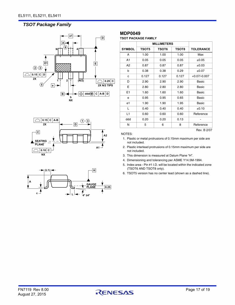
TSOT Package Family
e1
N
A
D
E
4
(N/2)21
E1
0.15 DC
2X0.25 C
2X N/2 TIPSe
B ddd M DC A-Bb
NX
6
2 3
5
SEATINGPLANE
0.10 C
NX
1 3
C
D
0.15 A-BC
2X
A2
A1
H
c
(L1)
L
0.25
4° ±4°
GAUGEPLANE
A
MDP0049TSOT PACKAGE FAMILY
SYMBOL
MILLIMETERS
TOLERANCETSOT5 TSOT6 TSOT8
A 1.00 1.00 1.00 Max
A1 0.05 0.05 0.05 ±0.05
A2 0.87 0.87 0.87 ±0.03
b 0.38 0.38 0.29 ±0.07
c 0.127 0.127 0.127 +0.07/-0.007
D 2.90 2.90 2.90 Basic
E 2.80 2.80 2.80 Basic
E1 1.60 1.60 1.60 Basic
e 0.95 0.95 0.65 Basic
e1 1.90 1.90 1.95 Basic
L 0.40 0.40 0.40 ±0.10
L1 0.60 0.60 0.60 Reference
ddd 0.20 0.20 0.13 -
N 5 6 8 Reference
Rev. B 2/07NOTES:
1. Plastic or metal protrusions of 0.15mm maximum per side are not included.
2. Plastic interlead protrusions of 0.15mm maximum per side are not included.
3. This dimension is measured at Datum Plane “H”.
4. Dimensioning and tolerancing per ASME Y14.5M-1994.
5. Index area - Pin #1 I.D. will be located within the indicated zone (TSOT6 AND TSOT8 only).
6. TSOT5 version has no center lead (shown as a dashed line).

EL5111, EL5211, EL5411
FN7119 Rev 8.00 Page 18 of 19August 27, 2015
HMSOP (Heat-Sink MSOP) Package Family
1
(N/2)
(N/2)+1
N
PLANESEATING
N LEADS0.10 C
PIN #1I.D.
E1
E
b
DETAIL X3° ±3°
GAUGEPLANE
SEE DETAIL "X"
c
A
0.25
A2
A1L
0.25 C A B
D
A
M
B
e
C
0.08 C A BM
H
L1
END VIEW
SIDE VIEW
TOP VIEW
E2
BOTTOM VIEW
D1
EXPOSED THERMAL PAD
MDP0050HMSOP (HEAT-SINK MSOP) PACKAGE FAMILY
SYMBOL
MILLIMETERS
TOLERANCE NOTESHMSOP8 HMSOP10
A 1.00 1.00 Max. -
A1 0.075 0.075 +0.025/-0.050 -
A2 0.86 0.86 ±0.09 -
b 0.30 0.20 +0.07/-0.08 -
c 0.15 0.15 ±0.05 -
D 3.00 3.00 ±0.10 1, 3
D1 1.85 1.85 Reference -
E 4.90 4.90 ±0.15 -
E1 3.00 3.00 ±0.10 2, 3
E2 1.73 1.73 Reference -
e 0.65 0.50 Basic -
L 0.55 0.55 ±0.15 -
L1 0.95 0.95 Basic -
N 8 10 Reference -
Rev. 1 2/07NOTES:
1. Plastic or metal protrusions of 0.15mm maximum per side are not included.
2. Plastic interlead protrusions of 0.25mm maximum per side are not included.
3. Dimensions “D” and “E1” are measured at Datum Plane “H”.
4. Dimensioning and tolerancing per ASME Y14.5M-1994.

FN7119 Rev 8.00 Page 19 of 19August 27, 2015
EL5111, EL5211, EL5411
Intersil products are manufactured, assembled and tested utilizing ISO9001 quality systems as notedin the quality certifications found at www.intersil.com/en/support/qualandreliability.html
Intersil products are sold by description only. Intersil may modify the circuit design and/or specifications of products at any time without notice, provided that such modification does not, in Intersil's sole judgment, affect the form, fit or function of the product. Accordingly, the reader is cautioned to verify that datasheets are current before placing orders. Information furnished by Intersil is believed to be accurate and reliable. However, no responsibility is assumed by Intersil or its subsidiaries for its use; nor for any infringements of patents or other rights of third parties which may result from its use. No license is granted by implication or otherwise under any patent or patent rights of Intersil or its subsidiaries.
For information regarding Intersil Corporation and its products, see www.intersil.com
For additional products, see www.intersil.com/en/products.html
© Copyright Intersil Americas LLC 2004-2015. All Rights Reserved.All trademarks and registered trademarks are the property of their respective owners.
Thin Shrink Small Outline Plastic Packages (TSSOP)
INDEXAREA
E1
D
N
1 2 3
-B-
0.10(0.004) C AM B S
e
-A-
b
M
-C-
A1
A
SEATING PLANE
0.10(0.004)
c
E 0.25(0.010) BM M
L0.25
0.010
GAUGEPLANE
A2
NOTES:
1. These package dimensions are within allowable dimensions of JEDEC MO-153-AC, Issue E.
2. Dimensioning and tolerancing per ANSI Y14.5M-1982.
3. Dimension “D” does not include mold flash, protrusions or gate burrs. Mold flash, protrusion and gate burrs shall not exceed 0.15mm(0.006 inch) per side.
4. Dimension “E1” does not include interlead flash or protrusions. Inter-lead flash and protrusions shall not exceed 0.15mm (0.006 inch) perside.
5. The chamfer on the body is optional. If it is not present, a visual index feature must be located within the crosshatched area.
6. “L” is the length of terminal for soldering to a substrate.
7. “N” is the number of terminal positions.
8. Terminal numbers are shown for reference only.
9. Dimension “b” does not include dambar protrusion. Allowable dambar protrusion shall be 0.08mm (0.003 inch) total in excess of “b” dimen-sion at maximum material condition. Minimum space between protru-sion and adjacent lead is 0.07mm (0.0027 inch).
10. Controlling dimension: MILLIMETER. Converted inch dimensions are not necessarily exact. (Angles in degrees)
0.05(0.002)
M14.17314 LEAD THIN SHRINK SMALL OUTLINE PLASTIC PACKAGE
SYMBOL
INCHES MILLIMETERS
NOTESMIN MAX MIN MAX
A - 0.047 - 1.20 -
A1 0.002 0.006 0.05 0.15 -
A2 0.031 0.041 0.80 1.05 -
b 0.0075 0.0118 0.19 0.30 9
c 0.0035 0.0079 0.09 0.20 -
D 0.195 0.199 4.95 5.05 3
E1 0.169 0.177 4.30 4.50 4
e 0.026 BSC 0.65 BSC -
E 0.246 0.256 6.25 6.50 -
L 0.0177 0.0295 0.45 0.75 6
N 14 14 7
0o 8o 0o 8o -
Rev. 2 4/06