![[Book] CMOS Current Amplifiers](https://static.fdocuments.in/doc/165x107/54e62e884a7959e23f8b47cb/book-cmos-current-amplifiers.jpg)
Low-Cost, CMOS, Rail-to-Rail, I/O OPERATIONAL AMPLIFIERS · OPA705 OPA2705 OPA4705 Low-Cost, CMOS,...
15
OPA705 OPA2705 OPA4705 Low-Cost, CMOS, Rail-to-Rail, I/O OPERATIONAL AMPLIFIERS FEATURES ● RAIL-TO-RAIL INPUT AND OUTPUT ● WIDE SUPPLY RANGE: Single Supply: 4V to 12V Dual Supplies: ±2 to ± 6 ● LOW QUIESCENT CURRENT: 160µA ● LIMITED RANGE CMRR: 96dB ● LOW OFFSET: 0.5mV ● HIGH SPEED: 1MHz, 0.6V/ µ s ● MicroSIZE PACKAGES: SOT23-5, MSOP-8, TSSOP-14 ● LOW INPUT BIAS CURRENT: 1pA APPLICATIONS ● AUTOMOTIVE APPLICATIONS: Audio, Sensor Applications, Security Systems ● PORTABLE EQUIPMENT ● ACTIVE FILTERS ● TRANSDUCER AMPLIFIER ● TEST EQUIPMENT ● DATA ACQUISITION DESCRIPTION The OPA705 series low-cost op amps are optimized for appli- cations requiring rail-to-rail input and output swing. Single, dual, and quad versions are offered in a variety of packages. While the quiescent current is less than 200µA per amplifier, the OPA705 still offers excellent dynamic performance (1MHz GBW and 0.6V/µs SR) and unity-gain stability. The OPA705 series is fully specified and guaranteed over the supply range of ±2V to ±6V. Input swing extends 300mV beyond the rail and the output swings to within 40mV of the rail. The single version (OPA705) is available in the MicroSIZE SOT23-5 and in the standard SO-8 surface-mount packages. The dual version (OPA2705) is available in the MSOP-8, SO-8, and DIP-8 packages. The quad OPA4705 is available in the TSSOP-14 and SO-14 packages. All are specified for operation from –40°C to +85°C. 1 2 3 5 4 V+ –In Out V– +In OPA705 SOT23-5 1 2 3 4 8 7 6 5 NC V+ Out NC NC –In +In V– OPA705 SO-8, DIP-8 1 2 3 4 8 7 6 5 V+ Out B –In B +In B Out A –In A +In A V– OPA2705 MSOP-8, SO-8, DIP-8 A B 1 2 3 4 5 6 7 14 13 12 11 10 9 8 Out D –In D +In D V– +In C –In C Out C Out A –In A +In A V+ +In B –In B Out B OPA4705 TSSOP-14, SO-14 A D B C SBOS182A – JUNE 2001 www.ti.com PRODUCTION DATA information is current as of publication date. Products conform to specifications per the terms of Texas Instruments standard warranty. Production processing does not necessarily include testing of all parameters. Copyright © 2001, Texas Instruments Incorporated Please be aware that an important notice concerning availability, standard warranty, and use in critical applications of Texas Instruments semiconductor products and disclaimers thereto appears at the end of this data sheet. ® OPA705 OPA705 OPA705 OPA705
Transcript of Low-Cost, CMOS, Rail-to-Rail, I/O OPERATIONAL AMPLIFIERS · OPA705 OPA2705 OPA4705 Low-Cost, CMOS,...

OPA705OPA2705OPA4705
Low-Cost, CMOS, Rail-to-Rail, I/OOPERATIONAL AMPLIFIERS
FEATURES RAIL-TO-RAIL INPUT AND OUTPUT WIDE SUPPLY RANGE:
Single Supply: 4V to 12VDual Supplies: ±2 to ±6
LOW QUIESCENT CURRENT: 160µA LIMITED RANGE CMRR: 96dB LOW OFFSET: 0.5mV HIGH SPEED: 1MHz, 0.6V/µs MicroSIZE PACKAGES:
SOT23-5, MSOP-8, TSSOP-14 LOW INPUT BIAS CURRENT: 1pA
APPLICATIONS AUTOMOTIVE APPLICATIONS:
Audio, Sensor Applications, Security Systems PORTABLE EQUIPMENT ACTIVE FILTERS TRANSDUCER AMPLIFIER TEST EQUIPMENT DATA ACQUISITION
DESCRIPTIONThe OPA705 series low-cost op amps are optimized for appli-cations requiring rail-to-rail input and output swing. Single,dual, and quad versions are offered in a variety of packages.While the quiescent current is less than 200µA per amplifier,the OPA705 still offers excellent dynamic performance(1MHz GBW and 0.6V/µs SR) and unity-gain stability.
The OPA705 series is fully specified and guaranteed overthe supply range of ±2V to ±6V. Input swing extends300mV beyond the rail and the output swings to within40mV of the rail.
The single version (OPA705) is available in the MicroSIZESOT23-5 and in the standard SO-8 surface-mount packages.The dual version (OPA2705) is available in the MSOP-8,SO-8, and DIP-8 packages. The quad OPA4705 is availablein the TSSOP-14 and SO-14 packages. All are specified foroperation from –40°C to +85°C.
1
2
3
5
4
V+
–In
Out
V–
+In
OPA705
SOT23-5
1
2
3
4
8
7
6
5
NC
V+
Out
NC
NC
–In
+In
V–
OPA705
SO-8, DIP-8
1
2
3
4
8
7
6
5
V+
Out B
–In B
+In B
Out A
–In A
+In A
V–
OPA2705
MSOP-8, SO-8, DIP-8
A
B
1
2
3
4
5
6
7
14
13
12
11
10
9
8
Out D
–In D
+In D
V–
+In C
–In C
Out C
Out A
–In A
+In A
V+
+In B
–In B
Out B
OPA4705
TSSOP-14, SO-14
A D
B C
SBOS182A – JUNE 2001
www.ti.com
PRODUCTION DATA information is current as of publication date.Products conform to specifications per the terms of Texas Instrumentsstandard warranty. Production processing does not necessarily includetesting of all parameters.
Copyright © 2001, Texas Instruments Incorporated
Please be aware that an important notice concerning availability, standard warranty, and use in critical applications ofTexas Instruments semiconductor products and disclaimers thereto appears at the end of this data sheet.
®OPA705
OPA705
OPA705
OPA705

OPA705, 2705, 47052SBOS182A
MINIMUM PACKAGERECOMMENDED DRAWING PACKAGE ORDERING TRANSPORT
PRODUCT DESCRIPTION GAIN PACKAGE NUMBER MARKING NUMBER(1) MEDIA
OPA705NA Single, GBW = 1MHz 1 SOT23-5 331 A05 OPA705NA/250 Tape and Reel" " " " " " OPA705NA/3K Tape and Reel
OPA705UA Single, GBW = 1MHz 1 SO-8 182 OPA705UA OPA705UA Rails" " " " " " OPA705UA/2K5 Tape and Reel
OPA705PA Single, GBW = 1MHz 1 DIP-8 006 OPA705PA OPA705PA Rails
OPA2705EA Dual, GBW = 1MHz 1 MSOP-8 337 B05 OPA2705EA/250 Tape and Reel" " " " " " OPA2705EA/2K5 Tape and Reel
OPA2705UA Dual, GBW = 1MHz 1 SO-8 182 OPA2705UA OPA2705UA Rails" " " " " " OPA2705UA/2K5 Tape and Reel
OPA2705PA Dual, GBW = 1MHz 1 DIP-8 006 OPA2705PA OPA2705PA Rails
OPA4705EA Quad, GBW = 1MHz 1 TSSOP-14 357 OPA4705EA OPA4705EA/250 Tape and Reel" " " " " " OPA4705EA/2K5 Tape and Reel
OPA4705UA Quad, GBW = 1MHz 1 SO-14 235 OPA4705UA OPA4705UA Rails" " " " " " OPA4705UA/2K5 Tape and Reel
NOTE: (1) Models with a slash (/) are available only in Tape and Reel in the quantities indicated (e.g., /3K indicates 3000 devices per reel). Ordering 3000 piecesof “OPA705NA/3K” will get a single 3000-piece Tape and Reel.
PACKAGE/ORDERING INFORMATION
Supply Voltage, V+ to V– ................................................................. 13.2VSignal Input Terminals, Voltage(2) ..................... (V–) –0.3V to (V+) +0.3V
Current(2) .................................................... 10mAOutput Short-Circuit(3) .............................................................. ContinuousOperating Temperature ..................................................–55°C to +125°CStorage Temperature .....................................................–65°C to +150°CJunction Temperature .................................................................... +150°CLead Temperature (soldering, 10s) ............................................... +300°C
NOTES: (1) Stresses above these ratings may cause permanent damage.Exposure to absolute maximum conditions for extended periods maydegrade device reliability. (2) Input terminals are diode-clamped to the powersupply rails. Input signals that can swing more than 0.3V beyond the supplyrails should be current-limited to 10mA or less. (3) Short-circuit to ground,one amplifier per package.
ABSOLUTE MAXIMUM RATINGS(1) ELECTROSTATICDISCHARGE SENSITIVITY
This integrated circuit can be damaged by ESD. Texas Instru-ments recommends that all integrated circuits be handled withappropriate precautions. Failure to observe proper handlingand installation procedures can cause damage.
ESD damage can range from subtle performance degrada-tion to complete device failure. Precision integrated circuitsmay be more susceptible to damage because very smallparametric changes could cause the device not to meet itspublished specifications.

OPA705, 2705, 4705 3SBOS182A
OPA705NA, UA, PAOPA2705EA, UA, PA
OPA4705EA, UA
ELECTRICAL CHARACTERISTICS: VS = 4V to 12VBoldface limits apply over the specified temperature range, TA = –40°C to +85°CAt TA = +25°C, RL = 20kΩ connected to VS / 2 and VOUT = VS / 2, unless otherwise noted.
PARAMETER CONDITION MIN TYP MAX UNITS
OFFSET VOLTAGEInput Offset Voltage VOS VS = ±5V, VCM = 0V ±0.5 ±5 mV
Drift dVOS / dT TA = –40°C to +85°C ±4 µV/°Cvs Power Supply PSRR VS = ±2V to ±6V, VCM = 0V 20 100 µV/V
Over Temperature VS = ±2V to ±6V, VCM = 0V 100 µV/VChannel Separation, dc RL = 20kΩ 1 µV/V
f = 1kHz 98 dB
INPUT VOLTAGE RANGECommon-Mode Voltage Range VCM (V–) – 0.3 (V+) + 0.3 VCommon-Mode Rejection Ratio CMRR VS = ±5V, (V–) – 0.3V < VCM < (V+) + 0.3V 66 77 dB
over Temperature VS = ±5V, (V–) < VCM < (V+) 74 dBVS = ±5V, (V–) – 0.3V < VCM < (V+) – 2V 66 96 dB
over Temperature VS = ±5V, (V–) < VCM < (V+) – 2V 93 dB
INPUT BIAS CURRENTInput Bias Current IB VS = ±5V, VCM = 0V ±1 ±10 pAInput Offset Current IOS VS = ±5V, VCM = 0V ±0.5 ±10 pA
INPUT IMPEDANCEDifferential 4 • 109 || 4 Ω || pFCommon-Mode 5 • 1012 || 4 Ω || pF
NOISEInput Voltage Noise, f = 0.1Hz to 10Hz VS = ±5V, VCM = 0V 6 µVp-pInput Voltage Noise Density, f = 1kHz en VS = ±5V, VCM = 0V 45 nV/√HzCurrent Noise Density, f = 1kHz in VS = ±5V, VCM = 0V 2.5 fA/√Hz
OPEN-LOOP GAINOpen-Loop Voltage Gain AOL RL = 100kΩ, (V–)+0.1V < VO < (V+)–0.1V 120 dB
RL = 20kΩ, (V–)+0.075V < VO < (V+)–0.075V 100 110 dBover Temperature RL = 20kΩ, (V–)+0.075V < VO < (V+)–0.075V 106 dB
RL = 5kΩ, (V–)+0.15V < VO < (V+)–0.15V 100 110 dBover Temperature RL = 5kΩ, (V–)+0.15V < VO < (V+)–0.15V 106 dB
OUTPUTVoltage Output Swing from Rail RL = 100kΩ, AOL > 80dB 40 mV
RL = 20kΩ, AOL > 100dB 75 mVRL = 5kΩ, AOL > 100dB 150 mV
Output Current IOUT |VS – VOUT| < 1V ±10 mAShort-Circuit Current ISC ±40 mACapacitive Load Drive CLOAD See Typical Performance Curves
FREQUENCY RESPONSE CL = 100pFGain-Bandwidth Product GBW G = +1 1 MHzSlew Rate SR VS = ±5V, G = +1 0.6 V/µsSettling Time, 0.1% tS VS = ±5V, 5V Step, G = +1 15 µs
0.01% VS = ±5V, 5V Step, G = +1 20 µsOverload Recovery Time VIN • Gain = VS 3 µsTotal Harmonic Distortion + Noise THD+N VS = ±5V, VO = 3Vp-p, G = +1, f = 1kHz 0.02 %
POWER SUPPLYSpecified Voltage Range, Single Supply VS 4 12 VSpecified Voltage Range, Dual Supplies VS ±2 ±6 VOperating Voltage Range 3.6 to 12 VQuiescent Current (per amplifier) IQ IO = 0 160 250 µA
over Temperature 200 µA
TEMPERATURE RANGESpecified Range –40 85 °COperating Range –55 125 °CStorage Range –65 150 °CThermal Resistance θJA
SOT23-5 Surface-Mount 200 °C/WMSOP-8 Surface-Mount 150 °C/WTSSOP-14 Surface-Mount 100 °C/WSO-8 Surface Mount 150 °C/WSO-14 Surface Mount 100 °C/WDIP-8 100 °C/W

OPA705, 2705, 47054SBOS182A
TYPICAL CHARACTERISTICSAt TA = +25°C, VS = ±5V, and RL = 20kΩ, unless otherwise noted.
GAIN AND PHASE vs FREQUENCY
10
Gai
n (d
B)
Frequency (Hz)
100 10k1k 100k 1M 10M
120
100
80
60
40
20
0
–20
–40
–60
120
100
80
60
40
20
0
–20
–40
–60
Pha
se (
°)
CMRR vs FREQUENCY
1
CM
RR
(dB
)
Frequency (Hz)
10 1k100 10k 100k 1M
120
100
80
60
40
20
0
CMRR Full Scale
CMRR Limited Range
PSRR vs FREQUENCY
1
PS
RR
(dB
)
Frequency (Hz)
10 1k100 10k 100k 1M
140
120
100
80
60
40
20
0
CHANNEL SEPARATION vs FREQUENCY
10
Cha
nnel
Sep
arat
ion
(dB
)
Frequency (Hz)
100 1k 10k 100k 1M
160
140
120
100
80
60
40
20
0
INPUT CURRENT AND VOLTAGESPECTRAL NOISE vs FREQUENCY
0.1
Inpu
t Cur
rent
and
Vol
tage
Spe
ctra
l Noi
se n
V/√
Hz
Frequency (Hz)
101 100 1k 10k 100k 1M
10000
1000
100
10
1
0.1
CurrentNoise
VoltageNoise
Out
put C
urre
nt S
pect
ral
Noi
se fA
/√H
z
10000
1000
100
10
1
0.1
MAXIMUM AMPLITUDE vs FREQUENCY
100
Am
plitu
de (
V)
Frequency (Hz)
1k 10k 100k 1M 10M
7
6
5
4
3
2
1
0
(V+) – (V–) = 12V

OPA705, 2705, 4705 5SBOS182A
TYPICAL CHARACTERISTICS (Cont.)At TA = +25°C, VS = ±5V, and RL = 20kΩ, unless otherwise noted.
COMMON-MODE REJECTION RATIOvs TEMPERATURE
–80
CM
RR
(dB
)
Temperature (°C)
–40–60 –20 200 40 60 80 100 120 140
120
110
100
90
80
70
60
Limited Scale
Full Scale
OPEN-LOOP GAIN vs TEMPERATURE
–100
AO
L (d
B)
Temperature (°C)
–50–75 –25 500 25 75 100 125 150 175
140
130
120
110
100
90
QUIESCENT CURRENT vs TEMPERATURE
–100
I Q (
µA)
Temperature (°C)
–75 –50 –25 50250 75 100 125 150 175
250
200
150
100
50
0
PSRR vs TEMPERATURE
–75
PS
RR
(dB
)
Temperature (°C)
–25–50 0 5010 25 75 100 110 130 150
120
110
100
90
80
70
60
INPUT BIAS (IB) AND OFFSET (IOS)CURRENT vs TEMPERATURE
–50
Bia
s C
urre
nt (
pA)
Temperature (°C)
–25 0 5025 75
IB
IOS
100 125 175150
100000
10000
1000
100
10
1
0.1
0.0
TOTAL HARMONIC DISTORTION PLUS NOISE(Load = 5kΩ, BW = 8kHz, 1.0Vrms, G = +1)
1
TH
D (
%)
Frequency (Hz)
10 1k100 10k 100k
1.000
0.100
0.010
0.001
OPA705, 2705, 47056SBOS182A
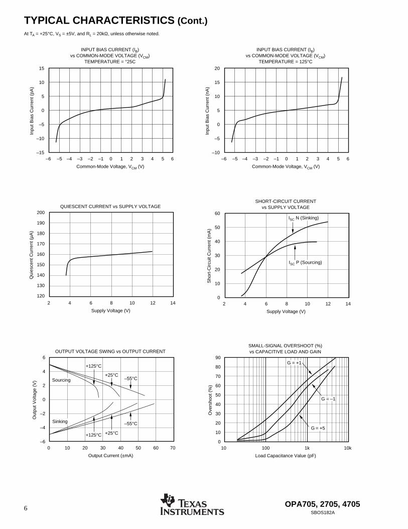
TYPICAL CHARACTERISTICS (Cont.)At TA = +25°C, VS = ±5V, and RL = 20kΩ, unless otherwise noted.
INPUT BIAS CURRENT (IB)vs COMMON-MODE VOLTAGE (VCM)
TEMPERATURE = °25C
–6
Inpu
t Bia
s C
urre
nt (
pA)
Common-Mode Voltage, VCM (V)
–5 –4 –3 –1 0–2 1 2 3 4 5 6
15
10
5
0
–5
–10
–15
QUIESCENT CURRENT vs SUPPLY VOLTAGE
2
Qui
esce
nt C
urre
nt (
µA)
Supply Voltage (V)
4 86 10 12 14
200
190
180
170
160
150
140
130
120
SHORT-CIRCUIT CURRENTvs SUPPLY VOLTAGE
2
Sho
rt-C
ircui
t Cur
rent
(m
A)
Supply Voltage (V)
4 86 10 12 14
60
50
40
30
20
10
0
ISC P (Sourcing)
ISC N (Sinking)
OUTPUT VOLTAGE SWING vs OUTPUT CURRENT
0
Out
put V
olta
ge (
V)
Output Current (±mA)
10 20 4030 50 60 70
6
4
2
0
–2
–4
–6
Sourcing
Sinking
+125°C +25°C
–55°C
+125°C
+25°C–55°C
SMALL-SIGNAL OVERSHOOT (%)vs CAPACITIVE LOAD AND GAIN
10
Ove
rsho
ot (
%)
Load Capacitance Value (pF)
100 1k 10k
90
80
70
60
50
40
30
20
10
0
G = +1
G = –1
G = +5
INPUT BIAS CURRENT (IB)vs COMMON-MODE VOLTAGE (VCM)
TEMPERATURE = 125°C
–6
Inpu
t Bia
s C
urre
nt (
nA)
Common-Mode Voltage, VCM (V)
–5 –4 –3 –1 0–2 1 2 3 4 5 6
20
15
10
5
0
–5
–10

OPA705, 2705, 4705 7SBOS182A
TYPICAL CHARACTERISTICS (Cont.)At TA = +25°C, VS = ±5V, and RL = 20kΩ, unless otherwise noted.
SETTLING TIME vs GAIN
1
Set
tling
Tim
e (µ
s)
Non-Inverting Gain (V/V)
10 100
100
90
80
70
60
50
40
30
20
10
0.1%
0.01%
VOS PRODUCTION DISTRIBUTION
Fre
quen
cy (
%)
Voltage Offset (mV)
–5.0
–4.5
–4.0
–3.5
–3.0
–2.5
–2.0
–1.5
–1.0
–0.5 0.1
0.5
1.0
1.5
2.0
2.5
3.0
3.5
4.0
4.5
5.0
25
20
15
10
5
0
VOS DRIFT PRODUCTION DISTRIBUTION
Fre
quen
cy (
%)
Voltage Offset (µV/°C)
≤ 30
≤ 24
≤ 18
≤ 12 ≤
6
< 0
< 6
< 1
2
< 1
8
< 2
4
< 3
0
≤ 27
≤ 21
≤ 15 ≤
9
≤ 3
< 3
< 9
< 1
5
< 2
1
< 2
7
> 3
0
25
20
15
10
5
0
SMALL SIGNAL STEP RESPONSE(G = +1V/V, RL = 20kΩ, CL = 100pF)
5µs/div
50m
V/d
iv
LARGE SIGNAL STEP RESPONSE(G = +1V/V, RL = 20kΩ, CL = 100pF)
10µs/div
1V/d
iv

OPA705, 2705, 47058SBOS182A
APPLICATIONS INFORMATIONOPA705 series op amps can operate on 160µA quiescentcurrent from a single (or split) supply in the range of 4V to12V (±2V to ±6V), making them highly versatile and easyto use. The OPA705 is unity-gain stable and offers 1MHzbandwidth and 0.6V/µs slew rate.
Rail-to-rail input and output swing helps maintain dynamicrange, especially in low supply applications. Figure 1 showsthe input and output waveforms for the OPA705 in unity-gain configuration. Operation is from a ±5V supply with a100kΩ load connected to VS/2. The input is a 10Vp-psinusoid. Output voltage is approximately 10Vp-p.
Power-supply pins should be bypassed with 1000pF ceramiccapacitors in parallel with 1µF tantalum capacitors.
OPERATING VOLTAGEOPA705 series op amps are fully specified and guaranteedfrom +4V to +12V over a temperature range of –40ºC to+85ºC. Parameters that vary significantly with operating volt-ages or temperature are shown in the Typical Characteristics.
RAIL-TO-RAIL INPUT
The input common-mode voltage range of the OPA705 seriesextends 300mV beyond the supply rails at room temperature.This is achieved with a complementary input stage—an N-channel input differential pair in parallel with a P-channeldifferential pair, as shown in Figure 2. The N-channel pair isactive for input voltages close to the positive rail, typically(V+) – 2.0V to 300mV above the positive supply, while the P-channel pair is on for inputs from 300mV below the negativesupply to approximately (V+) – 1.5V. There is a smalltransition region, typically (V+) – 2.0V to (V+) – 1.5V, inwhich both pairs are on. This 500mV transition region canvary ±100mV with process variation. Thus, the transitionregion (both stages on) can range from (V+) – 2.1V to (V+)– 1.4V on the low end, up to (V+) – 1.9V to (V+) – 1.6V onthe high end. Within the 500mV transition region PSRR,CMRR, offset voltage, and offset drift, and THD may varycompared to operation outside this region.
FIGURE 2. Simplified Schematic.
FIGURE 1. Rail-to-Rail Input and Output.
Input
Output (inverted on scope)
2.0V
/div
G = +1, VS = ±5V
200µs/div
VO
V–
V+
VIN+ VIN–

OPA705, 2705, 4705 9SBOS182A
RAIL-TO-RAIL OUTPUTA class AB output stage with common-source transistors isused to achieve rail-to-rail output. This output stage iscapable of driving 1kΩ loads connected to any point be-tween V+ and ground. For light resistive loads (> 100kΩ),the output voltage can swing to 40mV from the supply rail.With moderate resistive loads (20kΩ), the output can swingto within 75mV from the supply rails while maintaining highopen-loop gain (see the typical performance curve “OutputVoltage Swing vs Output Current”).
CAPACITIVE LOAD AND STABILITYThe OPA705 series op amps can drive up to 1000pF purecapacitive load. Increasing the gain enhances the amplifier’sability to drive greater capacitive loads (see the typicalperformance curve “Small Signal Overshoot vs CapacitiveLoad”).
One method of improving capacitive load drive in the unity-gain configuration is to insert a 10Ω to 20Ω resistor inside thefeedback loop, as shown in Figure 5. This reduces ringingwith large capacitive loads while maintaining DC accuracy.
FIGURE 5. Series Resistor in Unity-Gain Buffer Configura-tion Improves Capacitive Load Drive.
INPUT VOLTAGE
Device inputs are protected by ESD diodes that will conductif the input voltages exceed the power supplies by more thanapproximately 300mV. Momentary voltages greater than300mV beyond the power supply can be tolerated if thecurrent is limited to 10mA. This is easily accomplished withan input resistor, as shown in Figure 3. Many input signalsare inherently current-limited to less than 10mA; therefore,a limiting resistor is not always required. The OPA705features no phase inversion when the inputs extend beyondsupplies if the input current is limited, as seen in Figure 4.
FIGURE 4. OPA705—No Phase Inversion with InputsGreater than the Power-Supply Voltage.
FIGURE 3. Input Current Protection for Voltages Exceedingthe Supply Voltage.
2.0V
/div
VS = ±5.0V, VIN = 11Vp-p
20µs/div
APPLICATION CIRCUITS
The OPA705 series op amps are optimized for drivingmedium-speed sampling data converters. Figure 6 shows theOPA2705 in a dual-supply buffered reference configurationfor the DAC7644. The DAC7644 is a 16-bit, low-power,quad-voltage output converter. Small size makes the combi-nation ideal for automatic test equipment, data acquisitionsystems, and other low-power space-limited applications.
R
OPA70510mA max
+V
V–
VIN
VOUT
IOVERLOAD
RS20Ω
OPA705
CL RL
VIN
VOUT

OPA705, 2705, 470510SBOS182A
FIGURE 6. OPA705 as Dual Supply Configuration-Buffered References for the DAC7644.
NC
NC
NC
NC
VOUTA Sense
VOUTA
VREFL AB Sense
VREFL AB
VREFH AB
VREFH AB Sense
VOUTB Sense
VOUTB
48
47
46
45
44
43
42
41
40
39
38
37
DAC7644
500pF
+V
1/2OPA2705
Ref
1/2OPA2705
500pF
+2.5V
–V
V+
VOUT
VOUT
Ref–2.5V Negative
Reference
PositiveReference
V–

PACKAGE OPTION ADDENDUM
www.ti.com 11-Apr-2018
Addendum-Page 1
PACKAGING INFORMATION
Orderable Device Status(1)
Package Type PackageDrawing
Pins PackageQty
Eco Plan(2)
Lead/Ball Finish(6)
MSL Peak Temp(3)
Op Temp (°C) Device Marking(4/5)
Samples
OPA2705EA/250 ACTIVE VSSOP DGK 8 250 Green (RoHS& no Sb/Br)
CU NIPDAUAG Level-2-260C-1 YEAR -40 to 85 B05
OPA2705EA/250G4 ACTIVE VSSOP DGK 8 250 Green (RoHS& no Sb/Br)
CU NIPDAUAG Level-2-260C-1 YEAR -40 to 85 B05
OPA2705PA ACTIVE PDIP P 8 50 Green (RoHS& no Sb/Br)
CU NIPDAU | Call TI N / A for Pkg Type -40 to 85 OPA2705PA
OPA2705PAG4 ACTIVE PDIP P 8 50 Green (RoHS& no Sb/Br)
Call TI N / A for Pkg Type -40 to 85 OPA2705PA
OPA2705UA ACTIVE SOIC D 8 75 Green (RoHS& no Sb/Br)
CU NIPDAU Level-2-260C-1 YEAR -40 to 85 OPA2705UA
OPA2705UAG4 ACTIVE SOIC D 8 75 Green (RoHS& no Sb/Br)
CU NIPDAU Level-2-260C-1 YEAR -40 to 85 OPA2705UA
OPA4705EA/250 ACTIVE TSSOP PW 14 250 Green (RoHS& no Sb/Br)
CU NIPDAU Level-2-260C-1 YEAR -40 to 85 OPA4705EA
OPA4705EA/250G4 ACTIVE TSSOP PW 14 250 Green (RoHS& no Sb/Br)
CU NIPDAU Level-2-260C-1 YEAR -40 to 85 OPA4705EA
OPA4705EA/2K5 ACTIVE TSSOP PW 14 2500 Green (RoHS& no Sb/Br)
CU NIPDAU Level-2-260C-1 YEAR -40 to 85 OPA4705EA
OPA4705EA/2K5G4 ACTIVE TSSOP PW 14 2500 Green (RoHS& no Sb/Br)
CU NIPDAU Level-2-260C-1 YEAR -40 to 85 OPA4705EA
OPA705NA/250 ACTIVE SOT-23 DBV 5 250 Green (RoHS& no Sb/Br)
CU NIPDAU Level-2-260C-1 YEAR -40 to 85 A05
OPA705NA/250G4 ACTIVE SOT-23 DBV 5 250 Green (RoHS& no Sb/Br)
CU NIPDAU Level-2-260C-1 YEAR -40 to 85 A05
OPA705NA/3K ACTIVE SOT-23 DBV 5 3000 Green (RoHS& no Sb/Br)
CU NIPDAU Level-2-260C-1 YEAR -40 to 85 A05
OPA705PA ACTIVE PDIP P 8 50 Green (RoHS& no Sb/Br)
CU NIPDAU N / A for Pkg Type -40 to 85 OPA705PA
OPA705UA ACTIVE SOIC D 8 75 Green (RoHS& no Sb/Br)
CU NIPDAU Level-2-260C-1 YEAR -40 to 85 OPA705UA
(1) The marketing status values are defined as follows:ACTIVE: Product device recommended for new designs.LIFEBUY: TI has announced that the device will be discontinued, and a lifetime-buy period is in effect.NRND: Not recommended for new designs. Device is in production to support existing customers, but TI does not recommend using this part in a new design.

PACKAGE OPTION ADDENDUM
www.ti.com 11-Apr-2018
Addendum-Page 2
PREVIEW: Device has been announced but is not in production. Samples may or may not be available.OBSOLETE: TI has discontinued the production of the device.
(2) RoHS: TI defines "RoHS" to mean semiconductor products that are compliant with the current EU RoHS requirements for all 10 RoHS substances, including the requirement that RoHS substancedo not exceed 0.1% by weight in homogeneous materials. Where designed to be soldered at high temperatures, "RoHS" products are suitable for use in specified lead-free processes. TI mayreference these types of products as "Pb-Free".RoHS Exempt: TI defines "RoHS Exempt" to mean products that contain lead but are compliant with EU RoHS pursuant to a specific EU RoHS exemption.Green: TI defines "Green" to mean the content of Chlorine (Cl) and Bromine (Br) based flame retardants meet JS709B low halogen requirements of <=1000ppm threshold. Antimony trioxide basedflame retardants must also meet the <=1000ppm threshold requirement.
(3) MSL, Peak Temp. - The Moisture Sensitivity Level rating according to the JEDEC industry standard classifications, and peak solder temperature.
(4) There may be additional marking, which relates to the logo, the lot trace code information, or the environmental category on the device.
(5) Multiple Device Markings will be inside parentheses. Only one Device Marking contained in parentheses and separated by a "~" will appear on a device. If a line is indented then it is a continuationof the previous line and the two combined represent the entire Device Marking for that device.
(6) Lead/Ball Finish - Orderable Devices may have multiple material finish options. Finish options are separated by a vertical ruled line. Lead/Ball Finish values may wrap to two lines if the finishvalue exceeds the maximum column width.
Important Information and Disclaimer:The information provided on this page represents TI's knowledge and belief as of the date that it is provided. TI bases its knowledge and belief on informationprovided by third parties, and makes no representation or warranty as to the accuracy of such information. Efforts are underway to better integrate information from third parties. TI has taken andcontinues to take reasonable steps to provide representative and accurate information but may not have conducted destructive testing or chemical analysis on incoming materials and chemicals.TI and TI suppliers consider certain information to be proprietary, and thus CAS numbers and other limited information may not be available for release.
In no event shall TI's liability arising out of such information exceed the total purchase price of the TI part(s) at issue in this document sold by TI to Customer on an annual basis.

TAPE AND REEL INFORMATION
*All dimensions are nominal
Device PackageType
PackageDrawing
Pins SPQ ReelDiameter
(mm)
ReelWidth
W1 (mm)
A0(mm)
B0(mm)
K0(mm)
P1(mm)
W(mm)
Pin1Quadrant
OPA2705EA/250 VSSOP DGK 8 250 180.0 12.4 5.3 3.4 1.4 8.0 12.0 Q1
OPA4705EA/250 TSSOP PW 14 250 180.0 12.4 6.9 5.6 1.6 8.0 12.0 Q1
OPA4705EA/2K5 TSSOP PW 14 2500 330.0 12.4 6.9 5.6 1.6 8.0 12.0 Q1
OPA705NA/250 SOT-23 DBV 5 250 178.0 9.0 3.3 3.2 1.4 4.0 8.0 Q3
OPA705NA/3K SOT-23 DBV 5 3000 178.0 9.0 3.23 3.17 1.37 4.0 8.0 Q3
PACKAGE MATERIALS INFORMATION
www.ti.com 29-Jan-2014
Pack Materials-Page 1

*All dimensions are nominal
Device Package Type Package Drawing Pins SPQ Length (mm) Width (mm) Height (mm)
OPA2705EA/250 VSSOP DGK 8 250 210.0 185.0 35.0
OPA4705EA/250 TSSOP PW 14 250 210.0 185.0 35.0
OPA4705EA/2K5 TSSOP PW 14 2500 367.0 367.0 35.0
OPA705NA/250 SOT-23 DBV 5 250 180.0 180.0 18.0
OPA705NA/3K SOT-23 DBV 5 3000 180.0 180.0 18.0
PACKAGE MATERIALS INFORMATION
www.ti.com 29-Jan-2014
Pack Materials-Page 2

IMPORTANT NOTICE
Texas Instruments Incorporated (TI) reserves the right to make corrections, enhancements, improvements and other changes to itssemiconductor products and services per JESD46, latest issue, and to discontinue any product or service per JESD48, latest issue. Buyersshould obtain the latest relevant information before placing orders and should verify that such information is current and complete.TI’s published terms of sale for semiconductor products (http://www.ti.com/sc/docs/stdterms.htm) apply to the sale of packaged integratedcircuit products that TI has qualified and released to market. Additional terms may apply to the use or sale of other types of TI products andservices.Reproduction of significant portions of TI information in TI data sheets is permissible only if reproduction is without alteration and isaccompanied by all associated warranties, conditions, limitations, and notices. TI is not responsible or liable for such reproduceddocumentation. Information of third parties may be subject to additional restrictions. Resale of TI products or services with statementsdifferent from or beyond the parameters stated by TI for that product or service voids all express and any implied warranties for theassociated TI product or service and is an unfair and deceptive business practice. TI is not responsible or liable for any such statements.Buyers and others who are developing systems that incorporate TI products (collectively, “Designers”) understand and agree that Designersremain responsible for using their independent analysis, evaluation and judgment in designing their applications and that Designers havefull and exclusive responsibility to assure the safety of Designers' applications and compliance of their applications (and of all TI productsused in or for Designers’ applications) with all applicable regulations, laws and other applicable requirements. Designer represents that, withrespect to their applications, Designer has all the necessary expertise to create and implement safeguards that (1) anticipate dangerousconsequences of failures, (2) monitor failures and their consequences, and (3) lessen the likelihood of failures that might cause harm andtake appropriate actions. Designer agrees that prior to using or distributing any applications that include TI products, Designer willthoroughly test such applications and the functionality of such TI products as used in such applications.TI’s provision of technical, application or other design advice, quality characterization, reliability data or other services or information,including, but not limited to, reference designs and materials relating to evaluation modules, (collectively, “TI Resources”) are intended toassist designers who are developing applications that incorporate TI products; by downloading, accessing or using TI Resources in anyway, Designer (individually or, if Designer is acting on behalf of a company, Designer’s company) agrees to use any particular TI Resourcesolely for this purpose and subject to the terms of this Notice.TI’s provision of TI Resources does not expand or otherwise alter TI’s applicable published warranties or warranty disclaimers for TIproducts, and no additional obligations or liabilities arise from TI providing such TI Resources. TI reserves the right to make corrections,enhancements, improvements and other changes to its TI Resources. TI has not conducted any testing other than that specificallydescribed in the published documentation for a particular TI Resource.Designer is authorized to use, copy and modify any individual TI Resource only in connection with the development of applications thatinclude the TI product(s) identified in such TI Resource. NO OTHER LICENSE, EXPRESS OR IMPLIED, BY ESTOPPEL OR OTHERWISETO ANY OTHER TI INTELLECTUAL PROPERTY RIGHT, AND NO LICENSE TO ANY TECHNOLOGY OR INTELLECTUAL PROPERTYRIGHT OF TI OR ANY THIRD PARTY IS GRANTED HEREIN, including but not limited to any patent right, copyright, mask work right, orother intellectual property right relating to any combination, machine, or process in which TI products or services are used. Informationregarding or referencing third-party products or services does not constitute a license to use such products or services, or a warranty orendorsement thereof. Use of TI Resources may require a license from a third party under the patents or other intellectual property of thethird party, or a license from TI under the patents or other intellectual property of TI.TI RESOURCES ARE PROVIDED “AS IS” AND WITH ALL FAULTS. TI DISCLAIMS ALL OTHER WARRANTIES ORREPRESENTATIONS, EXPRESS OR IMPLIED, REGARDING RESOURCES OR USE THEREOF, INCLUDING BUT NOT LIMITED TOACCURACY OR COMPLETENESS, TITLE, ANY EPIDEMIC FAILURE WARRANTY AND ANY IMPLIED WARRANTIES OFMERCHANTABILITY, FITNESS FOR A PARTICULAR PURPOSE, AND NON-INFRINGEMENT OF ANY THIRD PARTY INTELLECTUALPROPERTY RIGHTS. TI SHALL NOT BE LIABLE FOR AND SHALL NOT DEFEND OR INDEMNIFY DESIGNER AGAINST ANY CLAIM,INCLUDING BUT NOT LIMITED TO ANY INFRINGEMENT CLAIM THAT RELATES TO OR IS BASED ON ANY COMBINATION OFPRODUCTS EVEN IF DESCRIBED IN TI RESOURCES OR OTHERWISE. IN NO EVENT SHALL TI BE LIABLE FOR ANY ACTUAL,DIRECT, SPECIAL, COLLATERAL, INDIRECT, PUNITIVE, INCIDENTAL, CONSEQUENTIAL OR EXEMPLARY DAMAGES INCONNECTION WITH OR ARISING OUT OF TI RESOURCES OR USE THEREOF, AND REGARDLESS OF WHETHER TI HAS BEENADVISED OF THE POSSIBILITY OF SUCH DAMAGES.Unless TI has explicitly designated an individual product as meeting the requirements of a particular industry standard (e.g., ISO/TS 16949and ISO 26262), TI is not responsible for any failure to meet such industry standard requirements.Where TI specifically promotes products as facilitating functional safety or as compliant with industry functional safety standards, suchproducts are intended to help enable customers to design and create their own applications that meet applicable functional safety standardsand requirements. Using products in an application does not by itself establish any safety features in the application. Designers mustensure compliance with safety-related requirements and standards applicable to their applications. Designer may not use any TI products inlife-critical medical equipment unless authorized officers of the parties have executed a special contract specifically governing such use.Life-critical medical equipment is medical equipment where failure of such equipment would cause serious bodily injury or death (e.g., lifesupport, pacemakers, defibrillators, heart pumps, neurostimulators, and implantables). Such equipment includes, without limitation, allmedical devices identified by the U.S. Food and Drug Administration as Class III devices and equivalent classifications outside the U.S.TI may expressly designate certain products as completing a particular qualification (e.g., Q100, Military Grade, or Enhanced Product).Designers agree that it has the necessary expertise to select the product with the appropriate qualification designation for their applicationsand that proper product selection is at Designers’ own risk. Designers are solely responsible for compliance with all legal and regulatoryrequirements in connection with such selection.Designer will fully indemnify TI and its representatives against any damages, costs, losses, and/or liabilities arising out of Designer’s non-compliance with the terms and provisions of this Notice.
Mailing Address: Texas Instruments, Post Office Box 655303, Dallas, Texas 75265Copyright © 2018, Texas Instruments Incorporated