EECC550 - Shaaban #1 Final Exam Review Winter 2003 2-19-2004 4 out of 5 or 6 questions 1Multicycle...
65
EECC550 - Shaaban EECC550 - Shaaban #1 Final Exam Review Winter 2003 2-1 4 out of 5 or 6 questions 1 Multicycle CPU performance vs. ideal pipeline performance 2 Given MIPS code, MIPS pipeline (similar to questions 2, 3 of HW#4) – Performance of code as is on a given CPU – Schedule the code to reduce stalls + resulting performance 3 Given a series of word memory address references, cache capacity and organization: (similar to chapter 7 exercises 7, 8 , 20, 21 , 22) – Find Hits/misses, Hit rate, Final content of cache 4 Pipelined CPU performance with non-ideal memory and unified or split cache – Find AMAT, CPI, performance … 5 For a cache level with given characteristics find: – Address fields, mapping function, storage requirements etc. 6 Performance comparison of non-ideal pipelined CPUs using non ideal memory,, Cache, code and main memory penalty: – Desired performance maybe given: Find missing parameter EECC550 Exam EECC550 Exam Review Review
-
date post
22-Dec-2015 -
Category
Documents
-
view
236 -
download
1
Transcript of EECC550 - Shaaban #1 Final Exam Review Winter 2003 2-19-2004 4 out of 5 or 6 questions 1Multicycle...
EECC550 - ShaabanEECC550 - Shaaban#1 Final Exam Review Winter 2003 2-19-2004
4 out of 5 or 6 questions
1 Multicycle CPU performance vs. ideal pipeline performance
2 Given MIPS code, MIPS pipeline (similar to questions 2, 3 of HW#4)
– Performance of code as is on a given CPU– Schedule the code to reduce stalls + resulting performance
3 Given a series of word memory address references, cache capacity and organization: (similar to chapter 7 exercises 7, 8 , 20, 21 , 22)
– Find Hits/misses, Hit rate, Final content of cache
4 Pipelined CPU performance with non-ideal memory and unified or split cache
– Find AMAT, CPI, performance …
5 For a cache level with given characteristics find:– Address fields, mapping function, storage requirements etc.
6 Performance comparison of non-ideal pipelined CPUs using non ideal memory,, Cache, code and main memory penalty:
– Desired performance maybe given: Find missing parameter
EECC550 Exam ReviewEECC550 Exam Review
EECC550 - ShaabanEECC550 - Shaaban#2 Final Exam Review Winter 2003 2-19-2004
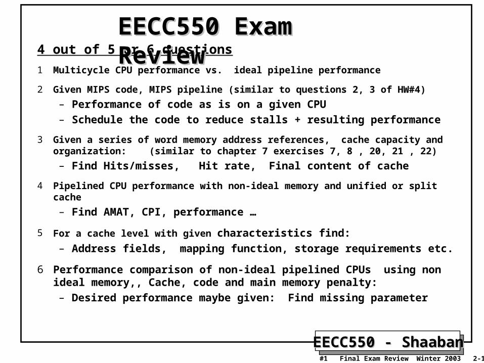
Multi-cycle Datapath (Our Version)Multi-cycle Datapath (Our Version)
PC
Nex
t P
C
Ope
rand
Fet
ch
Ext
ALU Reg
. F
ile
Mem
Acc
ess
Dat
aM
em
Inst
ruct
ion
Fet
ch
Res
ult
Sto
re
AL
Uct
r
Reg
Dst
AL
US
rc
Ext
Op
nPC
_sel
Reg
Wr
Mem
Wr
Mem
Rd
IR
A
B
R
M
RegFile
Mem
ToR
eg
Equ
al
Registers added:
IR: Instruction registerA, B: Two registers to hold operands read from register file.R: or ALUOut, holds the output of the ALUM: or Memory data register (MDR) to hold data read from data memory

EECC550 - ShaabanEECC550 - Shaaban#3 Final Exam Review Winter 2003 2-19-2004
Operations In Each CycleOperations In Each Cycle
Instruction Fetch
Instruction Decode
Execution
Memory
WriteBack
R-Type
IR Mem[PC]
A R[rs]
B R[rt]
R A + B
R[rd] R
PC PC + 4
Logic Immediate
IR Mem[PC]
A R[rs]
R A OR ZeroExt[imm16]
R[rt] R
PC PC + 4
Load
IR Mem[PC]
A R[rs]
R A + SignEx(Im16)
M Mem[R]
R[rd] M
PC PC + 4
Store
IR Mem[PC]
A R[rs]
B R[rt]
R A + SignEx(Im16)
Mem[R] B
PC PC + 4
Branch
IR Mem[PC]
A R[rs]
B R[rt]
If Equal = 1
PC PC + 4 +
(SignExt(imm16) x4)
else
PC PC + 4
IF
ID
EX
MEM
WB

EECC550 - ShaabanEECC550 - Shaaban#4 Final Exam Review Winter 2003 2-19-2004
Multi-cycle Datapath Instruction CPIMulti-cycle Datapath Instruction CPI• R-Type/Immediate: Require four cycles, CPI =4
– IF, ID, EX, WB
• Loads: Require five cycles, CPI = 5– IF, ID, EX, MEM, WB
• Stores: Require four cycles, CPI = 4– IF, ID, EX, MEM
• Branches: Require three cycles, CPI = 3– IF, ID, EX
• Average program 3 CPI 5 depending on program profile (instruction mix).

EECC550 - ShaabanEECC550 - Shaaban#5 Final Exam Review Winter 2003 2-19-2004
MIPS Multi-cycle Datapath MIPS Multi-cycle Datapath Performance EvaluationPerformance Evaluation
• What is the average CPI?– State diagram gives CPI for each instruction type.
– Workload (program) below gives frequency of each type.
Type CPIi for type Frequency CPIi x freqIi
Arith/Logic 4 40% 1.6
Load 5 30% 1.5
Store 4 10% 0.4
branch 3 20% 0.6
Average CPI: 4.1
Better than CPI = 5 if all instructions took the same number of clock cycles (5).

EECC550 - ShaabanEECC550 - Shaaban#6 Final Exam Review Winter 2003 2-19-2004
Instruction PipeliningInstruction Pipelining• Instruction pipelining is a CPU implementation technique where multiple
operations on a number of instructions are overlapped.– For Example: The next instruction is fetched in the next cycle without
waiting for the current instruction to complete.• An instruction execution pipeline involves a number of steps, where each step
completes one part of an instruction.• Each step is called a pipeline stage or a pipeline segment.• The stages or steps are connected one to the next to form a pipeline --
instructions enter at one end and progress through the stages and exit at the other end when completed.
• Instruction Pipeline Throughput : The instruction completion rate of the pipeline and is determined by how often an instruction exists the pipeline.
• The time to move an instruction one step down the pipeline is is equal to the machine (CPU) cycle and is determined by the stage with the longest processing delay.
• Instruction Pipeline Latency: The time required to complete an instruction:
= Cycle time x Number of pipeline stages

EECC550 - ShaabanEECC550 - Shaaban#7 Final Exam Review Winter 2003 2-19-2004
Pipelining: Design GoalsPipelining: Design Goals• The length of the machine clock cycle is determined by the time
required for the slowest pipeline stage.
• An important pipeline design consideration is to balance the length of each pipeline stage.
• If all stages are perfectly balanced, then the time per instruction on a pipelined machine (assuming ideal conditions with no stalls):
Time per instruction on unpipelined machine Number of pipe stages
• Under these ideal conditions:– Speedup from pipelining = the number of pipeline stages = k
– Goal: One instruction is completed every cycle: CPI = 1 .

EECC550 - ShaabanEECC550 - Shaaban#8 Final Exam Review Winter 2003 2-19-2004
Ideal pipeline operation without any stall cycles
Ideal Pipelined Instruction Ideal Pipelined Instruction Processing Timing RepresentationProcessing Timing Representation
Clock cycle Number Time in clock cycles Instruction Number 1 2 3 4 5 6 7 8 9
Instruction I IF ID EX MEM WB
Instruction I+1 IF ID EX MEM WB
Instruction I+2 IF ID EX MEM WB
Instruction I+3 IF ID EX MEM WB
Instruction I +4 IF ID EX MEM WB
Time to fill the pipeline
5 Pipeline Stages:
IF = Instruction Fetch
ID = Instruction Decode
EX = Execution
MEM = Memory Access
WB = Write Back
First instruction, ICompleted
Instruction, I+4 completed
Pipeline Fill Cycles: No instructions completed yetNumber of fill cycles = Number of pipeline stages - 1 Here 5 - 1 = 4 fill cyclesIdeal pipeline operation: After fill cycles, one instruction is completed per cycle giving the ideal pipeline CPI = 1 (ignoring fill cycles)

EECC550 - ShaabanEECC550 - Shaaban#9 Final Exam Review Winter 2003 2-19-2004
Ideal Pipelined Instruction Processing Ideal Pipelined Instruction Processing RepresentationRepresentation
IF ID EX MEM WB
IF ID EX MEM WB
IF ID EX MEM WB
IF ID EX MEM WB
IF ID EX MEM WB
IF ID EX MEM WBProgram Flow
Time
Here 5 pipeline stages or steps
Number of pipeline fill cycles = Number of stages - 1 Here 5 -1 = 4After fill cycles: One instruction is completed every cycle
Pipeline Fill cycles = 5 -1 = 4
I1
I2
I3
I4
I5
I6
1 2 3 4 5 6 7 8 9 10
Ideal pipeline operation without any stall cycles

EECC550 - ShaabanEECC550 - Shaaban#10 Final Exam Review Winter 2003 2-19-2004
Single Cycle, Multi-Cycle, Vs. PipelineSingle Cycle, Multi-Cycle, Vs. Pipeline
Clk
Cycle 1
Multiple Cycle Implementation:
IF ID EX MEM WB
Cycle 2 Cycle 3 Cycle 4 Cycle 5 Cycle 6 Cycle 7 Cycle 8 Cycle 9 Cycle 10
IF ID EX MEM
Load Store
Clk
Single Cycle Implementation:
Load Store Waste
IF
R-type
Load IF ID EX MEM WB
Pipeline Implementation:
IF ID EX MEM WBStore
IF ID EX MEM WBR-type
Cycle 1 Cycle 2
8 ns
2ns
EECC550 - ShaabanEECC550 - Shaaban#11 Final Exam Review Winter 2003 2-19-2004
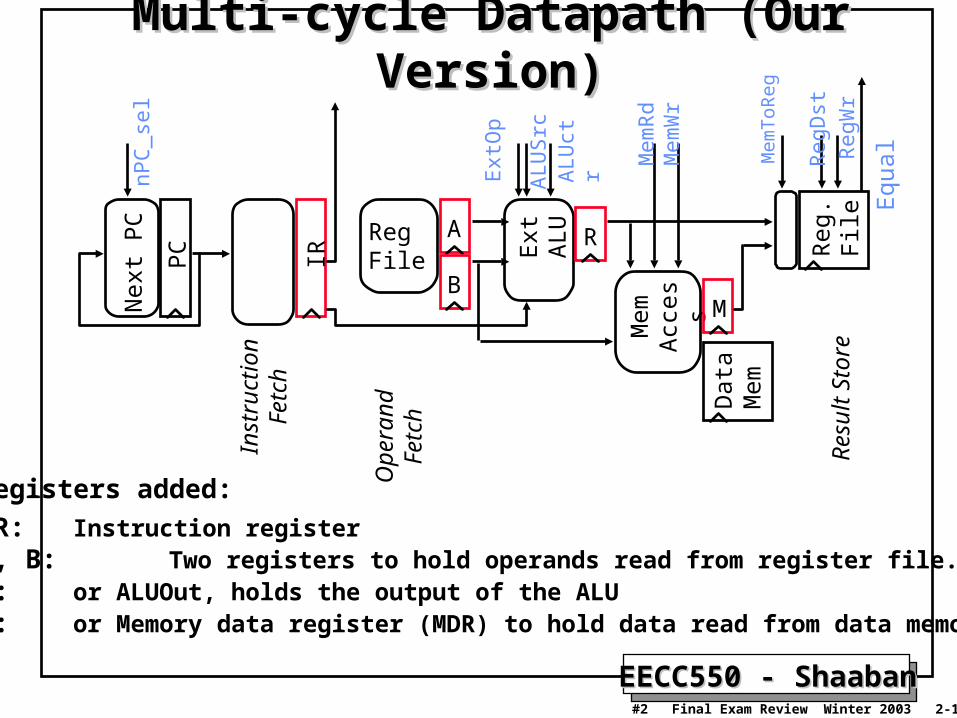
For 1000 instructions, execution time:
• Single Cycle Machine:
– 8 ns/cycle x 1 CPI x 1000 inst = 8000 ns
• Multi-cycle Machine:
– 2 ns/cycle x 4.6 CPI (due to inst mix) x 1000 inst = 9200 ns
• Ideal pipelined machine, 5-stages:
– 2 ns/cycle x (1 CPI x 1000 inst + 4 cycle fill) = 2008 ns
Single Cycle, Multi-Cycle, Pipeline:Single Cycle, Multi-Cycle, Pipeline:Performance Comparison ExamplePerformance Comparison Example

EECC550 - ShaabanEECC550 - Shaaban#12 Final Exam Review Winter 2003 2-19-2004
A Pipelined DatapathA Pipelined Datapath
Instructionmemory
Address
4
32
0
Add Addresult
Shiftleft 2
Inst
ruct
ion
IF/ID EX/MEM MEM/WB
Mux
0
1
Add
PC
0
Address
Writedata
Mux
1Registers
Readdata 1
Readdata 2
Readregister 1
Readregister 2
16Sign
extend
Writeregister
Writedata
Readdata
Datamemory
1
ALUresult
Mux
ALUZero
ID/EX
IF ID EX MEM WBInstruction Fetch Instruction Decode Execution Memory Write Back

EECC550 - ShaabanEECC550 - Shaaban#13 Final Exam Review Winter 2003 2-19-2004
Read/Write Access To Register BankRead/Write Access To Register Bank
IM Reg DM Reg
IM Reg DM Reg
CC 1 CC 2 CC 3 CC 4 CC 5 CC 6
Time (in clock cycles)
lw $10, 20($1)
Programexecutionorder(in instructions)
sub $11, $2, $3
ALU
ALU
• Two instructions need to access the register bank in the same cycle:– One instruction to read operands in its instruction decode (ID) cycle.– The other instruction to write to a destination register in its Write Back
(WB) cycle.• This represents a potential hardware conflict over access to the register bank.• Solution: Coordinate register reads and write in the same cycle as follows:
• Register write in Write Back WB cycle occur in the first half of the cycle. (indicated here by the dark shading of the first half of the WB cycle)
• Operand register reads in Instruction Decode ID cycle occur in the second half of the cycle (indicated here by the dark shading of the second half of the cycle)

EECC550 - ShaabanEECC550 - Shaaban#14 Final Exam Review Winter 2003 2-19-2004
Pipeline ControlPipeline Control• Pass needed control signals along from one stage to the next as the instruction travels through the
pipeline just like the data
Execution/Address Calculation stage control lines
Memory access stage control lines
Write-back stage control
lines
InstructionReg Dst
ALU Op1
ALU Op0
ALU Src Branch
Mem Read
Mem Write
Reg write
Mem to Reg
R-format 1 1 0 0 0 0 0 1 0lw 0 0 0 1 0 1 0 1 1sw X 0 0 1 0 0 1 0 Xbeq X 0 1 0 1 0 0 0 X
Control
EX
M
WB
M
WB
WB
IF/ID ID/EX EX/MEM MEM/WB
Instruction

EECC550 - ShaabanEECC550 - Shaaban#15 Final Exam Review Winter 2003 2-19-2004
Pipelined Datapath with Control AddedPipelined Datapath with Control Added
PC
Instructionmemory
Inst
ruct
ion
Add
Instruction[20– 16]
Me
mto
Re
g
ALUOp
Branch
RegDst
ALUSrc
4
16 32Instruction[15– 0]
0
0
Mux
0
1
Add Addresult
RegistersWriteregister
Writedata
Readdata 1
Readdata 2
Readregister 1
Readregister 2
Signextend
Mux
1
ALUresult
Zero
Writedata
Readdata
Mux
1
ALUcontrol
Shiftleft 2
Re
gWrit
e
MemRead
Control
ALU
Instruction[15– 11]
6
EX
M
WB
M
WB
WBIF/ID
PCSrc
ID/EX
EX/MEM
MEM/WB
Mux
0
1
Me
mW
rite
AddressData
memory
Address
Target address of branch determined in MEM

EECC550 - ShaabanEECC550 - Shaaban#16 Final Exam Review Winter 2003 2-19-2004
Basic Performance Issues In Basic Performance Issues In PipeliningPipelining• Pipelining increases the CPU instruction throughput:
The number of instructions completed per unit time. Under ideal conditions (i.e. No stall cycles):
– Pipelined CPU instruction throughput is one instruction completed per machine cycle, or CPI = 1 (ignoring pipeline fill cycles)
• Pipelining does not reduce the execution time of an individual instruction: The time needed to complete all processing steps of an instruction (also called instruction completion latency).
– It usually slightly increases the execution time of individual instructions over unpipelined CPU implementations due to:
• The increased control overhead of the pipeline and pipeline stage registers delays +
• Every instruction goes though every stage in the pipeline even if the stage is not needed. (i.e MEM pipeline stage in the case of R-Type instructions)

EECC550 - ShaabanEECC550 - Shaaban#17 Final Exam Review Winter 2003 2-19-2004
Pipelining Performance ExamplePipelining Performance Example• Example: For an unpipelined multicycle CPU:
– Clock cycle = 10ns, 4 cycles for ALU operations and branches and 5 cycles for memory operations with instruction frequencies of 40%, 20% and 40%, respectively.
– If pipelining adds 1ns to the CPU clock cycle then the speedup in instruction execution from pipelining is:
Non-pipelined Average execution time/instruction = Clock cycle x Average CPI
= 10 ns x ((40% + 20%) x 4 + 40%x 5) = 10 ns x 4.4 = 44 ns
In the pipelined CPU implementation, ideal CPI = 1
Pipelined execution time/instruction = Clock cycle x CPI
= (10 ns + 1 ns) x 1 = 11 ns x 1 = 11 ns
Speedup from pipelining = Time Per Instruction time unpipelined
Time per Instruction time pipelined
= 44 ns / 11 ns = 4 times faster
EECC550 - ShaabanEECC550 - Shaaban#18 Final Exam Review Winter 2003 2-19-2004
Pipeline HazardsPipeline Hazards• Hazards are situations in pipelining which prevent the next
instruction in the instruction stream from executing during the designated clock cycle resulting in one or more stall cycles.
• Hazards reduce the ideal speedup gained from pipelining and are classified into three classes:
– Structural hazards: Arise from hardware resource conflicts when the available hardware cannot support all possible combinations of instructions.
– Data hazards: Arise when an instruction depends on the results of a previous instruction in a way that is exposed by the overlapping of instructions in the pipeline.
– Control hazards: Arise from the pipelining of conditional branches and other instructions that change the PC.

EECC550 - ShaabanEECC550 - Shaaban#19 Final Exam Review Winter 2003 2-19-2004
Structural (or Hardware) HazardsStructural (or Hardware) Hazards• In pipelined machines overlapped instruction execution
requires pipelining of functional units and duplication of resources to allow all possible combinations of instructions in the pipeline.
• If a resource conflict arises due to a hardware resource being required by more than one instruction in a single cycle, and one or more such instructions cannot be accommodated, then a structural hazard has occurred, for example:– When a pipelined machine has a shared single-memory for both
data and instructions. stall the pipeline for one cycle for memory data access

EECC550 - ShaabanEECC550 - Shaaban#20 Final Exam Review Winter 2003 2-19-2004
Structural hazard Example: Single Memory For Instructions & Data
Mem
Instr.
Order
Time (clock cycles)
Load
Instr 1
Instr 2
Instr 3
Instr 4A
LUMem Reg Mem Reg
AL
UMem Reg Mem Reg
AL
UMem Reg Mem Reg
AL
UReg Mem Reg
AL
UMem Reg Mem Reg
Detection is easy in this case (right half highlight means read, left half write)

EECC550 - ShaabanEECC550 - Shaaban#21 Final Exam Review Winter 2003 2-19-2004
Data HazardsData Hazards• Data hazards occur when the pipeline changes the order of
read/write accesses to instruction operands in such a way that the resulting access order differs from the original sequential instruction operand access order of the unpipelined CPU resulting in incorrect execution.
• Data hazards may require one or more instructions to be stalled in the pipeline to ensure correct execution.
• Example:sub $2, $1, $3and $12, $2, $5or $13, $6, $2add $14, $2, $2sw $15, 100($2)
– All the instructions after the sub instruction use its result data in register $2– As part of pipelining, these instruction are started before sub is completed:
• Due to this data hazard instructions need to be stalled for correct execution.(As shown next)

EECC550 - ShaabanEECC550 - Shaaban#22 Final Exam Review Winter 2003 2-19-2004
Data Hazards ExampleData Hazards Example• Problem with starting next instruction before first is finished
– Data dependencies here that “go backward in time” create data hazards.
sub $2, $1, $3and $12, $2, $5or $13, $6, $2add $14, $2, $2sw $15, 100($2)
IM Reg
IM Reg
CC 1 CC 2 CC 3 CC 4 CC 5 CC 6
Time (in clock cycles)
sub $2, $1, $3
Programexecutionorder(in instructions)
and $12, $2, $5
IM Reg DM Reg
IM DM Reg
IM DM Reg
CC 7 CC 8 CC 9
10 10 10 10 10/– 20 – 20 – 20 – 20 – 20
or $13, $6, $2
add $14, $2, $2
sw $15, 100($2)
Value of register $2:
DM Reg
Reg
Reg
Reg
DM

EECC550 - ShaabanEECC550 - Shaaban#23 Final Exam Review Winter 2003 2-19-2004
Data Hazard Resolution: Stall Cycles Data Hazard Resolution: Stall Cycles Stall the pipeline by a number of cycles.The control unit must detect the need to insert stall cycles.
In this case two stall cycles are needed.
IM Reg
IM
CC 1 CC 2 CC 3 CC 4 CC 5 CC 6
Time (in clock cycles)
sub $2, $1, $3
Programexecutionorder(in instructions)
and $12, $2, $5
CC 7 CC 8
10 10 10 10 10/– 20 – 20 – 20 – 20
CC 9
– 20
or $13, $6, $2
add $14, $2, $2
sw $15, 100($2)
Value of register $2:
DM Reg
Reg
IM Reg DM Reg
IM DM Reg
IM DM Reg
Reg
Reg
Reg
DMSTALL STALL
CC 10
– 20
CC 11
– 20
STALL STALL

EECC550 - ShaabanEECC550 - Shaaban#24 Final Exam Review Winter 2003 2-19-2004
Performance of Pipelines with StallsPerformance of Pipelines with Stalls• Hazard conditions in pipelines may make it necessary to stall the
pipeline by a number of cycles degrading performance from the ideal pipelined CPU CPI of 1.
CPI pipelined = Ideal CPI + Pipeline stall clock cycles per instruction
= 1 + Pipeline stall clock cycles per instruction
• If pipelining overhead is ignored and we assume that the stages are perfectly balanced then speedup from pipelining is given by:
Speedup = CPI unpipelined / CPI pipelined
= CPI unpipelined / (1 + Pipeline stall cycles per instruction)
• When all instructions in the multicycle CPU take the same number of cycles equal to the number of pipeline stages then:
Speedup = Pipeline depth / (1 + Pipeline stall cycles per instruction)

EECC550 - ShaabanEECC550 - Shaaban#25 Final Exam Review Winter 2003 2-19-2004
• Observation: Why not use temporary results produced by memory/ALU and not
wait for them to be written back in the register bank.
• Forwarding is a hardware-based technique (also called register bypassing or short-circuiting) used to eliminate or minimize data hazard stalls that makes use of this observation.
• Using forwarding hardware, the result of an instruction is copied directly from where it is produced (ALU, memory read port etc.), to where subsequent instructions need it (ALU input register, memory write port etc.)
Data Hazard Resolution: Forwarding Data Hazard Resolution: Forwarding

EECC550 - ShaabanEECC550 - Shaaban#26 Final Exam Review Winter 2003 2-19-2004
Pipelined Datapath With ForwardingPipelined Datapath With Forwarding
PCInstruction
memory
Registers
Mux
Mux
Control
ALU
EX
M
WB
M
WB
WB
ID/EX
EX/MEM
MEM/WB
Datamemory
Mux
Forwardingunit
IF/ID
Inst
ruct
ion
Mux
RdEX/MEM.RegisterRd
MEM/WB.RegisterRd
Rt
Rt
Rs
IF/ID.RegisterRd
IF/ID.RegisterRt
IF/ID.RegisterRt
IF/ID.RegisterRs

EECC550 - ShaabanEECC550 - Shaaban#27 Final Exam Review Winter 2003 2-19-2004
Data Hazard Example With ForwardingData Hazard Example With Forwarding
IM Reg
IM Reg
CC 1 CC 2 CC 3 CC 4 CC 5 CC 6
Time (in clock cycles)
sub $2, $1, $3
Programexecution order(in instructions)
and $12, $2, $5
IM Reg DM Reg
IM DM Reg
IM DM Reg
CC 7 CC 8 CC 9
10 10 10 10 10/– 20 – 20 – 20 – 20 – 20
or $13, $6, $2
add $14, $2, $2
sw $15, 100($2)
Value of register $2 :
DM Reg
Reg
Reg
Reg
X X X – 20 X X X X XValue of EX/MEM :X X X X – 20 X X X XValue of MEM/WB :
DM

EECC550 - ShaabanEECC550 - Shaaban#28 Final Exam Review Winter 2003 2-19-2004
A Data Hazard Requiring A StallA Data Hazard Requiring A Stall
Reg
IM
Reg
Reg
IM
CC 1 CC 2 CC 3 CC 4 CC 5 CC 6
Time (in clock cycles)
lw $2, 20($1)
Programexecutionorder(in instructions)
and $4, $2, $5
IM Reg DM Reg
IM DM Reg
IM DM Reg
CC 7 CC 8 CC 9
or $8, $2, $6
add $9, $4, $2
slt $1, $6, $7
DM Reg
Reg
Reg
DM
A load followed by an R-type instruction that uses the loaded value
Even with forwarding in place a stall cycle is neededThis condition must be detected by hardware

EECC550 - ShaabanEECC550 - Shaaban#29 Final Exam Review Winter 2003 2-19-2004
A Data Hazard Requiring A StallA Data Hazard Requiring A StallA load followed by an R-type instruction that uses the loaded valueresults in a single stall cycle even with forwarding as shown:
• We can stall the pipeline by keeping all instructions following the “lw” instruction in the same pipeline stage for one cycle
lw $2, 20($1)
Programexecutionorder(in instructions)
and $4, $2, $5
or $8, $2, $6
add $9, $4, $2
slt $1, $6, $7
Reg
IM
Reg
Reg
IM DM
CC 1 CC 2 CC 3 CC 4 CC 5 CC 6Time (in clock cycles)
IM Reg DM RegIM
IM DM Reg
IM DM Reg
CC 7 CC 8 CC 9 CC 10
DM Reg
RegReg
Reg
bubble
A stall cycle
Stall one cycle then, forward data of “lw” instruction to “and” instruction
EECC550 - ShaabanEECC550 - Shaaban#30 Final Exam Review Winter 2003 2-19-2004
Compiler Scheduling ExampleCompiler Scheduling Example• Reorder the instructions to avoid as many pipeline stalls as possible:
lw $15, 0($2)lw $16, 4($2)add $14, $5, $16sw $16, 4($2)
• The data hazard occurs on register $16 between the second lw and the add resulting in a stall cycle
• With forwarding we need to find only one independent instructions to place between them, swapping the lw instructions works:
lw $16, 4($2)lw $15, 0($2)nopadd $14, $5, $16 sw $16, 4($2)
• Without forwarding we need two independent instructions to place between them, so in addition a nop is added.
lw $16, 4($2)lw $15, 0($2)add $14, $5, $16sw $16, 4($2)

EECC550 - ShaabanEECC550 - Shaaban#31 Final Exam Review Winter 2003 2-19-2004
Datapath With Hazard Detection UnitDatapath With Hazard Detection Unit
PCInstruction
memory
Registers
Mux
Mux
Mux
Control
ALU
EX
M
WB
M
WB
WB
ID/EX
EX/MEM
MEM/WB
Datamemory
Mux
Hazarddetection
unit
Forwardingunit
0
Mux
IF/ID
Inst
ruct
ion
ID/EX.MemReadIF
/IDW
rite
PC
Writ
e
ID/EX.RegisterRt
IF/ID.RegisterRd
IF/ID.RegisterRtIF/ID.RegisterRt
IF/ID.RegisterRs
RtRs
Rd
Rt EX/MEM.RegisterRd
MEM/WB.RegisterRd
A load followed by an instruction that uses the loaded value is detectedand a stall cycle is inserted.

EECC550 - ShaabanEECC550 - Shaaban#32 Final Exam Review Winter 2003 2-19-2004
Control HazardsControl Hazards• When a conditional branch is executed it may change the PC and,
without any special measures, leads to stalling the pipeline for a number of cycles until the branch condition is known (branch is resolved).
– Otherwise the PC may not be correct when needed in IF
• In current MIPS pipeline, the conditional branch is resolved in stage 4 (MEM stage) resulting in three stall cycles as shown below:
Branch instruction IF ID EX MEM WBBranch successor stall stall stall IF ID EX MEM WBBranch successor + 1 IF ID EX MEM WB Branch successor + 2 IF ID EX MEMBranch successor + 3 IF ID EXBranch successor + 4 IF IDBranch successor + 5 IF
Assuming we stall or flush the pipeline on a branch instruction: Three clock cycles are wasted for every branch for current MIPS pipeline
Branch Penalty = stage number where branch is resolved - 1 here Branch Penalty = 4 - 1 = 3 Cycles
3 stall cycles

EECC550 - ShaabanEECC550 - Shaaban#33 Final Exam Review Winter 2003 2-19-2004
Basic Branch Handling in PipelinesBasic Branch Handling in Pipelines 1 One scheme discussed earlier is to always stall ( flush or freeze) the pipeline whenever a
conditional branch is decoded by holding or deleting any instructions in the pipeline until the branch destination is known (zero pipeline registers, control lines).
Pipeline stall cycles from branches = frequency of branches X branch penalty
• Ex: Branch frequency = 20% branch penalty = 3 cycles
CPI = 1 + .2 x 3 = 1.6
2 Another method is to assume or predict that the branch is not taken where the state of the machine is not changed until the branch outcome is definitely known. Execution here continues with the next instruction; stall occurs here when the branch is taken.
Pipeline stall cycles from branches = frequency of taken branches X branch penalty
• Ex: Branch frequency = 20% of which 45% are taken branch penalty = 3 cycles
CPI = 1 + .2 x .45 x 3 = 1.27

EECC550 - ShaabanEECC550 - Shaaban#34 Final Exam Review Winter 2003 2-19-2004
Control Hazards: ExampleControl Hazards: Example• Three other instructions are in the pipeline before branch instruction target decision is made when BEQ is in MEM stage.
• In the above diagram, we are predicting “branch not taken”– Need to add hardware for flushing the three following instructions if we are wrong losing three cycles.
Reg
Reg
CC 1
Time (in clock cycles)
40 beq $1, $3, 7
Programexecutionorder(in instructions)
IM Reg
IM DM
IM DM
IM DM
DM
DM Reg
Reg Reg
Reg
Reg
RegIM
44 and $12, $2, $5
48 or $13, $6, $2
52 add $14, $2, $2
72 lw $4, 50($7)
CC 2 CC 3 CC 4 CC 5 CC 6 CC 7 CC 8 CC 9
Reg

EECC550 - ShaabanEECC550 - Shaaban#35 Final Exam Review Winter 2003 2-19-2004
Reducing Delay (Penalty) of Taken BranchesReducing Delay (Penalty) of Taken Branches• So far: Next PC of a branch known or resolved in MEM stage: Costs three lost cycles if the branch is
taken.• If next PC of a branch is known or resolved in EX stage, one cycle is saved.• Branch address calculation can be moved to ID stage (stage 2) using a register comparator, costing only
one cycle if branch is taken as shown below. Branch Penalty = stage 2 -1 = 1 cycle
PCInstruction
memory
4
Registers
Mux
Mux
Mux
ALU
EX
M
WB
M
WB
WB
ID/EX
0
EX/MEM
MEM/WB
Datamemory
Mux
Hazarddetection
unit
Forwardingunit
IF.Flush
IF/ID
Signextend
Control
Mux
=
Shiftleft 2
Mux
Here the branch is resolved in ID stage(stage 2) Thus branch penalty if taken = 2 - 1 = 1 cycle
IF ID MEMEX WB

EECC550 - ShaabanEECC550 - Shaaban#36 Final Exam Review Winter 2003 2-19-2004
Reduction of Branch Penalties:Reduction of Branch Penalties:Delayed BranchDelayed Branch
• When delayed branch is used in an ISA, the branch is delayed by n cycles (or instructions), following this execution pattern:
conditional branch instruction
sequential successor1
sequential successor2
…….. sequential successorn
branch target if taken
• The sequential successor instructions are said to be in the branch delay slots. These instructions are executed whether or not the branch is taken.
• In Practice, all ISAs that utilize delayed branching including MIPS utilize a single instruction branch delay slot.
– The job of the compiler is to make the successor instruction in the delay slot a valid and useful instruction.

EECC550 - ShaabanEECC550 - Shaaban#37 Final Exam Review Winter 2003 2-19-2004
• Schedule the following MIPS code for the pipelined MIPS CPU with forwarding and reduced branch delay using a single branch delay slot to minimize stall cycles:
loop: lw $1,0($2) # $1 array element
add $1, $1, $3 # add constant in $3
sw $1,0($2) # store result array element
addi $2, $2, -4 # decrement address by 4
bne $2, $4, loop # branch if $2 != $4
• Assuming the initial value of $2 = $4 + 40
(i.e it loops 10 times)
– What is the CPI and total number of cycles needed to run the code with and without scheduling?
Compiler Instruction Scheduling ExampleCompiler Instruction Scheduling ExampleWith Branch Delay SlotWith Branch Delay Slot

EECC550 - ShaabanEECC550 - Shaaban#38 Final Exam Review Winter 2003 2-19-2004
• Without compiler scheduling
loop: lw $1,0($2)
Stall
add $1, $1, $3
sw $1,0($2)addi $2, $2, -4
Stall
bne $2, $4, loop
StallIgnoring the initial 4 cycles to fill the
pipeline: Each iteration takes = 8 cycles
CPI = 8/5 = 1.6
Total cycles = 8 x 10 = 80 cycles
Compiler Instruction Scheduling ExampleCompiler Instruction Scheduling Example(With Branch Delay Slot)(With Branch Delay Slot)
• With compiler scheduling
loop: lw $1,0($2)
addi $2, $2, -4
add $1, $1, $3
bne $2, $4, loop
sw $1, 4($2)
Ignoring the initial 4 cycles to fill the
pipeline: Each iteration takes = 5 cycles
CPI = 5/5 = 1
Total cycles = 5 x 10 = 50 cycles
Speedup = 80/ 50 = 1.6
Moveto branch delay slot
Adjustaddressoffset
Move betweenlw add
Neededbecause newvalue of $2 is not produced yet

EECC550 - ShaabanEECC550 - Shaaban#39 Final Exam Review Winter 2003 2-19-2004
Pipeline Performance ExamplePipeline Performance Example• Assume the following MIPS instruction mix:
• Branches are handled by assuming the branch is not taken and no branch delay slot is used.
• What is the resulting CPI for the pipelined MIPS with forwarding and branch address calculation in ID stage?
• CPI = Ideal CPI + Pipeline stall clock cycles per instruction
= 1 + stalls by loads + stalls by branches
= 1 + .3x.25x1 + .2 x .45x1
= 1 + .075 + .09
= 1.165
Type FrequencyArith/Logic 40%Load 30% of which 25% are followed immediately by an instruction using the loaded value Store 10%branch 20% of which 45% are taken

EECC550 - ShaabanEECC550 - Shaaban#40 Final Exam Review Winter 2003 2-19-2004
Levels of The Memory HierarchyLevels of The Memory Hierarchy
Part of The On-chip CPU Datapath 16-256 Registers
One or more levels (Static RAM):Level 1: On-chip 16-64K Level 2: On or Off-chip 128-512KLevel 3: Off-chip 128K-8M
Registers
Cache
Main Memory
Magnetic Disc
Optical Disk or Magnetic Tape
Farther away from The CPU
Lower Cost/Bit
Higher Capacity
Increased AccessTime/Latency
Lower ThroughputDynamic RAM (DRAM) 16M-16G
Interface:SCSI, RAID, IDE, 13944G-100G

EECC550 - ShaabanEECC550 - Shaaban#41 Final Exam Review Winter 2003 2-19-2004
Memory Hierarchy OperationMemory Hierarchy Operation If an instruction or operand is required by the CPU, the levels of the
memory hierarchy are searched for the item starting with the level closest to the CPU (Level 1, L1 cache):
– If the item is found, it’s delivered to the CPU resulting in a cache hit without searching lower levels.
– If the item is missing from an upper level, resulting in a cache miss, then the level just below is searched.
– For systems with several levels of cache, the search continues with cache level 2, 3 etc.
– If all levels of cache report a miss then main memory is accessed for the item.
• CPU cache memory: Managed by hardware.
– If the item is not found in main memory resulting in a page fault, then disk (virtual memory) is accessed for the item.
• Memory disk: Mainly managed by the operating system with hardware support.

EECC550 - ShaabanEECC550 - Shaaban#42 Final Exam Review Winter 2003 2-19-2004
Memory Hierarchy: TerminologyMemory Hierarchy: Terminology• A Block: The smallest unit of information transferred between two
levels.
• Hit: Item is found in some block in the upper level (example: Block X)
– Hit Rate: The fraction of memory access found in the upper level.
– Hit Time: Time to access the upper level which consists of
RAM access time + Time to determine hit/miss
• Miss: Item needs to be retrieved from a block in the lower level (Block Y)
– Miss Rate = 1 - (Hit Rate)
– Miss Penalty: Time to replace a block in the upper level +
Time to deliver the block the processor
• Hit Time << Miss Penalty
Lower LevelMemoryUpper Level
MemoryTo Processor
From ProcessorBlk X
Blk Y
A block
CPU

EECC550 - ShaabanEECC550 - Shaaban#43 Final Exam Review Winter 2003 2-19-2004
Cache ConceptsCache Concepts• Cache is the first level of the memory hierarchy once the address leaves
the CPU and is searched first for the requested data.
• If the data requested by the CPU is present in the cache, it is retrieved from cache and the data access is a cache hit otherwise a cache miss and data must be read from main memory.
• On a cache miss a block of data must be brought in from main memory to into a cache block frame to possibly replace an existing cache block.
• The allowed block addresses where blocks can be mapped into cache from main memory is determined by cache placement strategy.
• Locating a block of data in cache is handled by cache block identification mechanism.
• On a cache miss the cache block being removed is handled by the block replacement strategy in place.
• When a write to cache is requested, a number of main memory update strategies exist as part of the cache write policy.

EECC550 - ShaabanEECC550 - Shaaban#44 Final Exam Review Winter 2003 2-19-2004
Cache Organization & Placement StrategiesCache Organization & Placement StrategiesPlacement strategies or mapping of a main memory data block onto cache block frame addresses divide cache into three organizations:
1 Direct mapped cache: A block can be placed in one location only, given by (mapping function):
(Block address) MOD (Number of blocks in cache)
2 Fully associative cache: A block can be placed anywhere in cache (no mapping function).
3 Set associative cache: A block can be placed in a restricted set of places, or cache block frames. A set is a group of block frames in the cache. A block is first mapped onto the set and then it can be placed anywhere within the set. The set in this case is chosen by:
(Block address) MOD (Number of sets in cache)
If there are n blocks in a set the cache placement is called n-way set-associative.

EECC550 - ShaabanEECC550 - Shaaban#45 Final Exam Review Winter 2003 2-19-2004
Cache Organization: Cache Organization: Direct Mapped Cache ExampleDirect Mapped Cache Example
0 0 0 0 1 0 0 1 0 1 0 1 0 0 1 0 1 1 0 1 1 0 0 0 1 1 0 1 0 1 1 1 0 0 1 1 1 1 0 1
00
0
C a c h e
M e m o ry
00
1
01
0
01
1
10
0
10
1
11
0
11
1
A given memory block can only be placed in cache in one location (cache block frame), given by:
Cache Block Frame = (Block address) MOD (Number of blocks in cache)
In this case, mapping function: (Block address) MOD (8)
32 memory blockscacheable
8 cache block framesExample: Memory block with address 29 is mapped to cache block frame number:29 MOD 8 = 5(11101) MOD (1000) = 101
(i.e the low three bits of block address)
(29)
5

EECC550 - ShaabanEECC550 - Shaaban#46 Final Exam Review Winter 2003 2-19-2004
4KB Direct Mapped 4KB Direct Mapped Cache ExampleCache Example
A d d re s s ( s h o w in g b it p o s i t io n s )
2 0 1 0
B y te
o ffs e t
V a l id T a g D a taIn d e x
0
1
2
1 0 2 1
1 0 2 2
1 0 2 3
T a g
In d e x
H i t D a ta
2 0 3 2
3 1 3 0 1 3 1 2 1 1 2 1 0
Index fieldTag field
1K = 1024 BlocksEach block = one word
Can cache up to232 bytes = 4 GBof memory
Mapping function:
Cache Block frame number =(Block address) MOD (1024)
i.e . Index field or 10 low bits of block address
Block offset = 2 bits
Block Address = 30 bits
Tag = 20 bits Index = 10 bits

EECC550 - ShaabanEECC550 - Shaaban#47 Final Exam Review Winter 2003 2-19-2004
64KB Direct Mapped Cache Example64KB Direct Mapped Cache ExampleA d d re s s (s ho w in g b it p o s ition s)
1 6 1 2 B yte
o ffs e t
V T a g D a ta
H it D a ta
1 6 32
4 K
e n tr ie s
1 6 b its 12 8 b i ts
M u x
3 2 3 2 3 2
2
3 2
B lo c k o f fs e tIn d ex
T ag
3 1 16 1 5 4 3 2 1 04K= 4096 blocksEach block = four words = 16 bytes
Can cache up to232 bytes = 4 GBof memory
Mapping Function: Cache Block frame number = (Block address) MOD (4096)i.e . Index field or 12 low bits of block address
Index fieldTag field
Word select
Block Address = 28 bits
Tag = 16 bits Index = 12 bits Block offset = 4 bits
Larger cache blocks take better advantage of spatial locality

EECC550 - ShaabanEECC550 - Shaaban#48 Final Exam Review Winter 2003 2-19-2004
T a g D a ta T a g D a ta T a g D a ta T a g D a ta T a g D a ta T a g D a ta T a g D a ta T a g D a ta
E ig h t - w a y s e t a s s o c ia t iv e ( fu l ly a s s o c ia t iv e )
T a g D a t a T a g D a ta T a g D a ta T a g D a ta
F o u r - w a y s e t a s s o c ia t iv e
S e t
0
1
T a g D a t a
O n e - w a y s e t a s s o c ia t iv e
(d i re c t m a p p e d )
B lo c k
0
7
1
2
3
4
5
6
T a g D a ta
T w o - w a y s e t a s s o c ia t iv e
S e t
0
1
2
3
T a g D a ta
Cache Organization: Cache Organization: Set Associative CacheSet Associative Cache

EECC550 - ShaabanEECC550 - Shaaban#49 Final Exam Review Winter 2003 2-19-2004
Cache Organization: Memory Block Placement ExampleCache Organization: Memory Block Placement Example

EECC550 - ShaabanEECC550 - Shaaban#50 Final Exam Review Winter 2003 2-19-2004
Locating A Data Block in CacheLocating A Data Block in Cache• Each block frame in cache has an address tag.
• The tags of every cache block that might contain the required data are checked or searched in parallel.
• A valid bit is added to the tag to indicate whether this entry contains a valid address.
• The address from the CPU to cache is divided into:
– A block address, further divided into:
• An index field to choose a block set or frame in cache.
(no index field when fully associative).
• A tag field to search and match addresses in the selected set.
– A block offset to select the data from the block.
Block Address BlockOffsetTag Index

EECC550 - ShaabanEECC550 - Shaaban#51 Final Exam Review Winter 2003 2-19-2004
Address Field SizesAddress Field Sizes
Block Address BlockOffsetTag Index
Block offset size = log2(block size)
Index size = log2(Total number of blocks/associativity)
Tag size = address size - index size - offset sizeTag size = address size - index size - offset size
Physical Address Generated by CPU
Mapping function: (From memory block to cache)
Cache set or block frame number = Index = = (Block Address) MOD (Number of Sets)
Number of Sets
(Fully associative cache has no index field or mapping function)
(The size of this address depends on amount of cacheable physical main memory)

EECC550 - ShaabanEECC550 - Shaaban#52 Final Exam Review Winter 2003 2-19-2004
4K Four-Way Set Associative Cache:4K Four-Way Set Associative Cache:MIPS Implementation ExampleMIPS Implementation Example
Ad dress
2 2 8
V TagIndex
0
1
2
253
254
255
D ata V Tag D ata V Tag D ata V Tag D ata
3 22 2
4 - to - 1 m ultip lexo r
H it D a ta
123891011123 031 0
Index Field(8 bits)
TagField (22 bits)
1024 block framesEach block = one word4-way set associative1024 frames/ 4 = 256 sets
Can cache up to232 bytes = 4 GBof memory
Block Address = 30 bits
Tag = 22 bits Index = 8 bits Block offset = 2 bits
Mapping Function: Cache Set Number = index = (Block address) MOD (256)
Block Offset Field(2 bits)

EECC550 - ShaabanEECC550 - Shaaban#53 Final Exam Review Winter 2003 2-19-2004
Calculating Number of Cache Bits NeededCalculating Number of Cache Bits Needed• How many total bits are needed for a direct- mapped cache with 64 KBytes of
data and one word blocks, assuming a 32-bit address?
– 64 Kbytes = 16 K words = 214 words = 214 blocks– Block size = 4 bytes => offset size = 2 bits, – #sets = #blocks = 214 => index size = 14 bits– Tag size = address size - index size - offset size = 32 - 14 - 2 = 16 bits – Bits/block = data bits + tag bits + valid bit = 32 + 16 + 1 = 49– Bits in cache = #blocks x bits/block = 214 x 49 = 98 Kbytes
• How many total bits would be needed for a 4-way set associative cache to store the same amount of data?
– Block size and #blocks does not change.– #sets = #blocks/4 = (214)/4 = 212 => index size = 12 bits– Tag size = address size - index size - offset = 32 - 12 - 2 = 18 bits– Bits/block = data bits + tag bits + valid bit = 32 + 18 + 1 = 51– Bits in cache = #blocks x bits/block = 214 x 51 = 102 Kbytes
• Increase associativity => increase bits in cache

EECC550 - ShaabanEECC550 - Shaaban#54 Final Exam Review Winter 2003 2-19-2004
Calculating Cache Bits NeededCalculating Cache Bits Needed• How many total bits are needed for a direct- mapped cache with 64
KBytes of data and 8 word blocks, assuming a 32-bit address (it can cache 232 bytes in memory)?
– 64 Kbytes = 214 words = (214)/8 = 211 blocks– block size = 32 bytes
=> offset size = block offset + byte offset = 5 bits,
– #sets = #blocks = 211 => index size = 11 bits
– tag size = address size - index size - offset size = 32 - 11 - 5 = 16 bits–
– bits/block = data bits + tag bits + valid bit = 8 x 32 + 16 + 1 = 273 bits
– bits in cache = #blocks x bits/block = 211 x 273 = 68.25 Kbytes
• Increase block size => decrease bits in cache.

EECC550 - ShaabanEECC550 - Shaaban#55 Final Exam Review Winter 2003 2-19-2004
Cache Replacement PolicyCache Replacement Policy• When a cache miss occurs the cache controller may have to
select a block of cache data to be removed from a cache block frame and replaced with the requested data, such a block is selected by one of two methods:
– Random: • Any block is randomly selected for replacement providing
uniform allocation.
• Simple to build in hardware.
• The most widely used cache replacement strategy.
– Least-recently used (LRU): • Accesses to blocks are recorded and and the block
replaced is the one that was not used for the longest period of time.
• LRU is expensive to implement, as the number of blocks to be tracked increases, and is usually approximated.
(Note: Direct mapped cache has no replacement policy)

EECC550 - ShaabanEECC550 - Shaaban#56 Final Exam Review Winter 2003 2-19-2004
Miss Rates for Caches with Different Size, Miss Rates for Caches with Different Size, Associativity & Replacement AlgorithmAssociativity & Replacement Algorithm
Sample DataSample Data
Associativity: 2-way 4-way 8-way
Size LRU Random LRU Random LRURandom
16 KB 5.18% 5.69% 4.67% 5.29% 4.39% 4.96%
64 KB 1.88% 2.01% 1.54% 1.66% 1.39% 1.53%
256 KB 1.15% 1.17% 1.13% 1.13% 1.12% 1.12%

EECC550 - ShaabanEECC550 - Shaaban#57 Final Exam Review Winter 2003 2-19-2004
Unified vs. Separate Level 1 CacheUnified vs. Separate Level 1 Cache• Unified Level 1 Cache (Princeton Memory Architecture).
A single level 1 cache is used for both instructions and data.
• Separate instruction/data Level 1 caches (Harvard Memory Architecture):
The level 1 (L1) cache is split into two caches, one for instructions (instruction cache, L1 I-cache) and the other for data (data cache, L1 D-cache).
Control
Datapath
Processor
Registers
UnifiedLevel OneCache L1
Control
Datapath
Processor
Registers
L1
I-cache
L1
D-cache
Unified Level 1 Cache (Princeton Memory Architecture)
Separate Level 1 Caches (Harvard Memory Architecture)

EECC550 - ShaabanEECC550 - Shaaban#58 Final Exam Review Winter 2003 2-19-2004
Cache Performance:Average Memory Access Time (AMAT), Memory Stall cycles
• The Average Memory Access Time (AMAT): The number of cycles required to complete an average memory access request by the CPU.
• Memory stall cycles per memory access: The number of stall cycles added to CPU execution cycles for one memory access.
• For ideal memory: AMAT = 1 cycle, this results in zero memory stall cycles.
• Memory stall cycles per average memory access = (AMAT -1)
• Memory stall cycles per average instruction =
Memory stall cycles per average memory access
x Number of memory accesses per instruction
= (AMAT -1 ) x ( 1 + fraction of loads/stores)
Instruction Fetch

EECC550 - ShaabanEECC550 - Shaaban#59 Final Exam Review Winter 2003 2-19-2004
Cache PerformanceCache PerformancePrinceton Memory (Princeton Memory (Unified L1) ArchitectureArchitecture
CPUtime = Instruction count x CPI x Clock cycle time
CPIexecution = CPI with ideal memory
CPI = CPIexecution + Mem Stall cycles per instruction
CPUtime = Instruction Count x (CPIexecution +
Mem Stall cycles per instruction) x Clock cycle time
Mem Stall cycles per instruction = Mem accesses per instruction x Miss rate x Miss penalty
CPUtime = IC x (CPIexecution + Mem accesses per instruction x
Miss rate x Miss penalty) x Clock cycle time
Misses per instruction = Memory accesses per instruction x Miss rate
CPUtime = IC x (CPIexecution + Misses per instruction x Miss penalty) x
Clock cycle time

EECC550 - ShaabanEECC550 - Shaaban#60 Final Exam Review Winter 2003 2-19-2004
Memory Access TreeFor Unified Level 1 Cache
CPU Memory Access
L1 Miss: % = (1- Hit rate) = (1-H1) Access time = M + 1 Stall cycles per access = M x (1-H1)
L1 Hit: % = Hit Rate = H1 Access Time = 1Stalls= H1 x 0 = 0 ( No Stall)
L1
AMAT = H1 x 1 + (1 -H1 ) x (M+ 1) = 1 + M x ( 1 -H1)
Stall Cycles Per Memory Access = AMAT - 1 = M x (1 -H1)Mem Stall cycles per instruction = Mem accesses per instruction x Stall cycles per memory access
M = Miss PenaltyH1 = Level 1 Hit Rate1- H1 = Level 1 Miss Rate

EECC550 - ShaabanEECC550 - Shaaban#61 Final Exam Review Winter 2003 2-19-2004
Cache Performance ExampleCache Performance Example• Suppose a CPU executes at Clock Rate = 200 MHz (5 ns per cycle) with a
single level of cache (unified).
• CPIexecution = 1.1
• Instruction mix: 50% arith/logic, 30% load/store, 20% control• Assume a cache miss rate of 1.5% and a miss penalty of 50 cycles.
CPI = CPIexecution + mem stalls per instruction
Mem Stalls per instruction =
Mem accesses per instruction x Miss rate x Miss penalty
Mem accesses per instruction = 1 + .3 = 1.3
Mem Stalls per instruction = 1.3 x .015 x 50 = 0.975
CPI = 1.1 + .975 = 2.075
The CPU with ideal cache (no misses) is 2.075/1.1 = 1.88 times faster
Instruction fetch Load/store

EECC550 - ShaabanEECC550 - Shaaban#62 Final Exam Review Winter 2003 2-19-2004
Cache Performance ExampleCache Performance Example• Suppose for the previous example we double the clock rate to
400 MHZ, how much faster is this machine, assuming similar miss rate, instruction mix?
• Since memory speed is not changed, the miss penalty takes more CPU cycles:
Miss penalty = 50 x 2 = 100 cycles.
CPI = 1.1 + 1.3 x .015 x 100 = 1.1 + 1.95 = 3.05
Speedup = (CPIold x Cold)/ (CPInew x Cnew)
= 2.075 x 2 / 3.05 = 1.36
The new machine is only 1.36 times faster rather than 2 times faster due to the increased effect of cache misses.
CPUs with higher clock rate, have more cycles per cache miss and more
memory impact on CPI.

EECC550 - ShaabanEECC550 - Shaaban#63 Final Exam Review Winter 2003 2-19-2004
Cache PerformanceCache PerformanceHarvard Memory ArchitectureHarvard Memory Architecture
For a CPU with separate level one (L1) caches for instructions
and data (Harvard memory architecture) and no stalls for
cache hits:CPUtime = Instruction count x CPI x Clock cycle time
CPI = CPIexecution + Mem Stall cycles per instruction
CPUtime = Instruction Count x (CPIexecution +
Mem Stall cycles per instruction) x Clock cycle time
Mem Stall cycles per instruction = Instruction Fetch Miss rate x Miss Penalty + Data Memory Accesses Per Instruction x Data Miss Rate x Miss Penalty

EECC550 - ShaabanEECC550 - Shaaban#64 Final Exam Review Winter 2003 2-19-2004
Memory Access TreeFor Separate Level 1 Caches
CPU Memory Access
L1
Instruction Data
Data L1 Miss:Access Time : M + 1Stalls per access: % data x (1 - Data H1 ) x M
Data L1 Hit:Access Time: 1 Stalls = 0
Instruction L1 Hit:Access Time = 1Stalls = 0
Instruction L1 Miss:Access Time = M + 1Stalls Per access
%instructions x (1 - Instruction H1 ) x M
Stall Cycles Per Memory Access = % Instructions x ( 1 - Instruction H1 ) x M + % data x (1 - Data H1 ) x M
AMAT = 1 + Stall Cycles per access
Mem Stall cycles per instruction = Mem accesses per instruction x Stall cycles per memory access

EECC550 - ShaabanEECC550 - Shaaban#65 Final Exam Review Winter 2003 2-19-2004
Cache Performance ExampleCache Performance Example• Suppose a CPU uses separate level one (L1) caches for instructions and data (Harvard memory
architecture) with different miss rates for instruction and data access:
– A cache hit incurs no stall cycles while a cache miss incurs 200 stall cycles for both memory reads and writes.
– CPIexecution = 1.1
– Instruction mix: 50% arith/logic, 30% load/store, 20% control– Assume a cache miss rate of 0.5% for instruction fetch and a cache data miss rate of 6%. – A cache hit incurs no stall cycles while a cache miss incurs 200 stall cycles for both memory reads and
writes. Find the resulting CPI using this cache? How much faster is the CPU with ideal memory?
CPI = CPIexecution + mem stalls per instruction
Mem Stall cycles per instruction = Instruction Fetch Miss rate x Miss Penalty +
Data Memory Accesses Per Instruction x Data Miss Rate x Miss Penalty
Mem Stall cycles per instruction = 0.5/100 x 200 + 0.3 x 6/100 x 200 = 1 + 3.6 = 4.6
CPI = CPIexecution + mem stalls per instruction = 1.1 + 4.6 = 5.7
The CPU with ideal cache (no misses) is 5.7/1.1 = 5.18 times faster
With no cache the CPI would have been = 1.1 + 1.3 X 200 = 261.1 !!