EECC550 - Shaaban #1 Lec # 6 Winter 2005 1-17-2006 Control may be designed using one of several...
37
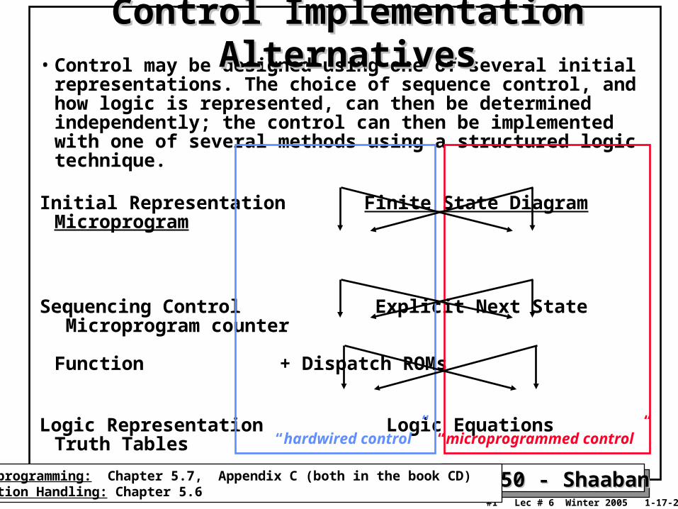
EECC550 - Shaaban EECC550 - Shaaban #1 Lec # 6 Winter 2005 1-17-2 • Control may be designed using one of several initial representations. The choice of sequence control, and how logic is represented, can then be determined independently; the control can then be implemented with one of several methods using a structured logic technique. Initial Representation Finite State Diagram Microprogram Sequencing Control Explicit Next State Microprogram counter Function + Dispatch ROMs Logic Representation Logic Equations Truth Tables “hardwired control” “microprogrammed control” Control Implementation Control Implementation Alternatives Alternatives programming: Chapter 5.7, Appendix C (both in the book CD) tion Handling: Chapter 5.6
-
date post
22-Dec-2015 -
Category
Documents
-
view
219 -
download
0
Transcript of EECC550 - Shaaban #1 Lec # 6 Winter 2005 1-17-2006 Control may be designed using one of several...
EECC550 - ShaabanEECC550 - Shaaban#1 Lec # 6 Winter 2005 1-17-2006
• Control may be designed using one of several initial representations. The choice of sequence control, and how logic is represented, can then be determined independently; the control can then be implemented with one of several methods using a structured logic technique.
Initial Representation Finite State Diagram Microprogram
Sequencing Control Explicit Next State Microprogram counter Function + Dispatch ROMs
Logic Representation Logic Equations Truth Tables
Implementation PLAROM Technique “hardwired control” “microprogrammed control”
Control Implementation AlternativesControl Implementation Alternatives
Microprogramming: Chapter 5.7, Appendix C (both in the book CD) Exception Handling: Chapter 5.6
EECC550 - ShaabanEECC550 - Shaaban#2 Lec # 6 Winter 2005 1-17-2006
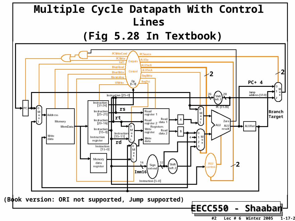
Multiple Cycle Datapath With Control Lines (Fig 5.28 In Textbook)
(Book version: ORI not supported, Jump supported)
PC+ 4
BranchTarget
rs
rt
rd
2
2
2
Imm16

EECC550 - ShaabanEECC550 - Shaaban#3 Lec # 6 Winter 2005 1-17-2006
The Effect of 1-bit Control Signals Signal Name
RegDst
RegWrite
ALUSrcA
MemRead
MemWrite
MemtoReg
IorD
IRWrite
PCWrite
PCWriteCond
Effect when deasserted (=0)
The register destination number for thewrite register comes from the rt field(instruction bits 20:16).
None
The first ALU operand is the PC
None
None
The value fed to the register write data input comes from ALUOut register.
The PC is used to supply the address to thememory unit.
None
None
None
Effect when asserted (=1)
The register destination number for thewrite register comes from the rd field(instruction bits 15:11).The register on the write register inputis written with the value on the Write data input.
The First ALU operand is register A (I.e R[rs])
Content of memory specified by the address input are put on the memory data output.
Memory contents specified by the address input is replaced by the value on the Write data input.
The value fed to the register write data input comes from data memory register (MDR).
The ALUOut register is used to supply the the address to the memory unit.
The output of the memory is written into Instruction Register (IR)
The PC is written; the source is controlled by PCSource
The PC is written if the Zero output of the ALU isalso active.
(Figure 5.29 page 324)
EECC550 - ShaabanEECC550 - Shaaban#4 Lec # 6 Winter 2005 1-17-2006
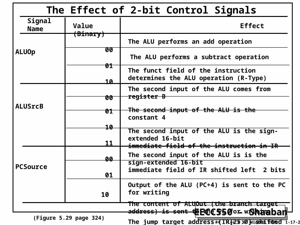
The Effect of 2-bit Control Signals Signal Name
ALUOp
ALUSrcB
PCSource
Value (Binary)
00
01
10
00
01
10
11
00
01
10
Effect
The ALU performs an add operation
The ALU performs a subtract operation
The funct field of the instruction determines the ALU operation (R-Type)
The second input of the ALU comes from register B
The second input of the ALU is the constant 4
The second input of the ALU is the sign-extended 16-bitimmediate field of the instruction in IR
The second input of the ALU is is the sign-extended 16-bitimmediate field of IR shifted left 2 bits
Output of the ALU (PC+4) is sent to the PC for writing
The content of ALUOut (the branch target address) is sent to the PC for writing
The jump target address (IR[25:0] shifted left 2 bits and concatenated with PC+4[31:28] is sent to the PC for writing
(Figure 5.29 page 324)

EECC550 - ShaabanEECC550 - Shaaban#5 Lec # 6 Winter 2005 1-17-2006
Instruction Fetch
Instruction Decode
Execution
Memory
WriteBack
R-Type
IR Mem[PC]PC PC + 4
A R[rs]
B R[rt]
ALUout PC + (SignExt(imm16) x4)
ALUout
A funct B
R[rd] ALUout
Load
IR Mem[PC]PC PC + 4
A R[rs]
B R[rt]
ALUout PC +
(SignExt(imm16) x4)
ALUout
A + SignEx(Im16)
M Mem[ALUout]
R[rt] M
Store
IR Mem[PC]PC PC + 4
A R[rs]
B R[rt]
ALUout PC +
(SignExt(imm16) x4)
ALUout
A + SignEx(Im16)
Mem[ALUout] B
Branch
IR Mem[PC]PC PC + 4
A R[rs]
B R[rt]
ALUout PC +
(SignExt(imm16) x4)
Zero A - B
Zero: PC ALUout
IF
ID
EX
MEM
WB
Jump
IR Mem[PC]PC PC + 4
A R[rs]
B R[rt]
ALUout PC +
(SignExt(imm16) x4)
PC Jump Address
Instruction Fetch (IF) & Instruction Decode cycles are common for all instructions
Operations (Dependant RTN) for Each CycleOperations (Dependant RTN) for Each Cycle
EECC550 - ShaabanEECC550 - Shaaban#6 Lec # 6 Winter 2005 1-17-2006
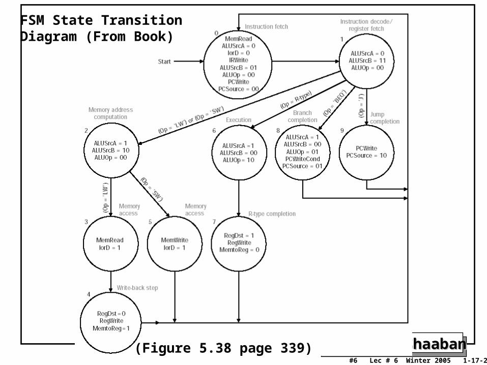
FSM State TransitionDiagram (From Book)
(Figure 5.38 page 339)
EECC550 - ShaabanEECC550 - Shaaban#7 Lec # 6 Winter 2005 1-17-2006
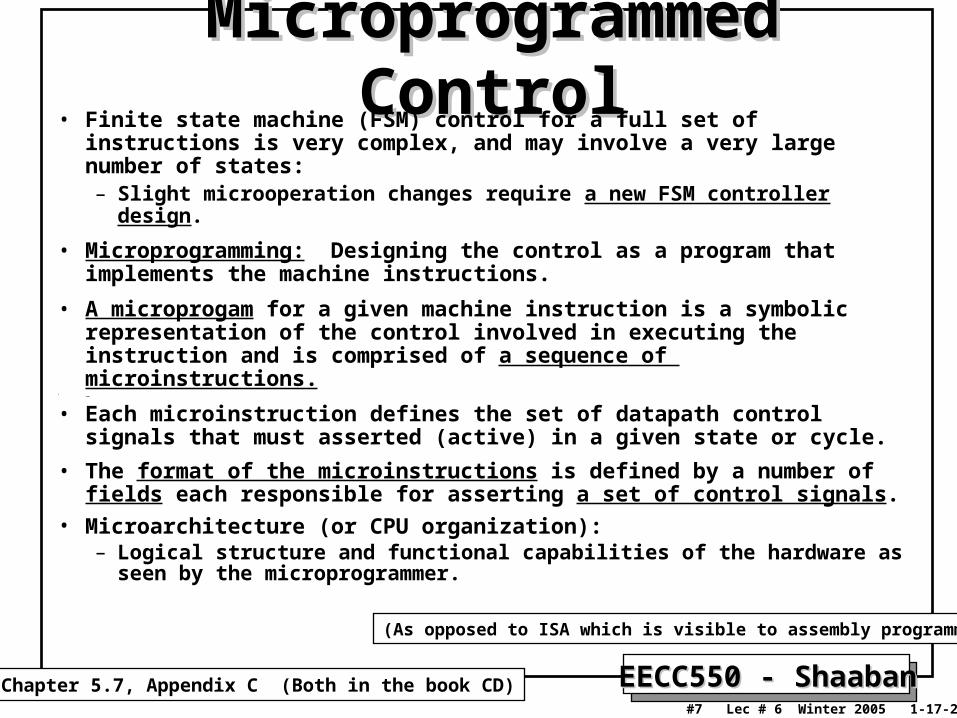
Microprogrammed ControlMicroprogrammed Control• Finite state machine (FSM) control for a full set of instructions is very
complex, and may involve a very large number of states:– Slight microoperation changes require a new FSM controller design.
• Microprogramming: Designing the control as a program that implements the machine instructions.
• A microprogam for a given machine instruction is a symbolic representation of the control involved in executing the instruction and is comprised of a sequence of microinstructions.
•
• Each microinstruction defines the set of datapath control signals that must asserted (active) in a given state or cycle.
• The format of the microinstructions is defined by a number of fields each responsible for asserting a set of control signals.
• Microarchitecture (or CPU organization):– Logical structure and functional capabilities of the hardware as seen
by the microprogrammer.
Chapter 5.7, Appendix C (Both in the book CD)
(As opposed to ISA which is visible to assembly programmer)
EECC550 - ShaabanEECC550 - Shaaban#8 Lec # 6 Winter 2005 1-17-2006
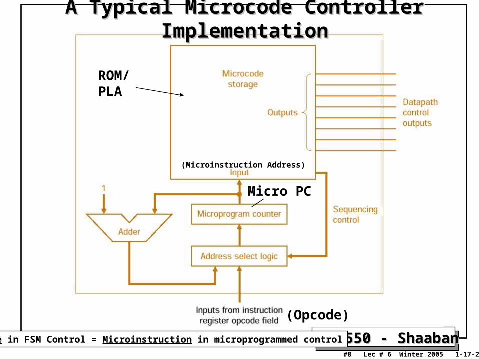
A Typical Microcode Controller ImplementationA Typical Microcode Controller Implementation
ROM/PLA
Micro PC
(Opcode)
(Microinstruction Address)
State in FSM Control = Microinstruction in microprogrammed control
EECC550 - ShaabanEECC550 - Shaaban#9 Lec # 6 Winter 2005 1-17-2006
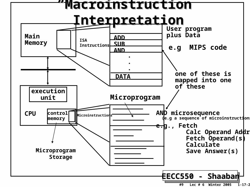
““Macroinstruction” InterpretationMacroinstruction” Interpretation
MainMemory
executionunit
controlmemory
CPU
ADDSUBAND
DATA
.
.
.
User program plus Data
AND microsequence
e.g., Fetch Calc Operand Addr Fetch Operand(s) Calculate Save Answer(s)
one of these ismapped into oneof these
Microprogram Storage
e.g MIPS code
Microprogram
ISAInstructions
Microinstructions(e.g a sequence of microinstructions)

EECC550 - ShaabanEECC550 - Shaaban#10 Lec # 6 Winter 2005 1-17-2006
Design of Microinstruction Design of Microinstruction Format/AddressingFormat/Addressing
• Start with a list of all control signals needed.
• Partition control signals with similar functions into a number of signal sets that share a single microinstruction field.
• A sequencing microinstruction field is used to indicate the next microinstruction to execute.
• Place fields in some logical order (e.g., ALU operation & ALU operands first and microinstruction sequencing last).
• Since microinstructions are placed in a ROM or PLA, addresses must be assigned to microinstructions, usually sequentially.
• Create a symbolic legend for the microinstruction format, showing name of field values and how they set the control signals.
• To minimize microinstruction width, operations that will never be used at the same time may be encoded.
EECC550 - ShaabanEECC550 - Shaaban#11 Lec # 6 Winter 2005 1-17-2006
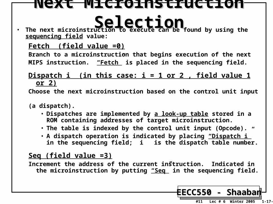
Next Microinstruction SelectionNext Microinstruction Selection• The next microinstruction to execute can be found by using the sequencing field
value:
Fetch (field value =0)Branch to a microinstruction that begins execution of the next MIPS instruction. “Fetch” is placed in the sequencing field.
Dispatch i (in this case: i = 1 or 2 , field value 1 or 2)Choose the next microinstruction based on the control unit input (a dispatch).
• Dispatches are implemented by a look-up table stored in a ROM containing addresses of target microinstruction.
• The table is indexed by the control unit input (Opcode).• A dispatch operation is indicated by placing “Dispatch i” in the
sequencing field; i is the dispatch table number.
Seq (field value =3)Increment the address of the current instruction. Indicated in the
microinstruction by putting “Seq” in the sequencing field.
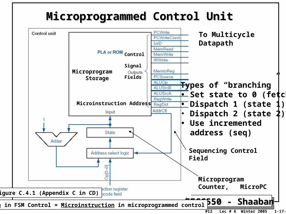
EECC550 - ShaabanEECC550 - Shaaban#12 Lec # 6 Winter 2005 1-17-2006
Types of “branching”• Set state to 0 (fetch)• Dispatch 1 (state 1)• Dispatch 2 (state 2)• Use incremented address (seq)
Microinstruction Address
Control Signal Fields
Microprogram Storage
To MulticycleDatapath
MicroprogramCounter, MicroPC
Sequencing Control Field
Microprogrammed Control UnitMicroprogrammed Control Unit
Figure C.4.1 (Appendix C in CD)
State in FSM Control = Microinstruction in microprogrammed control
EECC550 - ShaabanEECC550 - Shaaban#13 Lec # 6 Winter 2005 1-17-2006
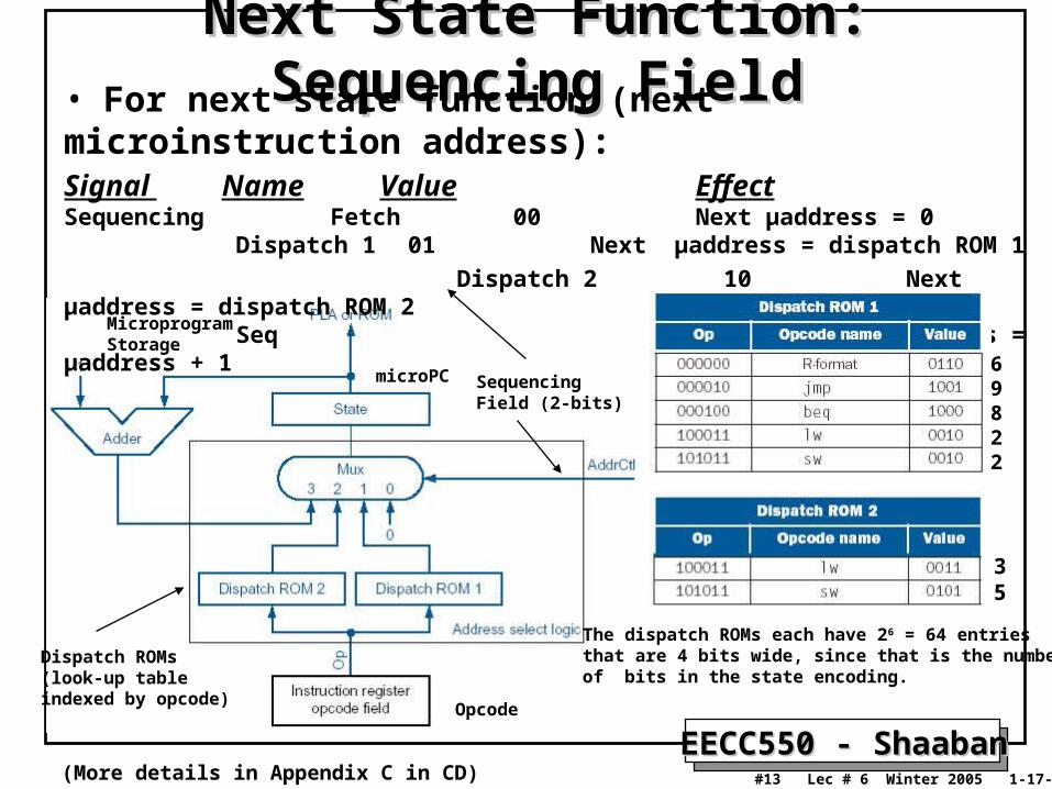
Next State Function: Sequencing FieldNext State Function: Sequencing Field• For next state function (next microinstruction address):Signal Name Value Effect Sequencing Fetch 00 Next µaddress = 0 Dispatch 1 01 Next µaddress = dispatch ROM 1
Dispatch 2 10 Next µaddress = dispatch ROM 2 Seq 11 Next µaddress = µaddress + 1
microPC
Microprogram Storage
Dispatch ROMs(look-up table indexed by opcode)
Opcode
SequencingField (2-bits)
The dispatch ROMs each have 26 = 64 entries that are 4 bits wide, since that is the number of bits in the state encoding.
(More details in Appendix C in CD)
69822
35
EECC550 - ShaabanEECC550 - Shaaban#14 Lec # 6 Winter 2005 1-17-2006
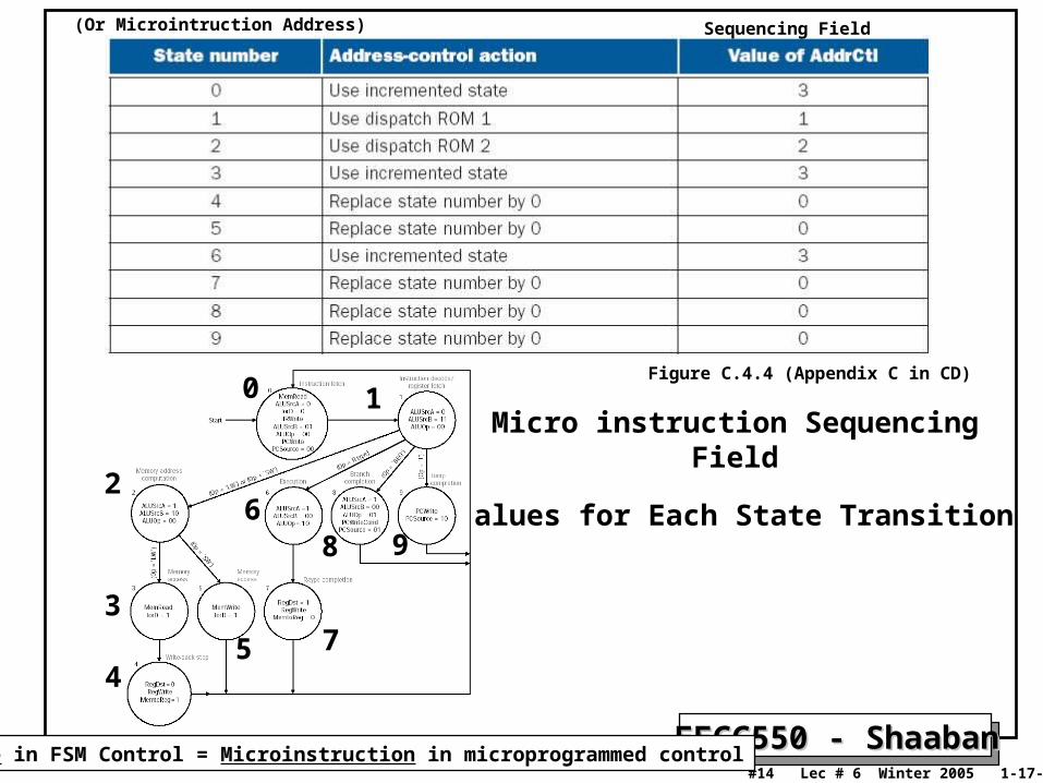
Micro instruction Sequencing Field
Values for Each State Transition
0 1
Sequencing Field
26
8 9
3
5 74
(Or Microintruction Address)
State in FSM Control = Microinstruction in microprogrammed control
Figure C.4.4 (Appendix C in CD)

EECC550 - ShaabanEECC550 - Shaaban#15 Lec # 6 Winter 2005 1-17-2006
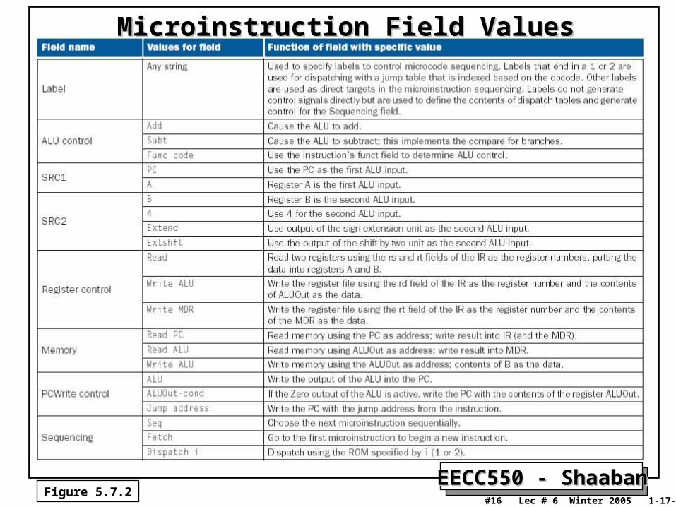
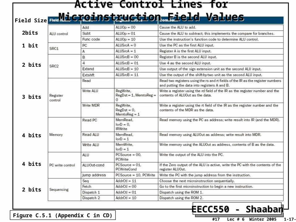
Microinstruction FormatMicroinstruction Format
Field Name Field Width (bits) Control Signals Set in Field
ALU Control 2 ALUOp
SRC1 1 ALUSrcA
SRC2 2 ALUSrcB
Register Control 3 RegWrite, MemtoReg, RegDst
Memory 4 MemRead, MemWrite, IorD, IRWrite
PCWrite Control 4 PCWrite, PCWriteCond, PCSource
Sequencing 2 AddrCtl
Total width 18 bits
ALU Control
SRC1 SRC2Register Control
MemoryPCWrite Control
Sequencing
2 bits 1 bit 2 bits 3 bits 4 bits 4 bits 2 bits
EECC550 - ShaabanEECC550 - Shaaban#16 Lec # 6 Winter 2005 1-17-2006
Microinstruction Field ValuesMicroinstruction Field Values
Figure 5.7.2
EECC550 - ShaabanEECC550 - Shaaban#17 Lec # 6 Winter 2005 1-17-2006
Figure C.5.1 (Appendix C in CD)
Active Control Lines for Microinstruction Field ValuesActive Control Lines for Microinstruction Field Values
2bits
1 bit
2 bits
3 bits
4 bits
4 bits
2 bits
Field Size
EECC550 - ShaabanEECC550 - Shaaban#18 Lec # 6 Winter 2005 1-17-2006
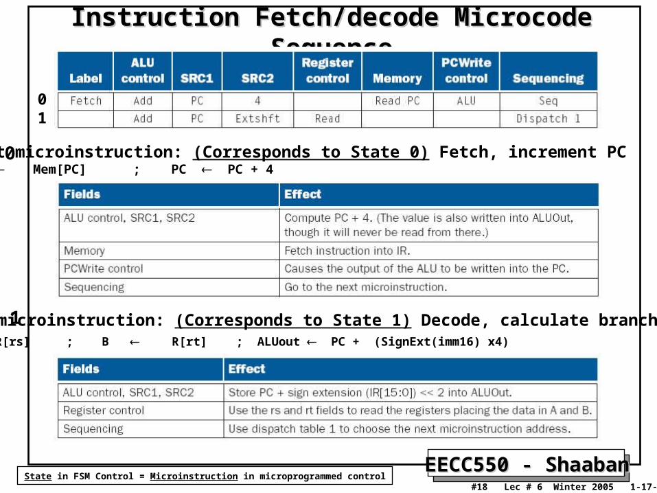
Instruction Fetch/decode Microcode SequenceInstruction Fetch/decode Microcode Sequence
First microinstruction: (Corresponds to State 0) Fetch, increment PCIR Mem[PC] ; PC PC + 4
Second microinstruction: (Corresponds to State 1) Decode, calculate branch addressA R[rs] ; B R[rt] ; ALUout PC + (SignExt(imm16) x4)
01
0
1
State in FSM Control = Microinstruction in microprogrammed control
EECC550 - ShaabanEECC550 - Shaaban#19 Lec # 6 Winter 2005 1-17-2006
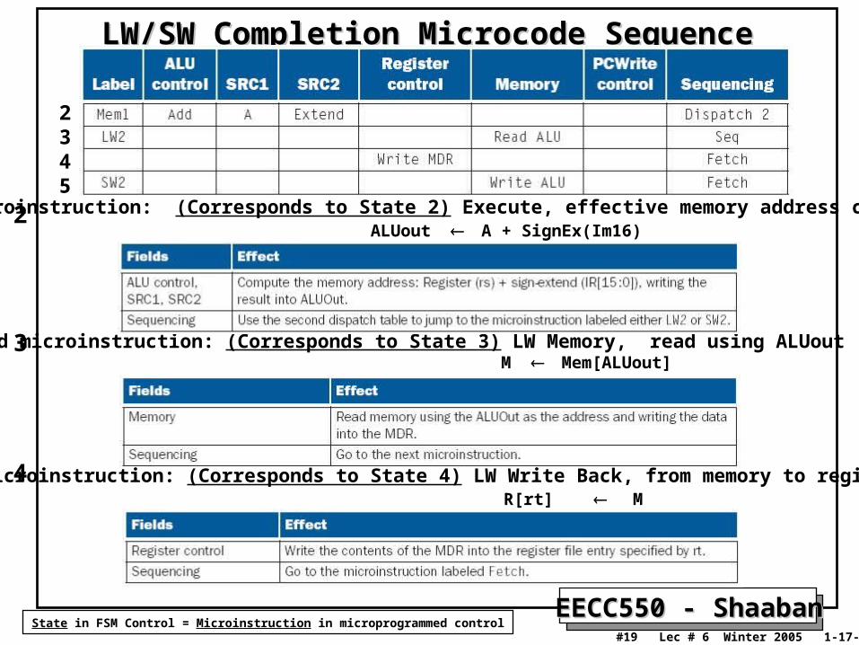
LW/SW Completion Microcode SequenceLW/SW Completion Microcode Sequence
First microinstruction: (Corresponds to State 2) Execute, effective memory address calculation ALUout A + SignEx(Im16)
Second microinstruction: (Corresponds to State 3) LW Memory, read using ALUout M Mem[ALUout]
Third microinstruction: (Corresponds to State 4) LW Write Back, from memory to register rt R[rt] M
2345
2
3
4
State in FSM Control = Microinstruction in microprogrammed control
EECC550 - ShaabanEECC550 - Shaaban#20 Lec # 6 Winter 2005 1-17-2006
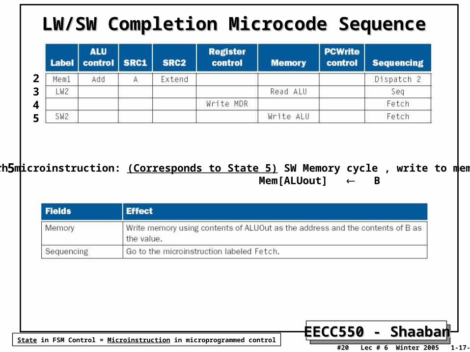
Fourh microinstruction: (Corresponds to State 5) SW Memory cycle , write to memory Mem[ALUout] B
LW/SW Completion Microcode SequenceLW/SW Completion Microcode Sequence
2345
5
State in FSM Control = Microinstruction in microprogrammed control

EECC550 - ShaabanEECC550 - Shaaban#21 Lec # 6 Winter 2005 1-17-2006
R-Type Completion Microcode SequenceR-Type Completion Microcode Sequence
First microinstruction: (Corresponds to State 6) Execute, perform ALU function
ALUout A funct B
Second microinstruction: (Corresponds to State 7) Write Back, ALU result in register rd R[rd] ALUout
67
6
7
State in FSM Control = Microinstruction in microprogrammed control
EECC550 - ShaabanEECC550 - Shaaban#22 Lec # 6 Winter 2005 1-17-2006
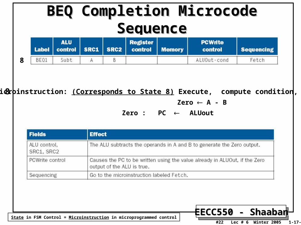
BEQ Completion Microcode SequenceBEQ Completion Microcode Sequence
First microinstruction: (Corresponds to State 8) Execute, compute condition, update PC
Zero A - B
Zero : PC ALUout
8
8
State in FSM Control = Microinstruction in microprogrammed control

EECC550 - ShaabanEECC550 - Shaaban#23 Lec # 6 Winter 2005 1-17-2006
Jump Completion Microcode SequenceJump Completion Microcode Sequence
First microinstruction: (Corresponds to State 9) Execute, update PC with Jump Address
PC Jump Address
9
9
State in FSM Control = Microinstruction in microprogrammed control
EECC550 - ShaabanEECC550 - Shaaban#24 Lec # 6 Winter 2005 1-17-2006
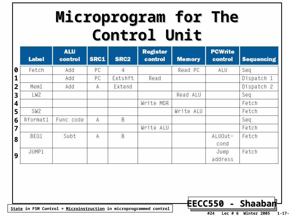
Microprogram for The Control UnitMicroprogram for The Control Unit
01234567
8
9
State in FSM Control = Microinstruction in microprogrammed control
EECC550 - ShaabanEECC550 - Shaaban#25 Lec # 6 Winter 2005 1-17-2006
Microprogramming Pros and ConsMicroprogramming Pros and ConsPros:• Ease of design.
• Flexibility:– Easy to adapt to changes in organization, timing, technology.– Can make changes late in design cycle, or even in the field.
• Can implement very powerful instruction sets (just more microprogram control memory is needed).
• Generality:– Can implement multiple instruction sets on the same machine.– Can tailor instruction set to application.
• Compatibility:– Many organizations, same instruction set.
Cons:• Possibly more costly to implement than FSM control.
• Usually slower than FSM control.
EECC550 - ShaabanEECC550 - Shaaban#26 Lec # 6 Winter 2005 1-17-2006
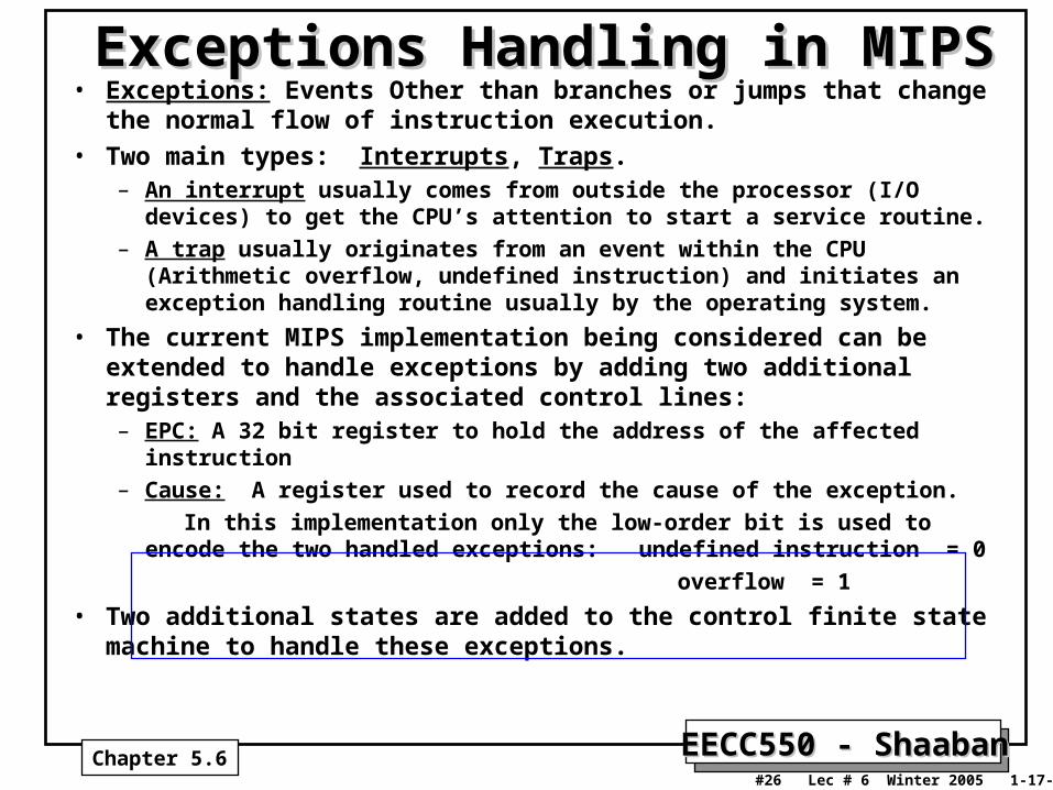
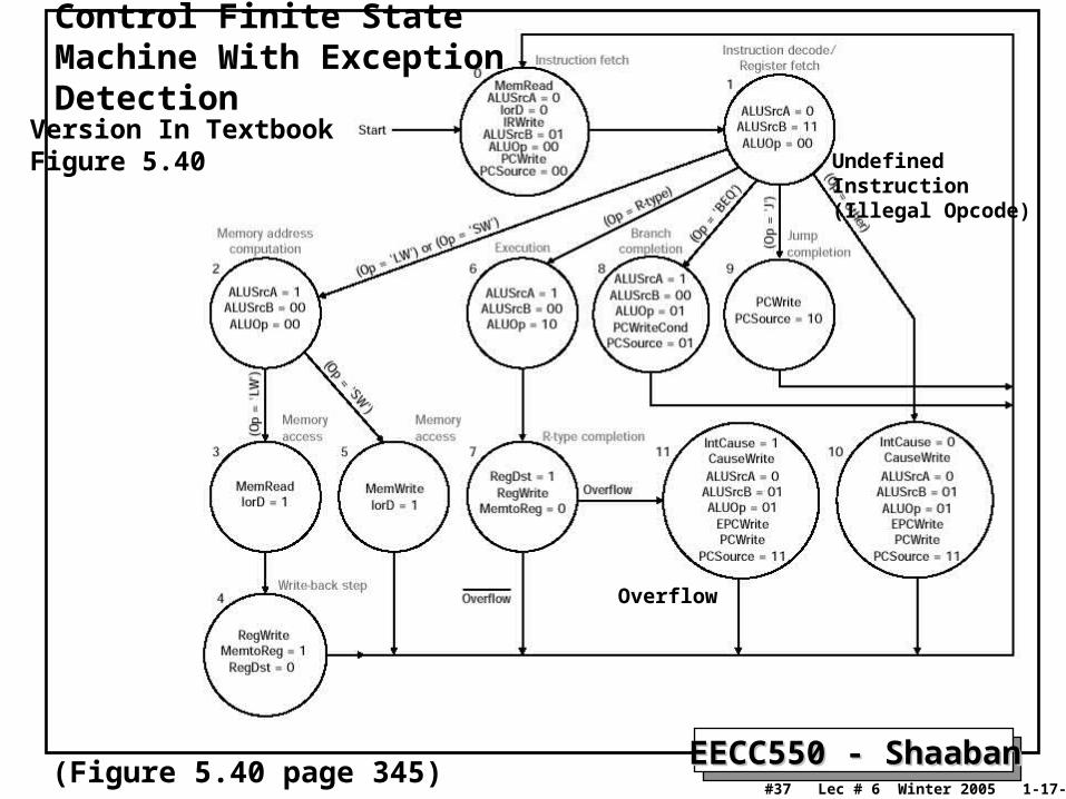
Exceptions Handling in MIPSExceptions Handling in MIPS• Exceptions: Events Other than branches or jumps that change the
normal flow of instruction execution.• Two main types: Interrupts, Traps.
– An interrupt usually comes from outside the processor (I/O devices) to get the CPU’s attention to start a service routine.
– A trap usually originates from an event within the CPU (Arithmetic overflow, undefined instruction) and initiates an exception handling routine usually by the operating system.
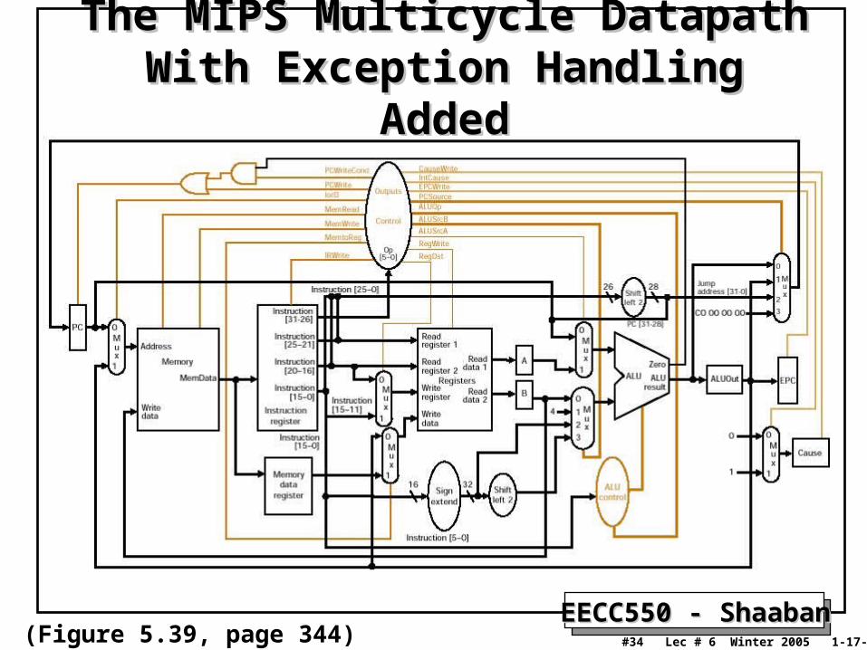
• The current MIPS implementation being considered can be extended to handle exceptions by adding two additional registers and the associated control lines:
– EPC: A 32 bit register to hold the address of the affected instruction– Cause: A register used to record the cause of the exception.
In this implementation only the low-order bit is used to encode the two handled exceptions: undefined instruction = 0
overflow = 1
• Two additional states are added to the control finite state machine to handle these exceptions.
Chapter 5.6

EECC550 - ShaabanEECC550 - Shaaban#27 Lec # 6 Winter 2005 1-17-2006
Two Types of ExceptionsTwo Types of Exceptions• Interrupts:
– Caused by external events (e.g. I/O device requests).
– Asynchronous to program execution.
– May be handled between instructions.
– Simply suspend and resume user program.
• Traps:– Caused by internal events:
• Exceptional conditions (e.g. overflow).• Errors (e.g memory parity error).• Faults (e.g. Page fault, non-resident page).
– Synchronous to program execution.
– Condition must be remedied by the system exception handler.
– Instruction may be executed again and program continued or program may be aborted.

EECC550 - ShaabanEECC550 - Shaaban#28 Lec # 6 Winter 2005 1-17-2006
Exception HandlingException Handling
• Exception = an unprogrammed control transfer– System takes action to handle the exception which include:
• Recording the address of the offending instruction.
• Saving & restoring user program state.
• Returning control to user (unless user program is aborted).
user programSystemExceptionHandlerException:
return fromexception
1 Save State 2 OSExceptionHandling
3Returnto user program
EECC550 - ShaabanEECC550 - Shaaban#29 Lec # 6 Winter 2005 1-17-2006
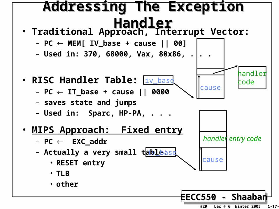
Addressing The Exception HandlerAddressing The Exception Handler• Traditional Approach, Interrupt Vector:
– PC MEM[ IV_base + cause || 00]– Used in: 370, 68000, Vax, 80x86, . . .
• RISC Handler Table:– PC IT_base + cause || 0000– saves state and jumps– Used in: Sparc, HP-PA, . . .
• MIPS Approach: Fixed entry– PC EXC_addr– Actually a very small table:
• RESET entry• TLB • other
iv_basecause
handlercode
iv_basecause
handler entry code

EECC550 - ShaabanEECC550 - Shaaban#30 Lec # 6 Winter 2005 1-17-2006
Exception Handling: Exception Handling: Saving The StateSaving The State
• Push it onto the stack:– Vax, 68k, x86
• Save it in special registers:– MIPS: EPC, BadVaddr, Status, Cause
• Shadow Registers:– M88k.
• Save state in a shadow (a copy) of the internal CPU registers.
EECC550 - ShaabanEECC550 - Shaaban#31 Lec # 6 Winter 2005 1-17-2006
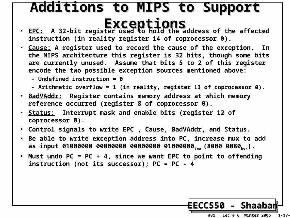
Additions to MIPS to Support ExceptionsAdditions to MIPS to Support Exceptions• EPC: A 32-bit register used to hold the address of the affected instruction
(in reality register 14 of coprocessor 0).
• Cause: A register used to record the cause of the exception. In the MIPS architecture this register is 32 bits, though some bits are currently unused. Assume that bits 5 to 2 of this register encode the two possible exception sources mentioned above: – Undefined instruction = 0
– Arithmetic overflow = 1 (in reality, register 13 of coprocessor 0).
• BadVAddr: Register contains memory address at which memory reference occurred (register 8 of coprocessor 0).
• Status: Interrupt mask and enable bits (register 12 of coprocessor 0).
• Control signals to write EPC , Cause, BadVAddr, and Status.
• Be able to write exception address into PC, increase mux to add as input 01000000 00000000 00000000 01000000two (8000 0080hex).
• Must undo PC = PC + 4, since we want EPC to point to offending instruction (not its successor); PC = PC - 4
EECC550 - ShaabanEECC550 - Shaaban#32 Lec # 6 Winter 2005 1-17-2006
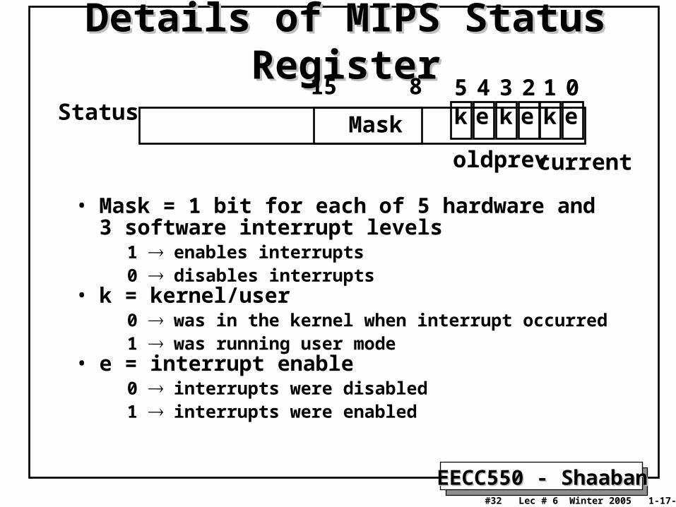
Details of MIPS Status RegisterDetails of MIPS Status Register
• Mask = 1 bit for each of 5 hardware and 3 software interrupt levels
1 enables interrupts0 disables interrupts
• k = kernel/user0 was in the kernel when interrupt occurred1 was running user mode
• e = interrupt enable0 interrupts were disabled1 interrupts were enabled
Status15 8 5
k4e
3k
2e
1k
0eMask
old prev current
EECC550 - ShaabanEECC550 - Shaaban#33 Lec # 6 Winter 2005 1-17-2006
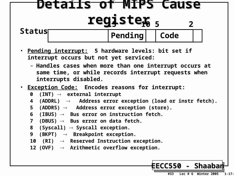
Details of MIPS Cause registerDetails of MIPS Cause register
• Pending interrupt: 5 hardware levels: bit set if interrupt occurs but not yet serviced:– Handles cases when more than one interrupt occurs at same time,
or while records interrupt requests when interrupts disabled.• Exception Code: Encodes reasons for interrupt:
0 (INT) external interrupt4 (ADDRL) Address error exception (load or instr fetch).5 (ADDRS) Address error exception (store).6 (IBUS) Bus error on instruction fetch.7 (DBUS) Bus error on data fetch.8 (Syscall) Syscall exception.9 (BKPT) Breakpoint exception.10 (RI) Reserved Instruction exception.12 (OVF) Arithmetic overflow exception.
Status15 10
Pending
5 2
Code
EECC550 - ShaabanEECC550 - Shaaban#34 Lec # 6 Winter 2005 1-17-2006
The MIPS Multicycle Datapath With The MIPS Multicycle Datapath With Exception Handling AddedException Handling Added
(Figure 5.39, page 344)

EECC550 - ShaabanEECC550 - Shaaban#35 Lec # 6 Winter 2005 1-17-2006
Finite State Machine (FSM) SpecificationFinite State Machine (FSM) SpecificationIR MEM[PC]
PC PC + 4
R-type
ALUout A fun B
R[rd] ALUout
ALUout A op ZX
R[rt] ALUout
ORiALUout
A + SX
R[rt] M
M MEM[ALUout]
LW
ALUout A + SX
MEM[ALUout] B
SW
“instruction fetch”
“decode”
Exe
cute
Mem
ory
Writ
e-ba
ck
0000
0001
0100
0101
0110
0111
1000
1001
1010
1011
1100
BEQ
0010
If A = B then PC ALUout
A R[rs]B R[rt]
ALUout PC +SX
To instruction fetch
To instruction fetchTo instruction fetch
EECC550 - ShaabanEECC550 - Shaaban#36 Lec # 6 Winter 2005 1-17-2006
FSM Control Specification To Handle ExceptionsFSM Control Specification To Handle ExceptionsIR MEM[PC]
PC PC + 4
R-type
ALUout A fun B
R[rd] ALUout
ALUout A op ZX
R[rt] ALUout
ORiALUout
A + SX
R[rt] M
M MEM[ALUout]
LW
ALUout A + SX
MEM[ALUout] B
SW
“instruction fetch”
“decode”
Exe
cute
Mem
ory
Writ
e-ba
ck
0000
0001
0100
0101
0110
0111
1000
1001
1010
1011
1100
A R[rs]B R[rt]
ALUout PC +SX EPC PC - 4
PC exp_addrcause 0
undefined instruction
EPC PC - 4PC exp_addrcause 1
overflow
BEQ
0010
If A = B then PC ALUout
To instruction fetch
To instruction fetchTo instruction fetch
EECC550 - ShaabanEECC550 - Shaaban#37 Lec # 6 Winter 2005 1-17-2006
Control Finite State Machine With Exception Detection
Version In TextbookFigure 5.40 Undefined
Instruction(Illegal Opcode)
Overflow
(Figure 5.40 page 345)