EE Technologies, Inc. – Electronics Manufacturing in Mexico (EMS)
1
EE 2109 Electronics-I
Dr. Mostafa Zaman Chowdhury
Dept. of Electrical and Electronic Engineering, KUET
Presentation #1

EE 2109 Electronics-I
Credit: 3, Contact Hours: 3 Hrs/Week
Syllabus Introduction: Properties of Insulators, Semiconductors, and Metals; Conduction in
solids, Conventional current and electron flow, Drift and diffusion current, Mobility and Conductivity. The potential barrier; work function; contact potential. The Hall Effect and Hall devices.
Semiconductors: Intrinsic Semiconductors: Crystal and energy band diagram, Electrons and holes, conduction in semiconductors, Electron and hole concentration. Extrinsic semiconductors: n-type doping, p-type doping, and compensation doping, Temperature dependence of conductivity, Carrier Concentration Temperature Dependence, Degenerate and non-degenerate semiconductors. Diffusion and conduction equations, random motion and continuity equation, Time-dependent continuity equation, Steady-state continuity equation.
Semiconductor diode characteristics: Qualitative and Quantitative theory of the p-n junction as a diode; Ideal pn junction, pn junction band diagram, current components in p-n diode; Volt-ampere characteristics; Transition and diffusion capacitance, Dynamic resistance, Reverse breakdown; Avalanche and Zener breakdown; Zenerdiode, Rectifier Diode: controlled & uncontrolled rectification, Special-Purpose Diodes: Tunnel diode, varactor diode, and breakdown diode; Metal oxide semi-conductor diode, optical diode, PIN diode, Schottky diode, Current regulator diode.
Transistor: Transistor and its current components, transistor as an amplifier, BJT, Different transistor configurations, study of load lines, transistor switching times, detailed study of transistor biasing and thermal stabilization.
Dept. of Electrical and Electronic Engineering, KUET 2

References
Electronic Devices and Circuit Theory by Robert L.
Boylestad
Principle of Electronic Materials and Devices by S O
Kasap
Electronic Devices and Circuits by Jacob Millman
Principle of Electronics by V. K. Mehta
3Dept. of Electrical and Electronic Engineering, KUET

Semiconductor Materials
Dept. of Electrical and Electronic Engineering, KUET 4
Materials commonly used in the development of semiconductor devices Silicon (Si)
Germanium (Ge)
Gallium Arsenide (GaAs)

Doping
The electrical characteristics of silicon and germanium are improved by adding materials in a process called doping.
There are just two types of doped semiconductor materials n-type
p-type
n-type materials contain an excess of conduction band electrons.
p-type materials contain an excess of valence band holes.
Dept. of Electrical and Electronic Engineering, KUET 5

Dept. of Electrical and Electronic Engineering, KUET 6
Majority and Minority Carriers
Two currents through a diode
Majority Carriers
− The majority carriers in n-type materials are electrons.
− The majority carriers in p-type materials are holes.
Minority Carriers
− The minority carriers in n-type materials are holes.
− The minority carriers in p-type materials are electrons.

p-n Junctions (1/2)
One end of a silicon or germanium crystal can be doped as a
p-type material and the other end as an n-type material.
The result is a p-n junction
Dept. of Electrical and Electronic Engineering, KUET 7

Dept. of Electrical and Electronic Engineering, KUET 8
p-n Junctions (2/2)
At the p-n junction, the excess conduction-band electrons on the n-type side are attracted to the valence-band holes on the p-type side.
The electrons in the n-type material migrate across the junction to the p-type material (electron flow).
The electron migration results in a negative charge on the p-type side of the junction and a positive charge on the n-type side of the junction.
The result is the formation of a
depletion region around the
junction.
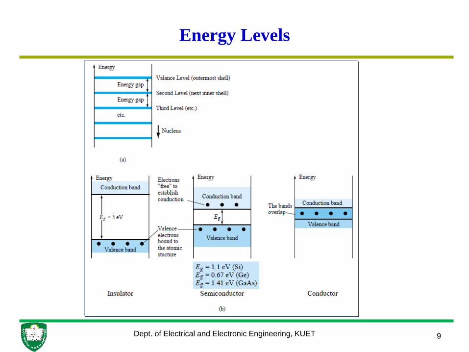
Energy Levels
Dept. of Electrical and Electronic Engineering, KUET 9

Extrinsic Materials (1/2)
A semiconductor material that
has been subjected to the doping
process is called an extrinsic
material
n-Type Material
The n-type is created by
introducing those impurity
elements that have five valence
electrons (pentavalent), such as
antimony, arsenic, and
phosphorus.
10Dept. of Electrical and Electronic Engineering, KUET

Extrinsic Materials (2/2)
p-Type Material
The p-type material is formed
by doping a pure germanium
or silicon crystal with impurity
atoms having three valence
electrons
11Dept. of Electrical and Electronic Engineering, KUET
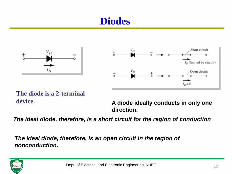
Diodes
Dept. of Electrical and Electronic Engineering, KUET 12
The diode is a 2-terminal
device. A diode ideally conducts in only one
direction.
The ideal diode, therefore, is a short circuit for the region of conduction
The ideal diode, therefore, is an open circuit in the region of
nonconduction.

Diode Characteristics
Conduction Region
The voltage across the diode is 0 V
The current is infinite
The forward resistance is defined
as RF = VF / IF
The diode acts like a short
Dept. of Electrical and Electronic Engineering, KUET 13
Non-conduction Region
All of the voltage is across the
diode
The current is 0 A
The reverse resistance is
defined as RR = VR / IR
The diode acts like open

Diode Operating Conditions
A diode has three operating conditions
No bias
Forward bias
Reverse bias
Dept. of Electrical and Electronic Engineering, KUET 14
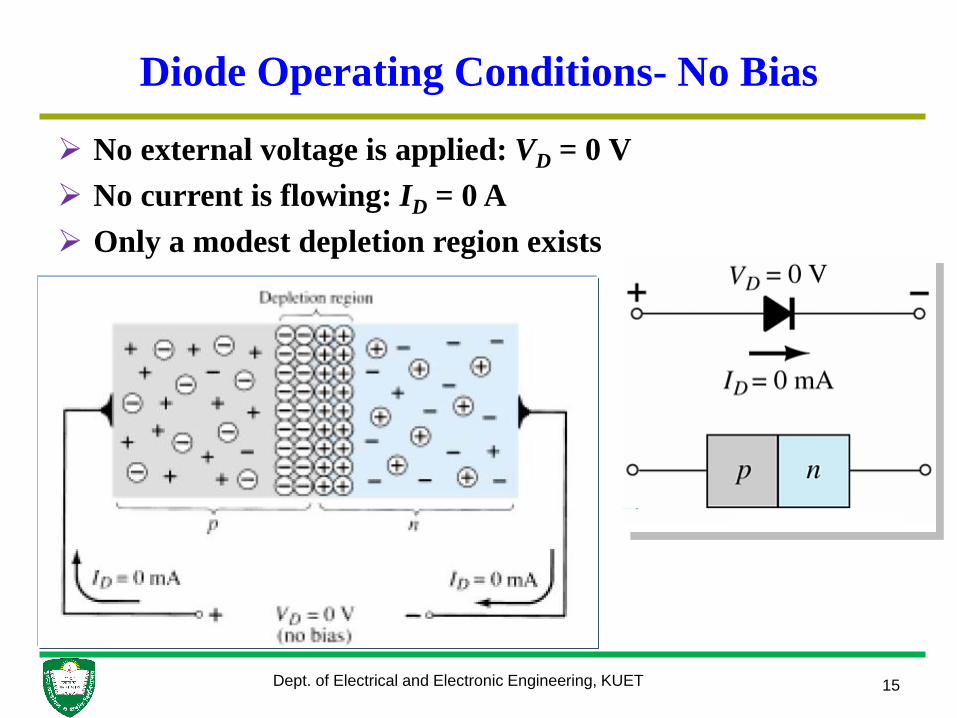
Diode Operating Conditions- No Bias
No external voltage is applied: VD = 0 V
No current is flowing: ID = 0 A
Only a modest depletion region exists
Dept. of Electrical and Electronic Engineering, KUET 15

Diode Operating Conditions- Reverse Bias
External voltage is applied across the p-n junction in the opposite
polarity of the p- and n-type materials.
The reverse voltage causes the depletion region to widen.
The electrons in the n-type material are attracted toward the positive
terminal of the voltage source.
The holes in the p-type material are attracted toward the negative
terminal of the voltage source.
Dept. of Electrical and Electronic Engineering, KUET 16

Diode Operating Conditions- Forward Bias
External voltage is applied across the p-n junction in the
same polarity as the p- and n-type materials.
The forward voltage causes the depletion region to narrow
The electrons and holes are pushed toward the p-n junction
The electrons and holes have sufficient energy to cross the p-
n junction.
Dept. of Electrical and Electronic Engineering, KUET 17

Actual Diode Characteristics
Note the regions for
no bias, reverse
bias, and forward
bias conditions.
Carefully note the
scale for each of
these conditions.
Dept. of Electrical and Electronic Engineering, KUET 18

Zener Region
The Zener region is in the diode’s
reverse-bias region.
At some point the reverse bias voltage is
so large the diode breaks down and the
reverse current increases dramatically
The maximum reverse-bias potential
that can be applied before entering the
Zener region is called the peak inverse
voltage (referred to simply as the PIV
rating) or the peak reverse voltage
(denoted by PRV rating).
The voltage that causes a diode to enter
the zener region of operation is called
the zener voltage (VZ).
Dept. of Electrical and Electronic Engineering, KUET 19

Forward Bias Voltage
The point at which the diode changes from no-bias
condition to forward-bias condition occurs when the
electrons and holes are given sufficient energy to cross the
p-n junction. This energy comes from the external voltage
applied across the diode.
The forward bias voltage required for a
gallium arsenide diode 1.2 V
silicon diode 0.7 V
germanium diode 0.3 V
Dept. of Electrical and Electronic Engineering, KUET 20

Temperature Effects
As temperature increases it adds energy to the
diode.
It reduces the required forward bias voltage for
forward-bias conduction.
It increases the amount of reverse current in the
reverse-bias condition.
It increases maximum reverse bias avalanche voltage.
Germanium diodes are more sensitive to temperature
variations than silicon or gallium arsenide diodes.
Dept. of Electrical and Electronic Engineering, KUET 21

Resistance Levels
Semiconductors react differently to DC and AC
currents.
There are three types of resistance DC (static) resistance
AC (dynamic) resistance
Average AC resistance
Dept. of Electrical and Electronic Engineering, KUET 22

AC (Dynamic) Resistance
In the forward bias region
• The resistance depends on the amount of current (ID) in the diode.
• The voltage across the diode is fairly constant (26 mV for 25C).
• rB ranges from a typical 0.1 for high power devices to 2 for low power, general purpose
diodes. In some cases rB can be ignored.
In the reverse bias region
Dept. of Electrical and Electronic Engineering, KUET 23
B
D
d rI
r mV 26
rd

Average AC Resistance
AC resistance can be calculated using the current and voltage values for
two points on the diode characteristic curve.
Dept. of Electrical and Electronic Engineering, KUET 24
pt. to pt. d
dav
ΔI
ΔV r

Diode Equivalent Circuit
Dept. of Electrical and Electronic Engineering, KUET 25

Diode Capacitance
In reverse bias, the depletion layer is very large. The diode’s strong positive
and negative polarities create capacitance, CT. The amount of capacitance
depends on the reverse voltage applied.
This is transition or depletion region capacitance
In forward bias storage capacitance or diffusion capacitance (CD) exists as the
diode voltage increases.
Dept. of Electrical and Electronic Engineering, KUET 26

Reverse Recovery Time (trr)
Reverse recovery time is the time required for a diode to stop
conducting once it is switched from forward bias to reverse bias.
Dept. of Electrical and Electronic Engineering, KUET 27
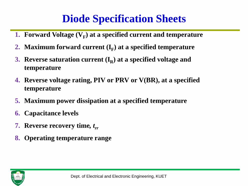
Diode Specification Sheets
1. Forward Voltage (VF) at a specified current and temperature
2. Maximum forward current (IF) at a specified temperature
3. Reverse saturation current (IR) at a specified voltage and
temperature
4. Reverse voltage rating, PIV or PRV or V(BR), at a specified
temperature
5. Maximum power dissipation at a specified temperature
6. Capacitance levels
7. Reverse recovery time, trr
8. Operating temperature range
Dept. of Electrical and Electronic Engineering, KUET

Zener Diode
A Zener is a diode operated in reverse bias at the Zener
voltage (VZ).
Common Zener voltages are between 1.8 V and 200 V
Wireless Networks & Communications Lab. 29
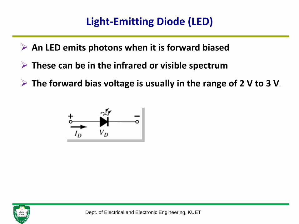
Light-Emitting Diode (LED)
An LED emits photons when it is forward biased
These can be in the infrared or visible spectrum
The forward bias voltage is usually in the range of 2 V to 3 V.
Dept. of Electrical and Electronic Engineering, KUET
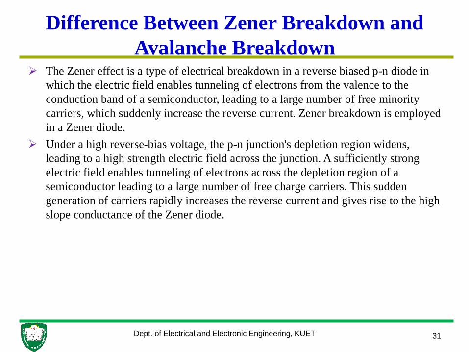
Difference Between Zener Breakdown and
Avalanche Breakdown The Zener effect is a type of electrical breakdown in a reverse biased p-n diode in
which the electric field enables tunneling of electrons from the valence to the
conduction band of a semiconductor, leading to a large number of free minority
carriers, which suddenly increase the reverse current. Zener breakdown is employed
in a Zener diode.
Under a high reverse-bias voltage, the p-n junction's depletion region widens,
leading to a high strength electric field across the junction. A sufficiently strong
electric field enables tunneling of electrons across the depletion region of a
semiconductor leading to a large number of free charge carriers. This sudden
generation of carriers rapidly increases the reverse current and gives rise to the high
slope conductance of the Zener diode.
31Dept. of Electrical and Electronic Engineering, KUET

Difference Between Zener Breakdown and
Avalanche Breakdown Zener breakdown:
1)heavily doped therefore have narrow depletion layer
2)strong electric field is developed across this narrow layer.
3)covalent bonds break due to very strong electric field so even a small
amount of reverse voltage is capable of producing large number of current
carriers.
zener breakdown voltage is less than avalanche breakdown.
Avalanche Breakdown needs collision of minority carriers and covalent
bonds to provide electrons and holes. This needs higher potential cos the
minority carriers need to be developed in sufficient numbers to get
sufficient current resulting in break down
Avalanche breakdown is a phenomenon that can occur in both insulating
and semiconducting materials
The voltage at which the breakdown occurs is called the breakdown
voltage.
32Dept. of Electrical and Electronic Engineering, KUET

Difference Between Zener Breakdown and
Avalanche Breakdown Zener Breakdown
This occurs at junctions
which being heavily doped
have narrow depletion layers
This breakdown voltage sets a
very strong electric field
across this narrow layer.
33Dept. of Electrical and Electronic Engineering, KUET
Avalanche breakdown
This occurs at junctions which being
lightly doped have wide depletion layers.
Here electric field is not strong enough
to produce Zener breakdown.
Here minority carriers collide with semi
conductor atoms in the depletion region,
which breaks the covalent bonds and
electron-hole pairs are generated. Newly
generated charge carriers are
accelerated by the electric field which
results in more collision and generates
avalanche of charge carriers. This
results in avalanche breakdown.
E=V/d
* Do not confused that diode is
damaged with any of the
breakdowns. Damaged depends
on the current rating

Dept. of Electrical and Electronic Engineering, KUET 34