Scheme of Examination B. Sc. (Electronics) I to IV Semester w.e.f. ...

DE LAB (EE-224-F)
DEPARTMENT OF ELECTRICAL AND ELECTRONICS ENGINEERING DRONACHARY COLLEGE OF ENGINEERINGPage 1
DIGITAL ELECTRONICS LAB (EE-224-F)
IV SEMESTER
ELECTRICAL AND ELECTRONICS
ENGINEERING
DEPARTMENT OF ELECTRICAL & ELECTRONICS DRONACHARAY COLLEGE OF ENGINEERING
KHENTAWAS, GURGAON-123506

DE LAB (EE-224-F)
DEPARTMENT OF ELECTRICAL AND ELECTRONICS ENGINEERING DRONACHARY COLLEGE OF ENGINEERINGPage 2
CONTENTS
SUBJECT: DIGITAL ELECTRONICS LAB(EE-224-F) s.no. name of experiment page no.
1 INTRODUCTION TO DIGITAL ELECTRONICS LAB- NOMENCLATURE OF DIGITAL ICS, SPECIFICATIONS, STUDY OF THE DATA SHEET, CONCEPT OF VCC AND GROUND, VERIFICATION OF THE TRUTH TABLES OF LOGIC GATES USING TTL ICS.
3-5
2 IMPLEMENTATION OF THE GIVEN BOOLEAN FUNCTION USING LOGIC GATES IN BOTH SOP AND POS FORMS
6-8
3 VERIFICATION OF STATE TABLES OF RS, JK, T AND D FLIP-FLOPS USING NAND & NOR GATES.
9-12
4 IMPLEMENTATION AND VERIFICATION OF DECODER/DE-MULTIPLEXER AND ENCODER USING LOGIC GATES.
13-17
5 IMPLEMENTATION OF 4X1 MULTIPLEXER USING LOGIC GATES.
18-20
6 IMPLEMENTATION OF 4-BIT PARALLEL ADDER USING 7483 IC.
21-23
7 DESIGN AND VERIFY THE 4-BIT SYNCHRONOUS COUNTER
24-27
8 DESIGN AND VERIFY THE 4-BIT ASYNCHRONOUS COUNTER
28-30
9 TO STUDY 4 BIT SERIAL IN SHIFT REGISTER. 31-33 10 TO DESIGN AND VERIFY OPERATION OF HALF ADDER
AND FULL ADDER. 34-36
11 TO DESIGN AND VERIFY OPERATION OF HALF SUBTRACTOR.
37-38
12 TO DESIGN & VERIFY THE OPERATION OF MAGNITUDE COMPARATOR.
39-40
13 TO STUDY AND VERIFY NAND AS A UNIVERSAL GATE 41-43 14 MINI PROJECT 44-46

DE LAB (EE-224-F)
DEPARTMENT OF ELECTRICAL AND ELECTRONICS ENGINEERING DRONACHARY COLLEGE OF ENGINEERINGPage 3
EXPERIMENT NO: 1
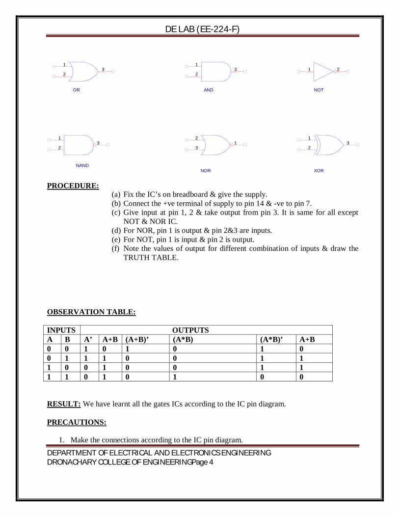
AIM: INTRODUCTION TO DIGITAL ELECTRONICS LAB- NOMENCLATURE OF DIGITAL ICS, SPECIFICATIONS, STUDY OF THE DATA SHEET, CONCEPT OF VCC AND GROUND, VERIFICATION OF THE TRUTH TABLES OF LOGIC GATES USING TTL ICS. APPARATUS REQUIRED: Power Supply, Digital Trainer Kit., Connecting Leads, IC’s (7400, 7402, 7404, 7408, 7432, 7486) BRIEF THEORY: AND Gate: The AND operation is defined as the output as one if and only if all the inputs are one. 7408 is the two Input AND gate IC.A&B are the Input terminals &Y is the Output terminal. Y = A.B OR Gate: The OR operation is defined as the output as one if one or more than o inputs are one. 7432 is the two Input OR gate IC. A&B are the input terminals & Y is the Output terminal. Y = A + B NOT GATE: The NOT gate is also known as Inverter. It has one input (A) & one output (Y). IC No. is 7404. Its logical equation is, Y = A NOT B, Y = A’ NAND GATE: The IC no. for NAND gate is 7400. The NOT-AND operation is known as NAND operation. If all inputs are 1 then output produced is 0. NAND gate is inverted AND gate. Y = A. B NOR GATE: The NOR gate has two or more input signals but only one output signal. IC 7402 istwo I/P IC. The NOT- OR operation is known as NOR operation. If all the inputs are 0 then the O/P is 1. NOR gate is inverted OR gate.
Y = A + B EX-OR GATE: The EX-OR gate can have two or more inputs but produce one output. 7486 is two input IC. EX-OR gate is not a basic operation & can be performed using basic gates. Y = A+ B CIRCUIT DIAGRAM:
DE LAB (EE-224-F)
DEPARTMENT OF ELECTRICAL AND ELECTRONICS ENGINEERING DRONACHARY COLLEGE OF ENGINEERINGPage 4
PROCEDURE:
(a) Fix the IC’s on breadboard & give the supply. (b) Connect the +ve terminal of supply to pin 14 & -ve to pin 7. (c) Give input at pin 1, 2 & take output from pin 3. It is same for all except
NOT & NOR IC. (d) For NOR, pin 1 is output & pin 2&3 are inputs. (e) For NOT, pin 1 is input & pin 2 is output. (f) Note the values of output for different combination of inputs & draw the
TRUTH TABLE.
OBSERVATION TABLE: INPUTS OUTPUTS A B A’ A+B (A+B)’ (A*B) (A*B)’ A+B 0 0 1 0 1 0 1 0 0 1 1 1 0 0 1 1 1 0 0 1 0 0 1 1 1 1 0 1 0 1 0 0 RESULT: We have learnt all the gates ICs according to the IC pin diagram. PRECAUTIONS:
1. Make the connections according to the IC pin diagram.
AND
31 2
3
1
2
3
1
2
NOT
21
OR
31
2
1
2 3
NANDNOR XOR

DE LAB (EE-224-F)
DEPARTMENT OF ELECTRICAL AND ELECTRONICS ENGINEERING DRONACHARY COLLEGE OF ENGINEERINGPage 5
2. The connections should be tight. 3. The Vcc and ground should be applied carefully at the specified pin only.
QUIZ:
QUESTION ANSWER Q.1 Define gates ? A1. Gates are the digital circuits, which
perform a specific type of logical operation
Q.2 Define IC ? A2. IC means integrated circuit. It is the integration of no. of components on a common substrate.
Q.3 Explain Demorgan’s theorem. A3. (AB)’=A’+B’ (A+B)’=A’.B’
Q.4 (A+A) A = ? A4. A
Q5 Define Universal gates. A5. Universal gates are those gates by
using which we can design any type of logical expression.
Q6.Write the logical equation for AND gate. A6.Y=A.B
Q7 How many no. of input variables can a NOT Gate have?
A7. One
Q8.Under what conditions the output of a two input AND gate is one?
A8. Both the inputs are one
Q9.1+0 =? A9. 1 Q10.When will the output of a NAND Gate be 0 ? A10. When all the inputs are 1.

DE LAB (EE-224-F)
DEPARTMENT OF ELECTRICAL AND ELECTRONICS ENGINEERING DRONACHARY COLLEGE OF ENGINEERINGPage 6
EXPERIMENT NO: 2
AIM: IMPLEMENTATION OF THE GIVEN BOOLEAN FUNCTION USING LOGIC GATES IN BOTH SOP AND POS FORMS. APPARATUS REQUIRED: Power Supply, Digital Trainer, IC’s (7404, 7408, 7432) Connecting leads. BRIEF THEORY: Karnaugh maps are perhaps the most extensively used tool for simplification of Boolean functions. It is mostly used for functions having up to six variables beyond which it becomes very cumbersome. In an n-variable K-map there are 2ⁿ cells. Each cell corresponds to one of the combination of n variable, since there are 2ⁿ combinations of n-variables. Gray code has been used for the identification of cells. Example- f(A,B,C,D)=A’BC+AB’C+ABC’+ABC (SOP) Reduced form is BC+AC+ABand POS form is f(X,Y,Z)= Y’(X’+Y+Z’)(X+Z) CIRCUIT DIAGRAM
SOP form POS form
DE LAB (EE-224-F)
DEPARTMENT OF ELECTRICAL AND ELECTRONICS ENGINEERING DRONACHARY COLLEGE OF ENGINEERINGPage 7
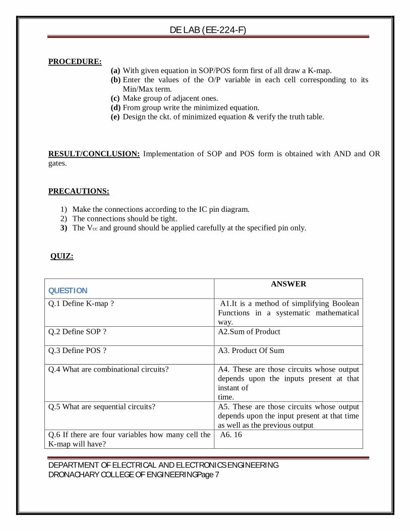
PROCEDURE:
(a) With given equation in SOP/POS form first of all draw a K-map. (b) Enter the values of the O/P variable in each cell corresponding to its
Min/Max term. (c) Make group of adjacent ones. (d) From group write the minimized equation. (e) Design the ckt. of minimized equation & verify the truth table.
RESULT/CONCLUSION: Implementation of SOP and POS form is obtained with AND and OR gates. PRECAUTIONS:
1) Make the connections according to the IC pin diagram. 2) The connections should be tight. 3) The Vcc and ground should be applied carefully at the specified pin only.
QUIZ:
QUESTION ANSWER
Q.1 Define K-map ? A1.It is a method of simplifying Boolean Functions in a systematic mathematical way.
Q.2 Define SOP ? A2.Sum of Product
Q.3 Define POS ? A3. Product Of Sum
Q.4 What are combinational circuits? A4. These are those circuits whose output depends upon the inputs present at that instant of time.
Q.5 What are sequential circuits? A5. These are those circuits whose output depends upon the input present at that time as well as the previous output
Q.6 If there are four variables how many cell the K-map will have?
A6. 16

DE LAB (EE-224-F)
DEPARTMENT OF ELECTRICAL AND ELECTRONICS ENGINEERING DRONACHARY COLLEGE OF ENGINEERINGPage 8
Q.7 When two minterms can be adjacent? A7. 2 to the power n
Q.8 Which code is used for the identification of cells?
A8. Gray Code
Q.9 Define Byte? A9. Byte is a combination of 8 bits.
Q.10 Define octets? A10. It is the combination of 8 K map cells
.

DE LAB (EE-224-F)
DEPARTMENT OF ELECTRICAL AND ELECTRONICS ENGINEERING DRONACHARY COLLEGE OF ENGINEERINGPage 9
EXPERIMENT NO: 3
AIM: VERIFICATION OF STATE TABLES OF RS, JK, T AND D FLIP-FLOPS USING NAND & NOR GATES APPARATUS REQUIRED: IC’ S 7400, 7402 Digital Trainer & Connecting leads. BRIEF THEORY:
RS FLIP-FLOP: There are two inputs to the flip-flop defined as R and S. When I/Ps R = 0 and S = 0 then O/P remains unchanged. When I/Ps R = 0 and S = 1 the flip-flop is switches to the stable state where O/P is 1 i.e. SET. The I/P condition is R = 1 and S = 0 the flip-flop is switched to the stable state where O/P is 0 i.e. RESET. The I/P condition is R = 1 and S = 1 the flip-flop is switched to the stable state where O/P is forbidden.
JK FLIP-FLOP: For purpose of counting, the JK flip-flop is the ideal element to use. The
variable J and K are called control I/Ps because they determine what the flip- flop does when a positive edge arrives. When J and K are both 0s, both AND gates are disabled and Q retains its last value.
• D FLIP –FLOP: This kind of flip flop prevents the value of D from reaching the Q output until a clock pulse occur. When the clock is low, both AND gates are disabled D can change value without affecting the value of Q. On the other hand, when the clock is high, both AND gates are enabled. In this case, Q is forced to equal the value of D. When the clock again goes low, Q retains or stores the last value of D. a D flip flop is a bistable circuit whose D input is transferred to the output after a clock pulse is received.
• T FLIP-FLOP: The T or "toggle" flip-flop changes its output on each clock edge, giving an output which is half the frequency of the signal to the T input. It is useful for constructing binary counters, frequency dividers, and general binary addition devices. It can be made from a J-K flip-flop by tying both of its inputs high.

DE LAB (EE-224-F)
DEPARTMENT OF ELECTRICAL AND ELECTRONICS ENGINEERING DRONACHARY COLLEGE OF ENGINEERINGPage 10
CIRCUIT DIAGRAM:
JK FLIPFLOP T FLIPFLOP PROCEDURE:
1. Connect the circuit as shown in figure. 2. Apply Vcc & ground signal to every IC. 3. Observe the input & output according to the truth table.
OBSERVATION TABLE: SR FLIP FLOP: CLOCK S R Qn+1 1 0 0 NO CHANGE
G1
R6 4
5 64
5
_Q
D
S
3 1 2
31
2
SR FLIPFLOP
Q
CLOCK S-R FLIPFLOP
2 1 G2
Q
_ Q
D FLIPFLOP
CLK
G3
G4

DE LAB (EE-224-F)
DEPARTMENT OF ELECTRICAL AND ELECTRONICS ENGINEERING DRONACHARY COLLEGE OF ENGINEERINGPage 11
1 0 1 0 1 1 0 1 1 1 1 ? D FLIPFLOP: INPUT OUTPUT 0 0 1 1 JK FLIPFLOP CLOCK S R Qn+1 1 0 0 NO CHANGE 1 0 1 0 1 1 0 1 1 1 1 Qn’ T FLIPFLOP CLOCK S R Qn+1 1 0 1 NO CHANGE 1 1 0 Qn’ RESULT: Truth table is verified on digital trainer. PRECAUTIONS:
1) Make the connections according to the IC pin diagram. 2) The connections should be tight. 3) The Vcc and ground should be applied carefully at the specified pin only.
QUIZ: Q 1.Flip flop is astable or bistable? A1.Bistable
Q2.What are the I/Ps of JK flip–flop where this race round condition occurs?
A2.Both the inputs are 1.
Q3.When RS flip-flop is said to be in a SET state?
A3. When the output is 1
Q4.When RS flip-flop is said to be in a RESET A4.When the output is 0

DE LAB (EE-224-F)
DEPARTMENT OF ELECTRICAL AND ELECTRONICS ENGINEERING DRONACHARY COLLEGE OF ENGINEERINGPage 12
state? Q5.What is the truth table of JK flip-flop? J K Qn+1
0 0 Qn
0 1 0 1 0 1 1 1 Qn,
’
Q6.What is the function of clock signal in flip-flop?
A6.To get the output at known time.
Q7.What is the advantage of JK flip-flop over RS flip-flop?
A7.In RS flip-flop when both the inputs are 1 output is undetermined.
Q8.In D flip-flop I/P = 0 what is O/P? A8.0
Q9.In D flip-flop I/P = 1 what is O/P? A9.1
Q10.In T flip-flop I/P = 1 what is O/P? A10.Qn

DE LAB (EE-224-F)
DEPARTMENT OF ELECTRICAL AND ELECTRONICS ENGINEERING DRONACHARY COLLEGE OF ENGINEERINGPage 13
EXPERIMENT NO:4
AIM: IMPLEMENTATION AND VERIFICATION OF DECODER/DE-MULTIPLEXER AND ENCODER USING LOGIC GATES.
APPARATUS REQUIRED: IC 7447, 7-segment display, IC 74139 and connecting leads
BRIEF THEORY:
DECODER:_A decoder is a device which does the reverse of an encoder, undoing the encoding so that the original information can be retrieved. The same method used to encode is usually just reversed in order to decode. In digital electronics, a decoder can take the form of a multiple-input, multiple-output logic circuit that converts coded inputs into coded outputs, where the input and output codes are different. e.g. n-to-2n, binary-coded decimal decoders. Enable inputs must be on for the decoder to function, otherwise its outputs assume a single "disabled" output code word. In case of decoding all combinations of three bits eight (23=8) decoding gates are required. This type of decoder is called 3-8 decoder because 3 inputs and 8 outputs . For any input combination decoder outputs are 1 .
ENCODER : An encoder is a device, circuit, transducer, software program, algorithm or person that converts information from one format or code to another, for the purposes of standardization, speed, secrecy, security, or saving space by shrinking size. An encoder has M input and N output lines. Out of M input lines only one is activated at a time and produces equivalent code on output N lines. If a device output code has fewer bits than the input code has, the device is usually called an encoder. For example Octal-to-Binary Encoder take 8 inputs and provides 3 outputs, thus doing the opposite of what the 3-to-8 decoder does. At any one time, only one input line has a value of 1. The figure below shows the truth table of an Octal-to-binary encoder.
For an 8-to-3 binary encoder with inputs I0-I7 the logic expressions of the outputs Y0-Y2 are:
Y0 = I1 + I3 + I5 + I7 Y1= I2 + I3 + I6 + I7 Y2 = I4 + I5 + I6 +I7
DEMULTIPLEXER: Demultiplexer means generally one into many. A demultiplexer is a logic circuit with one input and many output. By applying control signals, We can steer the input signal to one of the output lines. The ckt. has one input signal, m control signal and n output signals. Where 2n = m. It functions as an electronic switch to route an incoming data signal to one of several outputs.

DE LAB (EE-224-F)
DEPARTMENT OF ELECTRICAL AND ELECTRONICS ENGINEERING DRONACHARY COLLEGE OF ENGINEERINGPage 14
CIRCUIT DIAGRAM:
3:8 Decoder

DE LAB (EE-224-F)
DEPARTMENT OF ELECTRICAL AND ELECTRONICS ENGINEERING DRONACHARY COLLEGE OF ENGINEERINGPage 15
Octal to Binary Encoder
1:4 Demux
PROCEDURE:
1) Connect the circuit as shown in figure. 2) Apply Vcc & ground signal to every IC. 3) Observe the input & output according to the truth table.
OBSERVATION TABLE:

DE LAB (EE-224-F)
DEPARTMENT OF ELECTRICAL AND ELECTRONICS ENGINEERING DRONACHARY COLLEGE OF ENGINEERINGPage 16
Truth table for Decoder
Truth table for Encoder
Truth table for Demux
RESULT: Encoder/ decoder and demultiplexer have been studied and verified. PRECAUTIONS:
DE LAB (EE-224-F)
DEPARTMENT OF ELECTRICAL AND ELECTRONICS ENGINEERING DRONACHARY COLLEGE OF ENGINEERINGPage 17
1) Make the connections according to the IC pin diagram. 2) The connections should be tight. 3) The Vcc and ground should be applied carefully at the specified pin only.
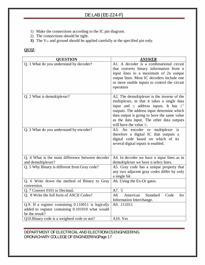
QUIZ:
QUESTION ANSWER Q. 1 What do you understand by decoder? A1. A decoder is a combinational circuit
that converts binary information from n input lines to a maximum of 2n unique output lines. Most IC decoders include one or more enable inputs to control the circuit operation
Q. 2 What is demultiplexer? A2. The demultiplexer is the inverse of the multiplexer, in that it takes a single data input and n address inputs. It has 2n outputs. The address input determine which data output is going to have the same value as the data input. The other data outputs will have the value 0.
Q. 3 What do you understand by encoder? A3. An encoder or multiplexer is therefore a digital IC that outputs a digital code based on which of its several digital inputs is enabled.
Q. 4 What is the main difference between decoder and demultiplexer?
A4. In decoder we have n input lines as in demultiplexer we have n select lines.
Q. 5 Why Binary is different from Gray code? A5. Gray code has a unique property that any two adjacent gray codes differ by only a single bit.
Q. 6 Write down the method of Binary to Gray conversion.
A6. Using the Ex-Or gates.
Q. 7 Convert 0101 to Decimal. A7. 5 Q. 8 Write the full form of ASCII Codes? A8. American Standard Code for
Information Interchange. Q.9. If a register containing 0.110011 is logically added to register containing 0.101010 what would be the result?
A9. .111011
Q10.Binary code is a weighted code or not? A10. Yes

DE LAB (EE-224-F)
DEPARTMENT OF ELECTRICAL AND ELECTRONICS ENGINEERING DRONACHARY COLLEGE OF ENGINEERINGPage 18
EXPERIMENT NO : 5
AIM: IMPLEMENTATION OF 4X1 MULTIPLEXER USING LOGIC GATES. APPARATUS REQUIRED: Power Supply, Digital Trainer, Connecting Leads, IC’s 74153(4x1 multiplexer ) BRIEF THEORY: MULTIPLEXER: Multiplexer generally means many into one. A multiplexer is a circuit with many Inputs but only one output . By applying control signals we can steer any input to the output .The fig.(1) Shows the general idea . The ckt. has n-input signal, control signal & one output signal . Where 2n = m . One of the popular multiplexer is the 16 to 1 multiplexer, which has 16 input bits, 4 control bits & 1 output bit. CIRCUIT DIAGRAM:
IC 74153 (4x1 multiplexer)

DE LAB (EE-224-F)
DEPARTMENT OF ELECTRICAL AND ELECTRONICS ENGINEERING DRONACHARY COLLEGE OF ENGINEERINGPage 19
PROCEDURE: 1. Fix the IC's on the bread board &give the input supply. 2. Make connection according to the circuit. 3. Give select signal and strobe signal at respective pins. 4. Connect +5 v Vcc supply at pin no 24 & GND at pin no 12 5. Verify the truth table for various inputs.
OBSERVATION TABLE:

DE LAB (EE-224-F)
DEPARTMENT OF ELECTRICAL AND ELECTRONICS ENGINEERING DRONACHARY COLLEGE OF ENGINEERINGPage 20
Truth Table of multiplexer (4x1) IC 74153 RESULT: Verify the truth table of multiplexer for various inputs. PRECAUTIONS:
1) Make the connections according to the IC pin diagram. 2) The connections should be tight. 3) The Vcc and ground should be applied carefully at the specified pin only.
QUIZ:
QUESTION ANSWER
Q.1 Why is MUX called as “ Data Selector” ? A1. This selects one out of many inputs. Q.2 What do you mean by Multiplexing? A2. Multiplexing means selecting only a
single input out of many inputs. Q.3 What is Digital Multiplexer? A3. The multiplexer which acts on digital
data. Q.4 What is the function of Enable input to any IC ?
A4. When this enable signal is activated only then the output will be enabled.
Q.5 What is demultiplexer? A5. A demultiplexer transmits the data from a single source to various sources.
Q.6 Can a decoder function as a D’MUX? A6. Yes Q.7 What is the role of select lines in a Demultiplexer?
A7. Select line selects the output line.
Q.8 Differentiate between functions of MUX & D’MUX?
A8. Multiplexer has only single output but demultiplexer has many outputs
Q.9 The number of control lines required for a 1:8 demultiplexer will be
A9. 3
Q.10 How many 4:1 multiplexers will be required to design 8:1 multiplexer?
A10. 2

DE LAB (EE-224-F)
DEPARTMENT OF ELECTRICAL AND ELECTRONICS ENGINEERING DRONACHARY COLLEGE OF ENGINEERINGPage 21
EXPERIMENT NO - 6 AIM – IMPLEMENTATION OF 4-BIT PARALLEL ADDER USING 7483 IC. APPRATUS REQUIRED – Digital trainer kit IC 7483 (4-bit parallel adder) BRIEF THEORY :- An 4-bit adder is a circuit which adds two 4-bits numbers, say, A and B. In addition, an 4-bit adder will have another single-bit input which is added to the two numbers called the carry-in (Cin). The output of the 4-bit adder is an 4-bit sum (S) and a carry-out (Cout) bit. CIRCUIT DIAGRAM :-
7483 4-bit Parallel Adder

DE LAB (EE-224-F)
DEPARTMENT OF ELECTRICAL AND ELECTRONICS ENGINEERING DRONACHARY COLLEGE OF ENGINEERINGPage 22
TRUTH TABLE –
PROCEDURE –
a) Make the connections as per the logic diagram b) Connect +5v and ground according to pin configuration c) Apply diff combinations of inputs to the i/p terminals. d) Note o/p for summation e) Verify the truth table.
RESULT- Binary 4-bit full adder is studied and verified. PRECAUTIONS:
1. Make the connections according to the IC pin diagram. 2. The connections should be tight. 3. The Vcc and ground should be applied carefully at the specified pin only.

DE LAB (EE-224-F)
DEPARTMENT OF ELECTRICAL AND ELECTRONICS ENGINEERING DRONACHARY COLLEGE OF ENGINEERINGPage 23
QUIZ QUESTION ANSWER
Q 1 What do you understand by parallel adder?
A If we place full adders in parallel, we can add two- or four-digit numbers or any other size desired i.e known as parallel adder.
Q2 What happens when an N-bit adder adds two numbers whose sum is greater than or equal to 2N
A Overflow
Q3 Is Excess-3 code is weighted code or not?
A Excess-3 is not a weighted code.
Q4 What is IC no. of parallel adder? A IC 7483 Q5 What is the difference between Excess-3 & Natural BCD code?
A Natural BCD code is weighted code but Excess-3 code is not weighted code.
Q6. What is the Excess-3 code for (396)10 A. (396)10 = (011011001001)EX-3 Q7 Can we obtain 1’s complement using parallel adder?
A Yes
Q8 Can we obtain 2’s complement using parallel adder?
A yes
Q9 How many bits can be added using IC7483 parallel adder?
A 4 bits
Q10 Can you obtain subtractor using parallel adder?
A Yes
DE LAB (EE-224-F)
DEPARTMENT OF ELECTRICAL AND ELECTRONICS ENGINEERING DRONACHARY COLLEGE OF ENGINEERINGPage 24
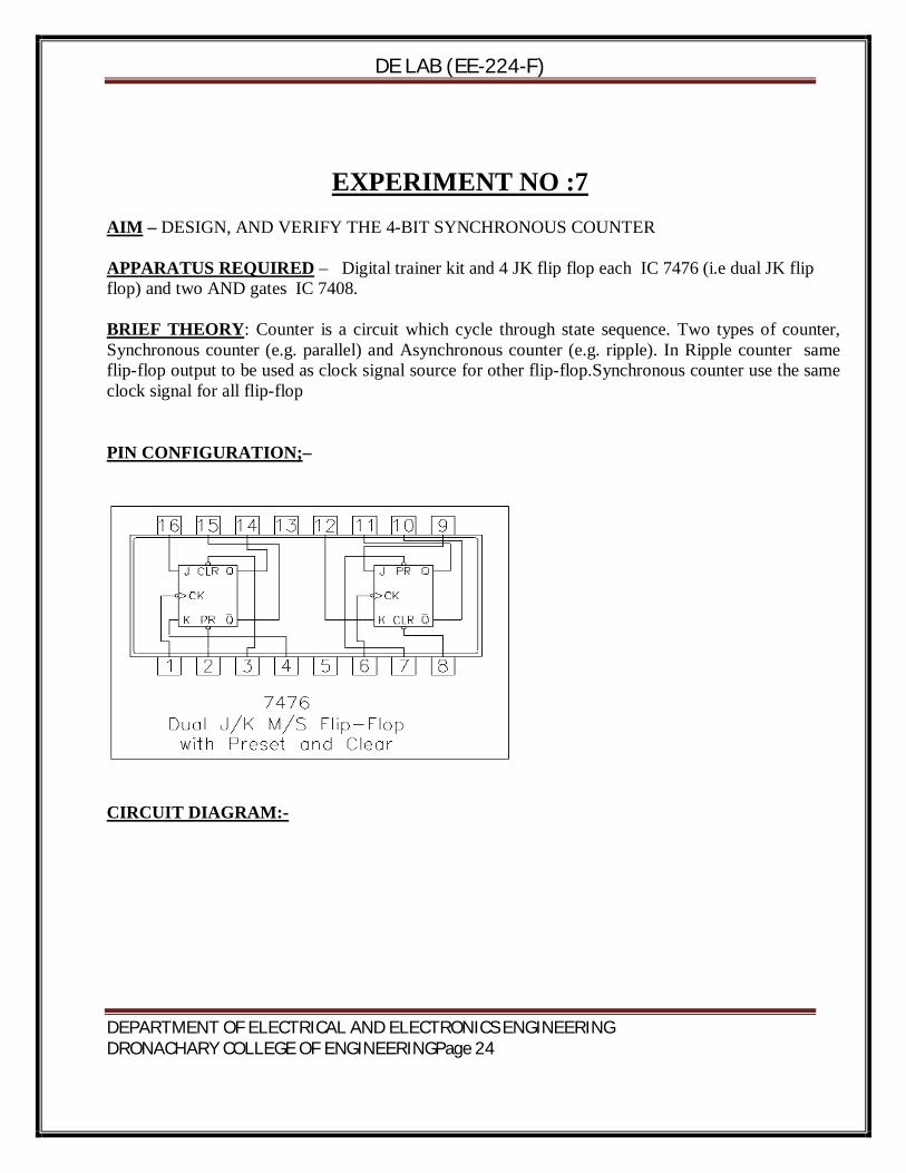
EXPERIMENT NO :7 AIM – DESIGN, AND VERIFY THE 4-BIT SYNCHRONOUS COUNTER APPARATUS REQUIRED – Digital trainer kit and 4 JK flip flop each IC 7476 (i.e dual JK flip flop) and two AND gates IC 7408. BRIEF THEORY: Counter is a circuit which cycle through state sequence. Two types of counter, Synchronous counter (e.g. parallel) and Asynchronous counter (e.g. ripple). In Ripple counter same flip-flop output to be used as clock signal source for other flip-flop.Synchronous counter use the same clock signal for all flip-flop PIN CONFIGURATION;–
CIRCUIT DIAGRAM:-

DE LAB (EE-224-F)
DEPARTMENT OF ELECTRICAL AND ELECTRONICS ENGINEERING DRONACHARY COLLEGE OF ENGINEERINGPage 25
4-Bit Synchronous counter
Pin Number Description
1 Clock 1 Input 2 Preset 1 Input
3 Clear 1 Input 4 J1 Input
5 Vcc 6 Clock 2 Input
7 Preset 2 Input 8 Clear 2 Input
9 J2 Input 10 Complement Q2 Output
11 Q2 Output

DE LAB (EE-224-F)
DEPARTMENT OF ELECTRICAL AND ELECTRONICS ENGINEERING DRONACHARY COLLEGE OF ENGINEERINGPage 26
TRUTH TABLE –
States Count
04 03 02 01
0 0 0 0 0
0 0 0 1 1
0 0 1 0 2
0 0 1 1 3
0 1 0 0 4
0 1 0 1 5
0 1 1 0 6
0 1 1 1 7
1 0 0 0 8
1 0 0 1 9
1 0 1 0 10
1 0 1 1 11
1 1 0 0 12
12 K2 Input
13 Ground 14 Complement Q1 Output
15 Q1 Output 16 K1 Input

DE LAB (EE-224-F)
DEPARTMENT OF ELECTRICAL AND ELECTRONICS ENGINEERING DRONACHARY COLLEGE OF ENGINEERINGPage 27
1 1 0 1 13
1 1 1 0 14
1 1 1 1 15
PROCEDURE –
a) Make the connections as per the logic diagram b) Connect +5v and ground according to pin configuration c) Apply diff combinations of inputs to the i/p terminals. d) Note o/p for summation e) Verify the truth table.
RESULT- 4-bit synchronous counter studied and verified. PRECAUTIONS:
1. Make the connections according to the IC pin diagram. 2. The connections should be tight. 3. The Vcc and ground should be applied carefully at the specified pin only.
QUIZ QUESTION ANSWER
Q.1 What do you understand by counter? A. Counter is a register which counts the
sequence in binary form.
Q.2What is asynchronous counter? A. Clock input is applied to LSB FF. The output of first FF is connected as clock to next FF
Q.3What is synchronous counter? A. WhereClock input is common to all FF
Q.4Which flip flop is used in asynchronous counter?
A. All Flip-Flops are toggle FF.
Q.5Which flip flop is used in synchronous A. Any FF can be used.

DE LAB (EE-224-F)
DEPARTMENT OF ELECTRICAL AND ELECTRONICS ENGINEERING DRONACHARY COLLEGE OF ENGINEERINGPage 28
counter? Q.6 What do you understand by modulus? A. The total no. of states in counter is
called as modulus.If counter is modulus-n, then it has n different states
Q.7 What do you understand by state diagram?
A. State diagram of counter is a pictorial representation of counter states directed by arrows in graph
Q.8 What do you understand by up/down counter?
A. Up/Down Synchronous Counter: two way counter which able to count up or down
Q.9 Why Asynchronous counter is known as ripple counter ?
A. Asynchronous Counter : flip-flop doesn’t change condition simultaneously because it doesn’t use single clock signalAlso known as ripple counter because clock signal input as ripple through counter
Q.10 which type of counter is used in traffic signal?
A. Down counter

DE LAB (EE-224-F)
DEPARTMENT OF ELECTRICAL AND ELECTRONICS ENGINEERING DRONACHARY COLLEGE OF ENGINEERINGPage 29
EXPERIMENT NO :8 AIM – DESIGN, AND VERIFY THE 4-BIT ASYNCHRONOUS COUNTER APPARATUS REQUIRED – Digital trainer kit and 4 JK flip flop each IC 7476 (i.e dual JK flip flop) and two AND gates IC 7408. BRIEF THEORY: Counter is a circuit which cycle through state sequence. Two types of counter, Synchronous counter (e.g. parallel) and Asynchronous counter (e.g. ripple). In Ripple counter same flip-flop output to be used as clock signal source for other flip-flop.Synchronous counter use the same clock signal for all flip-flop PIN CONFIGURATION;–
CIRCUIT DIAGRAM

DE LAB (EE-224-F)
DEPARTMENT OF ELECTRICAL AND ELECTRONICS ENGINEERING DRONACHARY COLLEGE OF ENGINEERINGPage 30
PROCEDURE –
a)Make the connections as per the logic diagram b)Connect +5v and ground according to pin configuration c)Apply diff combinations of inputs to the i/p terminals. d)Note o/p for summation e)Verify the truth table.
RESULT- 4-bit asynchronous counter studied and verified.
Pin Number Description
1 Clock 1 Input 2 Preset 1 Input
3 Clear 1 Input 4 J1 Input
5 Vcc 6 Clock 2 Input
7 Preset 2 Input
8 Clear 2 Input 9 J2 Input
10 Complement Q2 Output 11 Q2 Output
12 K2 Input 13 Ground
14 Complement Q1 Output 15 Q1 Output
16 K1 Input

DE LAB (EE-224-F)
DEPARTMENT OF ELECTRICAL AND ELECTRONICS ENGINEERING DRONACHARY COLLEGE OF ENGINEERINGPage 31
PRECAUTIONS:
4. Make the connections according to the IC pin diagram. 5. The connections should be tight. 6. The Vcc and ground should be applied carefully at the specified pin only.

DE LAB (EE-224-F)
DEPARTMENT OF ELECTRICAL AND ELECTRONICS ENGINEERING DRONACHARY COLLEGE OF ENGINEERINGPage 32
EXPERIMENT NO:9
AIM – TO STUDY 4 BIT SERIAL IN SHIFT REGISTER. APPARATUS REQUIRED – Digital trainer kit and IC -7494,74164,74165,74166 BRIEF THEORY - Register in which data are entered or/and taken out in serial form are referred to as shift register, since bits are shifted in the FLIP_FLOPS with the occurrence of clock pulses either in the right direction or in the left direction. In the bi-directional shift register, data can be shifted from left to right as in the reverse direction, using the mode control. Shift Register are capable of storing and shifting the data. They are classified as- 1. Serial in Serial out 2. Serial in Parallel out 3. Parallel in Serial out 4. Parallel in Parallel out A 5-bit shift register using 5 master-slave S-R(or J-K) FLIP-FLOP. This ckt can be used in any of four modes. The operation is explained by assuming the 5-bit data 10110.

DE LAB (EE-224-F)
DEPARTMENT OF ELECTRICAL AND ELECTRONICS ENGINEERING DRONACHARY COLLEGE OF ENGINEERINGPage 33

DE LAB (EE-224-F)
DEPARTMENT OF ELECTRICAL AND ELECTRONICS ENGINEERING DRONACHARY COLLEGE OF ENGINEERINGPage 34
Registers in which data are entered or /and taken out in a serial form are reffered to as Shift register since bits are shifted in the Flip-Flop with the occurrence of clock pluses either in right direction or in the left direction. Data can be shifted from left to right as well as in the reverse direction using the mode control. A register is referred to as Universal register if it can be operated in all the four possible modes and also as a bidirectional register. QUIZ –

DE LAB (EE-224-F)
DEPARTMENT OF ELECTRICAL AND ELECTRONICS ENGINEERING DRONACHARY COLLEGE OF ENGINEERINGPage 35
QUESTION ANSWER
Q1 What is the difference between Register and Shift Register?
A. A Register is used to store an array of bits and SR is used to shift the bits to either left or right.
Q2. Name the various configuration of SR
A. 1. Serial in serial out 2. Serial in parallel out 3. Parallel in serial out 4. Parallel in parallel out
Q3. What is Bidirectional Shift Register? A. Which can shift data in both directions Q4. What is asynchronous loading? A. Data is loaded into register when ‘1’ is
applied at the present input. Q5. What is synchronous loading? A. Data is loaded when a clock pulse is
applied. Q6. What are the applications of Shift Register?
A. a. As delay line b. serial to parallel converter c. parallel to serial converter d. counter
Q7. What is Race condition in Sequential circuit?
A. A Race condition exists when more than one state variable change value in response to a change in an input variable.
Q8. What is Right Shift register? A. Data gets shifted in right direction. Q9. What is Left Shift register? A. Data gets shifted in left direction. Q10. What is Flow table? A. A tabular method for showing state
transaction in assigning sequential circuits.

DE LAB (EE-224-F)
DEPARTMENT OF ELECTRICAL AND ELECTRONICS ENGINEERING DRONACHARY COLLEGE OF ENGINEERINGPage 36
EXPERIMENT NO: 10
AIM: TO DESIGN &VERIFY OPERATION OF HALF ADDER &FULL ADDER. APPARATUS REQUIRED: Power supply, IC’s , Digital Trainer, Connecting leads . BRIEF THEORY: We are familiar with ALU, which performs all arithmetic and logic operation but ALU doesn’t perform/ process decimal no’s. They process binary no’s. Half Adder: It is a logic circuit that adds two bits. It produces the O/P, sum & carry.The Boolean equation for sum & carry are SUM = A + B CARRY = A. B Therefore, sum produces 1 when A&B are different and carry is 1when A&B are 1. Application of Half adder is limited. Full Adder: It is a logic circuit that can add three bits. It produces two O/P sum & carry. The Boolean Equation for sum & carry are
SUM = A + B + C CARRY = A.B + (A+B) C
Therefore, sum produces one when I/P is containing odd no’s of one & carry is one when there are two or more one in I/P.
CIRCUIT DAIGRAM
6 4
5
6 4
5
HALF ADDER
31
2
31 2
3 1
2
31 2
3 1
2
FULL ADDER
DE LAB (EE-224-F)
DEPARTMENT OF ELECTRICAL AND ELECTRONICS ENGINEERING DRONACHARY COLLEGE OF ENGINEERINGPage 37
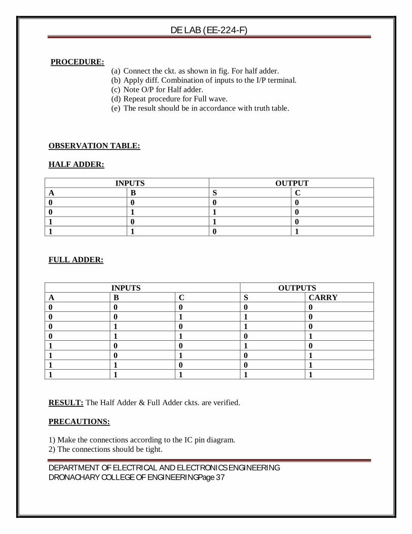
PROCEDURE:
(a) Connect the ckt. as shown in fig. For half adder. (b) Apply diff. Combination of inputs to the I/P terminal. (c) Note O/P for Half adder. (d) Repeat procedure for Full wave. (e) The result should be in accordance with truth table.
OBSERVATION TABLE: HALF ADDER: INPUTS OUTPUT A B S C 0 0 0 0 0 1 1 0 1 0 1 0 1 1 0 1 FULL ADDER: INPUTS OUTPUTS A B C S CARRY 0 0 0 0 0 0 0 1 1 0 0 1 0 1 0 0 1 1 0 1 1 0 0 1 0 1 0 1 0 1 1 1 0 0 1 1 1 1 1 1 RESULT: The Half Adder & Full Adder ckts. are verified. PRECAUTIONS: 1) Make the connections according to the IC pin diagram. 2) The connections should be tight.

DE LAB (EE-224-F)
DEPARTMENT OF ELECTRICAL AND ELECTRONICS ENGINEERING DRONACHARY COLLEGE OF ENGINEERINGPage 38
3) The Vcc and ground should be applied carefully at the specified pin only. QUIZ:
QUESTION ANSWER Q.1 Give the basic rules for binary addition?
A1. 0+0 = 0; 0+1 = 1 ; 1+1 = 1 0 ; 1+0 = 1.
Q.2 Specify the no. of I/P and O/P of Half adder?
A2. Two inputs & one output.
Q.3 What is the drawback of half adder?
A3. We can’t add carry bit from previous stage.
Q.4 Write the equation for sum & carry of half adder?
A4. Sum = A XOR B; carry = A.B
Q.5 Write the equation for sum & carry of full adder?
A5. SUM= A’B’C+A’BC’+AB’C’+ABC; CARRY=AB+BC+AC
Q.6 How many half adders will be required for Implementing full adder?
A6 Two half adders and a OR gate
Q7 Define Bit? A7 Bit is an abbreviation for binary digit Q8.What is the difference b/w half adder& half sub tractor?
A8.Half adder can add two bits & half sub tractor can subtract two bits
Q9. Half sub tractor logic circuit has one extra logic element. Name the element?
A9. Inverter
Q10. Define Nibble? A10.Combination of four bits.

DE LAB (EE-224-F)
DEPARTMENT OF ELECTRICAL AND ELECTRONICS ENGINEERING DRONACHARY COLLEGE OF ENGINEERINGPage 39
EXPERIMENT NO :11
AIM- TO STUDY &VERIFY HALF SUBTRACTOR. APPARATUS REQUIRED – Digital trainer kit, IC 7486 (EX-OR) IC 7408 (AND gate) IC 7404 (NOT gate) BRIEF THEORY - A logic circuit fir the subtraction of B(subtrahend) from A (minuend) where A& B are 1 bit numbers is referred as half- sub tractor. LOGIC DIAGRAM –
TRUTH TABLE – INPUT 1 (X) INPUT 2 (Y) BORROW (B) DIFFERENCE (D) 0 0 0 0 0 1 1 1 1 0 0 1 1 1 0 0
DE LAB (EE-224-F)
DEPARTMENT OF ELECTRICAL AND ELECTRONICS ENGINEERING DRONACHARY COLLEGE OF ENGINEERINGPage 40
PROCEDURE –
1. Make the connections as per the logic diagram 2. Connect +5v to pin 14 & ground to pin 7 3. Apply 0 to input X & Y as per the truth table 4. Switch on the instrument 5. Observe the reading on 8 bits LED display 6. Repeat steps 3 & 5 for different input as per truth table. 7. Verify the truth table.
RESULT – Half sub tractor circuit is studied and verified.
QUIZ
QUESTION ANSWER
1. What is half subs tractor? A. Performs subs traction of two bits. 2. For implementing half subs tractor how many EX-OR, AND gates and Not gates are required
A. One EX-OR, one –AND gate, one- Not gate.
3. What are the logical equations for difference & borrow?
A. D = ĀB +A¯B B = Ā.B
4. How full substractor is different from half subs tractor.
A Full sub tractor performs subtraction of three bits but half subs tractor Performs subtraction of two bits.
5. If inputs of half subs tractor are A=0, and B=1 then Borrow will be ?
A. B=1
6. Is 2’s complement method appropriate for subtraction?
A. 2’s complement method is appropriate method for subtraction.
7. How many bits we use in half subtractor for subtraction?
Aonly two bits
8. Can we use parallel adder for subtraction?
A. We can use parallel adder using 2’s complement method.
9. Which one is better subtractor or parallel adder for subtraction?
A. Parallel adder is the best option using 1’s complement or 2’s complement
10. Which adder is used for addition of BCD numbers?
A. BCD adder

DE LAB (EE-224-F)
DEPARTMENT OF ELECTRICAL AND ELECTRONICS ENGINEERING DRONACHARY COLLEGE OF ENGINEERINGPage 41
EXPERIMENT NO: 12 AIM: TO DESIGN & VERIFY THE OPERATION OF MAGNITUDE COMPARATOR APPARATUS REQUIRED: Power Supply, Digital Trainer Kit., Connecting Leads, IC’s (7404, 7408, 7486) BRIEF THEORY: Comparator compares the value of signal at the input. It can be designed to compare many bits. The adjoining figure shows the block diagram of comparator. Here it receives to two 2-bit numbers at the input & the comparison is at the output. CIRCUIT DIAGRAM: PROCEDURE:
a. Make the connections according to the circuit diagram. b. The output is high if both the inputs are equal. c. Verify the truth table for different values.
OBSERVATION TABLE:
RESULT: The comparator is designed & verified.
P0 Q0 P1 Q1 LOW IF P IS NOT EQUAL TO Q
HIGH IF Q IS EQUAL TO Q
0 0 0 0 HIGH 1 1 0 0 HIGH 0 1 0 1 LOW 1 0 1 0 LOW
21
31
2
31
2
64
543

DE LAB (EE-224-F)
DEPARTMENT OF ELECTRICAL AND ELECTRONICS ENGINEERING DRONACHARY COLLEGE OF ENGINEERINGPage 42
PRECAUTIONS:
1) Make the connections according to the IC pin diagram. 2) The connections should be tight. 3) The Vcc and ground should be applied carefully at the specified pin only.
QUIZ:
QUESTION ANSWER
Q1.What is comparator? A1.Comparator compares the inputs (bits). Q2. What are universal gates? A2. NAND, NOR Q3. What is the full form of BCD? A3. Binary Coded decimal Q4. What is the base of binary number system? A4. 2 Q5. How many bits are there in one byte? A5. 8 Q6. How many digits are there in octal number system?
A6. 8
Q7. What is the binary no. equivalent to decimal no. 20?
A7. 10100
Q8. How decimal no. minus 7 can be represented by 4 bit signed binary no’s?
A8. 1111
Q9.Convert the octal no 67 into binary no.? A9. 110111 Q10.A binary digit is called? A10. Bit

DE LAB (EE-224-F)
DEPARTMENT OF ELECTRICAL AND ELECTRONICS ENGINEERING DRONACHARY COLLEGE OF ENGINEERINGPage 43
EXPERIMENT NO:13
AIM : TO STUDY AND VERIFY NAND AS A UNIVERSAL GATE. APPARATUS REQUIRED – Digital trainer kit IC 7400 (NAND gate) BRIEF THEORY - NAND OR NOR sufficient for the realization of any logic expression., because of this reason, NAND and NOR gates are known as UNIVERSAL gates. LOGIC DIAGRAM –
TRUTH TABLE – NAND GATE AS INVERTER:-The circuit diagram of implementation of NAND gate as inverter.

DE LAB (EE-224-F)
DEPARTMENT OF ELECTRICAL AND ELECTRONICS ENGINEERING DRONACHARY COLLEGE OF ENGINEERINGPage 44
NAND GATE AS AND GATE :- The circuit diagram of implementation of NAND Gate as AND Gate.
A B Y 0 0 0 0 1 0 1 0 0 1 1 1
NAND GATE AS OR GATE :- The circuit diagram of implementation of NAND Gate as OR Gate. PROCEDURE –
1.Make the connections as per the logic diagram 2. Connect +5v to pin 14 & ground to pin 7 3. Apply diff combinations of inputs to the i/p terminals. 4. Note o/p for NAND as universal gate. 5. Verify the truth table.
A Y
0 1
1 0
A B Y 0 0 0 0 1 1 1 0 1 1 1 1

DE LAB (EE-224-F)
DEPARTMENT OF ELECTRICAL AND ELECTRONICS ENGINEERING DRONACHARY COLLEGE OF ENGINEERINGPage 45
QUIZ QUESTION ANSWER
Q.1 Define Gates. Ans. Gates are digital circuit, which
perform a specific type of logical operation.
Q.2 Define IC? Ans. IC means Integrated Circuit It is the integration of no. of components on a common substrate.
Q.3 (A+A) A=? Ans. A. Q.4. Define universal gates Ans. We can design any type of logical
expression by using universal gates. Q.5 Will the output of a NAND Gate be 0. Ans. When all the inputs are1. Q.6 Which IC is used for NAND Gate. Ans. IC 7400. Q.7 Why NAND is called as universal gate.
Ans. Because all gates can be made using circuits.
Q.8 Name any other universal gate. Ans. NOR Gate. Q.9 Which type of TTL gates can drive CMOS Gate.
Ans. TTL with open collector can derive CMOS
Q.10 What is meant by literal? Ans. A logical variable in a complemented or Uncomplemented form is called a literal

DE LAB (EE-224-F)
DEPARTMENT OF ELECTRICAL AND ELECTRONICS ENGINEERING DRONACHARY COLLEGE OF ENGINEERINGPage 46
EXPERIMENT NO:14
LIST OF MINI PROJECTS
1. IR Remote Switch 2. Clap Switch 3. Water-Level Controller 4. LED-Based Message Display 5. Ultra-Bright LED Lamp 6. Ding-Dong BellInfrared Cordless Headphone 7. Mobile Phone Battery Charger 8. Telephone Number Display 9. Automatic Night Lamp With Morning Alarm 10. Three-Colour Display Using Bicolour LEDs 11. Remote-Operated Musical Bell 12. Simple Telephone Ring Tone Generator 13. Anti-Theft Alarm For Bikes 14. Automatic Speed-Controller For Fans and Coolers 15. Digital Stop Watch 16. Power-Supply Failure Alarm 17. DarkRoom Timer 18. Remote-Controlled Power-Off Switch 19. Simple Low-Cost Digital Code Lock 20. Number Guessing Game 21. Fire Alarm Using Thermistor 22. Simple Analogue To Digital Converter 23. PC-Based 7-Segment Rolling Display 24. IR Burglar Deterrent 25. Variable Power Supply Using a Fixed-Voltage Regulator IC 26. Digital Speedometer 27. Heat-Sensitive Switch 28. Fully Automatic Emergency Light 29. Running Message Display 30. School/College Quiz Buzzer 31. Digital Dice With Numeric Display 32. Dancing Lights 33. Ready -To-Use Object Counter Laptop Protector 34. PC Based Digital Clock 35. Fancy Christmas Light

DE LAB (EE-224-F)
DEPARTMENT OF ELECTRICAL AND ELECTRONICS ENGINEERING DRONACHARY COLLEGE OF ENGINEERINGPage 47
AN EXAMPLE AIM :- LIQUID LEVEL ALARM APPARATUS REQUIRED: Components as shown in the circuit diagram( such as 555IC,, soldering iron and solder flux and PCB board
BRIEF THEORY: Here is a simple circuit for (T1 and T2) and two timer 555 ICs (IC1
and IC2). Both IC1 and IC2 are wired in astable multivibrator mode. Timer IC1 produces low frequency, while timer IC2 produces high frequency. As a result, a beeping tone is generated when the liquid tank is full. Initially, when the tank is empty,transistor T1 does not conduct. Consequently, transistor T2 conducts and pin 4 of IC1 is low. This low voltage disables IC1 and it does not oscillate.The low output of IC1 disables IC2 and it does not oscillate. As a result, no sound is heard from the speaker.But when the tank gets filled up,transistor T1 conducts. Consequently,transistor T2 is cut off and pin 4 of IC1 becomes high. This high voltage enables IC1 and it oscillates to produce low frequencies at pin 3. This low-frequency output enables IC2 and it also oscillates to produce high frequencies. As a result, sound is produced from the speaker. Using preset VR1 you can control the volume of the sound from the speaker.The circuit can be powered from a 9V battery or from mains by using a 9V power adaptor CIRCUIT DIAGRAM:

DE LAB (EE-224-F)
DEPARTMENT OF ELECTRICAL AND ELECTRONICS ENGINEERING DRONACHARY COLLEGE OF ENGINEERINGPage 48
PROCEDURE: Assemble the circuit on a general purpose PCB and enclose in a suitable cabinet. Install two water-level probes using metal strips such that one touches the bottom of the tank and the other touches the maximum level of the water in the tank. Interconnect the sensor and the circuit using a flexible wire. PRECAUTIONS: 1) Make the connections according to the Circuit diagram using soldering iron
2) The connections should be tight. 3) The Vcc and ground should be applied carefully at the specified pin only