ECEN 301Discussion #18 – Operational Amplifiers1 DateDayClass No. TitleChaptersHW Due date Lab Due...
40
ECEN 301 Discussion #18 – Operational Amplifiers 1 Date Day Clas s No. Title Chapters HW Due date Lab Due date Exam 3 Nov Mon 18 Operational Amplifiers 8.4 LAB 6 4 Nov Tue 5 Nov Wed 19 Binary Numbers 13.1 – 13.2 6 Nov Thu 7 Nov Fri Recitation HW 8 8 Nov Sat 9 Nov Sun 10 Nov Mon 20 Exam Review LAB 7 EXAM 2 12 Nov Tue Schedule…
-
Upload
tamsin-andrews -
Category
Documents
-
view
214 -
download
0
Transcript of ECEN 301Discussion #18 – Operational Amplifiers1 DateDayClass No. TitleChaptersHW Due date Lab Due...

ECEN 301Discussion #18 – Operational
Amplifiers1
Date Day ClassNo.
Title Chapters HWDue date
LabDue date
Exam
3 Nov Mon 18 Operational Amplifiers
8.4
LAB 6
4 Nov Tue
5 Nov Wed 19 Binary Numbers 13.1 – 13.2
6 Nov Thu
7 Nov Fri Recitation HW 8
8 Nov Sat
9 Nov Sun
10 Nov Mon 20 Exam Review
LAB 7 EXAM 212 Nov Tue
Schedule…
ECEN 301Discussion #18 – Operational
Amplifiers2
Give to ReceiveAlma 34:28 28 And now behold, my beloved brethren, I say unto you, do not
suppose that this is all; for after ye have done all these things, if ye turn away the needy, and the naked, and visit not the sick and afflicted, and impart of your substance, if ye have, to those who stand in need—I say unto you, if ye do not any of these things, behold, your prayer is vain, and availeth you nothing, and ye are as hypocrites who do deny the faith.
ECEN 301Discussion #18 – Operational
Amplifiers3
Lecture 18 – Operational Amplifiers
Answer questions from last lecture
Continue with Different OpAmp configurations
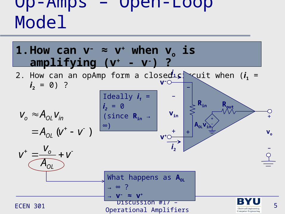
ECEN 301Discussion #17 – Operational
Amplifiers4
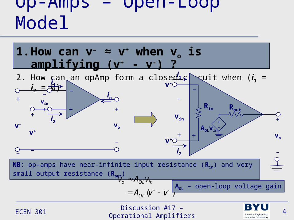
Op-Amps – Open-Loop Model
1. How can v– ≈ v+ when vo is amplifying (v+ - v-) ? 2. How can an opAmp form a closed circuit when (i1 = i2 = 0) ?
–
++
v+
–
+
v–
–
+
vo
–
io
i2
i1–vin
+
–
+
+–
RoutRin
i1
AOLvin
+
vo
–
–
vin
+
v–
v+
NB: op-amps have near-infinite input resistance (Rin) and very small output resistance (Rout)
)(
vvA
vAv
OL
inOLoAOL – open-loop voltage gain
i2
ECEN 301Discussion #17 – Operational
Amplifiers5
Op-Amps – Open-Loop Model
1. How can v– ≈ v+ when vo is amplifying (v+ - v-) ? 2. How can an opAmp form a closed circuit when (i1 = i2 = 0) ?
–
+
+–
RoutRin
i1
AOLvin
+
vo
–
–
vin
+
v–
v+
vA
vv
vvA
vAv
OL
o
OL
inOLo
)(i2
Ideally i1 = i2 = 0(since Rin → ∞)
What happens as AOL → ∞ ?→ v– ≈ v+
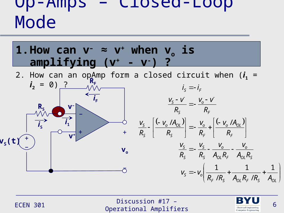
ECEN 301Discussion #17 – Operational
Amplifiers6
Op-Amps – Closed-Loop Mode
RF
–
+ +
vo
–
i1
RS
vS(t)+–
v+
v–
iF
iS
OLSFOLSFoS
SOL
o
FOL
o
S
S
S
S
F
OLo
F
o
S
OLo
S
S
F
o
S
S
FS
ARRARRvv
RA
v
RA
v
R
v
R
v
R
Av
R
v
R
Av
R
v
R
vv
R
vv
ii
1
/
1
/
1
//
1. How can v– ≈ v+ when vo is amplifying (v+ - v-) ? 2. How can an opAmp form a closed circuit when (i1 = i2 = 0) ?
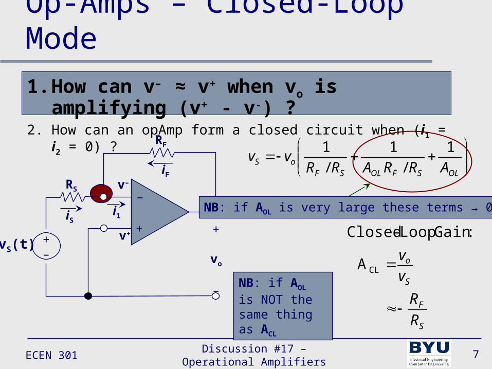
ECEN 301Discussion #17 – Operational
Amplifiers7
Op-Amps – Closed-Loop Mode
OLSFOLSFoS ARRARRvv
1
/
1
/
1RF
–
+ +
vo
–
i1
RS
vS(t)+–
v+
v–
iF
iSNB: if AOL is very large these terms → 0
S
F
S
o
R
R
vv
CLA
:Gain Loop-Closed
NB: if AOL is NOT the same thing as ACL
1. How can v– ≈ v+ when vo is amplifying (v+ - v-) ? 2. How can an opAmp form a closed circuit when (i1 = i2 = 0) ?
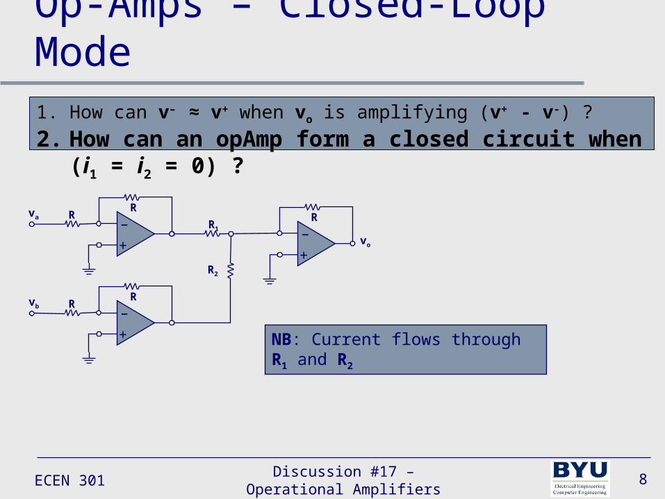
ECEN 301Discussion #17 – Operational
Amplifiers8
Op-Amps – Closed-Loop Mode
–
+
va RR
–
+
vb RR
–
+
R1
R
R2
vo
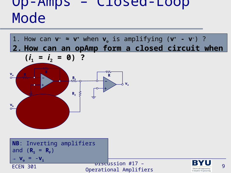
1. How can v– ≈ v+ when vo is amplifying (v+ - v-) ?
2. How can an opAmp form a closed circuit when (i1 = i2 = 0) ?
NB: Current flows through R1 and R2
ECEN 301Discussion #17 – Operational
Amplifiers9
Op-Amps – Closed-Loop Mode
–
+
va RR
–
+
vb RR
–
+
R1
R
R2
vo
1. How can v– ≈ v+ when vo is amplifying (v+ - v-) ?
2. How can an opAmp form a closed circuit when (i1 = i2 = 0) ?
NB: Inverting amplifiers and (RS = RF) → vo = -vi
ECEN 301Discussion #17 – Operational
Amplifiers10
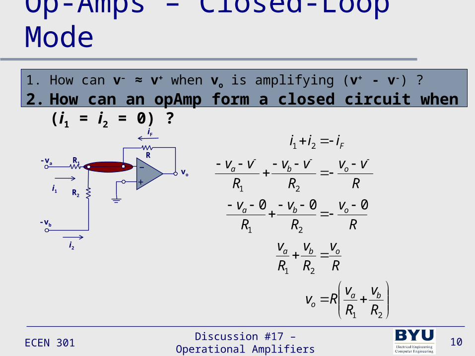
Op-Amps – Closed-Loop Mode1. How can v– ≈ v+ when vo is amplifying (v+ - v-) ?
2. How can an opAmp form a closed circuit when (i1 = i2 = 0) ?
–
+
R1
R
R2
vo
-va
-vb
21
21
21
21
21
000
R
v
R
vRv
R
v
R
v
R
v
R
v
R
v
R
v
R
vv
R
vv
R
vv
iii
bao
oba
oba
oba
F
iF
i1
i2

ECEN 301Discussion #18 – Operational
Amplifiers11
More OpAmp Configurations
ECEN 301Discussion #18 – Operational
Amplifiers12
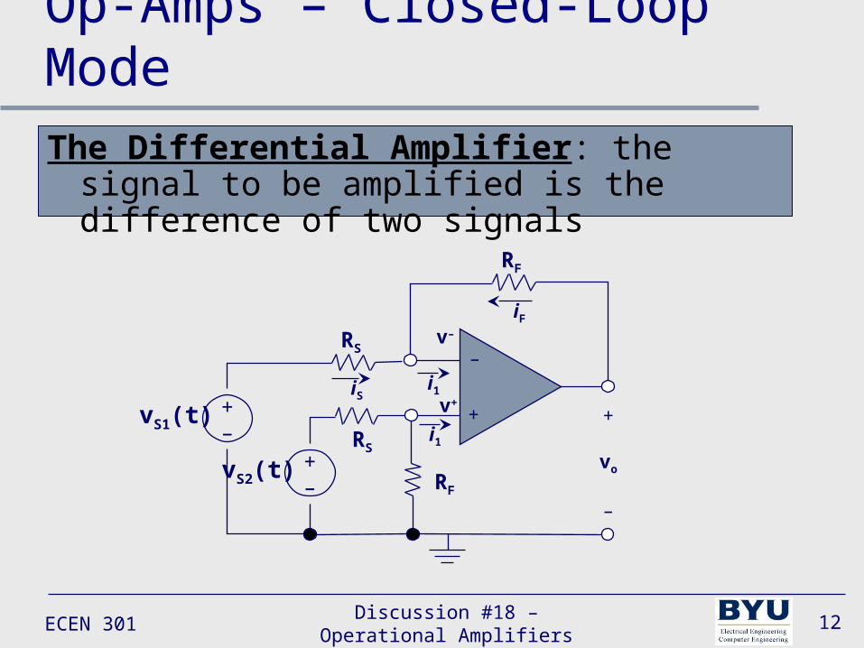
Op-Amps – Closed-Loop Mode
The Differential Amplifier: the signal to be amplified is the difference of two signals
–
+ +
vo
–
i1
RF
vS2(t)+–
v+
v–
iFRS
iS
i1vS1(t)
+–
RF
RS
ECEN 301Discussion #18 – Operational
Amplifiers13
Op-Amps – Closed-Loop Mode
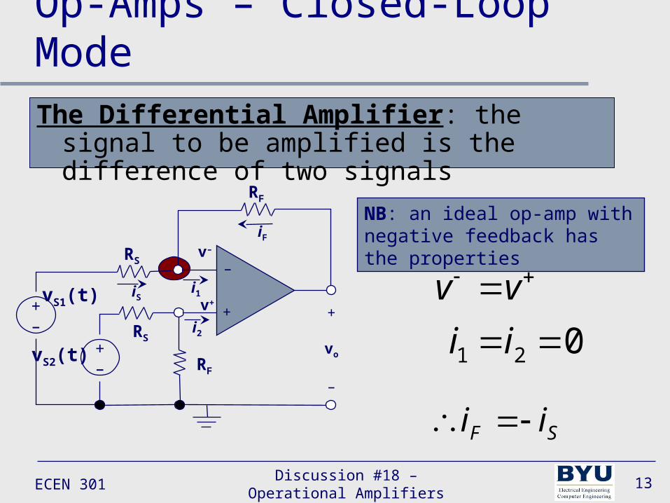
The Differential Amplifier: the signal to be amplified is the difference of two signals
021
ii
vv
RF
–
+ +
vo
–
i1
vS2(t)+–
v+
v–
iFRS
iS
i2
vS1(t)+–
RF
RS
NB: an ideal op-amp with negative feedback has the properties
SF ii
ECEN 301Discussion #18 – Operational
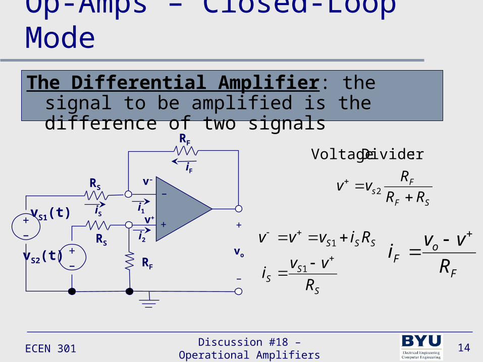
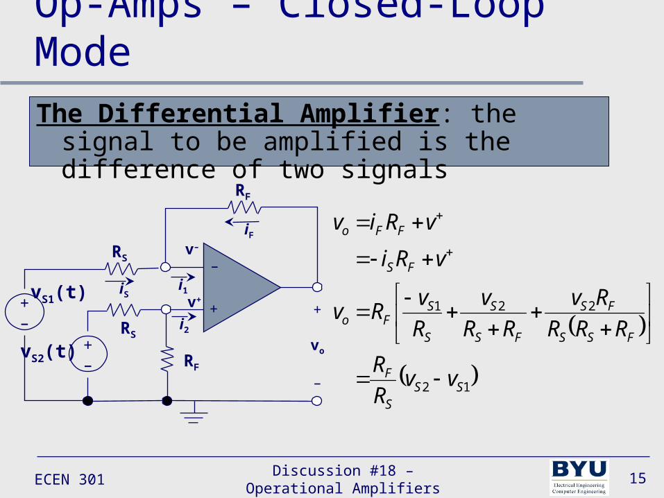
Amplifiers14
Op-Amps – Closed-Loop Mode
The Differential Amplifier: the signal to be amplified is the difference of two signals
SF
Fs RR
Rvv
2
:Divider VoltageRF
–
+ +
vo
–
i1
vS2(t)+–
v+
v–
iFRS
iS
i2
vS1(t)+–
RF
RS
S
SS
SSS
R
vvi
Rivvv
1
1
F
oF R
vvi
ECEN 301Discussion #18 – Operational
Amplifiers15
Op-Amps – Closed-Loop Mode
The Differential Amplifier: the signal to be amplified is the difference of two signals
RF
–
+ +
vo
–
i1
vS2(t)+–
v+
v–
iFRS
iS
i2
vS1(t)+–
RF
RS
12
221
SSS
F
FSS
FS
FS
S
S
SFo
FS
FFo
vvR
R
RRR
Rv
RR
v
R
vRv
vRi
vRiv
ECEN 301Discussion #18 – Operational
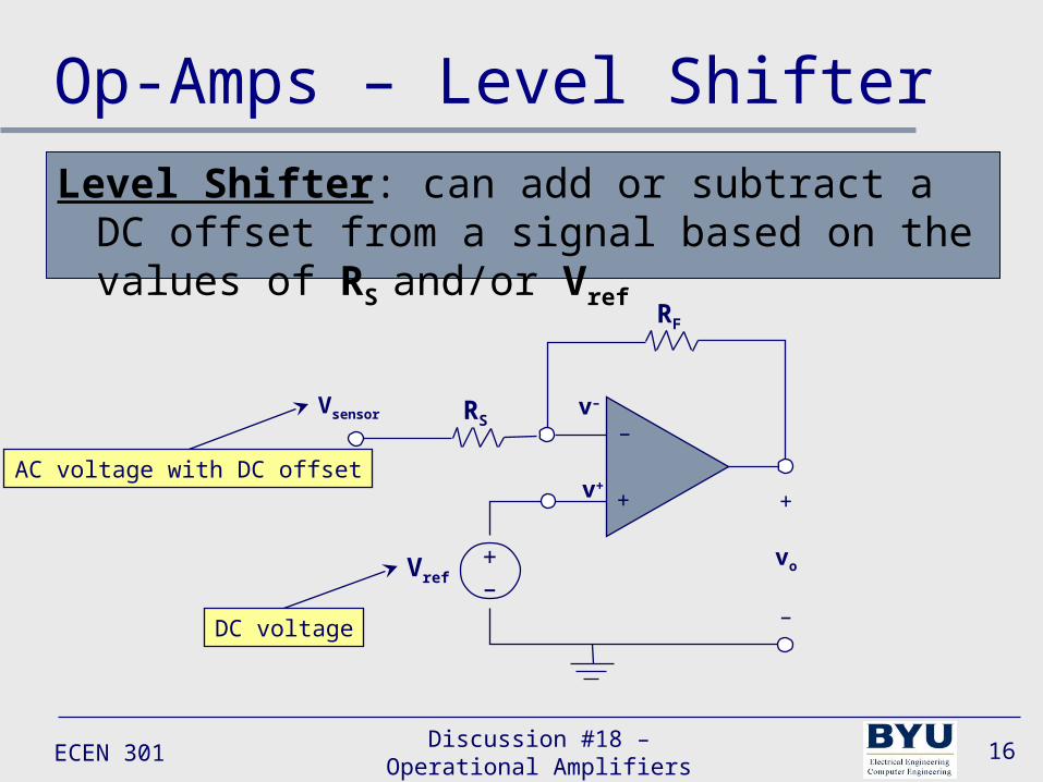
Amplifiers16
Op-Amps – Level Shifter
Level Shifter: can add or subtract a DC offset from a signal based on the values of RS and/or Vref
–
+ +
vo
–
RF
Vref+–
v+
v–RSVsensor
AC voltage with DC offset
DC voltage
ECEN 301Discussion #18 – Operational
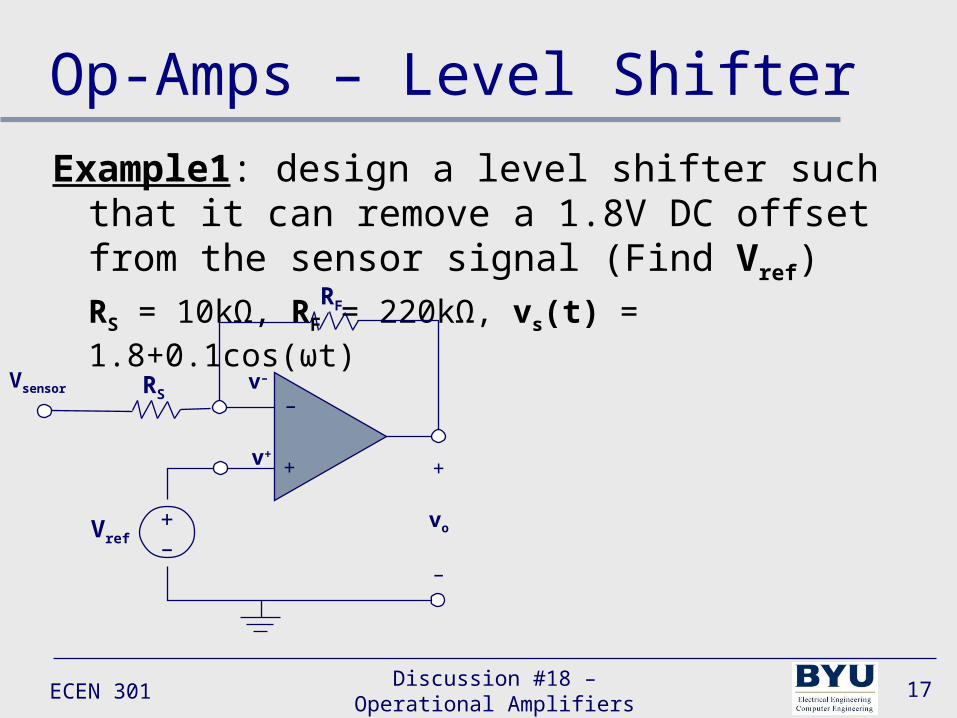
Amplifiers17
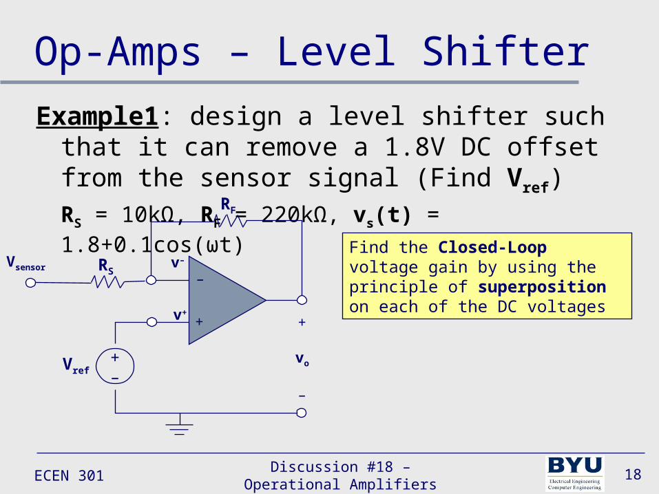
Op-Amps – Level Shifter
Example1: design a level shifter such that it can remove a 1.8V DC offset from the sensor signal (Find Vref)
RS = 10kΩ, RF = 220kΩ, vs(t) = 1.8+0.1cos(ωt)
–
+ +
vo
–
RF
Vref+–
v+
v–RSVsensor
ECEN 301Discussion #18 – Operational
Amplifiers18
Op-Amps – Level Shifter
Example1: design a level shifter such that it can remove a 1.8V DC offset from the sensor signal (Find Vref)
RS = 10kΩ, RF = 220kΩ, vs(t) = 1.8+0.1cos(ωt)
–
+ +
vo
–
RF
Vref+–
v+
v–RSVsensor
Find the Closed-Loop voltage gain by using the principle of superposition on each of the DC voltages
ECEN 301Discussion #18 – Operational
Amplifiers19
Op-Amps – Level Shifter
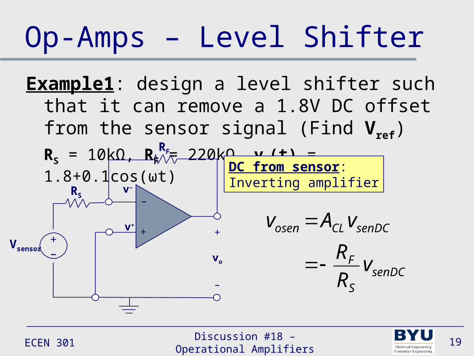
Example1: design a level shifter such that it can remove a 1.8V DC offset from the sensor signal (Find Vref)
RS = 10kΩ, RF = 220kΩ, vs(t) = 1.8+0.1cos(ωt)
–
+ +
vo
–
RF
v+
v–RS
Vsensor+–
DC from sensor:Inverting amplifier
senDCS
F
senDCCLosen
vRR
vAv
ECEN 301Discussion #18 – Operational
Amplifiers20
Op-Amps – Level Shifter
Example1: design a level shifter such that it can remove a 1.8V DC offset from the sensor signal (Find Vref)
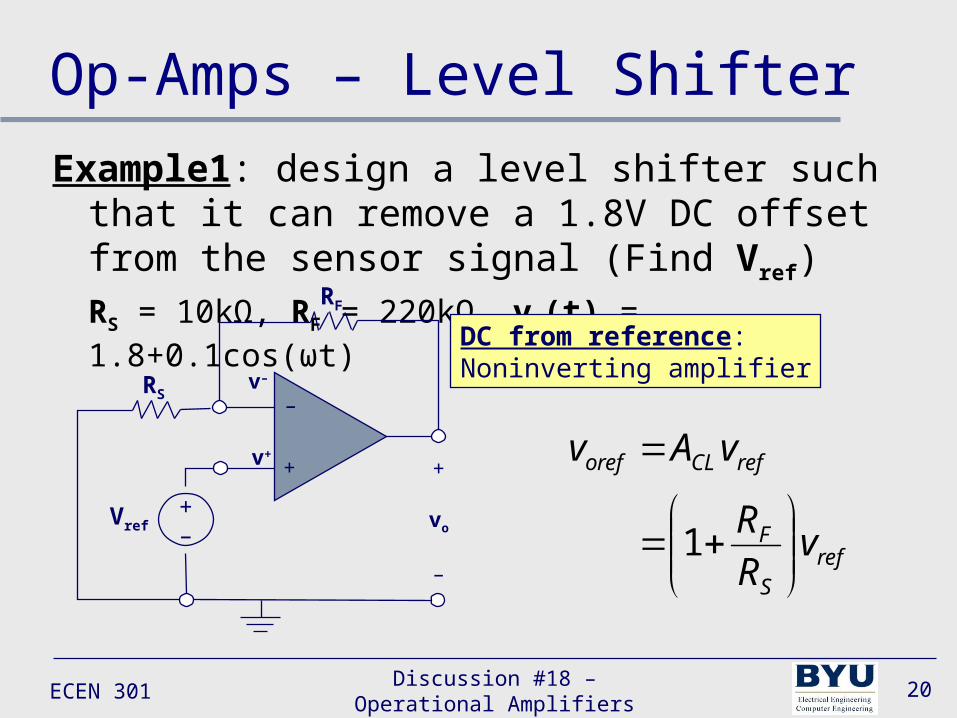
RS = 10kΩ, RF = 220kΩ, vs(t) = 1.8+0.1cos(ωt)
–
+ +
vo
–
RF
v+
v–RS
Vref+–
DC from reference:Noninverting amplifier
refS
F
refCLoref
vRR
vAv
1
ECEN 301Discussion #18 – Operational
Amplifiers21
Op-Amps – Level Shifter
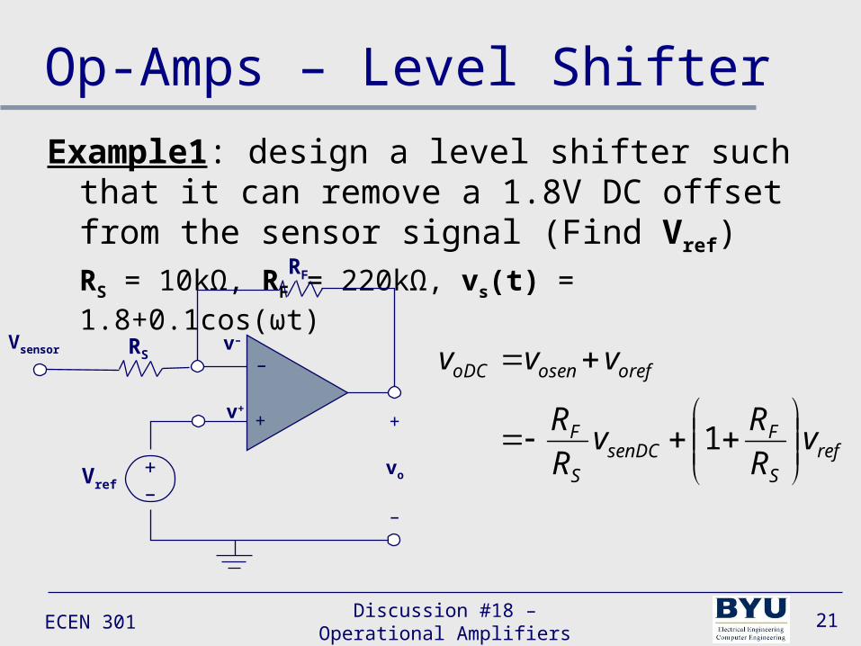
Example1: design a level shifter such that it can remove a 1.8V DC offset from the sensor signal (Find Vref)
RS = 10kΩ, RF = 220kΩ, vs(t) = 1.8+0.1cos(ωt)
refS
FsenDC
S
F
orefosenoDC
vRR
vRR
vvv
1
–
+ +
vo
–
RF
Vref+–
v+
v–RSVsensor
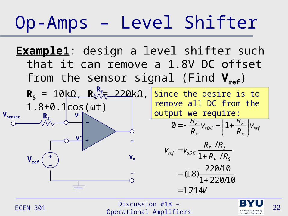
ECEN 301Discussion #18 – Operational
Amplifiers22
Op-Amps – Level Shifter
Example1: design a level shifter such that it can remove a 1.8V DC offset from the sensor signal (Find Vref)
RS = 10kΩ, RF = 220kΩ, vs(t) = 1.8+0.1cos(ωt)
V
RR
RRvv
vRR
vRR
SF
SFsDCref
refS
FsDC
S
F
714.110/2201
10/220)8.1(
/1
/
10
–
+ +
vo
–
RF
Vref+–
v+
v–RSVsensor
Since the desire is to remove all DC from the output we require:
ECEN 301Discussion #18 – Operational
Amplifiers23
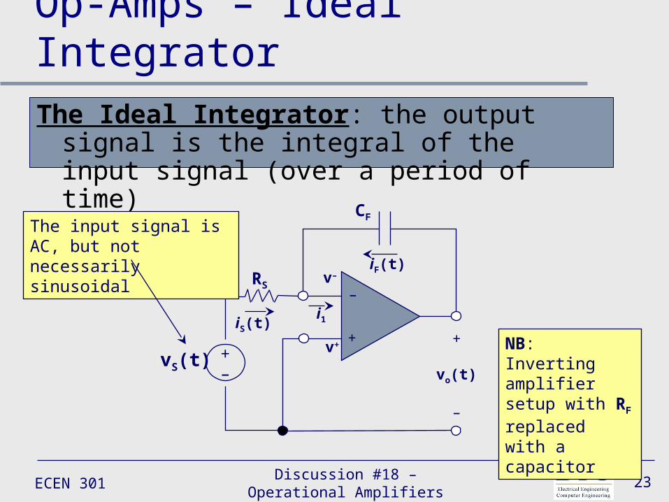
Op-Amps – Ideal Integrator
The Ideal Integrator: the output signal is the integral of the input signal (over a period of time)
–
+ +
vo(t)
–
i1
CF
RS
vS(t)+–
v+
v–iF(t)
iS(t)
The input signal is AC, but not necessarily sinusoidal
NB: Inverting amplifier setup with RF replaced with a capacitor
ECEN 301Discussion #18 – Operational
Amplifiers24
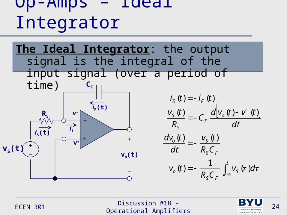
Op-Amps – Ideal Integrator
The Ideal Integrator: the output signal is the integral of the input signal (over a period of time)
–
+ +
vo(t)
–
i1
CF
RS
vS(t)+–
v+
v–iF(t)
iS(t)
t
SFS
o
FS
So
oF
S
S
FS
dvCR
tv
CR
tv
dt
tdv
dt
tvtvdC
R
tv
titi
)(1
)(
)()(
)()()(
)()(
ECEN 301Discussion #18 – Operational
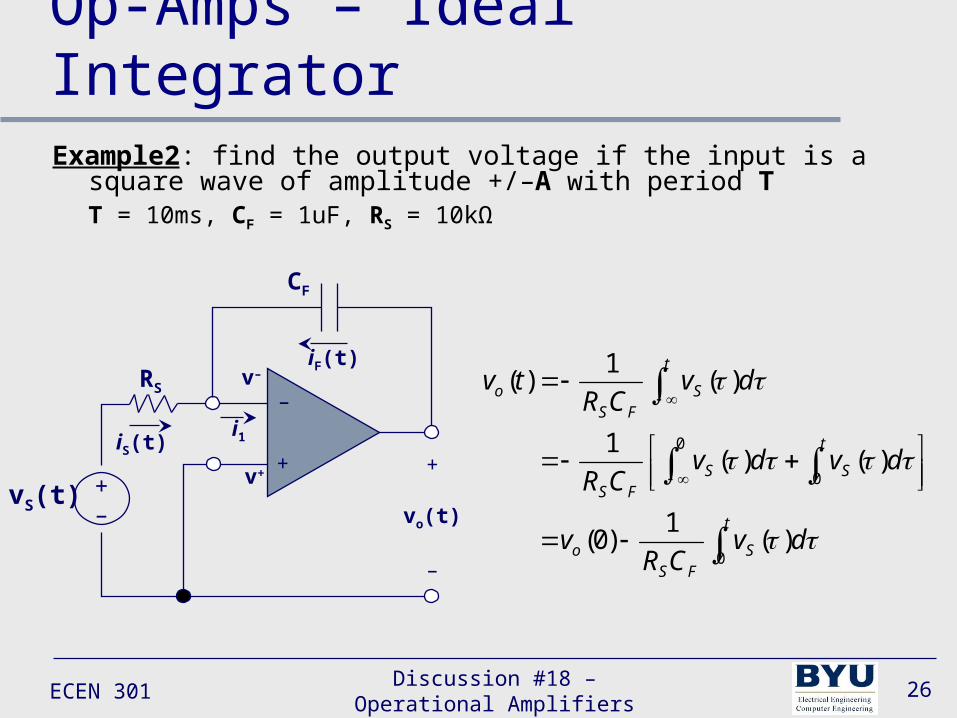
Amplifiers25
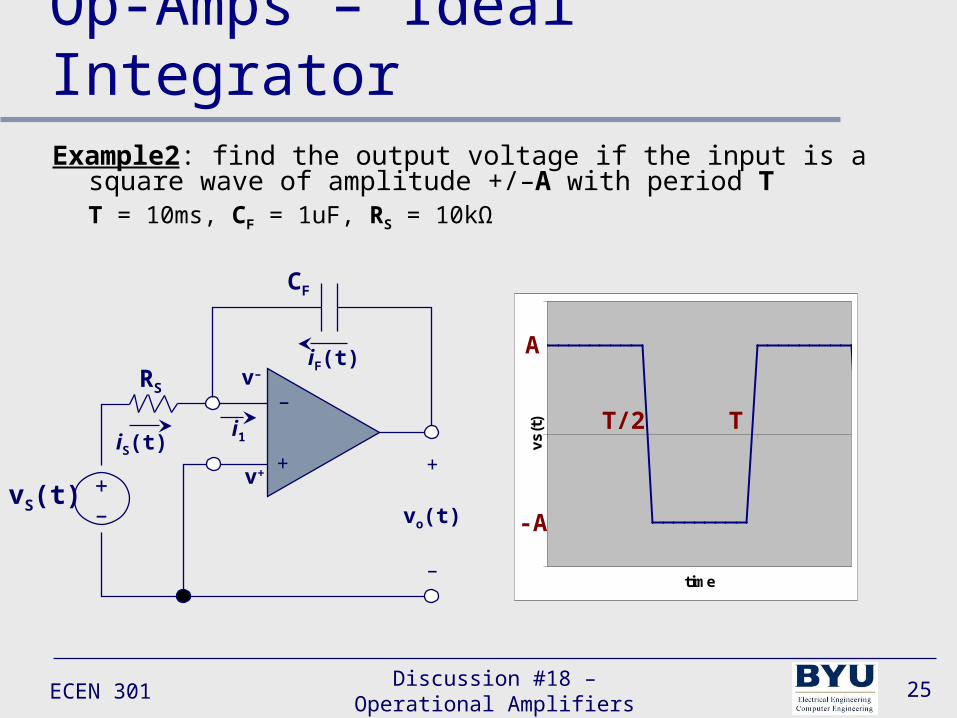
Op-Amps – Ideal IntegratorExample2: find the output voltage if the input is a square wave of amplitude
+/–A with period TT = 10ms, CF = 1uF, RS = 10kΩ
–
+ +
vo(t)
–
i1
CF
RS
vS(t)+–
v+
v–iF(t)
iS(t)
time
vs(t)
A
-A
T/2 T
ECEN 301Discussion #18 – Operational
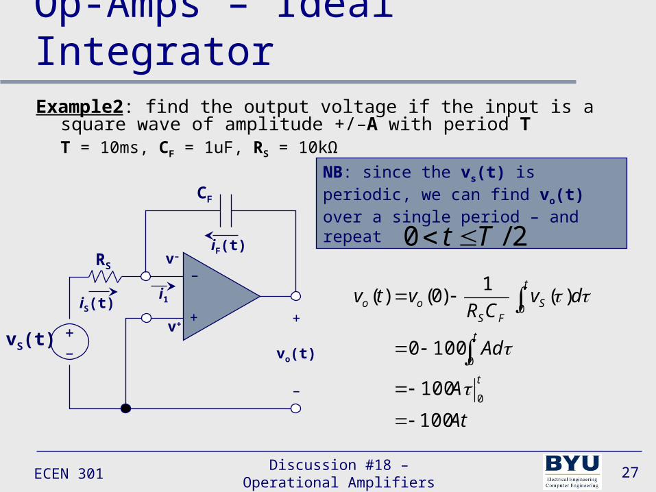
Amplifiers26
Op-Amps – Ideal IntegratorExample2: find the output voltage if the input is a square wave of
amplitude +/–A with period TT = 10ms, CF = 1uF, RS = 10kΩ
–
+ +
vo(t)
–
i1
CF
RS
vS(t)+–
v+
v–iF(t)
iS(t)
t
SFS
o
t
SSFS
t
SFS
o
dvCR
v
dvdvCR
dvCR
tv
0
0
0
)(1
)0(
)()(1
)(1
)(
ECEN 301Discussion #18 – Operational
Amplifiers27
Op-Amps – Ideal IntegratorExample2: find the output voltage if the input is a square wave of
amplitude +/–A with period TT = 10ms, CF = 1uF, RS = 10kΩ
–
+ +
vo(t)
–
i1
CF
RS
vS(t)+–
v+
v–iF(t)
iS(t)
At
A
Ad
dvCR
vtv
t
t
t
SFS
oo
100
100
1000
)(1
)0()(
0
0
0
NB: since the vs(t) is periodic, we can find vo(t) over a single period – and repeat
2/0 Tt
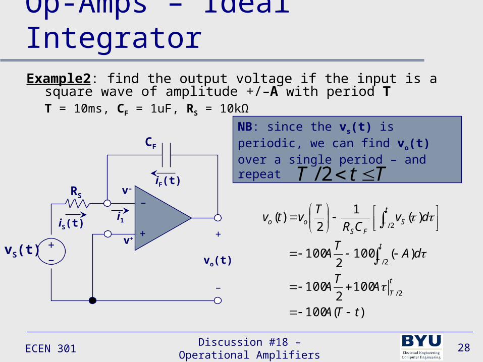
ECEN 301Discussion #18 – Operational
Amplifiers28
Op-Amps – Ideal IntegratorExample2: find the output voltage if the input is a square wave of
amplitude +/–A with period TT = 10ms, CF = 1uF, RS = 10kΩ
–
+ +
vo(t)
–
i1
CF
RS
vS(t)+–
v+
v–iF(t)
iS(t)
)(100
1002
100
)(1002
100
)(1
2)(
2/
2/
2/
tTA
ATA
dATA
dvCR
Tvtv
t
T
t
T
t
T SFS
oo
NB: since the vs(t) is periodic, we can find vo(t) over a single period – and repeat
TtT 2/
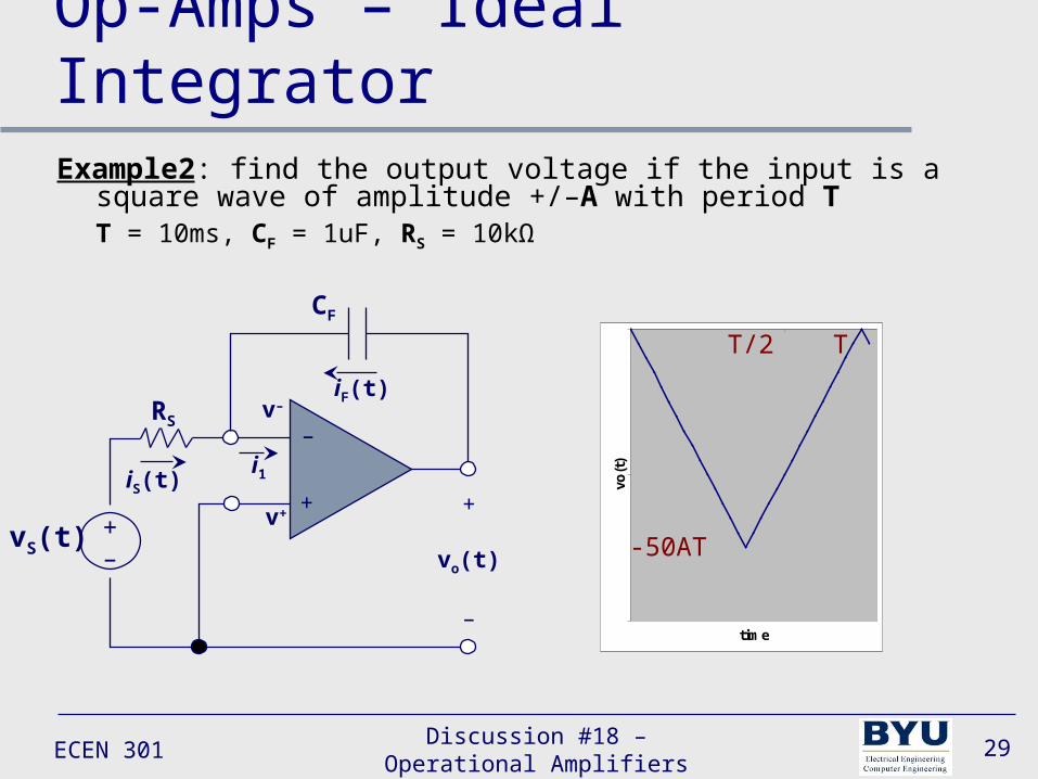
ECEN 301Discussion #18 – Operational
Amplifiers29
Op-Amps – Ideal IntegratorExample2: find the output voltage if the input is a square wave of
amplitude +/–A with period TT = 10ms, CF = 1uF, RS = 10kΩ
–
+ +
vo(t)
–
i1
CF
RS
vS(t)+–
v+
v–iF(t)
iS(t)
timevo(t)
T/2 T
-50AT
ECEN 301Discussion #18 – Operational
Amplifiers30
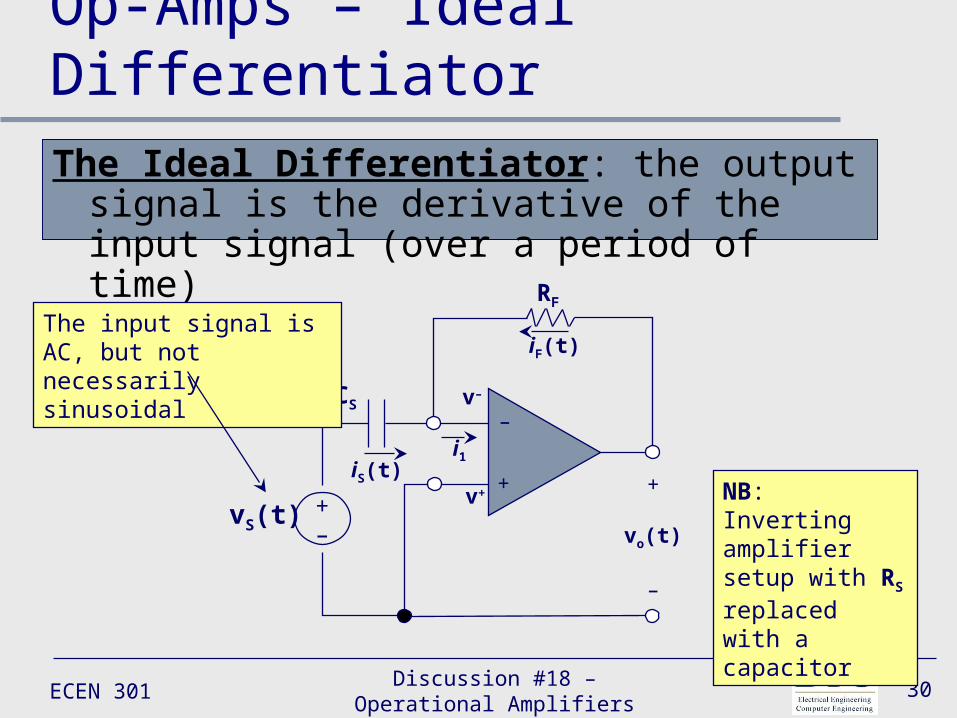
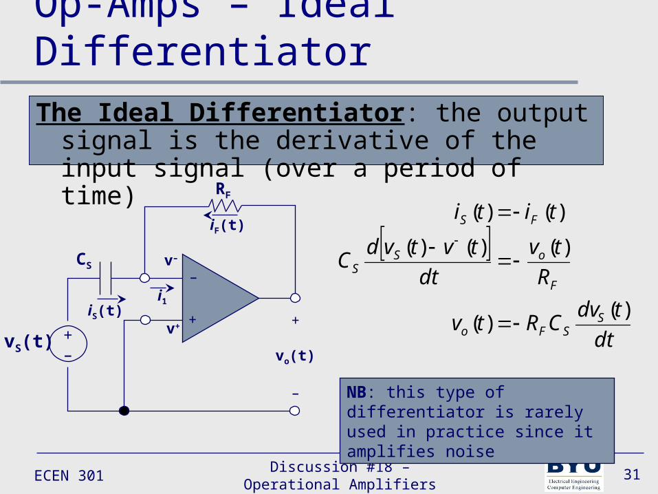
Op-Amps – Ideal Differentiator
The Ideal Differentiator: the output signal is the derivative of the input signal (over a period of time)
–
+ +
vo(t)
–
i1
CS
RF
vS(t)+–
v+
v–
iF(t)
iS(t)
The input signal is AC, but not necessarily sinusoidal
NB: Inverting amplifier setup with RS replaced with a capacitor
ECEN 301Discussion #18 – Operational
Amplifiers31
Op-Amps – Ideal Differentiator
dt
tdvCRtv
R
tv
dt
tvtvdC
titi
SSFo
F
oSS
FS
)()(
)()()(
)()(
NB: this type of differentiator is rarely used in practice since it amplifies noise
The Ideal Differentiator: the output signal is the derivative of the input signal (over a period of time)
–
+ +
vo(t)
–
i1
CS
RF
vS(t)+–
v+
v–
iF(t)
iS(t)
ECEN 301Discussion #18 – Operational
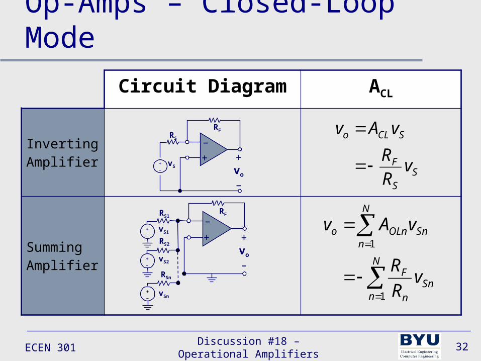
Amplifiers32
Op-Amps – Closed-Loop Mode
Circuit Diagram ACL
Inverting Amplifier
Summing Amplifier
N
nSn
n
F
N
nSnOLno
vR
R
vAv
1
1
–
+ +vo
–
+–
vS
RS
RF
SS
F
SCLo
vRR
vAv
–
+ +vo
–
+–
+–
+–
RSn
RS2
RS1
vSn
vS2
vS1
RF
ECEN 301Discussion #18 – Operational
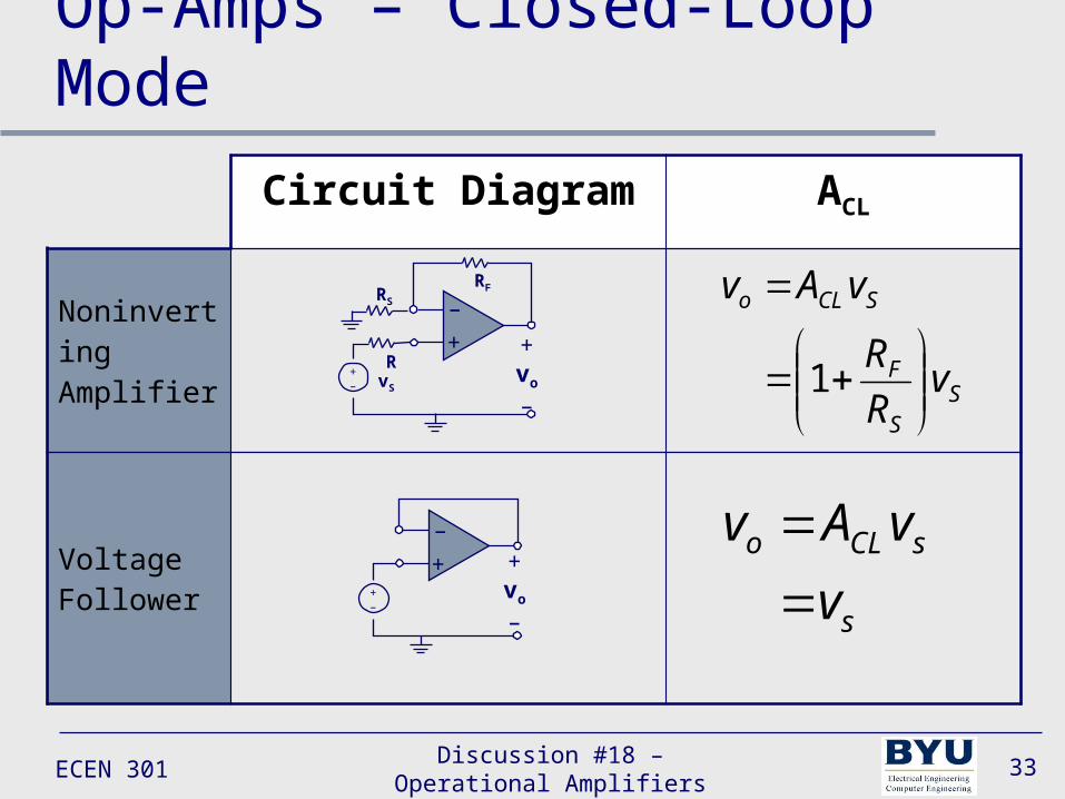
Amplifiers33
Op-Amps – Closed-Loop Mode
Circuit Diagram ACL
Noninverting Amplifier
Voltage Follower
s
sCLo
v
vAv
SS
F
SCLo
vR
R
vAv
1
–
+ +vo
–
+–
R
RS
RF
vS
–
+ +vo
–
+–
ECEN 301Discussion #18 – Operational
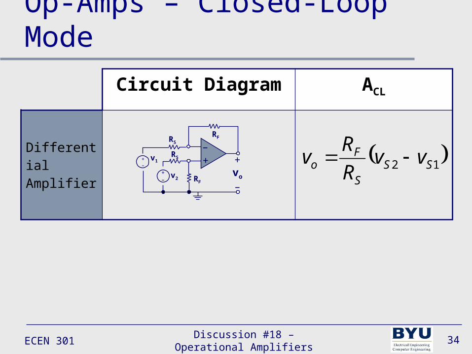
Amplifiers34
Op-Amps – Closed-Loop Mode
Circuit Diagram ACL
Differential Amplifier
12 SSS
Fo vv
R
Rv
–+ +
vo
–
+–
+–
RS
RS
RF
RF
v1
v2
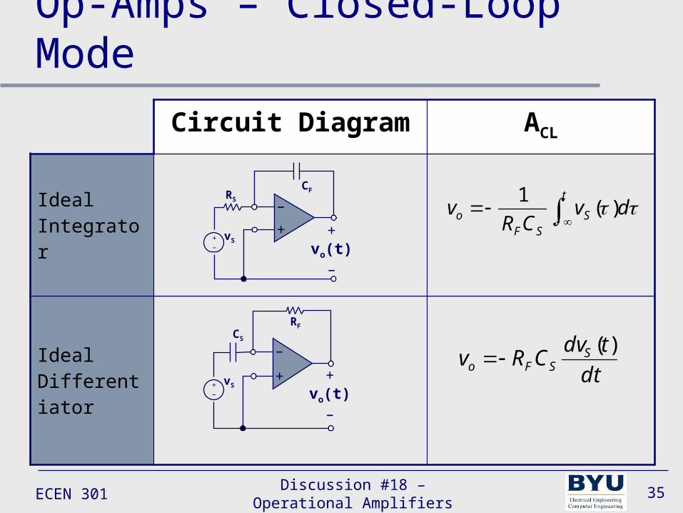
ECEN 301Discussion #18 – Operational
Amplifiers35
Op-Amps – Closed-Loop Mode
Circuit Diagram ACL
Ideal Integrator
Ideal Differentiator
dt
tdvCRv SSFo
)(
t
SSF
o dvCR
v )(1
–
+ +vo(t)
–
+–
vS
CS
RF
–
+ +vo(t)
–
+–
vS
RS
CF
ECEN 301Discussion #18 – Operational
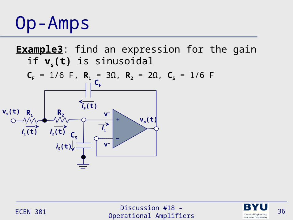
Amplifiers36
Op-Amps Example3: find an expression for the gain if vs(t) is sinusoidal
CF = 1/6 F, R1 = 3Ω, R2 = 2Ω, CS = 1/6 F
+
–
vo(t)i1
CF
R2 v+
v–
iF(t)
i2(t)
R1
i1(t) CS
iS(t)
vs(t)
ECEN 301Discussion #18 – Operational
Amplifiers37
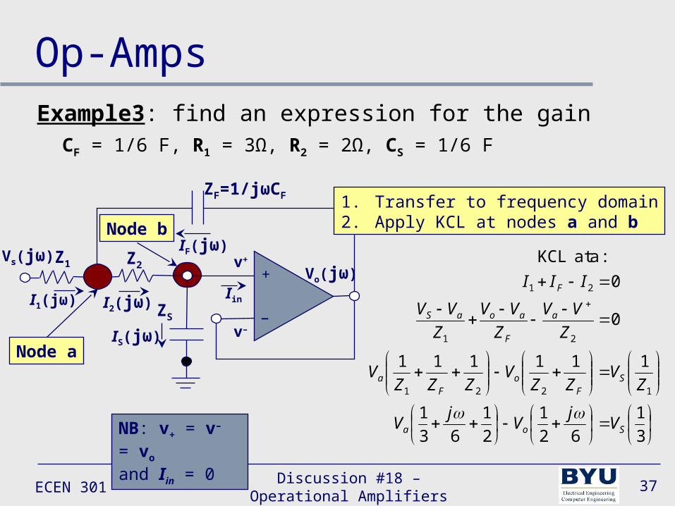
Op-Amps
+
–
Vo(jω)Iin
ZF=1/jωCF
Z2 v+
v–
IF(jω)
I2(jω)
Z1
I1(jω)ZS
IS(jω)
Vs(jω)
Node a
Node b
3
1
62
1
2
1
63
1
111111
0
0
:aat KCL
1221
21
21
Soa
SF
oF
a
a
F
aoaS
F
Vj
Vj
V
ZV
ZZV
ZZZV
Z
VV
Z
VV
Z
VV
III
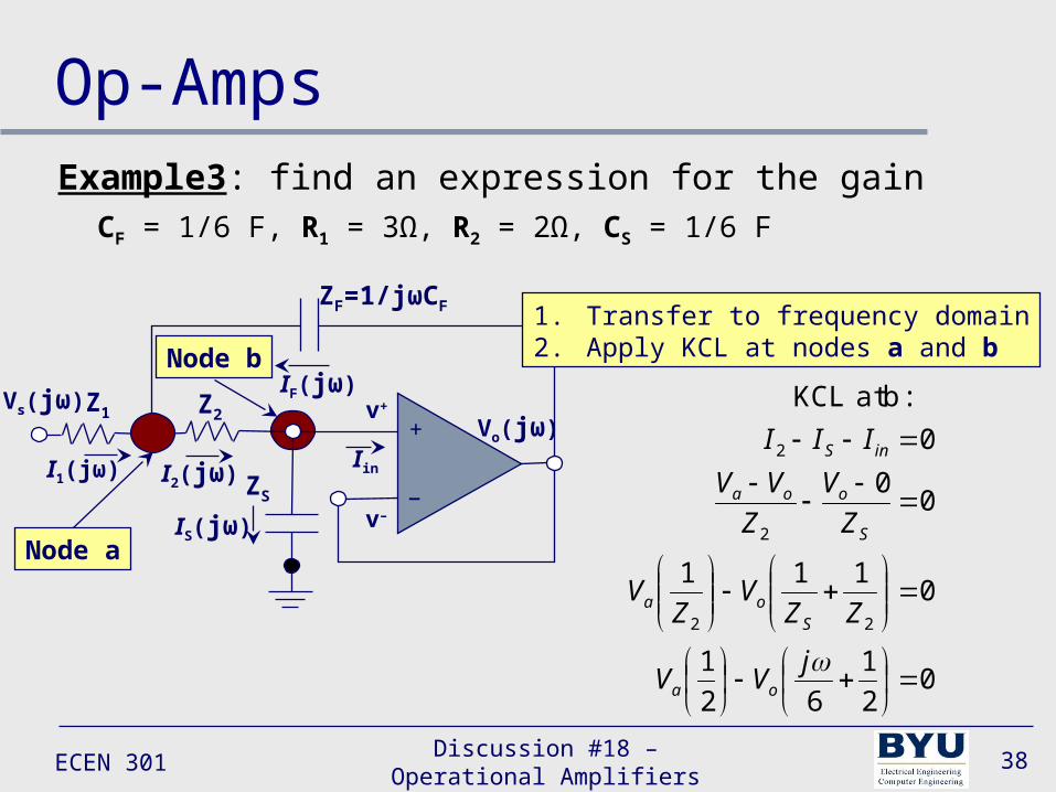
1. Transfer to frequency domain2. Apply KCL at nodes a and b
NB: v+ = v– = vo
and Iin = 0
Example3: find an expression for the gainCF = 1/6 F, R1 = 3Ω, R2 = 2Ω, CS = 1/6 F
ECEN 301Discussion #18 – Operational
Amplifiers38
Op-Amps
+
–
Vo(jω)Iin
ZF=1/jωCF
Z2 v+
v–
IF(jω)
I2(jω)
Z1
I1(jω)ZS
IS(jω)
Vs(jω)
Node a
Node b
02
1
62
1
0111
00
0
:bat KCL
22
2
2
jVV
ZZV
ZV
Z
V
Z
VV
III
oa
Soa
S
ooa
inS
1. Transfer to frequency domain2. Apply KCL at nodes a and b
Example3: find an expression for the gainCF = 1/6 F, R1 = 3Ω, R2 = 2Ω, CS = 1/6 F
ECEN 301Discussion #18 – Operational
Amplifiers39
Op-Amps
033 jVV oa
+
–
Vo(jω)Iin
ZF=1/jωCF
Z2 v+
v–
IF(jω)
I2(jω)
Z1
I1(jω)ZS
IS(jω)
Vs(jω)
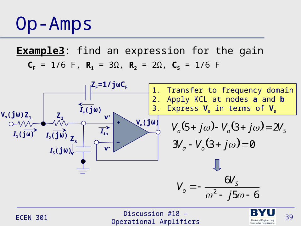
1. Transfer to frequency domain2. Apply KCL at nodes a and b3. Express Vo in terms of Vs
Soa VjVjV 235
65
62
j
VV So
Example3: find an expression for the gainCF = 1/6 F, R1 = 3Ω, R2 = 2Ω, CS = 1/6 F
ECEN 301Discussion #18 – Operational
Amplifiers40
Op-Amps
+
–
Vo(jω)Iin
ZF=1/jωCF
Z2 v+
v–
IF(jω)
I2(jω)
Z1
I1(jω)ZS
IS(jω)
Vs(jω)
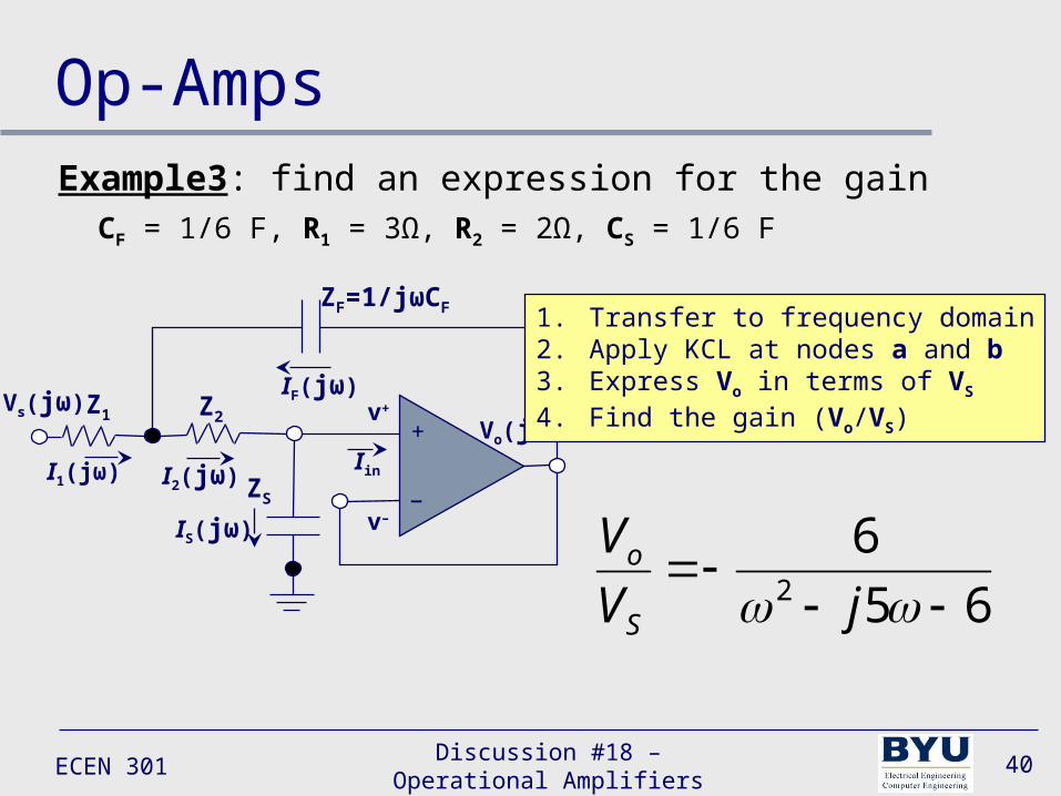
1. Transfer to frequency domain2. Apply KCL at nodes a and b3. Express Vo in terms of VS
4. Find the gain (Vo/VS)
65
62
jV
V
S
o
Example3: find an expression for the gainCF = 1/6 F, R1 = 3Ω, R2 = 2Ω, CS = 1/6 F