ECE 353 Introduction to Microprocessor Systems Michael J. Schulte Week 2.
28
ECE 353 Introduction to Microprocessor Systems Michael J. Schulte Week 2
-
Upload
preston-daniel -
Category
Documents
-
view
220 -
download
0
Transcript of ECE 353 Introduction to Microprocessor Systems Michael J. Schulte Week 2.

ECE 353Introduction to Microprocessor Systems
Michael J. Schulte
Week 2

Tutorial Reminder
Wednesday, February 13th, 2008Keil uVision3 tutorial 6:30-8:00pmEH1249

TopicsMicroprocessor OrganizationOrganization of Microprocessor SystemsEndian-nessARM History and CharacteristicsARM7TDMI ImplementationADuC7026 Overview

Microprocessor ComponentsRegister file Program counter General purpose registers Hidden registers
ALUBusesMemory interface Signal conventions
Control and timing unit

A Simple P Architecture16
ACCUMULATOR
REGISTER PROGRAM COUNTER ADDRESS REGISTERTEMPORARY
TEMP REG GEN REG 0
GEN REG 1
GEN REG 2
GEN REG 3
INST REG
INSTRUCTION DECODERTIMING AND CONTROL
FLAGS
CLOCKGENERATOR
ARITHMETIC AND LOGIC UNIT(ALU)
F
ARPCTR0
IRR0
R1
R2
R3
AInternal Data Bus
ADDR
DATA
/WR
/RD
/RESET
8
A less simple architecture

Instruction Set Architecture (ISA)
Complex Instruction Set (CISC) Single instructions for complex tasks
(string search, block move, FFT, etc.) Usually have variable length instructions Registers have specialized functions
Reduced Instruction Set (RISC) Instructions for simple operations only Usually fixed length instructions Large orthogonal register sets

Register ArchitecturesAccumulator One instruction operand comes from a dedicated
register (the accumulator) closely coupled to the ALU.
Register-Memory Instruction operands can be obtained from both
registers and memory Commonly used in CISC machines
Load-Store All operands must be in general-purpose registers Only a very limited number of instructions
(loads/stores) can “touch” memory Commonly used in RISC machines

Microprocessor System Organization
Memory Architectures Von Neumann architecture Harvard architecture Input/Output (I/O)
Memory-mapped I/O Isolated I/O
Examples
Programmer’s Model aka Register View
Memory Maps

Endian-nessByte Ordering for Little Endian vs. Big Endian
Memory Address
+0 +1 +2 +3
Big Endian Byte 0
Byte 1
Byte 2
Byte 3
MSB in the lowest (first) memory address
Little Endian
Byte 3
Byte 2
Byte 1
Byte 0
LSB in the lowest (first) memory address
Byte 0
Byte 1
Byte 2
Byte 3
Most Significant Byte (MSB)
Least Significant Byte (LSB)

101010
ARM Ltd
Founded in November 1990 Spun out of Acorn Computers
Designs the ARM range of RISC processor cores Licenses ARM core designs to semiconductor
partners who fabricate and sell to their customers. ARM does not fabricate silicon itself
Also develop technologies to assist with the design-in of the ARM architecture Software tools, boards, debug hardware,
application software, bus architectures, peripherals etc

111111
ARM Partnership Model

121212
ARM Powered Products

ARM7 CharacteristicsDesigned to be a simple, efficient RISC core Small die area Low power Low interrupt latency
These characteristics enabled ARM to become dominant in the cell phone market. Most cell phones contain a heterogenous
multiprocessor SoC with an ARM and a DSP.
Advanced ARM designs (ARM9,10,11) have become much more sophisticated (i.e. Intel Xscale in PDAs), but have had less success in penetrating other markets where power consumption issues are not as severe.

ARM7TDMI Implementation
The ARM7TDMI uses the ARM v4T ISA. All instructions are conditional
The ARM7TDMI is a basic load-store RISC Sixteen GP registers (R15-R0) with banking Three stage pipeline (FDE) No caches Support for ARM (32-bit) and Thumb (16-
bit) instruction sets Multiply-accumulate (MAC) unit On-chip hardware debug support
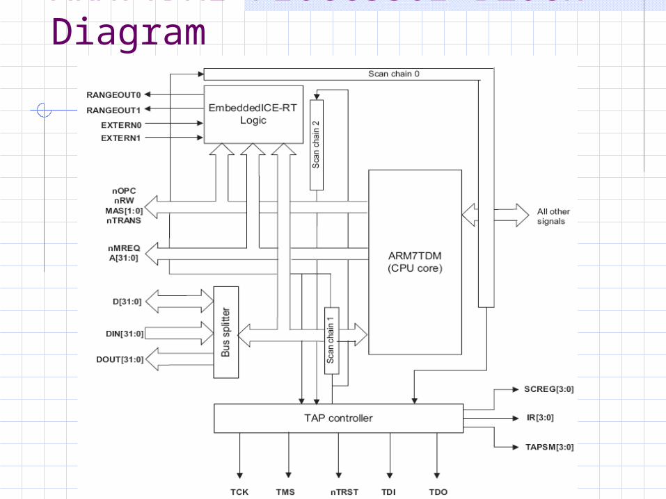
ARM7TDMI Processor Block Diagram
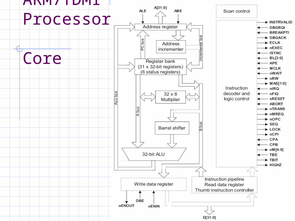
ARM7TDMIProcessor Core

Analog Devices ADuC7026ARM7TDMI core 62kB flash, 8kB SRAM In-circuit programmable, JTAG debug 41.78MHz PLL with programmable divider Little-endian
Numerous digital peripherals GPIO Timers (GP x4 and watchdog/wake-up) UART/I2C/SPI serial interfaces 3-phase PWM External memory interface (16-bit multiplexed)
Analog input/output 12 in, 4 out Voltage reference and temperature sensor

ADuC7026 Block Diagram

ADuC7026 Memory Map

ADuC7026 Pin-Out (LQFP-80)

AssessmentTeam ConcepTestIn-Class Address Decoding Exercise

Wrapping UpWeek 3 reading is chapters 5, 6.1-6.11, 6.14 from the textbook, the ARM7TDMI Technical Reference Manual chapter 2, and Supplement #1 (LearnContent)Pre-Quiz #2 to be done by Tuesday 2/5 at midnightHomework #1 due Wednesday 2/6Tutorial on Wednesday 2/13 from 6:30-8:00pm in EH1249
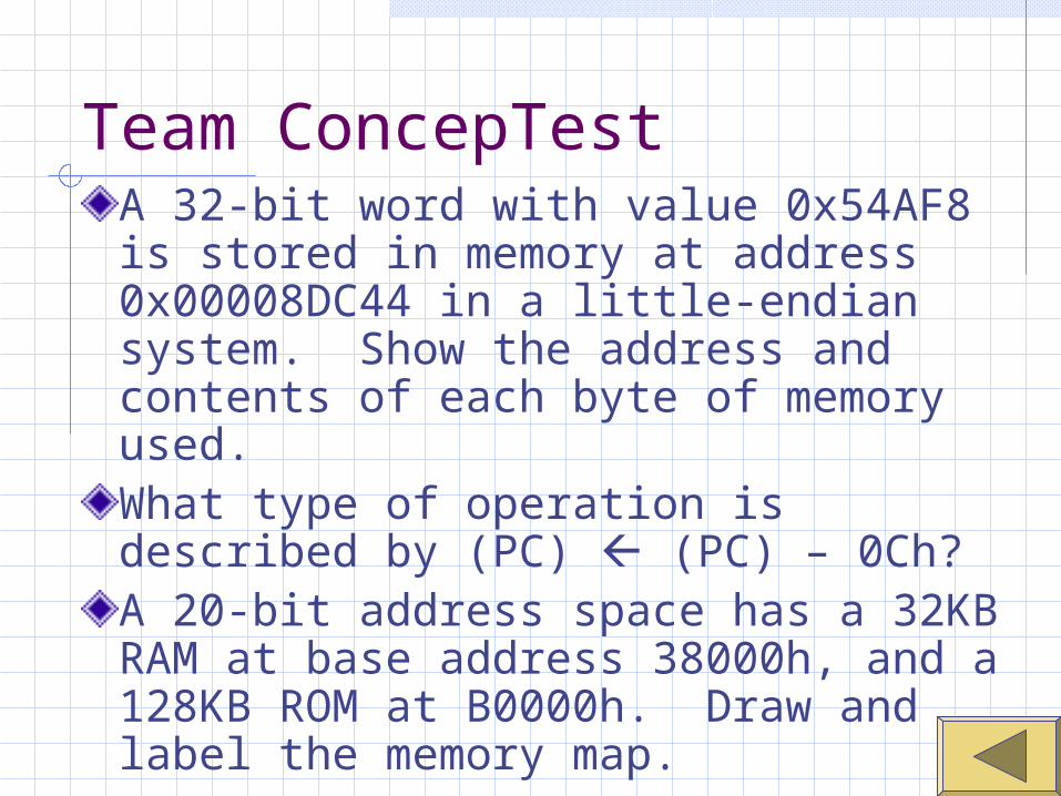
Team ConcepTestA 32-bit word with value 0x54AF8 is stored in memory at address 0x00008DC44 in a little-endian system. Show the address and contents of each byte of memory used.What type of operation is described by (PC) (PC) – 0Ch?A 20-bit address space has a 32KB RAM at base address 38000h, and a 128KB ROM at B0000h. Draw and label the memory map.

In-Class ExerciseDesign decode logic for the following devices with the indicated control inputs: 64Kx8 ROM (/CS, /OE) at 0x04XXXX 1Mx8 RAM (/CS, /OE, /WE) at 0xA00000 Input Port (/OE) at 0xFXXX00 Output Port (/WR) at 0x1XXXXX
In all cases, assume a 24-bit address bus (A23:0) and control signals (/RD, /WR)

TMS320C671XOrganization

Register View of a Simple P
ACC
FLAGS
R0
R1
R2
Registers
R3
Memory
0000h
FFFFh
aka “Von Neumann” or “Princeton” architecture
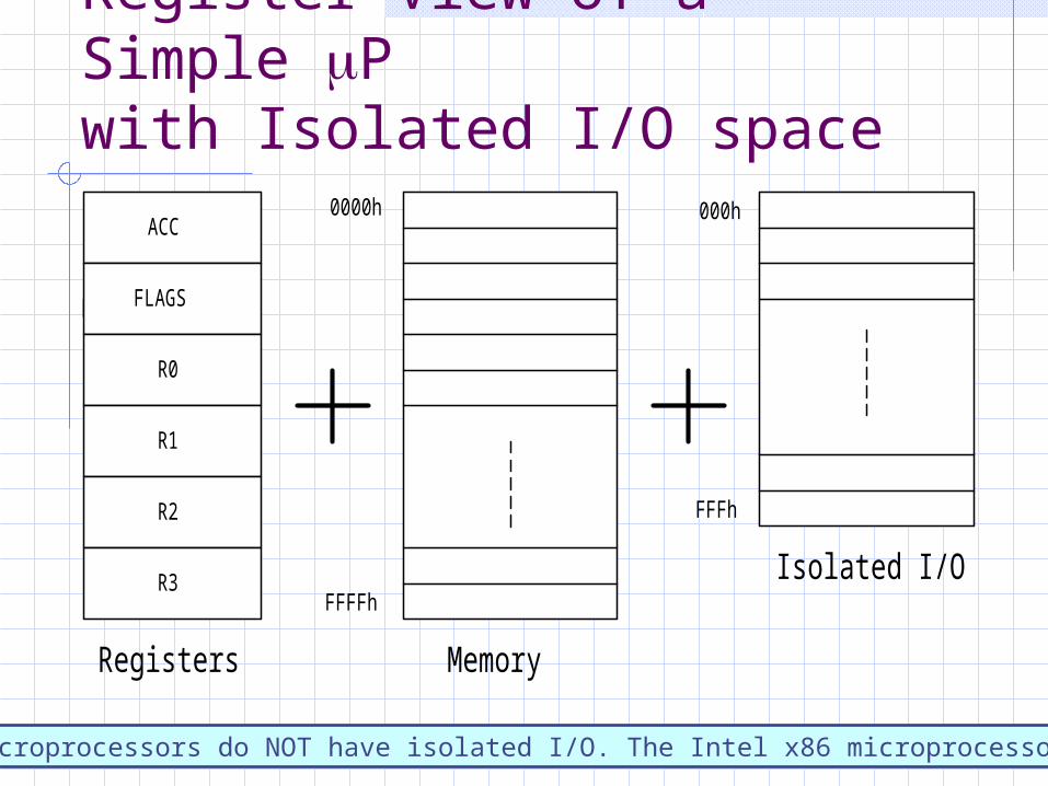
Register View of a Simple Pwith Isolated I/O space
ACC
FLAGS
R0
R1
R2
Registers
R3
Memory
Isolated I/O
0000h
FFFFh
000h
FFFh
Most microprocessors do NOT have isolated I/O. The Intel x86 microprocessors do.

Register View of a Simple P with Separate Code and Data Memories
ACC
FLAGS
R0
R1
R2
Registers
R3
Program
Data
0000h
FFFFh
000h
7FFh
Isolated I/O
000h
FFFh
Memory(optional)
aka “Harvard” architecture