Durable diamond-like carbon templates for UV nanoimprint ...
7
IOP PUBLISHING NANOTECHNOLOGY Nanotechnology 19 (2008) 105302 (7pp) doi:10.1088/0957-4484/19/10/105302 Durable diamond-like carbon templates for UV nanoimprint lithography L Tao 1 , S Ramachandran 1 , C T Nelson 1 , M Lin 2 , L J Overzet 1 , M Goeckner 1 , G Lee 1 , C G Willson 2 , W Wu 3 and W Hu 1,4 1 Department of Electrical Engineering, University of Texas at Dallas, Richardson, TX 75083, USA 2 Department of Chemical Engineering, University of Texas at Austin, Austin, TX 78712, USA 3 Quantum Science Research, HP Labs, Hewlett-Packard Company, Palo Alto, CA 94304, USA E-mail: [email protected] Received 26 October 2007, in final form 7 January 2008 Published 13 February 2008 Online at stacks.iop.org/Nano/19/105302 Abstract The interaction between resist and template during the separation process after nanoimprint lithography (NIL) can cause the formation of defects and damage to the templates and resist patterns. To alleviate these problems, fluorinated self-assembled monolayers (F-SAMs, i.e. tridecafluoro-1,1,2,2,tetrahydrooctyl trichlorosilane or FDTS) have been employed as template release coatings. However, we find that the FDTS coating undergoes irreversible degradation after only 10 cycles of UV nanoimprint processes with SU-8 resist. The degradation includes a 28% reduction in surface F atoms and significant increases in the surface roughness. In this paper, diamond-like carbon (DLC) films were investigated as an alternative material not only for coating but also for direct fabrication of nanoimprint templates. DLC films deposited on quartz templates in a plasma enhanced chemical vapor deposition system are shown to have better chemical and physical stability than FDTS. After the same 10 cycles of UV nanoimprints, the surface composition as well as the roughness of DLC films were found to be unchanged. The adhesion energy between the DLC surface and SU-8 is found to be smaller than that of FDTS despite the slightly higher total surface energy of DLC. DLC templates with 40 nm features were fabricated using e-beam lithography followed by Cr lift-off and reactive ion etching. UV nanoimprinting using the directly patterned DLC templates in SU-8 resist demonstrates good pattern transfer fidelity and easy template–resist separation. These results indicate that DLC is a promising material for fabricating durable templates for UV nanoimprint lithography. (Some figures in this article are in colour only in the electronic version) 1. Introduction Nanoimprint lithography (NIL), especially the ultraviolet (UV) version, has been considered by the semiconductor industry as one of the candidates for next generation manufacturing technology because of its high patterning resolution and low cost compared to state-of-the-art photolithography [1]. In UV-NIL, UV exposure is used to cure imprinted resist patterns in a template, allowing fast and room-temperature 4 Author to whom any correspondence should be addressed. processing without pattern distortion. In order to achieve high throughput, the scheme of step and flash imprint lithography (S-FIL), a scanner-like UV-NIL, is most promising [2]. Sequential step and imprint on large wafers will require precise alignment, durable and anti-sticky template surfaces, low defect density, and excellent pattern reproducibility. Due to the ‘contact printing’ nature of NIL, most of these issues are strongly related to the template–resist adhesion [3–5]. Currently, fluorinated self-assembled monolayers (F-SAMS), such as tridecafluoro-1,1,2,2,tetrahydrooctyl trichlorosilane (FDTS; Gelest) [3], are widely used to coat the templates, 0957-4484/08/105302+07$30.00 © 2008 IOP Publishing Ltd Printed in the UK 1
Transcript of Durable diamond-like carbon templates for UV nanoimprint ...

IOP PUBLISHING NANOTECHNOLOGY
Nanotechnology 19 (2008) 105302 (7pp) doi:10.1088/0957-4484/19/10/105302
Durable diamond-like carbon templatesfor UV nanoimprint lithographyL Tao1, S Ramachandran1, C T Nelson1, M Lin2, L J Overzet1,M Goeckner1, G Lee1, C G Willson2, W Wu3 and W Hu1,4
1 Department of Electrical Engineering, University of Texas at Dallas, Richardson,TX 75083, USA2 Department of Chemical Engineering, University of Texas at Austin, Austin,TX 78712, USA3 Quantum Science Research, HP Labs, Hewlett-Packard Company, Palo Alto,CA 94304, USA
E-mail: [email protected]
Received 26 October 2007, in final form 7 January 2008Published 13 February 2008Online at stacks.iop.org/Nano/19/105302
AbstractThe interaction between resist and template during the separation process after nanoimprintlithography (NIL) can cause the formation of defects and damage to the templates and resistpatterns. To alleviate these problems, fluorinated self-assembled monolayers (F-SAMs,i.e. tridecafluoro-1,1,2,2,tetrahydrooctyl trichlorosilane or FDTS) have been employed astemplate release coatings. However, we find that the FDTS coating undergoes irreversibledegradation after only 10 cycles of UV nanoimprint processes with SU-8 resist. Thedegradation includes a 28% reduction in surface F atoms and significant increases in the surfaceroughness. In this paper, diamond-like carbon (DLC) films were investigated as an alternativematerial not only for coating but also for direct fabrication of nanoimprint templates. DLC filmsdeposited on quartz templates in a plasma enhanced chemical vapor deposition system areshown to have better chemical and physical stability than FDTS. After the same 10 cycles ofUV nanoimprints, the surface composition as well as the roughness of DLC films were found tobe unchanged. The adhesion energy between the DLC surface and SU-8 is found to be smallerthan that of FDTS despite the slightly higher total surface energy of DLC. DLC templates with40 nm features were fabricated using e-beam lithography followed by Cr lift-off and reactiveion etching. UV nanoimprinting using the directly patterned DLC templates in SU-8 resistdemonstrates good pattern transfer fidelity and easy template–resist separation. These resultsindicate that DLC is a promising material for fabricating durable templates for UV nanoimprintlithography.
(Some figures in this article are in colour only in the electronic version)
1. Introduction
Nanoimprint lithography (NIL), especially the ultraviolet (UV)version, has been considered by the semiconductor industryas one of the candidates for next generation manufacturingtechnology because of its high patterning resolution andlow cost compared to state-of-the-art photolithography [1].In UV-NIL, UV exposure is used to cure imprinted resistpatterns in a template, allowing fast and room-temperature
4 Author to whom any correspondence should be addressed.
processing without pattern distortion. In order to achieve highthroughput, the scheme of step and flash imprint lithography(S-FIL), a scanner-like UV-NIL, is most promising [2].Sequential step and imprint on large wafers will requireprecise alignment, durable and anti-sticky template surfaces,low defect density, and excellent pattern reproducibility. Dueto the ‘contact printing’ nature of NIL, most of these issuesare strongly related to the template–resist adhesion [3–5].Currently, fluorinated self-assembled monolayers (F-SAMS),such as tridecafluoro-1,1,2,2,tetrahydrooctyl trichlorosilane(FDTS; Gelest) [3], are widely used to coat the templates,
0957-4484/08/105302+07$30.00 © 2008 IOP Publishing Ltd Printed in the UK1

Nanotechnology 19 (2008) 105302 L Tao et al
resulting in super-hydrophobic surfaces to prevent resiststicking. However, F-SAMS gradually lose F atoms to the airand were recently found to chemically react irreversibly withUV-curable resists [6, 7]. This causes defects and even damageto the template, resulting in poor pattern reproducibility. Thedevelopment of NIL templates with both chemical and physicalstability is a necessity if UV-NIL is to meet the requirementsfor mass production of semiconductor and nanotech products.
In this study, the stability of F-SAMS coatings is furtherevaluated. Significant degradation of the F-SAMS coatingsis observed after only 10 imprint cycles. Previously, wehave developed diamond-like carbon (DLC) as an alternativetemplate material with improved scratch and wear resistancefor thermal NIL [8]. Here, we study the durability of the DLCtemplate for UV nanoimprinting in comparison to the F-SAMScoating. The interfacial interaction of these coating layerswith UV-curable SU-8 photo resist (Microchem) is investigatedusing surface characterization techniques. The experimentalresults of surface elemental composition, surface roughness,and surface energy indicate that the DLC coating offers muchbetter chemical and physical durability than F-SAMs for UV-NIL. Nanostructures are then fabricated into the DLC filmsusing e-beam lithography (EBL), metal lift-off, and reactiveion etching. Patterned DLC templates are then used in the UVimprint process to produce SU-8 nanoscale structures, whichshow high pattern transfer fidelity and easy release of thetemplate from the resist. DLC is an ideal template material fornanoimprint templates because of its chemical inertness, lowsurface energy, UV transparency, and high hardness.
2. Experiments
2.1. DLC deposition and sample preparation
Si and quartz pieces were cleaned using acetone and thenisopropyl alcohol in an ultrasonic agitation bath for 10 min.After blow-drying in N2, the samples were baked at 100 ◦Con a hot-plate for 2 min, and 20–100 nm thick DLC filmswere grown on the quartz samples using plasma enhancedchemical vapor deposition (PECVD). A mixture of methane(CH4) and argon in the ratio of 3:1 was used as the precursor.An inductively coupled plasma (ICP) system was used todeposit the DLC films in this work. This ICP system is moreversatile than the capacitive coupled plasma (CCP) systemused in our previous work [8]. It allowed us to sustaineither a capacitive plasma (similar to our previous work) oran inductive plasma with or without capacitive power appliedto the chuck. This latter allows the ion bombardment energyat the substrate surface to be controlled independently fromthe plasma creation and ion flux. Such independent controlof ion density and flux to the surface (by ICP coil power) andion bombardment energy (by ‘wafer-chuck’ or ‘bias’ power)enables a wider process test window through increased processcontrol. Even so, one constraint in using the inductive plasmawas ensuring low substrate surface temperatures and so we hadto employ an intermittent plasma with an ON time of 15 s andOFF time of 30 s to obtain good films. We found that the DLCdeposition rate is between 18 and 45 nm min−1 for varying
bias powers of 10 W (−100 V self-bias) to 150 W (−590 Vself-bias) and ICP coil powers (0–200 W). The DLC structureproperties were characterized using Raman spectroscopy (notshown), indicating a sp3/sp2 ratio of around 3:1 to 4:1 withhydrogen content of about 20–30%. We have prepared a set of34 samples, 13 of which were deposited under CCP conditions(ICP coil power = 0) and 21 under ICP conditions (ICP coilpower = 200 W). From the set of these films, we chose twowith the best combination of UV transparency, surface energy,and hardness for imprint testing. These films were depositedunder the following conditions: (a) ICP power = 0 W andbias power = 150 W (self-bias of −590 V) and (b) ICPpower = 200 W and bias power = 10 W (self-bias of −100 V).A systematic study of the effects of the deposition conditionson film properties will be performed in a future work. Inorder to evaluate the imprint performance of DLC films incomparison to F-SAMS, quartz templates with FDTS coatingwere also prepared by immersing the quartz templates in FDTSsolution in n-heptane for 5 min, followed by soaking in acetonefor 2 min, N2 blow dry, and baking on the hot-plate at 100 ◦Cfor 5 min. Both films were stored in the N2 box before andafter experiments.
2.2. UV-NIL
300 nm thick SU-8 (Tg ∼ 55 ◦C) was spin-coated onto Sisamples followed by baking on a hot-plate at 65 ◦C for 1 min,95 ◦C for 2 min, and 65 ◦C for 1 min. UV-NIL processeswere carried out on an Obducat 2.5 nanoimprinter at a pressureof 1.5–6 MPa and a temperature of 25–75 ◦C. A UV lightsource with a broad spectrum output (250–450 nm) and apower of 40–100 mJ cm−2 at the sample was used to exposethe SU-8 resist for 3 s. FDTS and DLC coated quartz sampleswere used as blank templates and 10 UV-NILs were carriedout continuously without cleaning the templates at the sameimprinting conditions. UV-NIL using patterned DLC templateswere also performed on SU-8 coated samples under similarimprint conditions.
2.3. Surface characterization
Surface properties of the FDTS and DLC films before andafter the 10 UV-NIL cycles were characterized using x-rayphotoelectron spectroscopy (XPS). XPS data were collectedusing a PHI 5701 LSci instrument with a monochrome Al Kα
(1486.6 eV) source and an analysis area of about 2.0 mm ×0.8 mm. Because the quartz samples are not conductive,charge correction was carried on correspondingly for FDTSand DLC samples. Contact angles of water and ethylene glycolon the FDTS and DLC films were measured using a RameHart goniometer. Their surface energies were then calculatedusing a two-liquid method [9]. The optical transmission of thesamples was measured using an n&k analyzer 1200RT/Iris 200.The surface roughness of the samples was investigated using aVeeco atomic force microscope (AFM). On each sample, rootmean square (RMS) roughness was obtained by averaging over5 μm2 areas at three different locations.
2

Nanotechnology 19 (2008) 105302 L Tao et al
Figure 1. The transmission spectra of 20–45 nm DLC films on1/4 in thick quartz S-FIL templates. The 20 nm film was deposited atzero coil power, 150 W bias power, and a gas pressure of 50 mTorr.The 45 nm film was deposited at zero coil power, 150 W bias power,and a gas pressure of 40 mTorr. The 35 nm film was deposited at200 W ICP coil power, 10 W bias power, and a gas pressure of40 mTorr. The optical absorbance of the films at the 365 nmwavelength were 11.0, 9.9, and 8.7 (×104 cm−1) for the 20, 45, and35 nm films, respectively.
2.4. Fabrication of the DLC template
The DLC template was fabricated using EBL, metal lift-off, and then a reactive ion etching process. Nanoscalegratings of 40 nm width and spacing were formed in apolymethylmethacrylate (PMMA) resist on the DLC coatedquartz samples using EBL. Typical EBL processes used a beamenergy of 30 keV, an aperture of 15 μm, a beam current of200 pA, a working distance of 5 mm, and cold developmentin methyl isobutyl ketone:isopropyl alcohol (1:3) with 1.5%methyl ethyl ketone [10]. After the development of PMMApatterns, 10 nm thick Cr was evaporated on the sample anda lift-off process was performed in acetone in an ultrasonicbath for 5 min to transfer the PMMA patterns to the Cr layer.Using the Cr gratings as a mask, reactive ion etching usingpure CF4 was performed in a home-made ICP system with anICP power of 400 W, DC bias of 100 V, CF4 35 sccm, and15 mTorr, as discussed in previous work [8]. After the Crresidue was stripped away, patterned DLC nanostructures wereevaluated using AFM and then used as a template in the UV-NIL processes.
3. Results and discussion
3.1. UV transmittance
In the S-FIL or UV-NIL process, UV light with wavelengtharound 365 nm is transmitted through the template to curethe photoresist underneath. The template transmittance atthis wavelength is important for the throughput and powerefficiency of the process. Figure 1 shows the transmissionspectra of the S-FIL templates coated with 20–45 nmthick DLC deposited using different PECVD conditions incomparison to a bare quartz template. The 20 nm DLC coatedquartz template provides close to 70% transmittance aroundthe 365 nm wavelength of interest. The 20 and 45 nm thick
DLC films in figure 1 were deposited using only CCP (ICPpower = 0 W, bias power = 150 W, and self-bias of −590 V)for different lengths of time. The 35 nm film was depositedusing ICP (ICP power = 200 W, bias power = 10 W, andself-bias of −100 V). As shown in figure 1, the films depositedusing CCP and ICP show different absorbance characteristicsin the UV range. The ICP deposited DLC film has a somewhathigher C–H concentration and therefore higher absorbance atshorter wavelengths (e.g. around 200 nm) but lower absorbanceat longer wavelengths (e.g. 365 nm), compared to the 20 nmand 45 nm samples deposited with zero ICP power. For the365 nm UV light of interest, the optical absorption (α) of the35 nm DLC is the lowest (8.7 × 104 cm−1), offering the besttransparency, in comparison to the 20 nm (α ∼ 11×104 cm−1)and 45 nm samples (α ∼ 9.9×104 cm−1). It was also observedthat a lower plasma pressure results in better transparency forthe same deposition power. In addition, increasing the coilpower further at a constant bias power appeared to increase thepolymerization of the precursor and lead to softer films witha higher hydrogen content. Further, increasing the bias power(holding the ICP coil power constant) appeared to increase thesp2 fraction in the film leading to more graphitic films thathave reduced hardness and transmittance. The window forfilms with good properties was found to be 200 ± 100 W forthe ICP coil power and −100 ± 50 V for the DC self-bias atthe particular flow and pressure (40 mTorr) conditions that weemployed.
We understand that the optical transmittance of DLC filmscan be further enhanced by maintaining a narrow ion energydistribution around 100–150 eV, resulting in a high contentof sp3 C–C bonding due to the surface kinetics of the carbondeposition [11]. A lower chamber pressure (e.g. 10 mTorr)and a precursor with lower hydrogen content (e.g. C2H2)can be used, which will be explored in future work. Thehigh transmittance of thick DLC films is promising sincenanostructures can be directly fabricated in the DLC filmsinstead of coating DLC on the patterned quartz templates, forwhich uniform step coverage is quite difficult. The patterningof DLC films is discussed in section 3.4. The presentedPECVD process was chosen for the desired DLC propertiesand has relatively poor step coverage. It may be that theconditions can be optimized to improve step coverage ifneeded.
3.2. Characterization of surface chemistry
XPS elemental concentrations for both FDTS and DLCsurfaces before and after the 10 cycles of UV-NILs are shownin table 1. Samples denoted as ‘FDTS0’ and ‘FDTS10’ referto FDTS coated quartz templates with zero and 10 UV-NILimprint cycles, respectively. Similarly, 100 nm DLC coatedquartz templates are denoted as ‘DLC0’ and ‘DLC10’. Inaddition, figure 2 shows the XPS spectra of the FDTS0 andFDTS10 samples. From table 1, the most noticeable changein the atomic composition is a reduction of the F atom by∼28% after the UV-NIL. There are pronounced changes on thepeak and areas of C–C, CH2–CF2, CF3, and CF2 in the spectraof the FDTS10 sample (figure 2(b)) compared to FDTS0
3

Nanotechnology 19 (2008) 105302 L Tao et al
Figure 2. XPS spectra of the FDTS coated quartz surface (a) before and (b) after 10 cycles of UV nanoimprints.
Table 1. Atomic concentrations (at.%) (Normalized to 100% of theelements detected. XPS does not detect H or He.) of the templatesurfaces before and after 10 cycles of UV-NIL.
Element concentration (%)a
Sample C N O F Si
FDTS0 17.0 0.1 28.5 37.9 16.5FDTS10 17.5 0.3 35.5 27.4 19.3DLC0 85.7 1.3 12.9 0.0 0.0DLC10 83.7 1.0 14.6 0.1 0.6
a The precision of the quantitative data is3–5% for the elements present atconcentrations >10 at.%.
(figure 2(a)). To quantify these changes, the decomposition ofthe carbon 1s spectral curves for the FDTS samples is shownin table 2 with the integrated area (%) for each component.The area% at 286 eV (C–C) and 287 eV (CH2–CF2) increasedsignificantly, while the area% of 293 eV (CF2) and 295 eV(CF3) decreased after the imprint. In other words, the imprintcaused the significant increase of the area ratio C–C/CH2–CF2
to CF2/CF3, indicating the loss of F atoms through theinterfacial interaction between FDTS and SU-8 during the UVexposure. It is known that the SiCl3 group of FDTS canattach to the quartz surface even without the presence of waterbecause the electron (e−)-withdrawing effect of the fluorogroup makes Si a better electrophile for nucleophilic attack byO from the hydroxyl group [12]. For the same reason, the CF3
group is likely to react with e−-providing group or radicalsfrom the epoxy groups from the SU-8 under UV exposure,resulting in the formation of volatile F-containing species,followed by their escaping from the FDTS surface. Thisexplanation agrees with previously reported observation aboutF-atom abstraction from fluorocarbons by radicals [12–15] andvolatile F-containing species escaping from the F-SAMs afterimprinting with UV-curable resists [6]. The degradation ofthe FDTS film caused the exposure of the underneath quartzsurface to the XPS measurements, resulting in the increasedO and Si concentration. These results indicate that significant
Table 2. The carbon 1s spectral curve decomposition of the FDTSsamples before and after 10 cycles of UV-NIL.
FDTS0 FDTS10Peak position (eV) Area (%) Peak position (eV) Area (%)
286.04 11.67 285.67 25.03287.08 11.24 287.25 20.01289.43 2.10 289.14 3.44290.95 2.55 290.95 3.19292.48 62.18 292.50 41.65294.72 10.26 294.80 6.68
damage of the FDTS coating occurred after 10 cycles of UV-NIL even at room temperature and low pressure (1.5 MPa).The chemical attack problem for FDTS coating under the UVexposure has also been reported for methacrylate, vinyl ether,and acrylate resists [6, 7].
Compared to FDTS, the changes in the elementalcomposition of DLC surfaces (table 1) and the C 1s spectra(figure 3) before and after 10 cycles of UV imprinting arequite small. A slight increase in the O and Si content wasobserved. This may be due to the replacement of the hydrogenin the DLC films by O and possible airborne particles on thesurface. Other changes in the elemental composition are withinthe measurement error range. These results demonstrate thatDLC has a higher chemical and physical stability than FDTSfor nanoimprint template coating.
3.3. Surface roughness, energy, and adhesion strength
AFM measurements in figure 4 show that the roughness ofuniform FDTS and DLC coated quartz templates is 0.3 nmand 0.2 nm, respectively, before the UV imprinting; thesevalues are close to the roughness of the original quartz surface(∼0.2 nm). After 10 UV-NIL cycles, the surface roughnessof the FDTS coated quartz increased to about 1.0 nm, whichis close to the thickness of the FDTS film. This observationfurther proves the microscopic damage of FDTS coating by theUV imprint process. In comparison, the UV-NIL generated aslight increase (from 0.2 to 0.4 nm) in the DLC roughness, as
4
Nanotechnology 19 (2008) 105302 L Tao et al
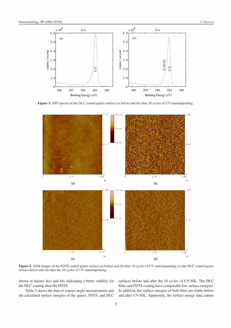
Figure 3. XPS spectra of the DLC coated quartz surface (a) before and (b) after 10 cycles of UV nanoimprinting.
(a) (b)
(c) (d)
Figure 4. AFM images of the FDTS coated quartz surface (a) before and (b) after 10 cycles of UV nanoimprinting; (c) the DLC coated quartzsurface before and (d) after the 10 cycles of UV nanoimprinting.
shown in figures 4(c) and (d), indicating a better stability forthe DLC coating than the FDTS.
Table 3 shows the data of contact angle measurements andthe calculated surface energies of the quartz, FDTS, and DLC
surfaces before and after the 10 cycles of UV-NIL. The DLCfilms and FDTS coating have comparable low surface energies.In addition, the surface energies of both films are stable beforeand after UV-NIL. Apparently, the surface energy data cannot
5

Nanotechnology 19 (2008) 105302 L Tao et al
(a) (b)
Figure 5. AFM images of (a) the nanostructured DLC template with 40 nm wide 100 nm deep gratings and (b) the imprinted SU-8 structures.
Table 3. Contact angles and calculated surface energies for theFDTS and DLC films before and after the UV-NIL and for theUV-cured SU-8 resist.
Contact angle (deg)
Surface energya
(γ = γ d + γ p)(mJ m−2)
Samples H2O Ethylene glycol γ p γ d γ
FDTS0 91.6 ± 0.7 63.0 ± 0.9 2.3 27.5 29.8FDTS10 92.4 ± 0.9 65.5 ± 1.0 2.6 24.9 27.5DLC0 66.4 ± 0.9 45.8 ± 0.9 21.7 14.4 36.1DLC10 63.4 ± 0.7 44.5 ± 0.5 25.6 12.6 38.2Quartz 32.5 ± 0.7 25.5 ± 1.2 67.0 3.5 70.5Cured SU-8 80.0 ± 0.7 43.0 ± 0.5 4.0 37.2 41.2
a Surface energy γ is the sum of γ d (dispersion or non-polarcomponent) and γ p (polar component).
reveal the microscopic damage to the FDTS films, as shown inprevious sections. However, it does provide information aboutthe resist adhesion to the templates and the energy neededto release the template from the resist. The adhesion energy(WAB) between the template and resist can be estimated usingthe Owens and Wendt geometric mean approach [9]:
WAB∼=
√γ
pA · γ p
B +√
γ dA · γ d
B (1)
where γ p and γ d represent the polar and dispersive (or non-polar) components, respectively, of the surface energies of thetwo materials in contact. The adhesion energies of cured SU-8to FDTS (WFDTS/SU−8) and to DLC (WDLC/SU−8) are calculatedto be 33.7 mJ m−2 and 31.7 mJ m−2, respectively, by pluggingcorresponding values from table 3 into equation (1). It showsthat the adhesion energy of SU-8 to the DLC films is slightlylower than that of the FDTS although the DLC has a highersurface energy than FDTS. Therefore, the DLC templates areactually easier (or at least similar) to separate from the curedSU-8 than FDTS, as observed in the imprint experiments. The
adhesion of resist to the template is highly resist dependent.Most resists have a high non-polar component and thereforewould have low adhesion to DLC films since the DLC hasa small non-polar surface energy, resulting in better releaseperformance than FDTS. Similar experimental observation isreported for UV-cured methacrylate, vinyl ether, and acrylateresists [7].
3.4. UV-NIL using nanostructured DLC templates
The AFM image in figure 5(a) shows 40 nm wide and 100 nmdeep gratings fabricated in 300 nm thick DLC films usingEBL, followed by metal lift-off and ICP etching, as describedpreviously. The DLC etch rate was about 100 nm min−1
and the roughness of the film was nearly the same beforeand after the etching [8]. The results demonstrate thatdirect nanopatterning of DLC is feasible and advantageouscompared to the deposition of DLC on patterned quartz,which has relatively non-uniform step coverage and poor filmstability due to higher interfacial stress and wearing. UVnanoimprinting processes were carried out with the patternedDLC template. Figure 5(b) shows the imprinted SU-8 gratings,which are measured with similar dimensions to the template,indicating good pattern transfer fidelity of the imprint process.The template release from the cured SU-8 structures is easy andno obvious pattern distortion has been observed. The patternedDLC templates have been constantly used for more than 6months and their surface energies and film roughness are quitestable.
As shown in figure 1, the UV transmittance varies withDLC thickness and therefore the patterned DLC templateswill result in spatially non-uniform UV exposure to the resistunderneath. Such issues can be alleviated by depositing filmsusing inductive plasmas with very low pressure and narrowerion energy distribution, as discussed in section 3.1. Moreover,the effect of this non-uniform exposure on pattern formationin resist is not significant since the resist patterns are defined
6
Nanotechnology 19 (2008) 105302 L Tao et al
by polymer filling to the template concaves not by the UVexposure as in photolithography. In nanoimprinting, the UVexposure is only used to cure resist patterns and the exposuretime was chosen to ensure that the resist under the thickDLC patterns gets a sufficient dose. In addition, DLC filmsare known to be excellent candidates as protective coatingson things like magnetic hard drives, primarily because thehardness of films above a few nm does not show significantdependence on the thickness [11]. Hence the uniformity of thehardness with thickness may not be a problem for structureswith spatial variation in thickness.
4. Summary
Fluorinated SAM-coated quartz templates were found to bechemically reactive to the radicals generated from the SU-8 resist under UV exposure, resulting in film degradationand roughened surfaces after only 10 cycles of a UVnanoimprinting processes. This kind of irreversible chemicaldamage limits the future applications of F-SAMS as templaterelease coatings for nanoimprint lithography. DLC filmswere investigated as a promising alternative template material.DLC films were deposited on the quartz templates usingplasma enhanced chemical vapor deposition and characterizedusing XPS and AFM before and after UV nanoimprinting incomparison to the FDTS films. The elemental composition,surface roughness, and surface energy of the DLC films arequite stable. The adhesion energy of the DLC template toSU-8 is smaller than that of FDTS despite its slightly highersurface energy. DLC templates with 40–50 nm feature sizewere fabricated using EBL followed by Cr lift-off and ICPetching. UV nanoimprinting using patterned DLC templates inSU-8 shows excellent pattern transfer fidelity at the nanoscale.We believe the DLC material is a promising coating layer and
can also be directly patterned as nanoimprint templates withhigh chemical stability and high wear resistance.
Acknowledgments
The authors would like to thank Professor Robert M Wallaceand student Bongki Lee at The University of Texas at Dallasfor the discussion on XPS spectrum analysis.
References
[1] 2003–2006 International Technology Roadmap forSemiconductors http://www.public.net/itrs
[2] Colburn M et al 1999 Proc. SPIE 3676 379[3] Bailey T, Choi B J, Colburn M, Meissl M, Shaya S, Ekerdt J G,
Sreenivasan S V and Willson C G 2000 J. Vac. Sci. Technol.B 18 3572
[4] Otto M, Bender M, Richter F, Hadam B, Kleim T, Jede R,Spangenberg B and Kurz H 2004 Microelectron. Eng.73/74 152
[5] Jung GY, Li Z, Wu W, Chen Y, Olynick D L, Wang S Y,Tong W M and Williams R S 2005 Langmuir 21 1158
[6] Houle F A, Guyer E, Miller D C, Dauskardt R, Rice E andHamilton J 2006 Proc. SPIE 6153 61531B
[7] Houle F A, Rettner C T, Miller D C andSooriyakumaran R 2007 Appl. Phys. Lett. 90 213103
[8] Ramachandran S, Tao L, Lee T H, Sant S, Overzet L J,Goeckner M J, Kim M J, Lee G S and Hu W 2006 J. Vac.Sci. Technol. B 24 2993
[9] Owens D K and Wendt R C 1969 J. Appl. Polym. Sci. 13 1741[10] Hu W, Bernstein G H, Sarveswaran K and Lieberman M 2004
J. Vac. Sci. Technol. B 22 1711[11] Robertson J 2002 J. Mater. Sci. Eng. R 37 129[12] Tripp C P, Veregin R P N and Hair M L 1993 Langmuir 9 3518[13] Tasker S, Chambers R D and Badyal J P S 1994 J. Phys. Chem.
98 12442[14] Morgan A M, Evans B and Kells J 1995 Langmuir 11 4393[15] Kochi J (ed) 1973 Free Radicals (New York:
Wiley–Interscience)
7