
DRV8711 Stepper Motor Controller IC (Rev. G) - TI.com · STEP DRV8711 SLEEPn SPI 8.0 V to 52 V MCU...
45
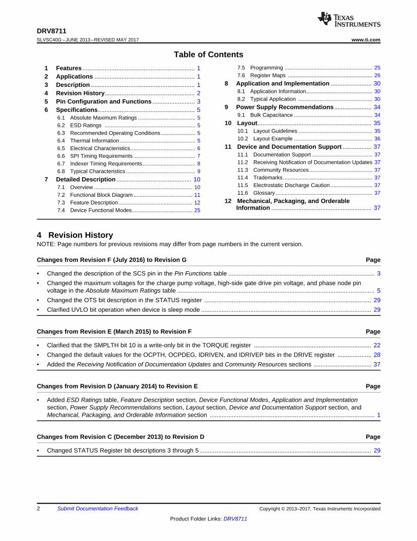
DRV8711 STEP SLEEPn SPI 8.0 V to 52 V MCU + - 1/256 μstep Stepper Motor Pre-Driver DIR nFAULT M + - N-Channel MOSFETs Sense Gate Drive Product Folder Order Now Technical Documents Tools & Software Support & Community Reference Design An IMPORTANT NOTICE at the end of this data sheet addresses availability, warranty, changes, use in safety-critical applications, intellectual property matters and other important disclaimers. PRODUCTION DATA. DRV8711 SLVSC40G – JUNE 2013 – REVISED MAY 2017 DRV8711 Stepper Motor Controller IC 1 1 Features 1• Pulse Width Modulation (PWM) Microstepping Motor Driver – Built-In 1/256-Step Microstepping Indexer – Drives External N-Channel MOSFETs – Optional STEP/DIR Pins – Optional PWM Control Interface for DC Motors • Flexible Decay Modes, Including Automatic Mixed Decay Mode • Stall Detection With Optional BEMF Output • Highly Configurable SPI Serial Interface • Internal Reference and Torque DAC • 8-V to 52-V Operating Supply Voltage Range • Scalable Output Current • Thermally Enhanced Surface-Mount Package • 5-V Regulator Capable of 10-mA Load • Protection and Diagnostic Features – Overcurrent Protection (OCP) – Overtemperature Shutdown (OTS) – Undervoltage Lockout (UVLO) – Individual Fault Condition Indication Bits – Fault Condition Indication Pin 2 Applications • Office Automation Machines • Factory Automation • Textile Machines • Robotics 3 Description The DRV8711 device is a stepper motor controller that uses external N-channel MOSFETs to drive a bipolar stepper motor or two brushed DC motors. A microstepping indexer is integrated, which is capable of step modes from full step to 1/256-step. An ultra-smooth motion profile can be achieved using adaptive blanking time and various current decay modes, including an auto-mixed decay mode. Motor stall is reported with an optional back-EMF output. A simple step/direction or PWM interface allows easy interfacing to controller circuits. A SPI serial interface is used to program the device operation. Output current (torque), step mode, decay mode, and stall detection functions are all programmable through a SPI serial interface. Internal shutdown functions are provided for overcurrent protection, short-circuit protection, undervoltage lockout, and overtemperature. Fault conditions are indicated through a FAULTn pin, and each fault condition is reported through a dedicated bit through SPI. The DRV8711 is packaged in a PowerPAD™ 38-pin HTSSOP package with thermal pad (Eco-friendly: RoHS and no Sb/Br). Device Information (1) PART NUMBER PACKAGE BODY SIZE (NOM) DRV8711 HTSSOP (38) 9.70 mm × 4.40 mm (1) For all available packages, see the orderable addendum at the end of the data sheet. Simplified Schematic
Transcript of DRV8711 Stepper Motor Controller IC (Rev. G) - TI.com · STEP DRV8711 SLEEPn SPI 8.0 V to 52 V MCU...

DRV8711STEP
SLEEPn
SPI
8.0 V to 52 V
MC
U
+ -
1/256 µstep
Stepper Motor
Pre-Driver
DIR
nFAULT
M
+ -
N-C
hann
elM
OS
FE
Ts
Sense
Gate Drive
Product
Folder
Order
Now
Technical
Documents
Tools &
Software
Support &Community
ReferenceDesign
An IMPORTANT NOTICE at the end of this data sheet addresses availability, warranty, changes, use in safety-critical applications,intellectual property matters and other important disclaimers. PRODUCTION DATA.
DRV8711SLVSC40G –JUNE 2013–REVISED MAY 2017
DRV8711 Stepper Motor Controller IC
1
1 Features1• Pulse Width Modulation (PWM) Microstepping
Motor Driver– Built-In 1/256-Step Microstepping Indexer– Drives External N-Channel MOSFETs– Optional STEP/DIR Pins– Optional PWM Control Interface for DC Motors
• Flexible Decay Modes, Including Automatic MixedDecay Mode
• Stall Detection With Optional BEMF Output• Highly Configurable SPI Serial Interface• Internal Reference and Torque DAC• 8-V to 52-V Operating Supply Voltage Range• Scalable Output Current• Thermally Enhanced Surface-Mount Package• 5-V Regulator Capable of 10-mA Load• Protection and Diagnostic Features
– Overcurrent Protection (OCP)– Overtemperature Shutdown (OTS)– Undervoltage Lockout (UVLO)– Individual Fault Condition Indication Bits– Fault Condition Indication Pin
2 Applications• Office Automation Machines• Factory Automation• Textile Machines• Robotics
3 DescriptionThe DRV8711 device is a stepper motor controllerthat uses external N-channel MOSFETs to drive abipolar stepper motor or two brushed DC motors. Amicrostepping indexer is integrated, which is capableof step modes from full step to 1/256-step.
An ultra-smooth motion profile can be achieved usingadaptive blanking time and various current decaymodes, including an auto-mixed decay mode. Motorstall is reported with an optional back-EMF output.
A simple step/direction or PWM interface allows easyinterfacing to controller circuits. A SPI serial interfaceis used to program the device operation. Outputcurrent (torque), step mode, decay mode, and stalldetection functions are all programmable through aSPI serial interface.
Internal shutdown functions are provided forovercurrent protection, short-circuit protection,undervoltage lockout, and overtemperature. Faultconditions are indicated through a FAULTn pin, andeach fault condition is reported through a dedicatedbit through SPI.
The DRV8711 is packaged in a PowerPAD™ 38-pinHTSSOP package with thermal pad (Eco-friendly:RoHS and no Sb/Br).
Device Information(1)
PART NUMBER PACKAGE BODY SIZE (NOM)DRV8711 HTSSOP (38) 9.70 mm × 4.40 mm
(1) For all available packages, see the orderable addendum atthe end of the data sheet.
Simplified Schematic
2
DRV8711SLVSC40G –JUNE 2013–REVISED MAY 2017 www.ti.com
Product Folder Links: DRV8711
Submit Documentation Feedback Copyright © 2013–2017, Texas Instruments Incorporated
Table of Contents1 Features .................................................................. 12 Applications ........................................................... 13 Description ............................................................. 14 Revision History..................................................... 25 Pin Configuration and Functions ......................... 36 Specifications......................................................... 5
6.1 Absolute Maximum Ratings ...................................... 56.2 ESD Ratings ............................................................ 56.3 Recommended Operating Conditions....................... 56.4 Thermal Information .................................................. 56.5 Electrical Characteristics........................................... 66.6 SPI Timing Requirements ......................................... 76.7 Indexer Timing Requirements................................... 86.8 Typical Characteristics .............................................. 9
7 Detailed Description ............................................ 107.1 Overview ................................................................. 107.2 Functional Block Diagram ....................................... 117.3 Feature Description................................................. 127.4 Device Functional Modes........................................ 25
7.5 Programming .......................................................... 257.6 Register Maps ........................................................ 26
8 Application and Implementation ........................ 308.1 Application Information............................................ 308.2 Typical Application ................................................. 30
9 Power Supply Recommendations ...................... 349.1 Bulk Capacitance .................................................... 34
10 Layout................................................................... 3510.1 Layout Guidelines ................................................. 3510.2 Layout Example .................................................... 36
11 Device and Documentation Support ................. 3711.1 Documentation Support ........................................ 3711.2 Receiving Notification of Documentation Updates 3711.3 Community Resources.......................................... 3711.4 Trademarks ........................................................... 3711.5 Electrostatic Discharge Caution............................ 3711.6 Glossary ................................................................ 37
12 Mechanical, Packaging, and OrderableInformation ........................................................... 37
4 Revision HistoryNOTE: Page numbers for previous revisions may differ from page numbers in the current version.
Changes from Revision F (July 2016) to Revision G Page
• Changed the description of the SCS pin in the Pin Functions table ...................................................................................... 3• Changed the maximum voltages for the charge pump voltage, high-side gate drive pin voltage, and phase node pin
voltage in the Absolute Maximum Ratings table .................................................................................................................... 5• Changed the OTS bit description in the STATUS register .................................................................................................. 29• Clarified UVLO bit operation when device is sleep mode .................................................................................................... 29
Changes from Revision E (March 2015) to Revision F Page
• Clarified that the SMPLTH bit 10 is a write-only bit in the TORQUE register ..................................................................... 22• Changed the default values for the OCPTH, OCPDEG, IDRIVEN, and IDRIVEP bits in the DRIVE register .................... 28• Added the Receiving Notification of Documentation Updates and Community Resources sections .................................. 37
Changes from Revision D (January 2014) to Revision E Page
• Added ESD Ratings table, Feature Description section, Device Functional Modes, Application and Implementationsection, Power Supply Recommendations section, Layout section, Device and Documentation Support section, andMechanical, Packaging, and Orderable Information section ................................................................................................. 1
Changes from Revision C (December 2013) to Revision D Page
• Changed STATUS Register bit descriptions 3 through 5..................................................................................................... 29
1
2
3
4
5
6
7
8
9
10
11
12
13
14 25
26
27
28
29
38
37
36
35
34
33
32
31
30
CP1
15
16
17
18
19 20
21
22
23
24
CP2VCP
VMGND
V5
SLEEPnRESET
VINT
STEP / AIN1
BIN2SCLK
SDATI
SDATOFAULTn
STALLn / BEMFVn BEMF
GNDAOUT1A1HSA1LSAISENPAISENNA2LSA2HSAOUT2GNDBOUT1B1HSB1LSBISENPBISENNB2LSB2HSBOUT2
GND
(PPAD)DIR / AIN2BIN1
SCS
3
DRV8711www.ti.com SLVSC40G –JUNE 2013–REVISED MAY 2017
Product Folder Links: DRV8711
Submit Documentation FeedbackCopyright © 2013–2017, Texas Instruments Incorporated
(1) Directions: I = input, O = output, OZ = 3-state output, OD = open-drain output, IO = input/output
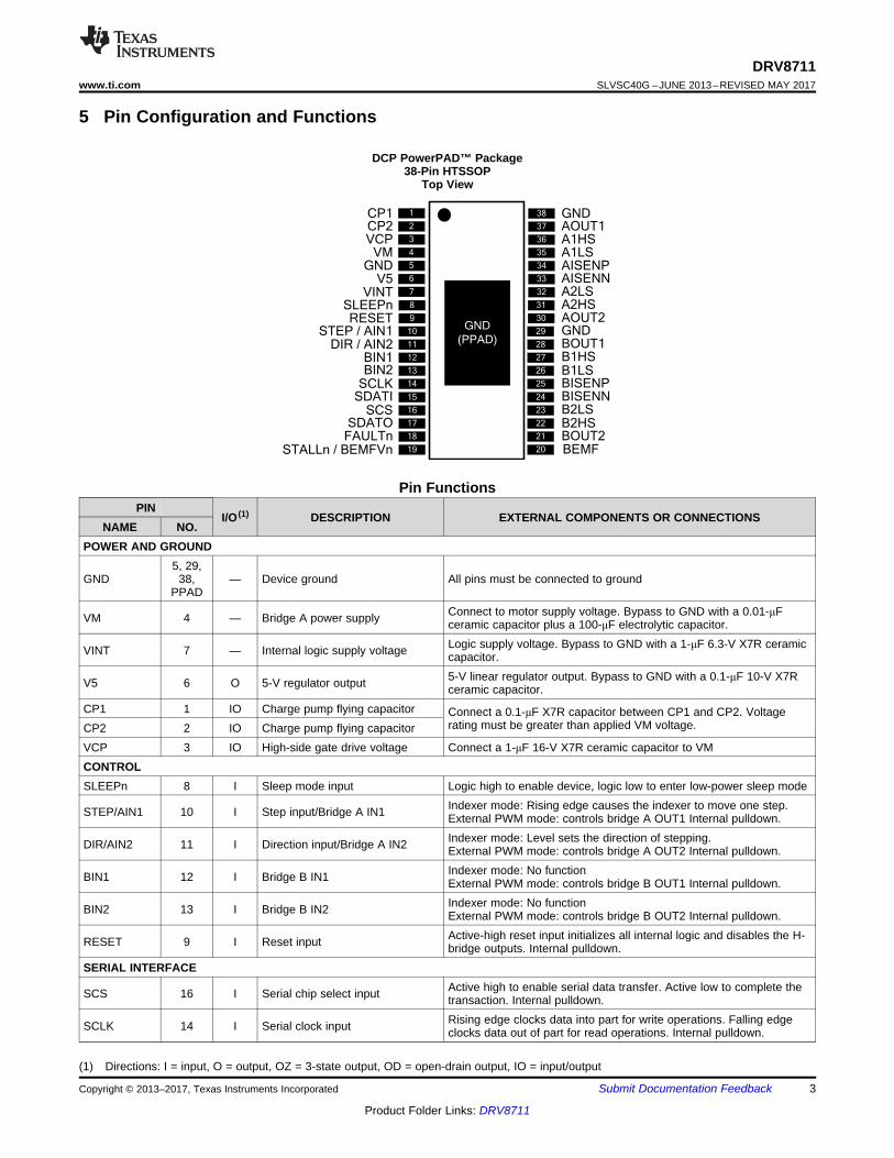
5 Pin Configuration and Functions
DCP PowerPAD™ Package38-Pin HTSSOP
Top View
Pin FunctionsPIN
I/O (1) DESCRIPTION EXTERNAL COMPONENTS OR CONNECTIONSNAME NO.
POWER AND GROUND
GND5, 29,
38,PPAD
— Device ground All pins must be connected to ground
VM 4 — Bridge A power supply Connect to motor supply voltage. Bypass to GND with a 0.01-μFceramic capacitor plus a 100-μF electrolytic capacitor.
VINT 7 — Internal logic supply voltage Logic supply voltage. Bypass to GND with a 1-μF 6.3-V X7R ceramiccapacitor.
V5 6 O 5-V regulator output 5-V linear regulator output. Bypass to GND with a 0.1-μF 10-V X7Rceramic capacitor.
CP1 1 IO Charge pump flying capacitor Connect a 0.1-μF X7R capacitor between CP1 and CP2. Voltagerating must be greater than applied VM voltage.CP2 2 IO Charge pump flying capacitor
VCP 3 IO High-side gate drive voltage Connect a 1-μF 16-V X7R ceramic capacitor to VMCONTROLSLEEPn 8 I Sleep mode input Logic high to enable device, logic low to enter low-power sleep mode
STEP/AIN1 10 I Step input/Bridge A IN1 Indexer mode: Rising edge causes the indexer to move one step.External PWM mode: controls bridge A OUT1 Internal pulldown.
DIR/AIN2 11 I Direction input/Bridge A IN2 Indexer mode: Level sets the direction of stepping.External PWM mode: controls bridge A OUT2 Internal pulldown.
BIN1 12 I Bridge B IN1 Indexer mode: No functionExternal PWM mode: controls bridge B OUT1 Internal pulldown.
BIN2 13 I Bridge B IN2 Indexer mode: No functionExternal PWM mode: controls bridge B OUT2 Internal pulldown.
RESET 9 I Reset input Active-high reset input initializes all internal logic and disables the H-bridge outputs. Internal pulldown.
SERIAL INTERFACE
SCS 16 I Serial chip select input Active high to enable serial data transfer. Active low to complete thetransaction. Internal pulldown.
SCLK 14 I Serial clock input Rising edge clocks data into part for write operations. Falling edgeclocks data out of part for read operations. Internal pulldown.

4
DRV8711SLVSC40G –JUNE 2013–REVISED MAY 2017 www.ti.com
Product Folder Links: DRV8711
Submit Documentation Feedback Copyright © 2013–2017, Texas Instruments Incorporated
Pin Functions (continued)PIN
I/O (1) DESCRIPTION EXTERNAL COMPONENTS OR CONNECTIONSNAME NO.
SDATI 15 I Serial data input Serial data input from controller. Internal pulldown.
SDATO 17 OD Serial data output Serial data output to controller. Open-drain output requires externalpullup.
STATUS
STALLn/BEMFVn 19 OD Stall/Back EMF valid
Internal stall detect mode: logic low when motor stall detected.External stall detect mode: Active low when valid back EMFmeasurement is ready.Open-drain output requires external pullup.
FAULTn 18 OD FaultLogic low when in fault condition. Open-drain output requires externalpullup.Faults: OCP, PDF, OTS, UVLO
BEMF 20 O Back EMF Analog output voltage represents motor back EMF. Place a 1-nF low-leakage capacitor to ground on this pin.
OUTPUTSA1HS 36 O Bridge A out 1 HS gate Connect to gate of HS FET for bridge A out 1AOUT1 37 I Bridge A output 1 Connect to output node of external FETs of bridge A out 1A1LS 35 O Bridge A out 1 LS gate Connect to gate of LS FET for bridge A out 1A2HS 31 O Bridge A out 2 HS gate Connect to gate of HS FET for bridge A out 2AOUT2 30 I Bridge A output 2 Connect to output node of external FETs of bridge A out 2A2LS 32 O Bridge A out 2 LS gate Connect to gate of LS FET for bridge A out 2AISENP 34 I Bridge A Isense + in Connect to current sense resistor for bridge AAISENN 33 I Bridge A Isense – in Connect to ground at current sense resistor for bridge AB1HS 27 O Bridge B out 1 HS gate Connect to gate of HS FET for bridge B out 1BOUT1 28 I Bridge B output 1 Connect to output node of external FETs of bridge B out 1B1LS 26 O Bridge B out 1 LS gate Connect to gate of LS FET for bridge B out 1B2HS 22 O Bridge B out 2 HS gate Connect to gate of HS FET for bridge B out 2BOUT2 21 I Bridge B output 2 Connect to output node of external FETs of bridge B out 2B2LS 23 O Bridge B out 2 LS gate Connect to gate of LS FET for bridge B out 2BISENP 25 I Bridge B Isense + in Connect to current sense resistor for bridge BBISENN 24 I Bridge B Isense – in Connect to ground at current sense resistor for bridge B
5
DRV8711www.ti.com SLVSC40G –JUNE 2013–REVISED MAY 2017
Product Folder Links: DRV8711
Submit Documentation FeedbackCopyright © 2013–2017, Texas Instruments Incorporated
(1) Stresses beyond those listed under Absolute Maximum Ratings may cause permanent damage to the device. These are stress ratingsonly, which do not imply functional operation of the device at these or any other conditions beyond those indicated under RecommendedOperating Conditions. Exposure to absolute-maximum-rated conditions for extended periods may affect device reliability.
(2) All voltage values are with respect to network ground terminal.(3) Power dissipation and thermal limits must be observed.
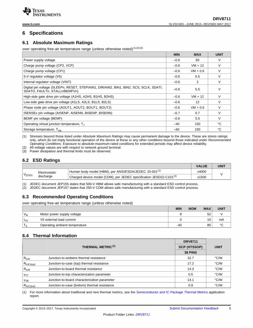
6 Specifications
6.1 Absolute Maximum Ratingsover operating free-air temperature range (unless otherwise noted) (1) (2) (3)
MIN MAX UNITPower supply voltage –0.6 60 VCharge pump voltage (CP2, VCP) –0.6 VM + 12 VCharge pump voltage (CP1) –0.6 VM + 0.6 V5-V regulator voltage (V5) –0.6 5.5 VInternal regulator voltage (VINT) –0.6 2 VDigital pin voltage (SLEEPn, RESET, STEP/AIN1, DIR/AIN2, BIN1, BIN2, SCS, SCLK, SDATI,SDATO, FAULTn, STALLn/BEMFVn) –0.6 5.5 V
High-side gate drive pin voltage (A1HS, A2HS, B1HS, B2HS) –0.6 VM + 12 VLow-side gate drive pin voltage (A1LS, A2LS, B1LS, B2LS) –0.6 12 VPhase node pin voltage (AOUT1, AOUT2, BOUT1, BOUT2) –0.6 VM + 0.6 VISENSEx pin voltage (AISENP, AISENN, BISENP, BISENN) –0.7 0.7 VBEMF pin voltage (BEMF) –0.6 5.5 VOperating virtual junction temperature, TJ –40 150 °CStorage temperature, Tstg –60 150 °C
(1) JEDEC document JEP155 states that 500-V HBM allows safe manufacturing with a standard ESD control process.(2) JEDEC document JEP157 states that 250-V CDM allows safe manufacturing with a standard ESD control process.
6.2 ESD RatingsVALUE UNIT
V(ESD)Electrostaticdischarge
Human body model (HBM), per ANSI/ESDA/JEDEC JS-001 (1) ±4000V
Charged device model (CDM), per JEDEC specification JESD22-C101 (2) ±1500
6.3 Recommended Operating Conditionsover operating free-air temperature range (unless otherwise noted)
MIN NOM MAX UNITVM Motor power supply voltage 8 52 VIVS V5 external load current 0 10 mATA Operating ambient temperature -40 85 °C
(1) For more information about traditional and new thermal metrics, see the Semiconductor and IC Package Thermal Metrics applicationreport.
6.4 Thermal Information
THERMAL METRIC (1)DRV8711
UNITDCP (HTSSOP)38 PINS
RθJA Junction-to-ambient thermal resistance 32.7 °C/WRθJC(top) Junction-to-case (top) thermal resistance 17.2 °C/WRθJB Junction-to-board thermal resistance 14.3 °C/WψJT Junction-to-top characterization parameter 0.5 °C/WψJB Junction-to-board characterization parameter 14.1 °C/WRθJC(bot) Junction-to-case (bottom) thermal resistance 0.9 °C/W
6
DRV8711SLVSC40G –JUNE 2013–REVISED MAY 2017 www.ti.com
Product Folder Links: DRV8711
Submit Documentation Feedback Copyright © 2013–2017, Texas Instruments Incorporated
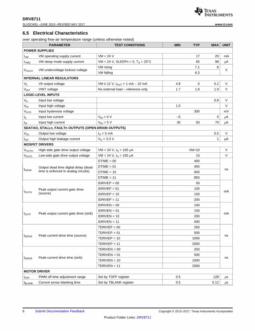
6.5 Electrical Characteristicsover operating free-air temperature range (unless otherwise noted)
PARAMETER TEST CONDITIONS MIN TYP MAX UNITPOWER SUPPLIESIVM VM operating supply current VM = 24 V 17 20 mAIVMQ VM sleep mode supply current VM = 24 V, SLEEPn = 0, TA = 25°C 65 98 μA
VUVLO VM undervoltage lockout voltageVM rising 7.1 8
VVM falling 6.3
INTERNAL LINEAR REGULATORSV5 V5 output voltage VM ≥ 12 V, IOUT = 1 mA – 10 mA 4.8 5 5.2 VVINT VINT voltage No external load – reference only 1.7 1.8 1.9 VLOGIC-LEVEL INPUTSVIL Input low voltage 0.8 VVIH Input high voltage 1.5 VVHYS Input hysteresis voltage 300 mVIIL Input low current VIN = 0 V –5 5 μAIIH Input high current VIN = 5 V 30 50 70 μASDATAO, STALLn, FAULTn OUTPUTS (OPEN-DRAIN OUTPUTS)VOL Output low voltage IO = 5 mA 0.5 VIOH Output high leakage current VO = 3.3 V 1 µAMOSFET DRIVERSVOUTH High-side gate drive output voltage VM = 24 V, IO = 100 μA VM+10 VVOUTL Low-side gate drive output voltage VM = 24 V, IO = 100 μA 10 V
tDEADOutput dead time digital delay (deadtime is enforced in analog circuits)
DTIME = 00 400
nsDTIME = 01 450DTIME = 10 650DTIME = 11 850
IOUTHPeak output current gate drive(source)
IDRIVEP = 00 50
mAIDRIVEP = 01 100IDRIVEP = 10 150IDRIVEP = 11 200
IOUTl Peak output current gate drive (sink)
IDRIVEN = 00 100
mAIDRIVEN = 01 150IDRIVEN = 10 200IDRIVEN = 11 400
tDRIVE Peak current drive time (source)
TDRIVEP = 00 250
nsTDRIVEP = 01 500TDRIVEP = 10 1000TDRIVEP = 11 2000
tDRIVE Peak current drive time (sink)
TDRIVEN = 00 250
nsTDRIVEN = 01 500TDRIVEN = 10 1000TDRIVEN = 11 2000
MOTOR DRIVERtOFF PWM off time adjustment range Set by TOFF register 0.5 128 μstBLANK Current sense blanking time Set by TBLANK register 0.5 5.12 μs
7
DRV8711www.ti.com SLVSC40G –JUNE 2013–REVISED MAY 2017
Product Folder Links: DRV8711
Submit Documentation FeedbackCopyright © 2013–2017, Texas Instruments Incorporated
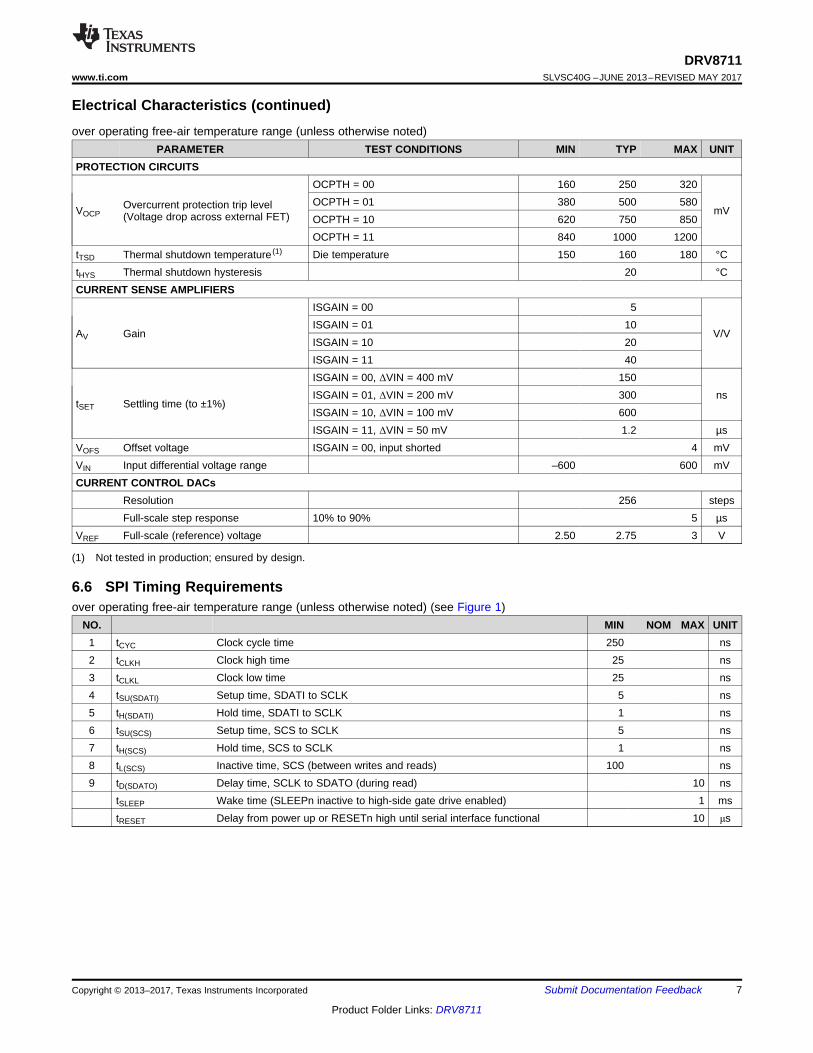
Electrical Characteristics (continued)over operating free-air temperature range (unless otherwise noted)
PARAMETER TEST CONDITIONS MIN TYP MAX UNIT
(1) Not tested in production; ensured by design.
PROTECTION CIRCUITS
VOCPOvercurrent protection trip level(Voltage drop across external FET)
OCPTH = 00 160 250 320
mVOCPTH = 01 380 500 580OCPTH = 10 620 750 850OCPTH = 11 840 1000 1200
tTSD Thermal shutdown temperature (1) Die temperature 150 160 180 °CtHYS Thermal shutdown hysteresis 20 °CCURRENT SENSE AMPLIFIERS
AV Gain
ISGAIN = 00 5
V/VISGAIN = 01 10ISGAIN = 10 20ISGAIN = 11 40
tSET Settling time (to ±1%)
ISGAIN = 00, ΔVIN = 400 mV 150nsISGAIN = 01, ΔVIN = 200 mV 300
ISGAIN = 10, ΔVIN = 100 mV 600ISGAIN = 11, ΔVIN = 50 mV 1.2 µs
VOFS Offset voltage ISGAIN = 00, input shorted 4 mVVIN Input differential voltage range –600 600 mVCURRENT CONTROL DACs
Resolution 256 stepsFull-scale step response 10% to 90% 5 µs
VREF Full-scale (reference) voltage 2.50 2.75 3 V
6.6 SPI Timing Requirementsover operating free-air temperature range (unless otherwise noted) (see Figure 1)
NO. MIN NOM MAX UNIT1 tCYC Clock cycle time 250 ns2 tCLKH Clock high time 25 ns3 tCLKL Clock low time 25 ns4 tSU(SDATI) Setup time, SDATI to SCLK 5 ns5 tH(SDATI) Hold time, SDATI to SCLK 1 ns6 tSU(SCS) Setup time, SCS to SCLK 5 ns7 tH(SCS) Hold time, SCS to SCLK 1 ns8 tL(SCS) Inactive time, SCS (between writes and reads) 100 ns9 tD(SDATO) Delay time, SCLK to SDATO (during read) 10 ns
tSLEEP Wake time (SLEEPn inactive to high-side gate drive enabled) 1 mstRESET Delay from power up or RESETn high until serial interface functional 10 μs

STEP
DIR, MODE
2 3
1
4 5
XX
SCLK
SDATI
1
3
4
2
SCS
5
6 7 8
SDATOSDATO
valid
9
8
DRV8711SLVSC40G –JUNE 2013–REVISED MAY 2017 www.ti.com
Product Folder Links: DRV8711
Submit Documentation Feedback Copyright © 2013–2017, Texas Instruments Incorporated
6.7 Indexer Timing Requirementsover operating free-air temperature range (unless otherwise noted) (see Figure 2)
NO. MIN NOM MAX UNIT1 fSTEP Step frequency 250 kHz2 tWH(STEP) Pulse duration, STEP high 1.9 μs3 tWL(STEP) Pulse duration, STEP low 1.9 μs4 tSU(STEP) Setup time, command to STEP rising 200 ns5 tH(STEP) Hold time, command to STEP rising 200 ns
Figure 1. SPI Timing
Figure 2. Indexer Timing
4
5
6
7
8
9
10
11
12
8 12 16 20 24 28 32 36 40 44 48 52
RD
S(O
N)
HS
+ L
S)
(m
)
Temperature (C)
±40C
25°C
85°C
C007
4.5
4.6
4.7
4.8
4.9
5.0
5.1
5.2
5.3
5.4
5.5
8 12 16 20 24 28 32 36 40 44 48 52
V5
No
Load
Temperature (C)
±40C
25°C
85°C
C008
15.0
15.5
16.0
16.5
17.0
17.5
8 12 16 20 24 28 32 36 40 44 48 52
I VM
(m
A)
VVM (V)
±40C
25°C
85°C
C005
0
40
80
120
160
200
240
8 12 16 20 24 28 32 36 40 44 48 52
I VM
Q (
µA
)
VVM (V)
±40C 25°C85°C
C006
9
DRV8711www.ti.com SLVSC40G –JUNE 2013–REVISED MAY 2017
Product Folder Links: DRV8711
Submit Documentation FeedbackCopyright © 2013–2017, Texas Instruments Incorporated
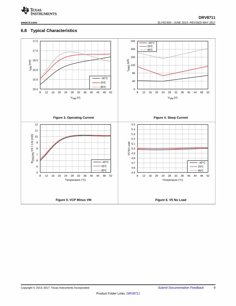
6.8 Typical Characteristics
Figure 3. Operating Current Figure 4. Sleep Current
Figure 5. VCP Minus VM Figure 6. V5 No Load
10
DRV8711SLVSC40G –JUNE 2013–REVISED MAY 2017 www.ti.com
Product Folder Links: DRV8711
Submit Documentation Feedback Copyright © 2013–2017, Texas Instruments Incorporated
7 Detailed Description
7.1 OverviewThe DRV8711 device is a stepper motor controller that uses external N-channel MOSFETs to drive a bipolarstepper motor or two brushed DC motors. A microstepping indexer is integrated, which is capable of step modesfrom full step to 1/256-step.
An ultra-smooth motion profile can be achieved using adaptive blanking time, adjustable decay times, andvarious current decay modes, including an auto-mixed decay mode. When microstepping, motor stall can bereported with an optional back-EMF output.
A simple step/direction or PWM interface allows easy interfacing to controller circuits. A SPI serial interface isused to program the device operation. Output current (torque), step mode, decay mode, and stall detectionfunctions are all programmable through a SPI serial interface.
Internal shutdown functions are provided for overcurrent protection, short-circuit protection, undervoltage lockout,and overtemperature. Fault conditions are indicated through a FAULTn pin, and each fault condition is reportedthrough a dedicated bit through SPI.
Over-
Temp
AOUT1
GND
RESET
Gate
Drive
&
OCP
Step
Motor
SCS
SCLK
VM
VM
SDATO
SDATI
SLEEPn
100 Fµ
+
0.01 Fµ
VM
PWM
logic
FAULTn
VINT
5V OUT
1 Fµ
CP1CP2 VCP
HS Gate DriveCharge
Pump
UVLO
PUCSTEP/AIN1
A1HSVM
A1LS
AOUT2
A2HSVM
A2LS
BOUT1
B1HSVM
B1LS
BOUT2
B2HSVM
B2LS
Gate
Drive
&
OCP
Gate
Drive
&
OCP
Gate
Drive
&
OCP
BISENP
ISEN
amp
+
-
AISENP
Comp
+
-
PWM
logic
STALLn / BEMFVn
DIR/AIN2
Reference
Stall detect BEMF
SIN
DAC
SIN
DAC
+
-
Comp
+
-
ISEN
amp
+
-
Comp
+
-
+
-
Comp
+
-AISENN
BISENN
BIN1
BIN2
0.1 Fµ1 Fµ
Regs
V5
VM
1nF
0.1 Fµ
X
X
Torque
DAC
Torque
DAC
Logic
DCM
DCM
Copyright © 2017, Texas Instruments Incorporated
11
DRV8711www.ti.com SLVSC40G –JUNE 2013–REVISED MAY 2017
Product Folder Links: DRV8711
Submit Documentation FeedbackCopyright © 2013–2017, Texas Instruments Incorporated
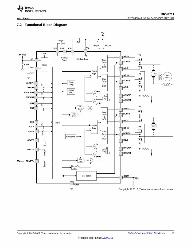
7.2 Functional Block Diagram

12
DRV8711SLVSC40G –JUNE 2013–REVISED MAY 2017 www.ti.com
Product Folder Links: DRV8711
Submit Documentation Feedback Copyright © 2013–2017, Texas Instruments Incorporated
7.3 Feature DescriptionTable 1 lists the critical components for the device.
Table 1. Critical ComponentsPIN NAME COMPONENT
4 VM 100-µF electrolytic rated for VM voltage to GND 0.01-µF ceramic rated for VM voltage to GND3 VCP 1-µF ceramic X7R rated 16 V to VCP
1, 2 CP1, CP2 0.1-µF rated for VM + 12 V between these pins6 V5 0.1-µF ceramic X7R rated 6.3 V to GND7 VINT 1-µF ceramic X7R rated 6.3 V to GND
17 SDATO Requires external pullup to logic supply18 FAULTn Requires external pullup to logic supply19 STALLn/BEMFVn Requires external pullup to logic supply20 BEMF 1-nF low-leakage capacitor to GND
7.3.1 PWM Motor DriversThe DRV8711 contains two H-bridge motor predrivers with current control PWM circuitry. More detaileddescriptions of the subblocks are described in the following sections.
7.3.2 Direct PWM Input ModeDirect PWM mode is selected by setting the PWMMODE bit in the OFF register. In direct PWM input mode, theAIN1, AIN2, BIN1, and BIN2 directly control the state of the output drivers. This allows for driving up to twobrushed DC motors. The logic is shown in Table 2:
Table 2. Direct PWM Input Mode LogicxIN1 xIN2 xOUT1 xOUT2 OPERATION
0 0 Z Z Asynchronous Fast Decay0 1 L H Reverse Drive1 0 H L Forward Drive1 1 L L Slow Decay
If mixed or auto-mixed decay modes are used, they will apply to every cycle, because current change informationis not available.
In direct PWM mode, the current control circuitry is still active. The full-scale VREF is set to 2.75 V. TheTORQUE register may be used to scale this value, and the ISEN sense amp gain may still be set using theISGAIN bits of the CTRL register.

CHOP
ISENSE
2.75V TORQUEI
256 ISGAIN R
·
=
· ·
xOUT1Gate
Drive
&
OCP
PWM
logic
x1HSVM
x1LS
xOUT2
x2HSVM
x2LS
Gate
Drive
&
OCP
ISEN
amp
+
-
xISENP
Comp
+
-
+
-
Comp
+
-
xISENN
X
Torque
DAC
VREF ISGAIN
TORQUE
RISENSE
1 V
xIN1
xIN2
13
DRV8711www.ti.com SLVSC40G –JUNE 2013–REVISED MAY 2017
Product Folder Links: DRV8711
Submit Documentation FeedbackCopyright © 2013–2017, Texas Instruments Incorporated
Figure 7. Direct PWM Input Mode
The current through the motor windings is regulated by an adjustable fixed-off-time PWM current regulationcircuit. When an H-bridge is enabled, current rises through the winding at a rate dependent on the DC voltageand inductance of the winding and the magnitude of the back EMF present. Once the current hits the currentchopping threshold, the bridge disables the current for a fixed period of time, which is programmable between500 ns and 128 µs by writing to the TOFF bits in the OFF register. After the off time expires, the bridge is re-enabled, starting another PWM cycle.
The chopping current is set by a comparator which compares the voltage across a current sense resistorconnected to the xISENx pins, multiplied by the gain of the current sense amplifier, with a reference voltage. Thecurrent sense amplifier is programmable in the CTRL register. When driving in PWM mode, the chopping currentis calculated as follows:
(1)
Where TORQUE is the setting of the TORQUE bits, and ISGAIN is the programmed gain of the ISENSEamplifiers (5, 10, 20, or 40).
14
DRV8711SLVSC40G –JUNE 2013–REVISED MAY 2017 www.ti.com
Product Folder Links: DRV8711
Submit Documentation Feedback Copyright © 2013–2017, Texas Instruments Incorporated
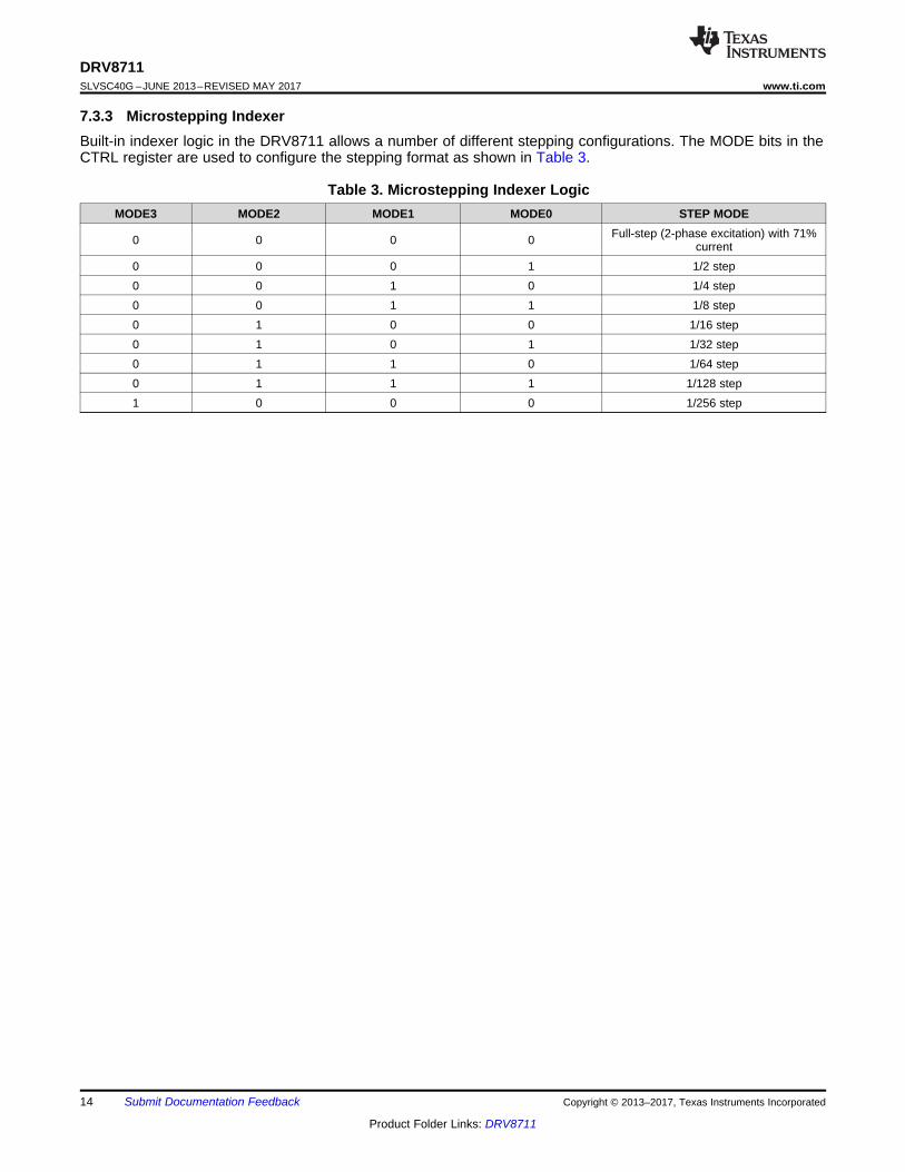
7.3.3 Microstepping IndexerBuilt-in indexer logic in the DRV8711 allows a number of different stepping configurations. The MODE bits in theCTRL register are used to configure the stepping format as shown in Table 3.
Table 3. Microstepping Indexer LogicMODE3 MODE2 MODE1 MODE0 STEP MODE
0 0 0 0 Full-step (2-phase excitation) with 71%current
0 0 0 1 1/2 step0 0 1 0 1/4 step0 0 1 1 1/8 step0 1 0 0 1/16 step0 1 0 1 1/32 step0 1 1 0 1/64 step0 1 1 1 1/128 step1 0 0 0 1/256 step
15
DRV8711www.ti.com SLVSC40G –JUNE 2013–REVISED MAY 2017
Product Folder Links: DRV8711
Submit Documentation FeedbackCopyright © 2013–2017, Texas Instruments Incorporated
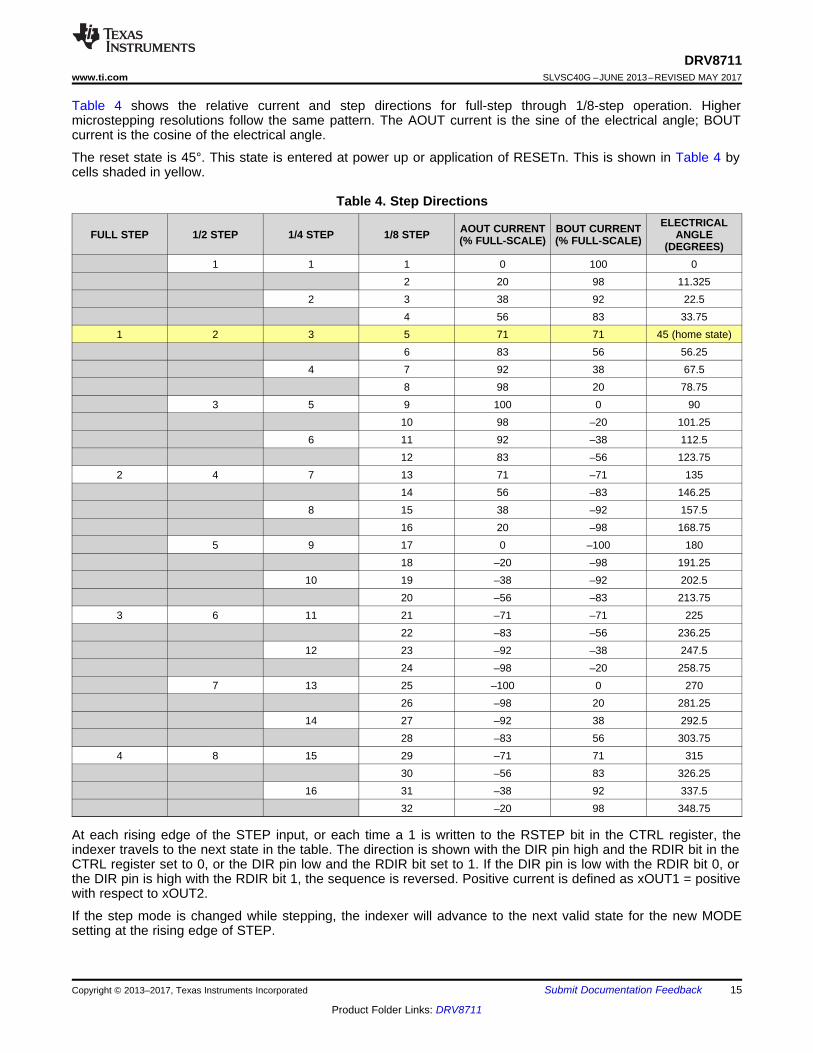
Table 4 shows the relative current and step directions for full-step through 1/8-step operation. Highermicrostepping resolutions follow the same pattern. The AOUT current is the sine of the electrical angle; BOUTcurrent is the cosine of the electrical angle.
The reset state is 45°. This state is entered at power up or application of RESETn. This is shown in Table 4 bycells shaded in yellow.
Table 4. Step Directions
FULL STEP 1/2 STEP 1/4 STEP 1/8 STEP AOUT CURRENT(% FULL-SCALE)
BOUT CURRENT(% FULL-SCALE)
ELECTRICALANGLE
(DEGREES)1 1 1 0 100 0
2 20 98 11.3252 3 38 92 22.5
4 56 83 33.751 2 3 5 71 71 45 (home state)
6 83 56 56.254 7 92 38 67.5
8 98 20 78.753 5 9 100 0 90
10 98 –20 101.256 11 92 –38 112.5
12 83 –56 123.752 4 7 13 71 –71 135
14 56 –83 146.258 15 38 –92 157.5
16 20 –98 168.755 9 17 0 –100 180
18 –20 –98 191.2510 19 –38 –92 202.5
20 –56 –83 213.753 6 11 21 –71 –71 225
22 –83 –56 236.2512 23 –92 –38 247.5
24 –98 –20 258.757 13 25 –100 0 270
26 –98 20 281.2514 27 –92 38 292.5
28 –83 56 303.754 8 15 29 –71 71 315
30 –56 83 326.2516 31 –38 92 337.5
32 –20 98 348.75
At each rising edge of the STEP input, or each time a 1 is written to the RSTEP bit in the CTRL register, theindexer travels to the next state in the table. The direction is shown with the DIR pin high and the RDIR bit in theCTRL register set to 0, or the DIR pin low and the RDIR bit set to 1. If the DIR pin is low with the RDIR bit 0, orthe DIR pin is high with the RDIR bit 1, the sequence is reversed. Positive current is defined as xOUT1 = positivewith respect to xOUT2.
If the step mode is changed while stepping, the indexer will advance to the next valid state for the new MODEsetting at the rising edge of STEP.

xOUT1
Gate Drive
&OCP
PWM logic
x1HSVM
x1LS
xOUT2
x2HSVM
x2LS
Gate Drive
&OCP
ISENamp
+
-
xISENP
Comp
+
-
SIN
DAC
+-
Comp
+
-
xISENN
X
Torque
DAC
Indexer ISGAIN
TORQUE
Registers
RISENSE
2.75 V
1 V
16
DRV8711SLVSC40G –JUNE 2013–REVISED MAY 2017 www.ti.com
Product Folder Links: DRV8711
Submit Documentation Feedback Copyright © 2013–2017, Texas Instruments Incorporated
7.3.4 Current RegulationThe current through the motor windings is regulated by an adjustable fixed-off-time PWM current regulationcircuit. When an H-bridge is enabled, current rises through the winding at a rate dependent on the DC voltageand inductance of the winding and the magnitude of the back EMF present. Once the current hits the currentchopping threshold, the bridge disables the current for a fixed period of time, which is programmable between500 nS and 128 µS by writing to the TOFF bits in the OFF register. After the off time expires, the bridge is re-enabled, starting another PWM cycle.
In stepping motors, current regulation is used to vary the current in the two windings in a sinusoidal fashion toprovide smooth motion.
The PWM chopping current is set by a comparator which compares the voltage across a current sense resistorconnected to the xISENx pins, multiplied by the gain of the current sense amplifier, with a reference voltage. Thecurrent sense amplifier is programmable in the CTRL register.
Figure 8. PWM Chopping Current
To generate the reference voltage for the current chopping comparator, the output of a sine lookup table ismultiplied by the value of the bits in the TORQUE register. This result is applied to a sine-weighted DAC, whosefull-scale output voltage is 2.75 V.
Therefore, the full-scale (100%) chopping current is calculated as follows:
xOUT1 xOUT23
1
2
3
Drive Current
Slow decay (brake)
Fast decay (reverse)
VM
1
2
Slow Decay
Fast Decay
Mixed Decay
PWMON PWM OFF
TOFF
Itrip
TDECAY
TBLANK
FS
ISENSE
2.75V TORQUEI
256 ISGAIN R
·
=
· ·
17
DRV8711www.ti.com SLVSC40G –JUNE 2013–REVISED MAY 2017
Product Folder Links: DRV8711
Submit Documentation FeedbackCopyright © 2013–2017, Texas Instruments Incorporated
where• TORQUE is the setting of the TORQUE bits• ISGAIN is the programmed gain of the ISENSE amplifiers (5, 10, 20, or 40) (2)
Example:
If a 0.1-Ω sense resistor is used, ISGAIN is set to 0 (gain of 5), and TORQUE is set to 255, the full-scale (100%)chopping current will be (2.75 V * 255) / (256 * 5 * 0.1 Ω) = 5.5 A.
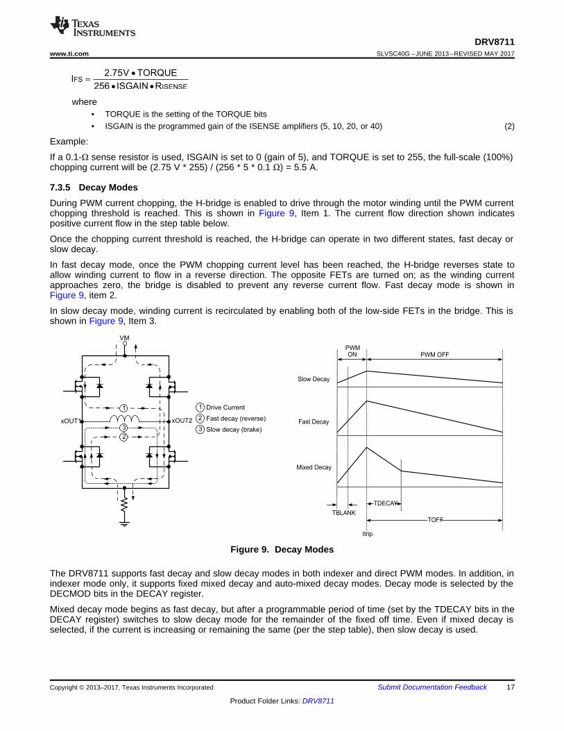
7.3.5 Decay ModesDuring PWM current chopping, the H-bridge is enabled to drive through the motor winding until the PWM currentchopping threshold is reached. This is shown in Figure 9, Item 1. The current flow direction shown indicatespositive current flow in the step table below.
Once the chopping current threshold is reached, the H-bridge can operate in two different states, fast decay orslow decay.
In fast decay mode, once the PWM chopping current level has been reached, the H-bridge reverses state toallow winding current to flow in a reverse direction. The opposite FETs are turned on; as the winding currentapproaches zero, the bridge is disabled to prevent any reverse current flow. Fast decay mode is shown inFigure 9, item 2.
In slow decay mode, winding current is recirculated by enabling both of the low-side FETs in the bridge. This isshown in Figure 9, Item 3.
Figure 9. Decay Modes
The DRV8711 supports fast decay and slow decay modes in both indexer and direct PWM modes. In addition, inindexer mode only, it supports fixed mixed decay and auto-mixed decay modes. Decay mode is selected by theDECMOD bits in the DECAY register.
Mixed decay mode begins as fast decay, but after a programmable period of time (set by the TDECAY bits in theDECAY register) switches to slow decay mode for the remainder of the fixed off time. Even if mixed decay isselected, if the current is increasing or remaining the same (per the step table), then slow decay is used.

tOFFI below Itrip
after tBLANK
I above Itrip
after tBLANK
tBLANK tOFF
tOFFOn
Fast
Decay
Slow
Decay
tBLANK tBLANK
tON
Itrip
tBLANK
tON
Itrip
tOFF
I < ItripAt Itrip and after
tBLANK, slow decay
I > Itrip, start
fast decayWhen I < Itrip in fast decay
and tBLANK expires, change
to slow decay
tON
tBLANK tBLANK
tON
18
DRV8711SLVSC40G –JUNE 2013–REVISED MAY 2017 www.ti.com
Product Folder Links: DRV8711
Submit Documentation Feedback Copyright © 2013–2017, Texas Instruments Incorporated
Auto-mixed decay mode samples the current level at the end of the blanking time, and if the current is above theItrip threshold, immediately changes the H-bridge to fast decay. During fast decay, the (negative) current ismonitored, and when it falls below the Itrip threshold (and another blanking time has passed), the bridge isswitched to slow decay. Once the fixed off time expires, a new cycle is started.
If the bridge is turned on and at the end of TBLANK the current is below the Itrip threshold, the bridge remains onuntil the current reaches Itrip. Then slow decay is entered for the fixed off time, and a new cycle begins.
See Figure 10 and Figure 11.
The upper waveform shows the behavior if I < Itrip at the end of tBLANK. At slow motor speeds, where backEMF is not significant, the current increase during the ON phase is the same magnitude as the current decreasein fast decay, because both times are controlled by tBLANK, and the rate of change is the same (full VM isapplied to the load inductance in both cases, but in opposite directions). In this case, the current will gradually bedriven down until the peak current is just hitting Itrip at the end of the blanking time, after which some cycles willbe slow decay, and some will be mixed decay.
Figure 10. I < Itrip at the End of tBLANK
If the Itrip level changes during a PWM cycle (in response to a step command to the indexer), the current cycle isimmediately terminated, and a new cycle is begun. Refer to the drawing below.
If the Itrip level has increased, the H-bridge will immediately turn on; if the Itrip level has decreased, fast decaymode is begun immediately. The top waveform shows what happens when the Itrip threshold decreases during aPWM cycle. The lower Itrip level results in the current being above the Itrip threshold at the end of tBLANK onthe following cycle. Fast decay is entered until the current is driven below the Itrip threshold.

xOUT1Gate
Drive
andOCP
PWM
logic
x1HSVM
x1LS
xOUT2
x2HSVM
x2LS
Gate
Driveand
OCP
ISEN
amp
+
-
xISENP
Comp
+
-
+
-
Comp
+
-
xISENN
RISENSE
Optional Filtering
R
R
C
tOFFtBLANK
tON
Itrip increase tBLANKtON
Itrip
Itrip decrease tOFFtBLANKtON
Decrease in Itrip terminatescycle, fast decay begins
Itrip
When I< Itrip in fast decaychange to slow decay
tBLANK
tON
tOFF
Increase in Itrip terminatescycle, bridge turns on
On
FastDecay
SlowDecay
19
DRV8711www.ti.com SLVSC40G –JUNE 2013–REVISED MAY 2017
Product Folder Links: DRV8711
Submit Documentation FeedbackCopyright © 2013–2017, Texas Instruments Incorporated
Figure 11. Itrip Level Changing During a PWM Cycle
To accurately detect zero current, an internal offset has been intentionally placed in the zero current detectioncircuit. If an external filter is placed on the current sense resistor to the xISENN and xISENP pins, symmetrymust be maintained. This means that any resistance between the bottom of the RISENSE resistor and xISENNmust be matched by the same resistor value (1% tolerance) between the top of the RISENSE resistor and xISENP.Ensure a maximum resistance of 500 Ω. The capacitor value should be chosen such that the RC time constant isbetween 50 ns and 60 ns. Any external filtering on these pins is optional and not required for operation.
Figure 12. Optional Filtering Between RISENSE and xINSENx
7.3.6 Blanking TimeAfter the current is enabled in an H-bridge, the voltage on the ISEN pin is ignored for a period of time beforeenabling the current sense circuitry. This blanking time is adjustable from 1 µS to 5.12 µs, in 20 ns increments,by setting the TBLANK bits in the BLANK register. Note that the blanking time also sets the minimum on time ofthe PWM.

Low
Z
Low ZHigh Z High Z High Z
High Z High ZLow Z High Z
Low
Z
tDEAD tDEAD
xHS
(V)
xLS
(V)
HS drive
(mA)
LS drive
(mA)
tDRIVE
tDRIVE
20
DRV8711SLVSC40G –JUNE 2013–REVISED MAY 2017 www.ti.com
Product Folder Links: DRV8711
Submit Documentation Feedback Copyright © 2013–2017, Texas Instruments Incorporated
The same blanking time is applied to the fast decay period in auto decay mode. The PWM will ignore anytransitions on Itrip after entering fast decay mode, until the blanking time has expired.
To provide better current control at very low current steps, an adaptive blanking time mode can be enabled bysetting the ABT bit in the BLANK register. If ABT is set, at current levels below 30% of full scale current (asdetermined by the step table), the blanking time (so also the minimum on time) is cut in half, to 50% of the valueprogrammed by the TBLANK bits.
For higher degrees of micro-stepping, TI recommends enabling ABT bit for better current regulation.
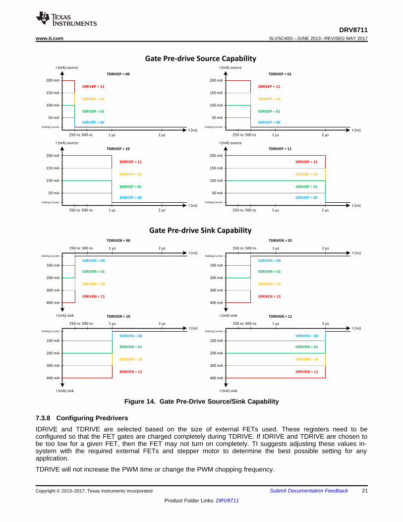
7.3.7 PredriversAn internal charge pump circuit and predrivers inside the DRV8711 directly drive N-channel MOSFETs, whichdrive the motor current.
The peak drive current of the predrivers is adjustable by setting the bits in the DRIVE register. Peak sourcecurrents may be set to 50 mA, 100 mA, 150 mA, or 200 mA. The peak sink current is approximately 2x the peaksource current. Adjusting the peak current will change the output slew rate, which also depends on the FET inputcapacitance and gate charge.
When changing the state of the output, the peak current is applied for a short period of time (tDRIVE), to chargethe gate capacitance. After this time, a weak current source is used to keep the gate at the desired state. Whenselecting the gate drive strength for a given external FET, the selected current must be high enough to fullycharge and discharge the gate during the time when driven at full current, or excessive power will be dissipatedin the FET.
During high-side turnon, the low-side gate is pulled low. This prevents the gate-source capacitance of the low-side FET from inducing turnon.
The predriver circuits include enforcement of a dead time in analog circuitry, which prevents the high-side andlow-side FETs from conducting at the same time. Additional dead time is added with digital delays. This delaycan be selected by setting the DTIME bits in the CTRL register.
Figure 13. Predrivers
t (ns)
I (mA) source
200 mA
150 mA
100 mA
50 mA
Holding Current
250 ns 500 ns 1 µs 2 µs
t (ns)
I (mA) source
200 mA
150 mA
100 mA
50 mA
Holding Current
250 ns 500 ns 1 µs 2 µs
t (ns)
I (mA) source
200 mA
150 mA
100 mA
50 mA
250 ns 500 ns 1 µs 2 µs
t (ns)
I (mA) source
200 mA
150 mA
100 mA
50 mA
Holding Current
250 ns 500 ns 1 µs 2 µs
TDRIVEP = 00 TDRIVEP = 01
TDRIVEP = 10 TDRIVEP = 11
IDRIVEP = 11
IDRIVEP = 10
IDRIVEP = 01
IDRIVEP = 00
IDRIVEP = 11
IDRIVEP = 10
IDRIVEP = 01
IDRIVEP = 00
IDRIVEP = 11
IDRIVEP = 10
IDRIVEP = 01
IDRIVEP = 00
IDRIVEP = 11
IDRIVEP = 10
IDRIVEP = 01
IDRIVEP = 00
250 ns
t (ns)
I (mA) sink
400 mA
300 mA
200 mA
100 mA
Holding Current
250 ns 500 ns 1 µs 2 µs
t (ns)
I (mA) sink
400 mA
300 mA
200 mA
100 mA
Holding Current
250 ns 500 ns 1 µs 2 µs
t (ns)
I (mA) sink
400 mA
300 mA
200 mA
100 mA
500 ns 1 µs 2 µs
t (ns)
I (mA) sink
400 mA
300 mA
200 mA
100 mA
Holding Current
250 ns 500 ns 1 µs 2 µs
TDRIVEN = 00 TDRIVEN = 01
TDRIVEN = 10 TDRIVEN = 11
IDRIVEN = 11
IDRIVEN = 10
IDRIVEN = 01
IDRIVEN = 00
IDRIVEN = 11
IDRIVEN = 10
IDRIVEN = 01
IDRIVEN = 00
IDRIVEN = 11
IDRIVEN = 10
IDRIVEN = 01
IDRIVEN = 00
IDRIVEN = 11
IDRIVEN = 10
IDRIVEN = 01
IDRIVEN = 00
Holding Current
Holding Current
Gate Pre-drive Sink Capability
Gate Pre-drive Source Capability
21
DRV8711www.ti.com SLVSC40G –JUNE 2013–REVISED MAY 2017
Product Folder Links: DRV8711
Submit Documentation FeedbackCopyright © 2013–2017, Texas Instruments Incorporated
Figure 14. Gate Pre-Drive Source/Sink Capability
7.3.8 Configuring PredriversIDRIVE and TDRIVE are selected based on the size of external FETs used. These registers need to beconfigured so that the FET gates are charged completely during TDRIVE. If IDRIVE and TDRIVE are chosen tobe too low for a given FET, then the FET may not turn on completely. TI suggests adjusting these values in-system with the required external FETs and stepper motor to determine the best possible setting for anyapplication.
TDRIVE will not increase the PWM time or change the PWM chopping frequency.
20mA (2 DTIME TBLANK TOFF)Q
4
· · + +<
22
DRV8711SLVSC40G –JUNE 2013–REVISED MAY 2017 www.ti.com
Product Folder Links: DRV8711
Submit Documentation Feedback Copyright © 2013–2017, Texas Instruments Incorporated
In a system with capacitor charge Q and desired rise time RT, IDRIVE and TDRIVE can be initially selectedbased on:
IDRIVE > Q / RT
TDRIVE > 2 × RT
For best results, select the smallest IDRIVE and TDRIVE that meet the above conditions.
Example:
If the gate charge is 15 nC and the desired rise time is 400 ns, then select:
IDRIVEP = 50 mA, IDRIVEN = 100 mA
TDRIVEP = TDRIVEN = 1 µs
7.3.9 External FET SelectionIn a typical setup, the DRV8711 can support external FETs over 50 nC each. However, this capacity can belower or higher based on the device operation. For an accurate calculation of FET driving capacity, use thefollowing equation.
(3)
Example:
If a DTIME is set to 0 (400 ns), TBLANK is set to 0 (1 µs), and TOFF is set to 0 (500 ns), then the DRV8711 willsupport Q < 11.5 nC FETs (this is an absolute worst-case scenario with a PWM frequencyapproximately 430 kHz).
If a DTIME is set to 0 (400 ns), TBLANK is set to 0 (1 µs), and TOFF is set to 0x14 (10 µs), then the DRV8711will support Q < 59 nC FETs (PWM frequency approximately 85 kHz).
If a DTIME is set to 0 (400 ns), TBLANK is set to 0 (1 µs), and TOFF is set to 0x60 (48 µs), then the DRV8711will support Q < 249 nC FETs (PWM frequency approximately 20 kHz).
7.3.10 Stall DetectionThe DRV8711 implements a back EMF monitoring scheme that is capable of detecting a stall during steppermotor motion. This stall detection is intended to be used to get an indication when a motor is run into amechanical stop, or when an increased torque load on the motor causes it to stall.
To determine that a stall has occurred, a drop in motor back EMF is detected. The DRV8711 supports twomethods of this detection: an automatic internal stall detection circuit, or the ability to use an externalmicrocontroller to monitor back EMF.
During a zero-current step, one side of the H-bridge is placed in a high impedance state, and the opposite low-side FET is turned on for a brief duration defined by TORQUE register SMPLTH bit [10:8]. This allows the currentto decay quickly through the low-side FET and the opposite body diode. Which side of the bridge is tri-state andwhich one is driven low depends on the current direction on the previous step. The bridge with the high side thathas been actively PWMed (at the beginning of the PWM cycle during blank time) before entering the zero-currentstep will be held low and the opposite side will be tri-stated.
Back EMF is sampled on the tri-stated output pin at the end of SMPLTH time (TORQUE register bit [10:8]). Theback EMF from the selected pin is divided by 4, 8, 16, or 32, depending on the setting of the VDIV bits in theSTALL register. The voltage is buffered and held on an external capacitor placed on the BEMF pin. The signal onthe BEMF output pin can be further processed by a microcontroller to implement more advanced control and stalldetection algorithms.
The SMPLTH bit [10] is a write-only bit. When read, the bit always reads 0. TI recommends to maintain the valueof the bit locally. When a change in the TORQUE register is desired, the bit can be read locally and added to theother bits to complete the value.
AOUT1
Step
Motor
VM
AOUT2
VM
DAC
8
reference
1.80 V
SDTHR
DAC
SDTHR
BOUT1
VM
BOUT2
VM
bufferBEMF
control
logic
comp
+
-counter
STALLn/
BEMFVn
SDCNT
2
VDIV
2
VDIV
2
VDIV
2
VDIV
2
To
STATUS
register
V5
23
DRV8711www.ti.com SLVSC40G –JUNE 2013–REVISED MAY 2017
Product Folder Links: DRV8711
Submit Documentation FeedbackCopyright © 2013–2017, Texas Instruments Incorporated
Figure 15. Stall Detection
7.3.10.1 Internal Stall DetectionTo use internal stall detection, the EXSTALL bit in the CTRL register is set to 0. In this mode, theSTALLn/BEMFVn output pin is used to signal a valid stall condition.
The time between step inputs must be greater than SMPLTH time for back EMF sampling.
Using internal stall detection, a stall is detected when the sampled back EMF drops below the value set by theSDTHR bits in the STALL register. A programmable counter circuit allows the assertion of the STALLn output tobe delayed until the back EMF has been sampled below the SDTHR value for more than one zero-current step.The counter is programmed by the SDCNT bits in the STALL register, and provides selections of 1, 2, 4, or 8steps.
When the stall is detected (at the end of a SMPLTH interval), the STALLn/BEMFVn pin is driven active low, andthe STD bit and the STDLAT bit in the STATUS register are set. The STALLn/BEMFVn pin will deassert and theSTD bit will automatically clear at the next zero-current step if a stall condition is not detected, while the STDLATbit will remain set until a 0 is written to it. The STDLAT is reset when the STD bit clears after the first zero-crossstep that does not detect a stall condition.
This stall detection scheme is only effective when the motor is stalled while running at or above some minimumspeed. Because it relies on detecting a drop in motor back EMF, the motor must be rotating with sufficient speedto generate a detectable back EMF. During motor start-up, and at very slow step rates, the stall detection is notreliable.
Because back EMF can only be sampled during a zero-current state, stall detection is not possible in full stepmode. During full-step operation, the stall detect circuit is gated off to prevent false signaling of a stall.
The correct setting of the SDTHR bits needs to be determined experimentally. It is dependent on many factors,including the electrical and mechanical characteristics of the load, the peak current setting, and the supplyvoltage.

24
DRV8711SLVSC40G –JUNE 2013–REVISED MAY 2017 www.ti.com
Product Folder Links: DRV8711
Submit Documentation Feedback Copyright © 2013–2017, Texas Instruments Incorporated
7.3.10.2 External Stall DetectionTo use an external microcontroller to manage stall detection, the EXSTALL bit in the CTRL register is set to 1. Inthis mode, the STALLn / BEMFVn output pin is used to signal a valid back EMF measurement is ready. Inaddition, the SDT and SDTLAT bits are also set at this time.
BEMFVn and BEMF are still valid outputs in this mode even if the step time is smaller than SMPLTH time.
When the BEMFVn pin goes active low, it is an indication that a valid back EMF voltage measurement isavailable. This signal could be used, for example, to trigger an interrupt on a microcontroller. The microcontrollercan then sample the voltage present (using an A/D converter) on the BEMF pin.
After sampling the back EMF voltage, the microcontroller writes a 0 to the SDTLAT bit to clear the SDT bit andBEMFVn pin, in preparation for the next back EMF sample. If the SDTLAT bit is not cleared by themicrocontroller, it will automatically be cleared in the next zero-current step.
For either internal or external stall detection, at very high motor speeds when the PWM duty cycle approaches100%, the inductance of the motor and the short duration of each step may cause the time required for currentrecirculation to exceed the step time. In this case, back EMF will not be correctly sampled, and stall detectioncannot function. This condition occurs most at high degrees of micro-stepping, because the zero current steplasts for a shorter duration. It is advisable to run the motor at lower degrees of micro-stepping at higher speedsto allow time for current recirculation if stall detection is needed in this condition.
7.3.11 Protection CircuitsThe DRV8711 is fully protected against undervoltage, overcurrent and overtemperature events.
7.3.11.1 Overcurrent Protection (OCP)Overcurrent is sensed by monitoring the voltage drop across the external FETs. If the voltage across a drivenFET exceeds the value programmed by the OCPTH bits in the DRIVE register for more than the time periodspecified by the OCPDEG bits in the DRIVE register, an OCP event is recognized. When operating in directPWM mode, during an OCP event, the H-bridge experiencing the OCP event is disabled; if operating in indexermode, both H-bridges will be disabled. In addition, the corresponding xOCP bit in the STATUS register is set,and the FAULTn pin is driven low. The H-bridge(s) will remain off, and the xOCP bit will remain set, until it iswritten to 0, or the device is reset.
7.3.11.2 Predriver FaultIn PWM mode, if excessive current is detected on the gate drive outputs (which would be indicative of afailed/shorted output FET or PCB fault), the H-bridge experiencing the fault is disabled, the xPDF bit in theSTATUS register is set, and the FAULTn pin is driven low. The H-bridge will remain off, and the xPDF bit willremain set until it is written to 0 or the device is reset.
When in indexer mode, both H-bridges are disabled, the xPDF bit in the STATUS register is set, and the FAULTnpin is driven low. The H-bridges will remain off, and the xPDF bit will remain set until it is written to 0 or thedevice is reset.
7.3.11.3 Thermal Shutdown (TSD)If the die temperature exceeds safe limits, all FETs in the H-bridge will be disabled, the OTS bit in the STATUSregister will be set, and the FAULTn pin will be driven low. Once the die temperature has fallen to a safe leveloperation will automatically resume and the OTS bit will reset. The FAULTn pin will be released after operationhas resumed.
7.3.11.4 Undervoltage Lockout (UVLO)If at any time the voltage on the VM pin falls below the undervoltage lockout threshold voltage, all FETs in the H-bridge will be disabled, the UVLO bit in the STATUS register will be set, and the FAULTn pin will be driven low.Operation will resume when VM rises above the UVLO threshold. The UVLO bit will remain set until it is writtento 0. The FAULTn pin will be released after operation has resumed.
During any of these fault conditions, the STEP input pin will be ignored.

25
DRV8711www.ti.com SLVSC40G –JUNE 2013–REVISED MAY 2017
Product Folder Links: DRV8711
Submit Documentation FeedbackCopyright © 2013–2017, Texas Instruments Incorporated
7.4 Device Functional Modes
7.4.1 RESET and SLEEPn OperationAn internal power-up reset circuit monitors the voltage applied to the VM pin. If VM falls below the VMundervoltage lockout voltage, the part is reset, as described below for the case of asserting the RESET pin.
If the RESET pin is asserted, all internal logic including the indexer is reset. All registers are returned to theirinitial default conditions. The power stage will be disabled, and all inputs, including STEP and the serial interface,are ignored when RESET is active.
On exiting reset state, some time (approximately 1 mS) needs to pass before the part is fully functional.
Applying an active low input to the SLEEPn input pin will place the device into a low power state. In sleep mode,the motor driver circuitry is disabled, the gate drive regulator and charge pump are disabled, and all analogcircuitry is placed into a low power state. The digital circuitry in the device still operates, so the device registerscan still be accessed via the serial interface.
When SLEEPn is active, the RESET pin does not function. SLEEPn must be exited before RESET will takeeffect. SLEEPn must also be exited to clear the UVLO bit in the status register.
When exiting from sleep mode, some time (approximately 1 mS) needs to pass before applying a STEP input, toallow the internal circuitry to stabilize.
7.4.2 Microstepping Drive CurrentFigure 16 shows examples of stepper motor current in one of the windings. Because these waveforms aredependent on DRV8711 register settings as well as the external FETs, sense resistor, and stepper motor, theyshould only be used as a reference.
Figure 16. Microstepping Drive Current
7.5 Programming
7.5.1 Serial Data FormatThe serial data consists of a 16-bit serial write, with a read/write bit, 3 address bits and 12 data bits. The 3address bits identify one of the registers defined in the register section above. To complete the read or writetransaction, SCS must be set to a logic 0.
To write to a register, data is shifted in after the address as shown in the timing diagram below. The first bit atthe beginning of the access must be logic low for a write operation.

4 0123567891011Address
HexName
TORQUE
CTRL
Name
BLANK
OFF
STALL
DECAY
STATUS
DRIVE
01
00
Address
Hex
03
02
05
04
07
06
4 0123567891011
RW
RW
MODE
DRV8711 REGISTER MAP
SDTHR
RW
RW
RW
RW
RW
RW
RW
ENBL
OTSAOCPBOCP
RDIRRSTEP
UVLO
TORQUE
TOFF
TBLANK
OCPDEG OCPTH
ISGAIN
TDECAYDECMOD
Reserved
Reserved
Reserved
Reserved
DTIME
SDCNT
ABT
Reserved
VDIV
PWMMODE
STDSTDLAT APDFBPDF
TDRIVENTDRIVEPIDRIVENIDRIVEP
EXSTALL
SMPLTH
SCS
SCLK
SDATI
1 2 3 4 5 6 9 11 12 13 614 15 16Note 1
READ A2 A1 A0
SDATO D5 D4 D3
10
D11 D10 D9 D8 D7 D6
7 8
D2 D1 D0
SCS
SCLK
SDATI
1 2 3 4 5 6 7 8 9 10 11 12 13 14 15 16
D3 D2 D1 D0
Note 1
WRT A2 A1 A0 D7 D6 D5 D4D11 D D9 D8 X10
26
DRV8711SLVSC40G –JUNE 2013–REVISED MAY 2017 www.ti.com
Product Folder Links: DRV8711
Submit Documentation Feedback Copyright © 2013–2017, Texas Instruments Incorporated
Programming (continued)
A. Any amount of time may pass between bits, as long as SCS stays active high. This allows two 8-bit writes to be used.
Figure 17. Write Operation
Data may be read from the registers through the SDATO pin. During a read operation, only the address is usedform the SDATI pin; the data bits following are ignored. The first bit at the beginning of the access must be logichigh for a read operation.
(1) Any amount of time may pass between bits, as long as SCS stays active high. This allows two 8-bit writes to be used.
Figure 18. Read Operation
7.6 Register Maps
7.6.1 Control RegistersThe DRV8711 uses internal registers to control the operation of the motor. The registers are programmedthrough a serial SPI communications interface. At power up or reset, the registers will be preloaded with defaultvalues as shown in CTRL Register (Address = 0x00) to STATUS Register (Address = 0x07).
Figure 19 is a map of the DRV8711 registers.
Individual register contents are defined in CTRL Register (Address = 0x00) to STATUS Register (Address =0x07).
Figure 19. DRV8711 Register Map
27
DRV8711www.ti.com SLVSC40G –JUNE 2013–REVISED MAY 2017
Product Folder Links: DRV8711
Submit Documentation FeedbackCopyright © 2013–2017, Texas Instruments Incorporated
Register Maps (continued)7.6.2 CTRL Register (Address = 0x00)
BIT NAME SIZE R/W DEFAULT DESCRIPTION
0 ENBL 1 R/W 0 0: Disable motor1: Enable motor
1 RDIR 1 R/W 0 0: Direction set by DIR pin1: Direction set by inverse of DIR pin
2 RSTEP 1 W 0 0: No action1: Indexer will advance one step; automatically cleared after write
6-3 MODE 4 R/W 0010
0000: Full-step, 71% current0001: Half step0010: 1/4 step0011: 1/8 step0100: 1/16 step0101: 1/32 step0110: 1/64 step0111: 1/128 step1000: 1/256 step1001 – 1111: Reserved
7 EXSTALL 1 R/W 0 0: Internal stall detect1: External stall detect
9-8 ISGAIN 2 R/W 00
ISENSE amplifier gain set00: Gain of 501: Gain of 1010: Gain of 2011: Gain of 40
11-10 DTIME 2 R/W 11
Dead time set00: 400 ns dead time01: 450 ns dead time10: 650 ns dead time11: 850 ns dead time
(1) Bit 10 is a write only bit. When read, bit 10 will always return 0.
7.6.3 TORQUE Register (Address = 0x01)
BIT NAME SIZE R/W DEFAULT DESCRIPTION7-0 TORQUE 8 R/W 0xFF Sets full-scale output current for both H-bridges
10-8 SMPLTH (1) 3 R/W 001
Back EMF sample threshold000: 50 µs001: 100 µs010: 200 µs011: 300 µs100: 400 µs101: 600 µs110: 800 µs111: 1000 µs
11 Reserved 1 - - Reserved
7.6.4 OFF Register (Address = 0x02)
BIT NAME SIZE R/W DEFAULT DESCRIPTION
7-0 TOFF 8 R/W 0x30Sets fixed off time, in increments of 500 ns0x00: 500 ns0xFF: 128 µs
8 PWMMODE 1 R/W 0 0: Use internal indexer1: Bypass indexer, use xINx inputs to control outputs
11-9 Reserved 3 - - Reserved

28
DRV8711SLVSC40G –JUNE 2013–REVISED MAY 2017 www.ti.com
Product Folder Links: DRV8711
Submit Documentation Feedback Copyright © 2013–2017, Texas Instruments Incorporated
7.6.5 BLANK Register (Address = 0x03)
BIT NAME SIZE R/W DEFAULT DESCRIPTION
7-0 TBLANK 8 R/W 0x80
Sets current trip blanking time, in increments of 20 ns0x00: 1 µs…0x32: 1 µs0x33: 1.02 µs…0xFE: 5.10 µs0xFF: 5.12 µsAlso sets minimum on-time of PWM
8 ABT 1 R/W 0 0: Disable adaptive blanking time1: Enable adaptive blanking time
11-9 Reserved 3 - - Reserved
7.6.6 DECAY Register (Address = 0x04)
BIT NAME SIZE R/W DEFAULT DESCRIPTION7-0 TDECAY 8 R/W 0x10 Sets mixed decay transition time, in increments of 500 ns
10-8 DECMOD 3 R/W 001
000: Force slow decay at all times001: Slow decay for increasing current, mixed decay fordecreasing current (indexer mode only)010: Force fast decay at all times011: Use mixed decay at all times100: Slow decay for increasing current, auto mixed decay fordecreasing current (indexer mode only)101: Use auto mixed decay at all times110 – 111: Reserved
11 Reserved 1 - - Reserved
7.6.7 STALL Register (Address = 0x05)
BIT NAME SIZE R/W DEFAULT DESCRIPTION
7-0 SDTHR 8 R/W 0x40 Sets stall detect thresholdThe correct setting needs to be determined experimentally
9-8 SDCNT 2 R/W 00
00: STALLn asserted on first step with back EMF below SDTHR01: STALLn asserted after 2 steps10: STALLn asserted after 4 steps11: STALLn asserted after 8 steps
11-10 VDIV 2 R/W 00
00: Back EMF is divided by 3201: Back EMF is divided by 1610: Back EMF is divided by 811: Back EMF is divided by 4
7.6.8 DRIVE Register (Address = 0x06)
BIT NAME SIZE R/W DEFAULT DESCRIPTION
1-0 OCPTH 2 R/W 01
OCP threshold00: 250 mV01: 500 mV10: 750 mV11: 1000 mV
3-2 OCPDEG 2 R/W 10
OCP deglitch time00: 1 µs01: 2 µs10: 4 µs11: 8 µs
5-4 TDRIVEN 2 R/W 01
Low-side gate drive time00: 250 ns01: 500 ns10: 1 µs11: 2 µs
29
DRV8711www.ti.com SLVSC40G –JUNE 2013–REVISED MAY 2017
Product Folder Links: DRV8711
Submit Documentation FeedbackCopyright © 2013–2017, Texas Instruments Incorporated
BIT NAME SIZE R/W DEFAULT DESCRIPTION
7-6 TDRIVEP 2 R/W 01
High-side gate drive time00: 250 ns01: 500 ns10: 1 µs11: 2 µs
9-8 IDRIVEN 2 R/W 10
Low-side gate drive peak current00: 100 mA peak (sink)01: 200 mA peak (sink)10: 300 mA peak (sink)11: 400 mA peak (sink)
11-10 IDRIVEP 2 R/W 10
High-side gate drive peak current00: 50 mA peak (source)01: 100 mA peak (source)10: 150 mA peak (source)11: 200 mA peak (source)
7.6.9 STATUS Register (Address = 0x07)
BIT NAME SIZE R/W DEFAULT DESCRIPTION
0 OTS 1 R/W 0
0: Normal operation1: Device has entered overtemperature shutdownWrite a 0 to this bit to clear the fault.Operation automatically resumes when the temperature has fallen tosafe levels.
1 AOCP 1 R/W 00: Normal operation1: Channel A overcurrent shutdownWrite a 0 to this bit to clear the fault and resume operation
2 BOCP 1 R/W 00: Normal operation1: Channel B overcurrent shutdownWrite a 0 to this bit to clear the fault and resume operation
3 APDF 1 R/W 00: Normal operation1: Channel A predriver faultWrite a 0 to this bit to clear the fault and resume operation.
4 BPDF 1 R/W 00: Normal operation1: Channel B predriver faultWrite a 0 to this bit to clear the fault and resume operation
5 UVLO 1 R/W 0
0: Normal operation1: Undervoltage lockoutWrite a 0 to this bit to clear the fault. The UVLO bit cannot be clearedin sleep mode. Operation automatically resumes when VM hasincreased above VUVLO
6 STD 1 R 0 0: Normal operation1: Stall detected
7 STDLAT 1 R/W 00: Normal operation1: Latched stall detectWrite a 0 to this bit to clear the fault and resume operation
11-8 Reserved 4 - - Reserved
30
DRV8711SLVSC40G –JUNE 2013–REVISED MAY 2017 www.ti.com
Product Folder Links: DRV8711
Submit Documentation Feedback Copyright © 2013–2017, Texas Instruments Incorporated
8 Application and Implementation
NOTEInformation in the following applications sections is not part of the TI componentspecification, and TI does not warrant its accuracy or completeness. TI’s customers areresponsible for determining suitability of components for their purposes. Customers shouldvalidate and test their design implementation to confirm system functionality.
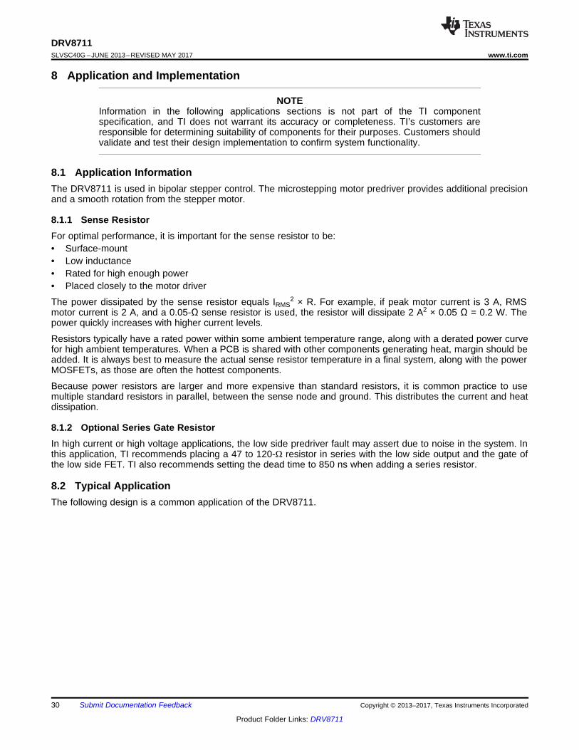
8.1 Application InformationThe DRV8711 is used in bipolar stepper control. The microstepping motor predriver provides additional precisionand a smooth rotation from the stepper motor.
8.1.1 Sense ResistorFor optimal performance, it is important for the sense resistor to be:• Surface-mount• Low inductance• Rated for high enough power• Placed closely to the motor driver
The power dissipated by the sense resistor equals IRMS2 × R. For example, if peak motor current is 3 A, RMS
motor current is 2 A, and a 0.05-Ω sense resistor is used, the resistor will dissipate 2 A2 × 0.05 Ω = 0.2 W. Thepower quickly increases with higher current levels.
Resistors typically have a rated power within some ambient temperature range, along with a derated power curvefor high ambient temperatures. When a PCB is shared with other components generating heat, margin should beadded. It is always best to measure the actual sense resistor temperature in a final system, along with the powerMOSFETs, as those are often the hottest components.
Because power resistors are larger and more expensive than standard resistors, it is common practice to usemultiple standard resistors in parallel, between the sense node and ground. This distributes the current and heatdissipation.
8.1.2 Optional Series Gate ResistorIn high current or high voltage applications, the low side predriver fault may assert due to noise in the system. Inthis application, TI recommends placing a 47 to 120-Ω resistor in series with the low side output and the gate ofthe low side FET. TI also recommends setting the dead time to 850 ns when adding a series resistor.
8.2 Typical ApplicationThe following design is a common application of the DRV8711.
PPAD
GND
AOUT1
A1HS
A1LS
AISENP
AISENN
A2LS
A2HS
AOUT2
GND
BOUT1
B1HS
B1LS
BISENP
BISENN
B2LS
B2HS
BOUT2
BEMF
VINT
SLEEPn
RESET
STEP / AIN1
DIR / AIN2
BIN1
BIN2
SCLK
SDATI
SCS
SDATO
FAULTn
STALLn / BEMFVn
CP2
VCP
VM
GND
V5
CP1
DRV8711
0.1 uF
1 uF0.01 uF
1 nF
100 uF
VM
+
TYPICAL APPLICATION
StepMotor
VM
VM
0.1 uF
1 uF
VM
VM
MCUWith Optional
ADC (for BEMF)
50 P
50 P
(1)
(1)
(1)
(1)
(1) Optional series resistor
31
DRV8711www.ti.com SLVSC40G –JUNE 2013–REVISED MAY 2017
Product Folder Links: DRV8711
Submit Documentation FeedbackCopyright © 2013–2017, Texas Instruments Incorporated
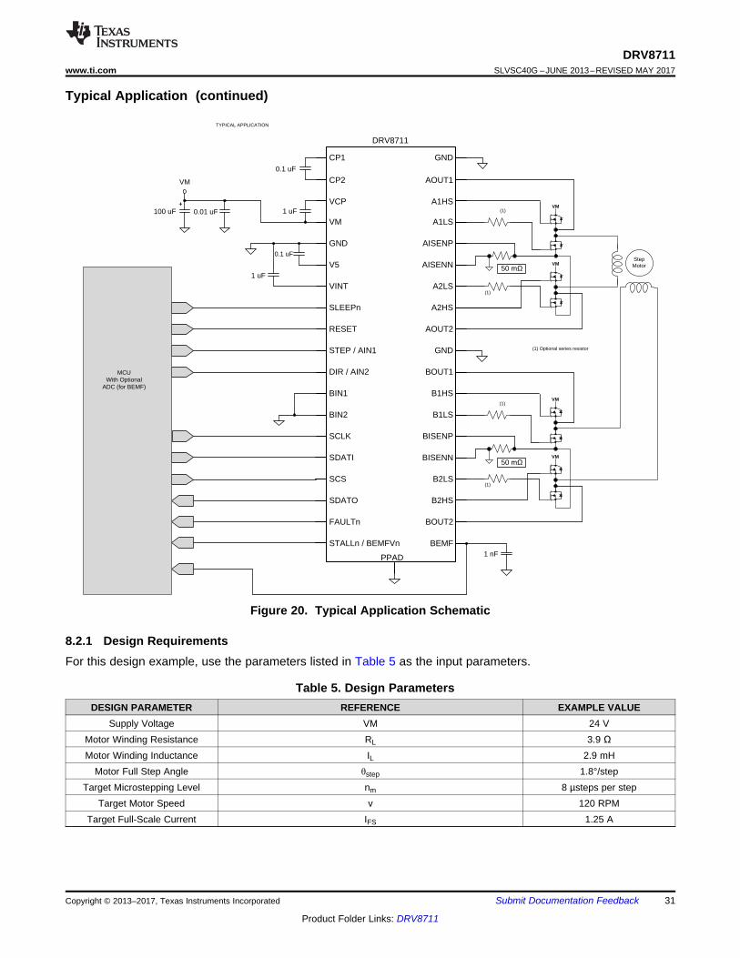
Typical Application (continued)
Figure 20. Typical Application Schematic
8.2.1 Design RequirementsFor this design example, use the parameters listed in Table 5 as the input parameters.
Table 5. Design ParametersDESIGN PARAMETER REFERENCE EXAMPLE VALUE
Supply Voltage VM 24 VMotor Winding Resistance RL 3.9 ΩMotor Winding Inductance IL 2.9 mH
Motor Full Step Angle θstep 1.8°/stepTarget Microstepping Level nm 8 µsteps per step
Target Motor Speed v 120 RPMTarget Full-Scale Current IFS 1.25 A

( )( )
( )FS
SENSE
2.75 V TORQUEI A =
256 ISGAIN R´ ´ W
´
( )step
rotations ° µsteps120 360 8
minute rotation stepf µsteps/second =
seconds °60 1.8
minute step
æ öæ ö æ ö´ ´ ç ÷ç ÷ ç ÷
è ø è ø è øæ öæ ö
´ ç ÷ç ÷è ø è ø
( )m
step
step
rotations ° µstepsv × 360 × n
minute rotation stepf µsteps/second =
seconds °60 × θ
minute step
æ öæ ö æ öç ÷ç ÷ ç ÷
è ø è ø è øæ öæ öç ÷ç ÷
è ø è ø
32
DRV8711SLVSC40G –JUNE 2013–REVISED MAY 2017 www.ti.com
Product Folder Links: DRV8711
Submit Documentation Feedback Copyright © 2013–2017, Texas Instruments Incorporated
8.2.2 Detailed Design Procedure
8.2.2.1 Stepper Motor SpeedThe first step in configuring the DRV8711 requires the desired motor speed and microstepping level. If the targetapplication requires a constant speed, then a square wave with frequency ƒstep must be applied to the STEP pin.
If the target motor start-up speed is too high, the motor will not spin. Make sure that the motor can support thetarget speed or implement an acceleration profile to bring the motor up to speed.
For a desired motor speed (V), microstepping level (nm), and motor full step angle (θstep),
(4)
(5)
θstep can be found in the stepper motor data sheet or written on the motor itself.
For the DRV8711, the microstepping level is set by the MODE bits in the CTRL register. Higher microsteppingwill mean a smoother motor motion and less audible noise, but will increase switching losses and require ahigher fstep to achieve the same motor speed.
8.2.2.2 Current RegulationIn a stepper motor, the set full-scale current (IFS) is the maximum current driven through either winding. For theDRV8711, this quantity will depend on the analog voltage, the programmed torque and gain values, and thesense resistor value (RSENSE). During stepping, IFS defines the current chopping threshold (ITRIP) for themaximum current step. The gain of DRV8711 is set for 5 V/V.
(6)
To achieve IFS = 1.25 A with RSENSE of 0.2 Ω with a gain of 5, TORQUE should be set to 116(dec).
8.2.2.3 Decay ModesThe DRV8711 supports three different decay modes: slow decay, fast decay, and mixed decay. The DRV8711also supports automatic mixed decay mode, which minimizes current ripple. The current through the motorwindings is regulated using programmable settings for blanking, decay and off time. This means that after anydrive phase, when a motor winding current has hit the current chopping threshold (ITRIP), the DRV8711 will placethe winding in the programmed decay modes until the cycle has expired. Afterward, a new drive phase starts.
The blanking time TBLANK defines the minimum drive time for the current chopping. ITRIP is ignored during TBLANK,so the winding current may overshoot the trip level.

33
DRV8711www.ti.com SLVSC40G –JUNE 2013–REVISED MAY 2017
Product Folder Links: DRV8711
Submit Documentation FeedbackCopyright © 2013–2017, Texas Instruments Incorporated
8.2.3 Application Curves
Figure 21. 1/32 Microstepping Drive Current Figure 22. 1/64 Microstepping Drive Current

Local Bulk Capacitor
Parasitic WireInductance
+±
Motor Driver
Power Supply Motor Drive System
VM
GND
+
IC Bypass Capacitor
34
DRV8711SLVSC40G –JUNE 2013–REVISED MAY 2017 www.ti.com
Product Folder Links: DRV8711
Submit Documentation Feedback Copyright © 2013–2017, Texas Instruments Incorporated
9 Power Supply Recommendations
9.1 Bulk CapacitanceHaving an appropriate local bulk capacitance is an important factor in motor drive system design. It is generallybeneficial to have more bulk capacitance, while the disadvantages are increased cost and physical size.
The amount of local capacitance needed depends on a variety of factors, including:• The highest current required by the motor system• The power supply’s capacitance and ability to source current• The amount of parasitic inductance between the power supply and motor system• The acceptable voltage ripple• The type of motor used (Brushed DC, Brushless DC, Stepper)• The motor braking method
The inductance between the power supply and the motor drive system limits the rate current can change fromthe power supply. If the local bulk capacitance is too small, the system responds to excessive current demandsor dumps from the motor with a change in voltage. When adequate bulk capacitance is used, the motor voltageremains stable and high current can be quickly supplied.
The data sheet generally provides a recommended value, but system-level testing is required to determine theappropriate sized bulk capacitor.
Figure 23. Example Setup of Motor Drive System With External Power Supply
The voltage rating for bulk capacitors should be higher than the operating voltage, to provide margin for caseswhen the motor transfers energy to the supply.

35
DRV8711www.ti.com SLVSC40G –JUNE 2013–REVISED MAY 2017
Product Folder Links: DRV8711
Submit Documentation FeedbackCopyright © 2013–2017, Texas Instruments Incorporated
10 Layout
10.1 Layout GuidelinesThe VM pin should be bypassed to GND using low-ESR ceramic bypass capacitors with a recommended valueof 0.01-μF rated for VM. This capacitor should be placed as close to the VM pin as possible with a thick trace orground plane connection to the device GND pin. The VM pin must be bypassed to ground using an appropriatebulk capacitor. This component may be an electrolytic and should be located close to the DRV8711.
A low-ESR ceramic capacitor must be placed in between the VM and VCP pins. TI recommends a value of 1 μFrated for 16 V. Place this component as close to the pins as possible.
A low-ESR ceramic capacitor must be placed in between the CP1 and CP2 pins. TI recommends a value of 0.1μF rated for VM. Place this component as close to the pins as possible.
Bypass VINT to ground with a 1-μF ceramic capacitor rated 6.3 V. Place this bypass capacitor as close to the pinas possible.
Bypass V5 to ground with a 1-μF ceramic capacitor rated 10 V. Place this bypass capacitor as close to the pin aspossible.

1 µF
0. 1 µFCP1 GND
CP2
VCP
VM
GND
V5
VINT
SLEEPn
RESET
STEP / AIN1
DIR / AIN2
BIN1
AOUT1
A1HS
A1LS
AISENP
AISENN
A2LS
A2HS
AOUT2
GND
BOUT1
B1HS
BIN2
SCLK
B1LS
BISENP
0. 01 µF+
3. 3 k
SDATI
SCS
SDATO
FAULTn
STALLn / BEMFVn
BISENN
B2 LS
B2HS
BOUT2
BEMF
0. 1 µF1 µF
1 µF
Optional 3. 3 k
Logic High
36
DRV8711SLVSC40G –JUNE 2013–REVISED MAY 2017 www.ti.com
Product Folder Links: DRV8711
Submit Documentation Feedback Copyright © 2013–2017, Texas Instruments Incorporated
10.2 Layout Example
Figure 24. Recommended Layout Example

37
DRV8711www.ti.com SLVSC40G –JUNE 2013–REVISED MAY 2017
Product Folder Links: DRV8711
Submit Documentation FeedbackCopyright © 2013–2017, Texas Instruments Incorporated
11 Device and Documentation Support
11.1 Documentation Support
11.1.1 Related DocumentationFor related documentation see the following:• DRV8711 Decay Mode Setting Optimization• DRV8711 Quick Spin and Tuning Guide• PowerPAD™ Thermally Enhanced Package• PowerPAD™ Made Easy
11.2 Receiving Notification of Documentation UpdatesTo receive notification of documentation updates, navigate to the device product folder on ti.com. In the upperright corner, click on Alert me to register and receive a weekly digest of any product information that haschanged. For change details, review the revision history included in any revised document.
11.3 Community ResourcesThe following links connect to TI community resources. Linked contents are provided "AS IS" by the respectivecontributors. They do not constitute TI specifications and do not necessarily reflect TI's views; see TI's Terms ofUse.
TI E2E™ Online Community TI's Engineer-to-Engineer (E2E) Community. Created to foster collaborationamong engineers. At e2e.ti.com, you can ask questions, share knowledge, explore ideas and helpsolve problems with fellow engineers.
Design Support TI's Design Support Quickly find helpful E2E forums along with design support tools andcontact information for technical support.
11.4 TrademarksPowerPAD, E2E are trademarks of Texas Instruments.All other trademarks are the property of their respective owners.
11.5 Electrostatic Discharge CautionThese devices have limited built-in ESD protection. The leads should be shorted together or the device placed in conductive foamduring storage or handling to prevent electrostatic damage to the MOS gates.
11.6 GlossarySLYZ022 — TI Glossary.
This glossary lists and explains terms, acronyms, and definitions.
12 Mechanical, Packaging, and Orderable InformationThe following pages include mechanical, packaging, and orderable information. This information is the mostcurrent data available for the designated devices. This data is subject to change without notice and revision ofthis document. For browser-based versions of this data sheet, refer to the left-hand navigation.
PACKAGE OPTION ADDENDUM
www.ti.com 9-May-2017
Addendum-Page 1
PACKAGING INFORMATION
Orderable Device Status(1)
Package Type PackageDrawing
Pins PackageQty
Eco Plan(2)
Lead/Ball Finish(6)
MSL Peak Temp(3)
Op Temp (°C) Device Marking(4/5)
Samples
DRV8711DCP ACTIVE HTSSOP DCP 38 50 Green (RoHS& no Sb/Br)
CU NIPDAU Level-2-260C-1 YEAR -40 to 85 DRV8711
DRV8711DCPR ACTIVE HTSSOP DCP 38 2000 Green (RoHS& no Sb/Br)
CU NIPDAU Level-2-260C-1 YEAR -40 to 85 DRV8711
(1) The marketing status values are defined as follows:ACTIVE: Product device recommended for new designs.LIFEBUY: TI has announced that the device will be discontinued, and a lifetime-buy period is in effect.NRND: Not recommended for new designs. Device is in production to support existing customers, but TI does not recommend using this part in a new design.PREVIEW: Device has been announced but is not in production. Samples may or may not be available.OBSOLETE: TI has discontinued the production of the device.
(2) RoHS: TI defines "RoHS" to mean semiconductor products that are compliant with the current EU RoHS requirements for all 10 RoHS substances, including the requirement that RoHS substancedo not exceed 0.1% by weight in homogeneous materials. Where designed to be soldered at high temperatures, "RoHS" products are suitable for use in specified lead-free processes. TI mayreference these types of products as "Pb-Free".RoHS Exempt: TI defines "RoHS Exempt" to mean products that contain lead but are compliant with EU RoHS pursuant to a specific EU RoHS exemption.Green: TI defines "Green" to mean the content of Chlorine (Cl) and Bromine (Br) based flame retardants meet JS709B low halogen requirements of <=1000ppm threshold. Antimony trioxide basedflame retardants must also meet the <=1000ppm threshold requirement.
(3) MSL, Peak Temp. - The Moisture Sensitivity Level rating according to the JEDEC industry standard classifications, and peak solder temperature.
(4) There may be additional marking, which relates to the logo, the lot trace code information, or the environmental category on the device.
(5) Multiple Device Markings will be inside parentheses. Only one Device Marking contained in parentheses and separated by a "~" will appear on a device. If a line is indented then it is a continuationof the previous line and the two combined represent the entire Device Marking for that device.
(6) Lead/Ball Finish - Orderable Devices may have multiple material finish options. Finish options are separated by a vertical ruled line. Lead/Ball Finish values may wrap to two lines if the finishvalue exceeds the maximum column width.
Important Information and Disclaimer:The information provided on this page represents TI's knowledge and belief as of the date that it is provided. TI bases its knowledge and belief on informationprovided by third parties, and makes no representation or warranty as to the accuracy of such information. Efforts are underway to better integrate information from third parties. TI has taken andcontinues to take reasonable steps to provide representative and accurate information but may not have conducted destructive testing or chemical analysis on incoming materials and chemicals.TI and TI suppliers consider certain information to be proprietary, and thus CAS numbers and other limited information may not be available for release.
In no event shall TI's liability arising out of such information exceed the total purchase price of the TI part(s) at issue in this document sold by TI to Customer on an annual basis.

PACKAGE OPTION ADDENDUM
www.ti.com 9-May-2017
Addendum-Page 2

TAPE AND REEL INFORMATION
*All dimensions are nominal
Device PackageType
PackageDrawing
Pins SPQ ReelDiameter
(mm)
ReelWidth
W1 (mm)
A0(mm)
B0(mm)
K0(mm)
P1(mm)
W(mm)
Pin1Quadrant
DRV8711DCPR HTSSOP DCP 38 2000 330.0 16.4 6.9 10.2 1.8 12.0 16.0 Q1
PACKAGE MATERIALS INFORMATION
www.ti.com 9-May-2017
Pack Materials-Page 1

*All dimensions are nominal
Device Package Type Package Drawing Pins SPQ Length (mm) Width (mm) Height (mm)
DRV8711DCPR HTSSOP DCP 38 2000 367.0 367.0 38.0
PACKAGE MATERIALS INFORMATION
www.ti.com 9-May-2017
Pack Materials-Page 2

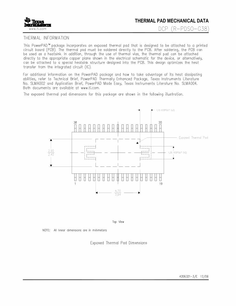

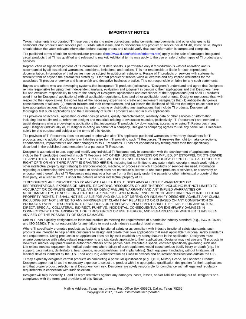
IMPORTANT NOTICE
Texas Instruments Incorporated (TI) reserves the right to make corrections, enhancements, improvements and other changes to itssemiconductor products and services per JESD46, latest issue, and to discontinue any product or service per JESD48, latest issue. Buyersshould obtain the latest relevant information before placing orders and should verify that such information is current and complete.TI’s published terms of sale for semiconductor products (http://www.ti.com/sc/docs/stdterms.htm) apply to the sale of packaged integratedcircuit products that TI has qualified and released to market. Additional terms may apply to the use or sale of other types of TI products andservices.Reproduction of significant portions of TI information in TI data sheets is permissible only if reproduction is without alteration and isaccompanied by all associated warranties, conditions, limitations, and notices. TI is not responsible or liable for such reproduceddocumentation. Information of third parties may be subject to additional restrictions. Resale of TI products or services with statementsdifferent from or beyond the parameters stated by TI for that product or service voids all express and any implied warranties for theassociated TI product or service and is an unfair and deceptive business practice. TI is not responsible or liable for any such statements.Buyers and others who are developing systems that incorporate TI products (collectively, “Designers”) understand and agree that Designersremain responsible for using their independent analysis, evaluation and judgment in designing their applications and that Designers havefull and exclusive responsibility to assure the safety of Designers' applications and compliance of their applications (and of all TI productsused in or for Designers’ applications) with all applicable regulations, laws and other applicable requirements. Designer represents that, withrespect to their applications, Designer has all the necessary expertise to create and implement safeguards that (1) anticipate dangerousconsequences of failures, (2) monitor failures and their consequences, and (3) lessen the likelihood of failures that might cause harm andtake appropriate actions. Designer agrees that prior to using or distributing any applications that include TI products, Designer willthoroughly test such applications and the functionality of such TI products as used in such applications.TI’s provision of technical, application or other design advice, quality characterization, reliability data or other services or information,including, but not limited to, reference designs and materials relating to evaluation modules, (collectively, “TI Resources”) are intended toassist designers who are developing applications that incorporate TI products; by downloading, accessing or using TI Resources in anyway, Designer (individually or, if Designer is acting on behalf of a company, Designer’s company) agrees to use any particular TI Resourcesolely for this purpose and subject to the terms of this Notice.TI’s provision of TI Resources does not expand or otherwise alter TI’s applicable published warranties or warranty disclaimers for TIproducts, and no additional obligations or liabilities arise from TI providing such TI Resources. TI reserves the right to make corrections,enhancements, improvements and other changes to its TI Resources. TI has not conducted any testing other than that specificallydescribed in the published documentation for a particular TI Resource.Designer is authorized to use, copy and modify any individual TI Resource only in connection with the development of applications thatinclude the TI product(s) identified in such TI Resource. NO OTHER LICENSE, EXPRESS OR IMPLIED, BY ESTOPPEL OR OTHERWISETO ANY OTHER TI INTELLECTUAL PROPERTY RIGHT, AND NO LICENSE TO ANY TECHNOLOGY OR INTELLECTUAL PROPERTYRIGHT OF TI OR ANY THIRD PARTY IS GRANTED HEREIN, including but not limited to any patent right, copyright, mask work right, orother intellectual property right relating to any combination, machine, or process in which TI products or services are used. Informationregarding or referencing third-party products or services does not constitute a license to use such products or services, or a warranty orendorsement thereof. Use of TI Resources may require a license from a third party under the patents or other intellectual property of thethird party, or a license from TI under the patents or other intellectual property of TI.TI RESOURCES ARE PROVIDED “AS IS” AND WITH ALL FAULTS. TI DISCLAIMS ALL OTHER WARRANTIES ORREPRESENTATIONS, EXPRESS OR IMPLIED, REGARDING RESOURCES OR USE THEREOF, INCLUDING BUT NOT LIMITED TOACCURACY OR COMPLETENESS, TITLE, ANY EPIDEMIC FAILURE WARRANTY AND ANY IMPLIED WARRANTIES OFMERCHANTABILITY, FITNESS FOR A PARTICULAR PURPOSE, AND NON-INFRINGEMENT OF ANY THIRD PARTY INTELLECTUALPROPERTY RIGHTS. TI SHALL NOT BE LIABLE FOR AND SHALL NOT DEFEND OR INDEMNIFY DESIGNER AGAINST ANY CLAIM,INCLUDING BUT NOT LIMITED TO ANY INFRINGEMENT CLAIM THAT RELATES TO OR IS BASED ON ANY COMBINATION OFPRODUCTS EVEN IF DESCRIBED IN TI RESOURCES OR OTHERWISE. IN NO EVENT SHALL TI BE LIABLE FOR ANY ACTUAL,DIRECT, SPECIAL, COLLATERAL, INDIRECT, PUNITIVE, INCIDENTAL, CONSEQUENTIAL OR EXEMPLARY DAMAGES INCONNECTION WITH OR ARISING OUT OF TI RESOURCES OR USE THEREOF, AND REGARDLESS OF WHETHER TI HAS BEENADVISED OF THE POSSIBILITY OF SUCH DAMAGES.Unless TI has explicitly designated an individual product as meeting the requirements of a particular industry standard (e.g., ISO/TS 16949and ISO 26262), TI is not responsible for any failure to meet such industry standard requirements.Where TI specifically promotes products as facilitating functional safety or as compliant with industry functional safety standards, suchproducts are intended to help enable customers to design and create their own applications that meet applicable functional safety standardsand requirements. Using products in an application does not by itself establish any safety features in the application. Designers mustensure compliance with safety-related requirements and standards applicable to their applications. Designer may not use any TI products inlife-critical medical equipment unless authorized officers of the parties have executed a special contract specifically governing such use.Life-critical medical equipment is medical equipment where failure of such equipment would cause serious bodily injury or death (e.g., lifesupport, pacemakers, defibrillators, heart pumps, neurostimulators, and implantables). Such equipment includes, without limitation, allmedical devices identified by the U.S. Food and Drug Administration as Class III devices and equivalent classifications outside the U.S.TI may expressly designate certain products as completing a particular qualification (e.g., Q100, Military Grade, or Enhanced Product).Designers agree that it has the necessary expertise to select the product with the appropriate qualification designation for their applicationsand that proper product selection is at Designers’ own risk. Designers are solely responsible for compliance with all legal and regulatoryrequirements in connection with such selection.Designer will fully indemnify TI and its representatives against any damages, costs, losses, and/or liabilities arising out of Designer’s non-compliance with the terms and provisions of this Notice.
Mailing Address: Texas Instruments, Post Office Box 655303, Dallas, Texas 75265Copyright © 2017, Texas Instruments Incorporated