High-Voltage Stepper Reference Design Using DRV8711 (Rev. A)

Product
Folder
Sample &Buy
Technical
Documents
Tools &
Software
Support &Community
DRV8711
www.ti.com SLVSC40 –JUNE 2013
STEPPER MOTOR CONTROLLER IC1FEATURES2• Pulse Width Modulation (PWM) Microstepping • Protection and Diagnostic Features
Motor Driver – Overcurrent Protection (OCP)– Built-In 1/256-Step Microstepping Indexer – Overtemperature Shutdown (OTS)– Drives External N-Channel MOSFETs – Undervoltage Lockout (UVLO)– Optional STEP/DIR Pins – Individual Fault Condition Indication Bits– Optional PWM Control Interface for DC – Fault Condition Indication Pin
Motors• Flexible Decay Modes, Including Automatic APPLICATIONS
Mixed Decay Mode • Office Automation Machines• Stall Detection With Optional BEMF Output • Factory Automation• Highly cConfigurable Va SPI Serial Interface • Textile Machines• Internal Reference and Torque DAC • Robotics• 8-V to 52-V Operating Supply Voltage Range• Scalable Output Current• Thermally Enhanced Surface Mount Package• 5-V Regulator Capable of 10-mA Load
DESCRIPTIONThe DRV8711 is a stepper motor controller that uses external N-channel MOSFETs to drive a bipolar steppermotor or two brushed DC motors. A microstepping indexer is integrated, which is capable of step modes from fullstep to 1/256-step.
An ultra-smooth motion profile can be achieved using adaptive blanking time and various current decay modes,including an auto-mixed decay mode. Motor stall is reported with an optional back-EMF output.
A simple step/direction or PWM interface allows easy interfacing to controller circuits. A SPI serial interface isused to program the device operation. Output current (torque), step mode, decay mode, and stall detectionfunctions are all programmable via a SPI serial interface.
Internal shutdown functions are provided for over current protection, short circuit protection, under voltagelockout and overtemperature. Fault conditions are indicated via a FAULTn pin, and each fault condition isreported via a dedicated bit through SPI.
The DRV8811 is packaged in a PowerPAD™ 38-pin HTSSOP package with thermal pad (Eco-friendly: RoHSand no Sb/Br).
ORDERING INFORMATION (1)
TA PACKAGE (2) ORDERABLE PART NUMBER TOP-SIDE MARKING
Reel of 2000 DRV8711DCPR–40°C to 85°C PowerPAD™ (HTSSOP) – PWP DRV8711
Tube of 40 DRV8711DCP
(1) For the most current package and ordering information, see the Package Option Addendum at the end of this document, or see the TIweb site at www.ti.com.
(2) Package drawings, thermal data, and symbolization are available at www.ti.com/packaging.
1
Please be aware that an important notice concerning availability, standard warranty, and use in critical applications ofTexas Instruments semiconductor products and disclaimers thereto appears at the end of this data sheet.
2PowerPAD is a trademark of Texas Instruments.
PRODUCTION DATA information is current as of publication date. Copyright © 2013, Texas Instruments IncorporatedProducts conform to specifications per the terms of the TexasInstruments standard warranty. Production processing does notnecessarily include testing of all parameters.

Over-
Temp
AOUT1
GND
RESET
Gate
Drive
&
OCP
Step
Motor
SCS
SCLK
VM
VM
SDATO
SDATI
SLEEPn
100 Fµ
+
0.01 Fµ
VM
PWM
logic
FAULTn
VINT
5V OUT
1 Fµ
CP1CP2 VCP
HS Gate DriveCharge
Pump
UVLO
PUCSTEP/AIN1
A1HSVM
A1LS
AOUT2
A2HSVM
A2LS
BOUT1
B1HSVM
B1LS
BOUT2
B2HSVM
B2LS
Gate
Drive
&
OCP
Gate
Drive
&
OCP
Gate
Drive
&
OCP
BISENP
ISEN
amp
+
-
AISENP
Comp
+
-
PWM
logic
STALLn / BEMFVn
DIR/AIN2
Reference
Stall detect BEMF
SIN
DAC
SIN
DAC
+
-
Comp
+
-ISEN
amp
+
-
Comp
+
-
+
-
Comp
+
-
AISENN
BISENN
BIN1
BIN2
0.1 Fµ1 Fµ
Regs
V5
VM
1nF
0.1 Fµ
X
X
Torque
DAC
Torque
DAC
Logic
DCM
DCM
DRV8711
SLVSC40 –JUNE 2013 www.ti.com
FUNCTIONAL BLOCK DIAGRAM
2 Submit Documentation Feedback Copyright © 2013, Texas Instruments Incorporated
Product Folder Links: DRV8711
DRV8711
www.ti.com SLVSC40 –JUNE 2013
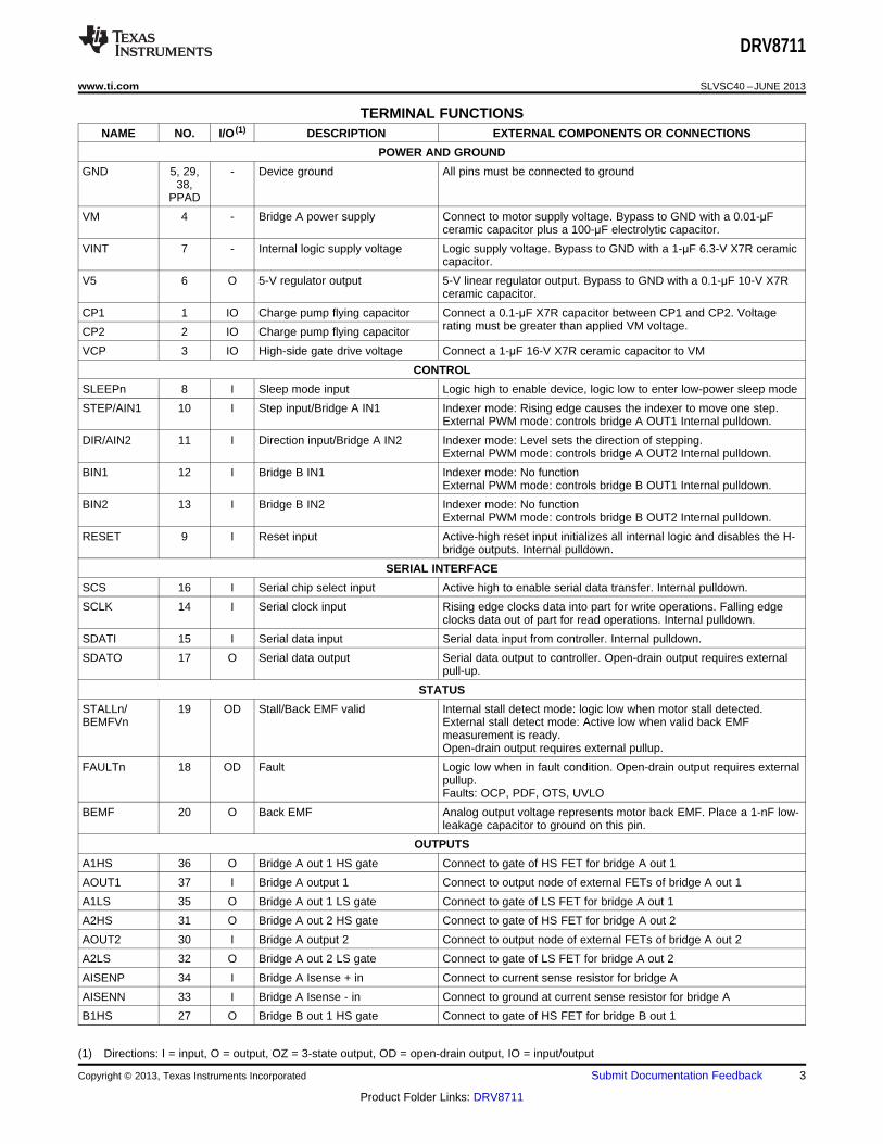
TERMINAL FUNCTIONSNAME NO. I/O (1) DESCRIPTION EXTERNAL COMPONENTS OR CONNECTIONS
POWER AND GROUND
GND 5, 29, - Device ground All pins must be connected to ground38,
PPAD
VM 4 - Bridge A power supply Connect to motor supply voltage. Bypass to GND with a 0.01-μFceramic capacitor plus a 100-μF electrolytic capacitor.
VINT 7 - Internal logic supply voltage Logic supply voltage. Bypass to GND with a 1-μF 6.3-V X7R ceramiccapacitor.
V5 6 O 5-V regulator output 5-V linear regulator output. Bypass to GND with a 0.1-μF 10-V X7Rceramic capacitor.
CP1 1 IO Charge pump flying capacitor Connect a 0.1-μF X7R capacitor between CP1 and CP2. Voltagerating must be greater than applied VM voltage.CP2 2 IO Charge pump flying capacitor
VCP 3 IO High-side gate drive voltage Connect a 1-μF 16-V X7R ceramic capacitor to VM
CONTROL
SLEEPn 8 I Sleep mode input Logic high to enable device, logic low to enter low-power sleep mode
STEP/AIN1 10 I Step input/Bridge A IN1 Indexer mode: Rising edge causes the indexer to move one step.External PWM mode: controls bridge A OUT1 Internal pulldown.
DIR/AIN2 11 I Direction input/Bridge A IN2 Indexer mode: Level sets the direction of stepping.External PWM mode: controls bridge A OUT2 Internal pulldown.
BIN1 12 I Bridge B IN1 Indexer mode: No functionExternal PWM mode: controls bridge B OUT1 Internal pulldown.
BIN2 13 I Bridge B IN2 Indexer mode: No functionExternal PWM mode: controls bridge B OUT2 Internal pulldown.
RESET 9 I Reset input Active-high reset input initializes all internal logic and disables the H-bridge outputs. Internal pulldown.
SERIAL INTERFACE
SCS 16 I Serial chip select input Active high to enable serial data transfer. Internal pulldown.
SCLK 14 I Serial clock input Rising edge clocks data into part for write operations. Falling edgeclocks data out of part for read operations. Internal pulldown.
SDATI 15 I Serial data input Serial data input from controller. Internal pulldown.
SDATO 17 O Serial data output Serial data output to controller. Open-drain output requires externalpull-up.
STATUS
STALLn/ 19 OD Stall/Back EMF valid Internal stall detect mode: logic low when motor stall detected.BEMFVn External stall detect mode: Active low when valid back EMF
measurement is ready.Open-drain output requires external pullup.
FAULTn 18 OD Fault Logic low when in fault condition. Open-drain output requires externalpullup.Faults: OCP, PDF, OTS, UVLO
BEMF 20 O Back EMF Analog output voltage represents motor back EMF. Place a 1-nF low-leakage capacitor to ground on this pin.
OUTPUTS
A1HS 36 O Bridge A out 1 HS gate Connect to gate of HS FET for bridge A out 1
AOUT1 37 I Bridge A output 1 Connect to output node of external FETs of bridge A out 1
A1LS 35 O Bridge A out 1 LS gate Connect to gate of LS FET for bridge A out 1
A2HS 31 O Bridge A out 2 HS gate Connect to gate of HS FET for bridge A out 2
AOUT2 30 I Bridge A output 2 Connect to output node of external FETs of bridge A out 2
A2LS 32 O Bridge A out 2 LS gate Connect to gate of LS FET for bridge A out 2
AISENP 34 I Bridge A Isense + in Connect to current sense resistor for bridge A
AISENN 33 I Bridge A Isense - in Connect to ground at current sense resistor for bridge A
B1HS 27 O Bridge B out 1 HS gate Connect to gate of HS FET for bridge B out 1
(1) Directions: I = input, O = output, OZ = 3-state output, OD = open-drain output, IO = input/output
Copyright © 2013, Texas Instruments Incorporated Submit Documentation Feedback 3
Product Folder Links: DRV8711

1
2
3
4
5
6
7
8
9
10
11
12
13
14 25
26
27
28
29
38
37
36
35
34
33
32
31
30
CP1
15
16
17
18
19 20
21
22
23
24
CP2VCP
VMGND
V5
SLEEPnRESET
VINT
STEP / AIN1
BIN2SCLK
SDATI
SDATOFAULTn
STALLn / BEMFVn BEMF
GNDAOUT1A1HSA1LSAISENPAISENNA2LSA2HSAOUT2GNDBOUT1B1HSB1LSBISENPBISENNB2LSB2HSBOUT2
GND
(PPAD)DIR / AIN2BIN1
SCS
DRV8711
SLVSC40 –JUNE 2013 www.ti.com
TERMINAL FUNCTIONS (continued)
NAME NO. I/O (1) DESCRIPTION EXTERNAL COMPONENTS OR CONNECTIONS
BOUT1 28 I Bridge B output 1 Connect to output node of external FETs of bridge B out 1
B1LS 26 O Bridge B out 1 LS gate Connect to gate of LS FET for bridge B out 1
B2HS 22 O Bridge B out 2 HS gate Connect to gate of HS FET for bridge B out 2
BOUT2 21 I Bridge B output 2 Connect to output node of external FETs of bridge B out 2
B2LS 23 O Bridge B out 2 LS gate Connect to gate of LS FET for bridge B out 2
BISENP 25 I Bridge B Isense + in Connect to current sense resistor for bridge B
BISENN 24 I Bridge B Isense - in Connect to ground at current sense resistor for bridge B
CRITICAL COMPONENTSPIN NAME COMPONENT
4 VM 100-µF electrolytic rated for VM voltage to GND 0.01-µF ceramic rated for VM voltage to GND
3 VCP 1-µF ceramic X7R rated 16 V to VCP
1, 2 CP1, CP2 0.1-µF rated for VM + 12 V between these pins
6 V5 0.1-µF ceramic X7R rated 6.3 V to GND
7 VINT 1-µF ceramic X7R rated 6.3 V to GND
17 SDATO Requires external pullup to logic supply
18 FAULTn Requires external pullup to logic supply
19 STALLn/BEMFVn Requires external pullup to logic supply
20 BEMF 1-nF low-leakage capacitor to GND
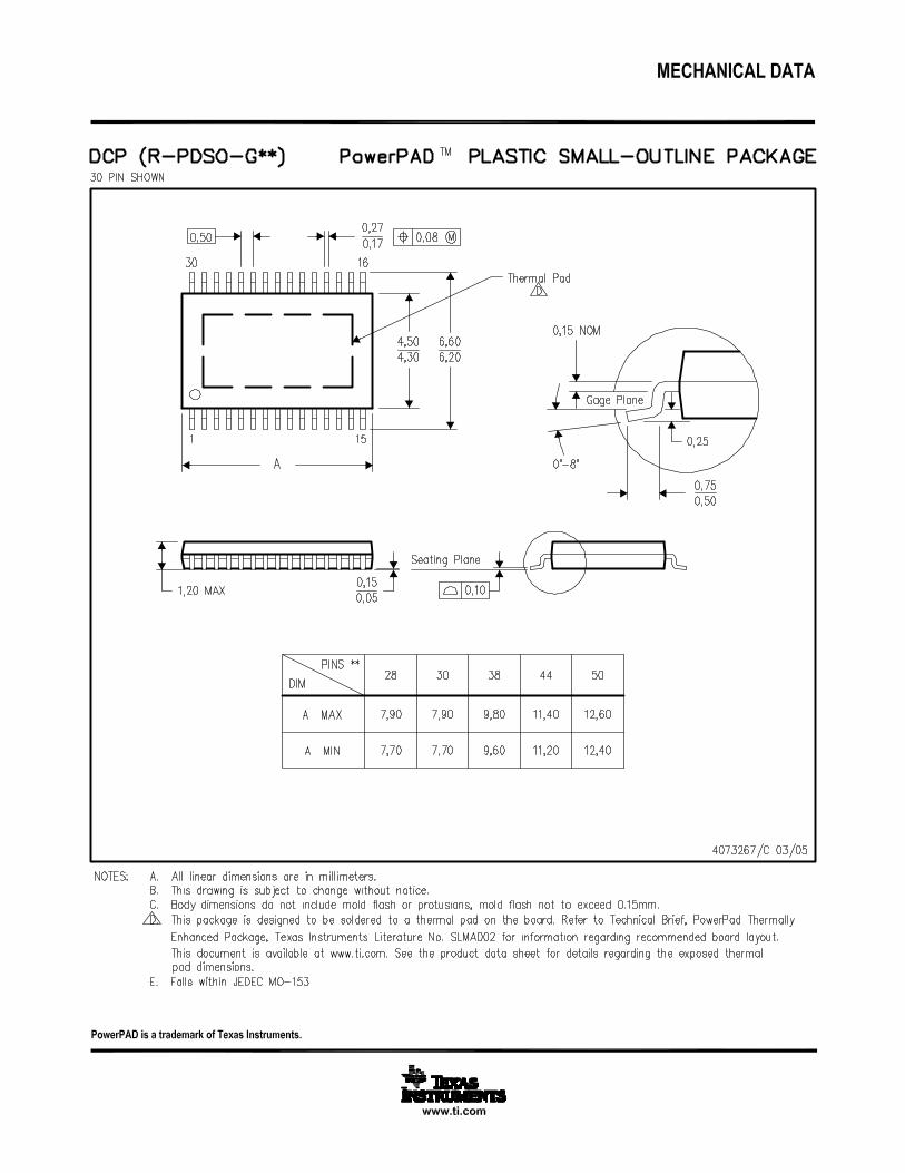
DCP (HTSSOP) PACKAGE
4 Submit Documentation Feedback Copyright © 2013, Texas Instruments Incorporated
Product Folder Links: DRV8711

DRV8711
www.ti.com SLVSC40 –JUNE 2013
ABSOLUTE MAXIMUM RATINGS (1) (2) (3)
over operating free-air temperature range (unless otherwise noted)
DRV8711 UNIT
Power supply voltage range -0.6 to 60 V
Charge pump voltage range (CP1, CP2, VCP) -0.6 to VM + 12 V
5V regulator voltage (V5) -0.6 to 5.5 V
Internal regulator voltage (VINT) -0.6 to 2.0 V
Digital pin voltage range (SLEEPn, RESET, STEP/AIN1, DIR/AIN2, BIN1, BIN2, SCS, SCLK, SDATI, -0.6 to 5.5 VSDATO, FAULTn, STALLn/BEMFVn)
High-side gate drive pin voltage range (A1HS, A2HS, B1HS, B2HS) -0.6 to VM + 12 V
Low-side gate drive pin voltage range (A1LS, A2LS, B1LS, B2LS) -0.6 to 12 V
Phase node pin voltage range (AOUT1, AOUT2, BOUT1, BOUT2) -0.6 to VM V
ISENSEx pin voltage (AISENP, AISENN, BISENP, BISENN) -0.7 to +0.7 V
BEMF pin voltage range (BEMF) -0.6 to VM V
Operating virtual junction temperature range, TJ -40 to 150 °C
Storage temperature range, Tstg -60 to 150 °C
(1) Stresses beyond those listed under "absolute maximum ratings" may cause permanent damage to the device. These are stress ratingsonly, and functional operation of the device at these or any other conditions beyond those indicated under "recommended operatingconditions" is not implied. Exposure to absolute–maximum–rated conditions for extended periods may affect device reliability.
(2) All voltage values are with respect to network ground terminal.(3) Power dissipation and thermal limits must be observed.
THERMAL INFORMATIONDRV8711
THERMAL METRIC (1) DCP UNITS
38 PINS
θJA Junction-to-ambient thermal resistance (2) 32.7
θJCtop Junction-to-case (top) thermal resistance (3) 17.2
θJB Junction-to-board thermal resistance (4) 14.3°C/W
ψJT Junction-to-top characterization parameter (5) 0.5
ψJB Junction-to-board characterization parameter (6) 14.1
θJCbot Junction-to-case (bottom) thermal resistance (7) 0.9
(1) For more information about traditional and new thermal metrics, see the IC Package Thermal Metrics application report, SPRA953.(2) The junction-to-ambient thermal resistance under natural convection is obtained in a simulation on a JEDEC-standard, high-K board, as
specified in JESD51-7, in an environment described in JESD51-2a.(3) The junction-to-case (top) thermal resistance is obtained by simulating a cold plate test on the package top. No specific JEDEC-
standard test exists, but a close description can be found in the ANSI SEMI standard G30-88.(4) The junction-to-board thermal resistance is obtained by simulating in an environment with a ring cold plate fixture to control the PCB
temperature, as described in JESD51-8.(5) The junction-to-top characterization parameter, ψJT, estimates the junction temperature of a device in a real system and is extracted
from the simulation data for obtaining θJA, using a procedure described in JESD51-2a (sections 6 and 7).(6) The junction-to-board characterization parameter, ψJB, estimates the junction temperature of a device in a real system and is extracted
from the simulation data for obtaining θJA , using a procedure described in JESD51-2a (sections 6 and 7).(7) The junction-to-case (bottom) thermal resistance is obtained by simulating a cold plate test on the exposed (power) pad. No specific
JEDEC standard test exists, but a close description can be found in the ANSI SEMI standard G30-88.Spacer
RECOMMENDED OPERATING CONDITIONSover operating free-air temperature range (unless otherwise noted)
MIN NOM MAX UNIT
VM Motor power supply voltage range 8 52 V
IVS V5 external load current 0 10 mA
TA Operating ambient temperature range -40 85 °C
Copyright © 2013, Texas Instruments Incorporated Submit Documentation Feedback 5
Product Folder Links: DRV8711

DRV8711
SLVSC40 –JUNE 2013 www.ti.com
ELECTRICAL CHARACTERISTICSover operating free-air temperature range (unless otherwise noted)
PARAMETER TEST CONDITIONS MIN TYP MAX UNIT
Power Supplies
IVM VM operating supply current VM = 24 V 17 20 mA
IVMQ VM sleep mode supply current VM = 24 V, SLEEPn = 0 65 98 μA
VM rising 7.1 8VUVLO VM undervoltage lockout voltage V
VM falling 6.3
Internal Linear Regulators
V5 V5 output voltage VM ≥ 12 V, IOUT = 1 mA - 10 mA 4.8 5 5.2 V
VINT VINT voltage No external load – reference only 1.7 1.8 1.9 V
Logic-Level Inputs
VIL Input low voltage 0.8 V
VIH Input high voltage 1.5 V
VHYS Input hysteresis voltage 300 mV
IIL Input low current VIN = 0 V -5 5 μA
IIH Input high current VIN = 5 V 30 50 70 μA
SDATAO, STALLn, FAULTn OUTPUTS (Open-Drain Outputs)
VOL Output low voltage IO = 5 mA 0.5 V
IOH Output high leakage current VO = 3.3 V 1 µA
MOSFET Drivers
VOUTH High-side gate drive output voltage VM = 24 V, IO = 100 μA VM+10 V
VOUTL Low-side gate drive output voltage VM = 24 V, IO = 100 μA 10 V
DTIME = 00 400
DTIME = 01 450Output dead time digital delay (deadtDEAD nstime is enforced in analog circuits) DTIME = 10 650
DTIME = 11 850
IDRIVEP = 00 50
IDRIVEP = 01 100Peak output current gate driveIOUTH mA(source) IDRIVEP = 10 150
IDRIVEP = 11 200
IDRIVEN = 00 100
IDRIVEN = 01 150IOUTl Peak output current gate drive (sink) mA
IDRIVEN = 10 200
IDRIVEN = 11 400
TDRIVEP = 00 250
TDRIVEP = 01 500tDRIVE Peak current drive time (source) ns
TDRIVEP = 10 1000
TDRIVEP = 11 2000
TDRIVEN = 00 250
TDRIVEN = 01 500tDRIVE Peak current drive time (sink) ns
TDRIVEN = 10 1000
TDRIVEN = 11 2000
Motor Driver
tOFF PWM off time adjustment range Set by TOFF register 0.5 128 μs
tBLANK Current sense blanking time Set by TBLANK register 0.5 5.12 μs
6 Submit Documentation Feedback Copyright © 2013, Texas Instruments Incorporated
Product Folder Links: DRV8711

DRV8711
www.ti.com SLVSC40 –JUNE 2013
ELECTRICAL CHARACTERISTICS (continued)over operating free-air temperature range (unless otherwise noted)
PARAMETER TEST CONDITIONS MIN TYP MAX UNIT
Protection Circuits
OCPTH = 00 160 250 320
OCPTH = 01 380 500 580Overcurrent protection trip levelVOCP mV(Voltage drop across external FET) OCPTH = 10 620 750 850
OCPTH = 11 840 1000 1200
tTSD Thermal shutdown temperature (1) Die temperature 150 160 180 °C
tHYS Thermal shutdown hysteresis 20 °C
Current Sense Amplifiers
ISGAIN = 00 5
ISGAIN = 01 10AV Gain V/V
ISGAIN = 10 20
ISGAIN = 11 40
ISGAIN = 00, ΔVIN = 400 mV 150
ISGAIN = 01, ΔVIN = 200 mV 300 nstSET Settling time (to ±1%)
ISGAIN = 10, ΔVIN = 100 mV 600
ISGAIN = 11, ΔVIN = 50 mV 1.2 µs
VOFS Offset voltage ISGAIN = 00, input shorted 4 mV
VIN Input differential voltage range -300 300 mV
Current Control DACs
Resolution 256 steps
Full-scale step response 10% to 90% 5 µs
VREF Full-scale (reference) voltage 2.50 2.75 3 V
(1) Not tested in production - guaranteed by design.
Copyright © 2013, Texas Instruments Incorporated Submit Documentation Feedback 7
Product Folder Links: DRV8711

XX
SCLK
SDATI
1
3
4
2
SCS
5
6 7 8
SDATOSDATO
valid
9
DRV8711
SLVSC40 –JUNE 2013 www.ti.com
SPI INTERFACE TIMING REQUIREMENTSover operating free-air temperature range (unless otherwise noted)
No. PARAMETER CONDITIONS MIN MAX UNIT
1 tCYC Clock cycle time 250 ns
2 tCLKH Clock high time 25 ns
3 tCLKL Clock low time 25 ns
4 tSU(SDATI) Setup time, SDATI to SCLK 5 ns
5 tH(SDATI) Hold time, SDATI to SCLK 1 ns
6 tSU(SCS) Setup time, SCS to SCLK 5 ns
7 tH(SCS) Hold time, SCS to SCLK 1 ns
8 tL(SCS) Inactive time, SCS (between writes) 100 ns
9 tD(SDATO) Delay time, SCLK to SDATO (during read) 10 ns
tSLEEP Wake time (SLEEPn inactive to high-side gate drive enabled) 1 ms
tRESET Delay from power-up or RESETn high until serial interface functional 10 μs
8 Submit Documentation Feedback Copyright © 2013, Texas Instruments Incorporated
Product Folder Links: DRV8711

STEP
DIR, MODE
2 3
1
4 5
DRV8711
www.ti.com SLVSC40 –JUNE 2013
INDEXER TIMING REQUIREMENTSover operating free-air temperature range (unless otherwise noted)
No. PARAMETER CONDITIONS MIN MAX UNIT
1 fSTEP Step frequency 250 kHz
2 tWH(STEP) Pulse duration, STEP high 1.9 μs
3 tWL(STEP) Pulse duration, STEP low 1.9 μs
4 tSU(STEP) Setup time, command to STEP rising 200 ns
5 tH(STEP) Hold time, command to STEP rising 200 ns
Copyright © 2013, Texas Instruments Incorporated Submit Documentation Feedback 9
Product Folder Links: DRV8711
xOUT1Gate
Drive
&
OCP
PWM
logic
x1HSVM
x1LS
xOUT2
x2HSVM
x2LS
Gate
Drive
&
OCP
ISEN
amp
+
-
xISENP
Comp
+
-
+
-
Comp
+
-
xISENN
X
Torque
DAC
VREF ISGAIN
TORQUE
RISENSE
1 V
xIN1
xIN2
DRV8711
SLVSC40 –JUNE 2013 www.ti.com
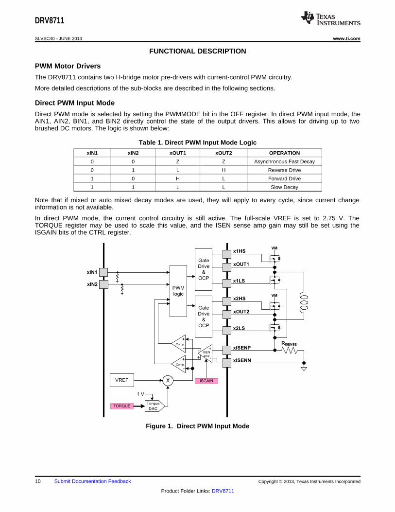
FUNCTIONAL DESCRIPTION
PWM Motor Drivers
The DRV8711 contains two H-bridge motor pre-drivers with current-control PWM circuitry.
More detailed descriptions of the sub-blocks are described in the following sections.
Direct PWM Input Mode
Direct PWM mode is selected by setting the PWMMODE bit in the OFF register. In direct PWM input mode, theAIN1, AIN2, BIN1, and BIN2 directly control the state of the output drivers. This allows for driving up to twobrushed DC motors. The logic is shown below:
Table 1. Direct PWM Input Mode Logic
xIN1 xIN2 xOUT1 xOUT2 OPERATION
0 0 Z Z Asynchronous Fast Decay
0 1 L H Reverse Drive
1 0 H L Forward Drive
1 1 L L Slow Decay
Note that if mixed or auto mixed decay modes are used, they will apply to every cycle, since current changeinformation is not available.
In direct PWM mode, the current control circuitry is still active. The full-scale VREF is set to 2.75 V. TheTORQUE register may be used to scale this value, and the ISEN sense amp gain may still be set using theISGAIN bits of the CTRL register.
Figure 1. Direct PWM Input Mode
10 Submit Documentation Feedback Copyright © 2013, Texas Instruments Incorporated
Product Folder Links: DRV8711

CHOP
ISENSE
2.75V TORQUEI
256 ISGAIN R
·
=
· ·
DRV8711
www.ti.com SLVSC40 –JUNE 2013
The current through the motor windings is regulated by an adjustable fixed-off-time PWM current regulationcircuit. When an H-bridge is enabled, current rises through the winding at a rate dependent on the DC voltageand inductance of the winding and the magnitude of the back EMF present. Once the current hits the currentchopping threshold, the bridge disables the current for a fixed period of time, which is programmable between500 nS and 128 µS by writing to the TOFF bits in the OFF register. After the off time expires, the bridge is re-enabled, starting another PWM cycle.
The chopping current is set by a comparator which compares the voltage across a current sense resistorconnected to the xISENx pins, multiplied by the gain of the current sense amplifier, with a reference voltage. Thecurrent sense amplifier is programmable in the CTRL register.
When driving in PWM mode, the chopping current is calculated as follows:
(1)
Where TORQUE is the setting of the TORQUE bits, and ISGAIN is the programmed gain of the ISENSEamplifiers (5, 10, 20, or 40).
Microstepping Indexer
Built-in indexer logic in the DRV8711 allows a number of different stepping configurations. The MODE bits in theCTRL register are used to configure the stepping format as shown in the table below:
Table 2. Microstepping Indexer Logic
MODE3 MODE2 MODE1 MODE0 STEP MODE
Full step (2-phase excitation)0 0 0 0 with 71% current
0 0 0 1 1/2 step
0 0 1 0 1/4 step
0 0 1 1 1/8 step
0 1 0 0 1/16 step
0 1 0 1 1/32 step
0 1 1 0 1/64 step
0 1 1 1 1/128 step
1 0 0 0 1/256 step
Copyright © 2013, Texas Instruments Incorporated Submit Documentation Feedback 11
Product Folder Links: DRV8711
DRV8711
SLVSC40 –JUNE 2013 www.ti.com
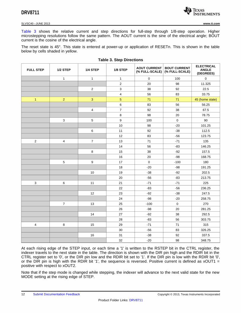
Table 3 shows the relative current and step directions for full-step through 1/8-step operation. Highermicrostepping resolutions follow the same pattern. The AOUT current is the sine of the electrical angle; BOUTcurrent is the cosine of the electrical angle.
The reset state is 45°. This state is entered at power-up or application of RESETn. This is shown in the tablebelow by cells shaded in yellow.
Table 3. Step Directions
ELECTRICALAOUT CURRENT BOUT CURRENTFULL STEP 1/2 STEP 1/4 STEP 1/8 STEP ANGLE(% FULL-SCALE) (% FULL-SCALE) (DEGREES)
1 1 1 0 100 0
2 20 98 11.325
2 3 38 92 22.5
4 56 83 33.75
1 2 3 5 71 71 45 (home state)
6 83 56 56.25
4 7 92 38 67.5
8 98 20 78.75
3 5 9 100 0 90
10 98 -20 101.25
6 11 92 -38 112.5
12 83 -56 123.75
2 4 7 13 71 -71 135
14 56 -83 146.25
8 15 38 -92 157.5
16 20 -98 168.75
5 9 17 0 -100 180
18 -20 -98 191.25
10 19 -38 -92 202.5
20 -56 -83 213.75
3 6 11 21 -71 -71 225
22 -83 -56 236.25
12 23 -92 -38 247.5
24 -98 -20 258.75
7 13 25 -100 0 270
26 -98 20 281.25
14 27 -92 38 292.5
28 -83 56 303.75
4 8 15 29 -71 71 315
30 -56 83 326.25
16 31 -38 92 337.5
32 -20 98 348.75
At each rising edge of the STEP input, or each time a '1' is written to the RSTEP bit in the CTRL register, theindexer travels to the next state in the table. The direction is shown with the DIR pin high and the RDIR bit in theCTRL register set to '0', or the DIR pin low and the RDIR bit set to '1'. If the DIR pin is low with the RDIR bit '0',or the DIR pin is high with the RDIR bit '1', the sequence is reversed. Positive current is defined as xOUT1 =positive with respect to xOUT2.
Note that if the step mode is changed while stepping, the indexer will advance to the next valid state for the newMODE setting at the rising edge of STEP.
12 Submit Documentation Feedback Copyright © 2013, Texas Instruments Incorporated
Product Folder Links: DRV8711
FS
ISENSE
2.75V TORQUEI
256 ISGAIN R
·
=
· ·
xOUT1
Gate Drive
&OCP
PWM logic
x1HSVM
x1LS
xOUT2
x2HSVM
x2LS
Gate Drive
&OCP
ISENamp
+
-
xISENP
Comp
+
-
SIN
DAC
+-
Comp
+
-
xISENN
X
Torque
DAC
Indexer ISGAIN
TORQUE
Registers
RISENSE
2.75 V
1 V
DRV8711
www.ti.com SLVSC40 –JUNE 2013
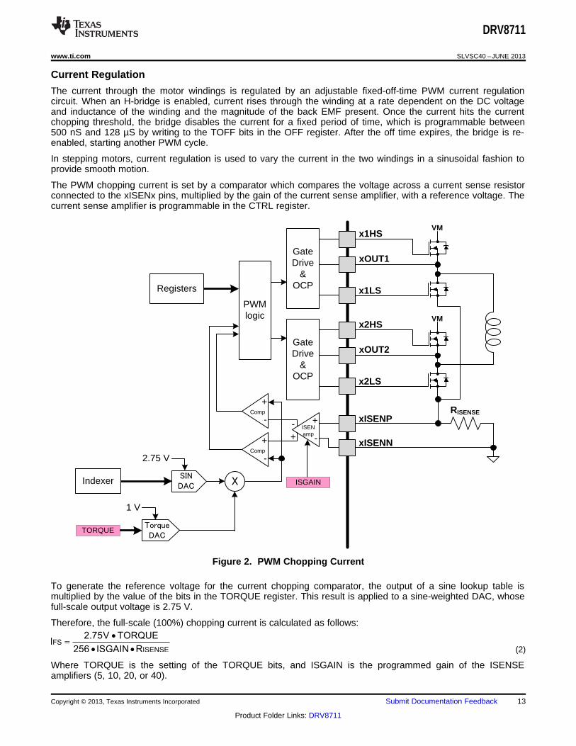
Current Regulation
The current through the motor windings is regulated by an adjustable fixed-off-time PWM current regulationcircuit. When an H-bridge is enabled, current rises through the winding at a rate dependent on the DC voltageand inductance of the winding and the magnitude of the back EMF present. Once the current hits the currentchopping threshold, the bridge disables the current for a fixed period of time, which is programmable between500 nS and 128 µS by writing to the TOFF bits in the OFF register. After the off time expires, the bridge is re-enabled, starting another PWM cycle.
In stepping motors, current regulation is used to vary the current in the two windings in a sinusoidal fashion toprovide smooth motion.
The PWM chopping current is set by a comparator which compares the voltage across a current sense resistorconnected to the xISENx pins, multiplied by the gain of the current sense amplifier, with a reference voltage. Thecurrent sense amplifier is programmable in the CTRL register.
Figure 2. PWM Chopping Current
To generate the reference voltage for the current chopping comparator, the output of a sine lookup table ismultiplied by the value of the bits in the TORQUE register. This result is applied to a sine-weighted DAC, whosefull-scale output voltage is 2.75 V.
Therefore, the full-scale (100%) chopping current is calculated as follows:
(2)
Where TORQUE is the setting of the TORQUE bits, and ISGAIN is the programmed gain of the ISENSEamplifiers (5, 10, 20, or 40).
Copyright © 2013, Texas Instruments Incorporated Submit Documentation Feedback 13
Product Folder Links: DRV8711

xOUT1 xOUT2
3
1
2
3
Drive Current
Slow decay (brake)
Fast decay (reverse)
VM
1
2
Slow Decay
Fast Decay
Mixed Decay
PWM
ON PWM OFF
TOFF
Itrip
TDECAY
TBLANK
DRV8711
SLVSC40 –JUNE 2013 www.ti.com
Example:
If a 0.1-Ω sense resistor is used, ISGAIN is set to 0 (gain of 5), and TORQUE is set to 255, the full-scale (100%)chopping current will be (2.75V * 255) / (256 * 5 * 0.1Ω) = 5.5A.
Decay Modes
During PWM current chopping, the H-bridge is enabled to drive through the motor winding until the PWM currentchopping threshold is reached. This is shown in Figure 3, Item 1. The current flow direction shown indicatespositive current flow in the step table below.
Once the chopping current threshold is reached, the H-bridge can operate in two different states, fast decay orslow decay.
In fast decay mode, once the PWM chopping current level has been reached, the H-bridge reverses state toallow winding current to flow in a reverse direction. If synchronous rectification is enabled (SRn pin logic low), theopposite FETs are turned on; as the winding current approaches zero, the bridge is disabled to prevent anyreverse current flow. If SRn is high, current is recirculated through the body diodes, or through external Schottkydiodes. Fast-decay mode is shown in Figure 3, Item 2.
In slow-decay mode, winding current is re-circulated by enabling both of the low-side FETs in the bridge. This isshown in Figure 3, Item 3.
Figure 3. Decay Modes
The DRV8711 supports fast decay and slow decay modes in both indexer and direct PWM modes. In addition, inindexer mode only, it supports fixed mixed decay and auto mixed decay modes. Decay mode is selected by theDECMOD bits in the DECAY register.
Mixed decay mode begins as fast decay, but after a programmable period of time (set by the TDECAY bits in theDECAY register) switches to slow decay mode for the remainder of the fixed off time. Even if mixed decay isselected, if the current is increasing or remaining the same (per the step table), then slow decay is used.
Auto mixed decay mode samples the current level at the end of the blanking time, and if the current is above theItrip threshold, immediately changes the H-bridge to fast decay. During fast decay, the (negative) current ismonitored, and when it falls below the Itrip threshold (and another blanking time has passed), the bridge isswitched to slow decay. Once the fixed off time expires, a new cycle is started.
If the bridge is turned on and at the end of TBLANK the current is below the Itrip threshold, the bridge remains onuntil the current reaches Itrip. Then slow decay is entered for the fixed off time, and a new cycle begins.
Refer to Figure 4 and Figure 5.
14 Submit Documentation Feedback Copyright © 2013, Texas Instruments Incorporated
Product Folder Links: DRV8711

tOFFtBLANK
tON
Itrip increase tBLANK
tON
Itrip
Itrip decrease tOFFtBLANK
tON
Decrease in Itrip terminates
cycle, fast decay begins
Itrip
When I < Itrip in fast decay
change to slow decay
tBLANK
tON
tOFF
Increase in Itrip terminates
cycle, bridge turns on
On
Fast
Decay
Slow
Decay
tOFFI below Itrip
after tBLANK
I above Itrip
after tBLANK
tBLANK tOFF
tOFFOn
Fast
Decay
Slow
Decay
tBLANK tBLANK
tON
Itrip
tBLANK
tON
Itrip
tOFF
I < ItripAt Itrip and after
tBLANK, slow decay
I > Itrip, start
fast decayWhen I < Itrip in fast decay
and tBLANK expires, change
to slow decay
tON
tBLANK tBLANK
tON
DRV8711
www.ti.com SLVSC40 –JUNE 2013
The upper waveform shows the behavior if I < Itrip at the end of tBLANK. Note that (at slow motor speeds, whereback EMF is not significant), the current increase during the ON phase is the same magnitude as the currentdecrease in fast decay, since both times are controlled by tBLANK, and the rate of change is the same (full VM isapplied to the load inductance in both cases, but in opposite directions). In this case, the current will gradually bedriven down until the peak current is just hitting Itrip at the end of the blanking time, after which some cycles willbe slow decay, and some will be mixed decay.
Figure 4. I < Itrip at the End of tBLANK
If the Itrip level changes during a PWM cycle (in response to a step command to the indexer), the current cycle isimmediately terminated, and a new cycle is begun. Refer to the drawing below.
If the Itrip level has increased, the H-bridge will immediately turn on; if the Itrip level has decreased, fast decaymode is begun immediately. The top waveform shows what happens when the Itrip threshold decreases during aPWM cycle. The lower Itrip level results in the current being above the Itrip threshold at the end of tBLANK onthe following cycle. Fast decay is entered until the current is driven below the Itrip threshold.
Figure 5. Itrip Level Changing During a PWM Cycle
Copyright © 2013, Texas Instruments Incorporated Submit Documentation Feedback 15
Product Folder Links: DRV8711

DRV8711
SLVSC40 –JUNE 2013 www.ti.com
Blanking Time
After the current is enabled in an H-bridge, the voltage on the ISEN pin is ignored for a period of time beforeenabling the current sense circuitry. This blanking time is adjustable from 1 µS to 5.12 µs, in 20 ns increments,by setting the TBLANK bits in the BLANK register. Note that the blanking time also sets the minimum on time ofthe PWM.
The same blanking time is applied to the fast decay period in auto decay mode. The PWM will ignore anytransitions on Itrip after entering fast decay mode, until the blanking time has expired.
To provide better current control at very low current steps, an adaptive blanking time mode can be enabled bysetting the ABT bit in the BLANK register. If ABT is set, at current levels below 30% of full scale current (asdetermined by the step table), the blanking time (so also the minimum on time) is cut in half, to 50% of the valueprogrammed by the TBLANK bits.
For higher degrees of micro-stepping it is recommended to enable ABT bit for better current regulation.
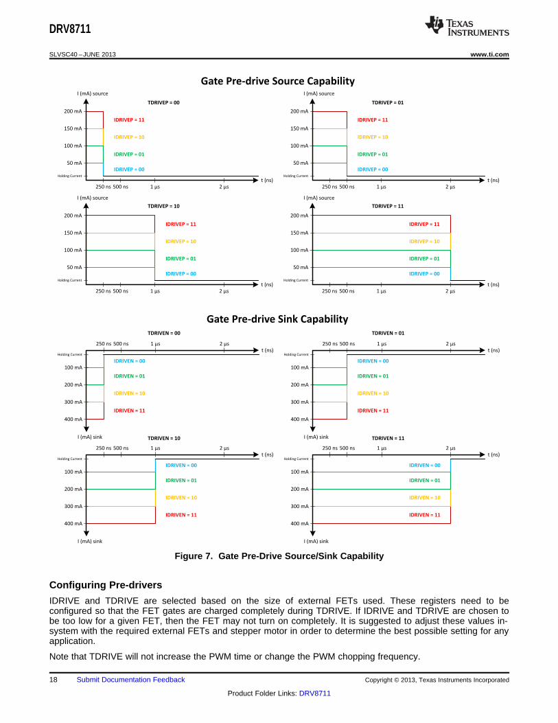
Pre-Drivers
An internal charge pump circuit and pre-drivers inside the DRV8711 directly drive N-channel MOSFETs, whichdrive the motor current.
The peak drive current of the pre-drivers is adjustable by setting the bits in the DRIVE register. Peak sourcecurrents may be set to 50 mA, 100 mA, 150 mA, or 200 mA. The peak sink current is approximately 2x the peaksource current. Adjusting the peak current will change the output slew rate, which also depends on the FET inputcapacitance and gate charge.
When changing the state of the output, the peak current is applied for a short period of time (tDRIVE), to chargethe gate capacitance. After this time, a weak current source is used to keep the gate at the desired state. Whenselecting the gate drive strength for a given external FET, the selected current must be high enough to fullycharge and discharge the gate during the time when driven at full current, or excessive power will be dissipatedin the FET.
During high-side turn-on, the low-side gate is pulled low. This prevents the gate-source capacitance of the low-side FET from inducing turn-on.
The pre-driver circuits include enforcement of a dead time in analog circuitry, which prevents the high-side andlow-side FETs from conducting at the same time. Additional dead time is added with digital delays. This delaycan be selected by setting the DTIME bits in the CTRL register.
16 Submit Documentation Feedback Copyright © 2013, Texas Instruments Incorporated
Product Folder Links: DRV8711

Low
Z
Low ZHigh Z High Z High Z
High Z High ZLow Z High Z
Low
Z
tDEAD tDEAD
xHS
(V)
xLS
(V)
HS drive
(mA)
LS drive
(mA)
tDRIVE
tDRIVE
DRV8711
www.ti.com SLVSC40 –JUNE 2013
Figure 6. Pre-Drivers
Copyright © 2013, Texas Instruments Incorporated Submit Documentation Feedback 17
Product Folder Links: DRV8711
t (ns)
I (mA) source
200 mA
150 mA
100 mA
50 mA
Holding Current
250 ns 500 ns 1 µs 2 µs
t (ns)
I (mA) source
200 mA
150 mA
100 mA
50 mA
Holding Current
250 ns 500 ns 1 µs 2 µs
t (ns)
I (mA) source
200 mA
150 mA
100 mA
50 mA
250 ns 500 ns 1 µs 2 µs
t (ns)
I (mA) source
200 mA
150 mA
100 mA
50 mA
Holding Current
250 ns 500 ns 1 µs 2 µs
TDRIVEP = 00 TDRIVEP = 01
TDRIVEP = 10 TDRIVEP = 11
IDRIVEP = 11
IDRIVEP = 10
IDRIVEP = 01
IDRIVEP = 00
IDRIVEP = 11
IDRIVEP = 10
IDRIVEP = 01
IDRIVEP = 00
IDRIVEP = 11
IDRIVEP = 10
IDRIVEP = 01
IDRIVEP = 00
IDRIVEP = 11
IDRIVEP = 10
IDRIVEP = 01
IDRIVEP = 00
250 ns
t (ns)
I (mA) sink
400 mA
300 mA
200 mA
100 mA
Holding Current
250 ns 500 ns 1 µs 2 µs
t (ns)
I (mA) sink
400 mA
300 mA
200 mA
100 mA
Holding Current
250 ns 500 ns 1 µs 2 µs
t (ns)
I (mA) sink
400 mA
300 mA
200 mA
100 mA
500 ns 1 µs 2 µs
t (ns)
I (mA) sink
400 mA
300 mA
200 mA
100 mA
Holding Current
250 ns 500 ns 1 µs 2 µs
TDRIVEN = 00 TDRIVEN = 01
TDRIVEN = 10 TDRIVEN = 11
IDRIVEN = 11
IDRIVEN = 10
IDRIVEN = 01
IDRIVEN = 00
IDRIVEN = 11
IDRIVEN = 10
IDRIVEN = 01
IDRIVEN = 00
IDRIVEN = 11
IDRIVEN = 10
IDRIVEN = 01
IDRIVEN = 00
IDRIVEN = 11
IDRIVEN = 10
IDRIVEN = 01
IDRIVEN = 00
Holding Current
Holding Current
Gate Pre-drive Sink Capability
Gate Pre-drive Source Capability
DRV8711
SLVSC40 –JUNE 2013 www.ti.com
Figure 7. Gate Pre-Drive Source/Sink Capability
Configuring Pre-drivers
IDRIVE and TDRIVE are selected based on the size of external FETs used. These registers need to beconfigured so that the FET gates are charged completely during TDRIVE. If IDRIVE and TDRIVE are chosen tobe too low for a given FET, then the FET may not turn on completely. It is suggested to adjust these values in-system with the required external FETs and stepper motor in order to determine the best possible setting for anyapplication.
Note that TDRIVE will not increase the PWM time or change the PWM chopping frequency.
18 Submit Documentation Feedback Copyright © 2013, Texas Instruments Incorporated
Product Folder Links: DRV8711

20mA (2 DTIME TBLANK TOFF)Q
4
· · + +<
DRV8711
www.ti.com SLVSC40 –JUNE 2013
In a system with capacitor charge Q and desired rise time RT, IDRIVE and TDRIVE can be initially selectedbased on:
IDRIVE > Q / RT
TDRIVE > 2 x RT
For best results, select the smallest IDRIVE and TDRIVE that meet the above conditions.
Example:
If the gate charge is 15 nC and the desired rise time is 400 ns, then select:
IDRIVEP = 50 mA, IDRIVEN = 100 mA
TDRIVEP = TDRIVEN = 1 µs
External FET Selection
In a typical setup, the DRV8711 can support external FETs over 50 nC each. However, this capacity can belower or higher based on the device operation. For an accurate calculation of FET driving capacity, use thefollowing equation.
(3)
Example:
If a DTIME is set to 0 (400 ns), TBLANK is set to 0 (1 µs), and TOFF is set to 0 (500 ns), then the DRV8711 willsupport Q < 11.5 nC FETs (please note that this is an absolute worst-case scenario with a PWM frequency~ 430 kHz).
If a DTIME is set to 0 (400 ns), TBLANK is set to 0 (1 µs), and TOFF is set to 0x14 (10 µs), then the DRV8711will support Q < 59 nC FETs (PWM frequency ~ 85 kHz).
If a DTIME is set to 0 (400 ns), TBLANK is set to 0 (1 µs), and TOFF is set to 0x60 (48 µs), then the DRV8711will support Q < 249 nC FETs (PWM frequency ~ 20 kHz).
Stall Detection
The DRV8711 implements a back EMF monitoring scheme that is capable of detecting a stall during steppermotor motion. This stall detection is intended to be used to get an indication when a motor is run into amechanical stop, or when an increased torque load on the motor causes it to stall.
To determine that a stall has occurred, a drop in motor back EMF is detected. The DRV8711 supports twomethods of this detection: an automatic internal stall detection circuit, or the ability to use an externalmicrocontroller to monitor back EMF.
During a zero-current step, one side of the H-bridge is placed in a high impedance state, and the opposite low-side FET is turned on for a brief duration defined by TORQUE register SMPLTH bit [10:8]. This allows the currentto decay quickly through the low-side FET and the opposite body diode. Which side of the bridge is tri-state andwhich one is driven low depends on the current direction on the previous step. The bridge with the high side thathas been actively PWMed (at the beginning of the PWM cycle during blank time) prior to entering the zero-current step will be held low and the opposite side will be tri-stated.
Back EMF is sampled on the tri-stated output pin at the end of SMPLTH time (TORQUE register bit [10:8]). Theback EMF from the selected pin is divided by 4, 8, 16, or 32, depending on the setting of the VDIV bits in theSTALL register. The voltage is buffered and held on an external capacitor placed on the BEMF pin. The signal onthe BEMF output pin can be further processed by a microcontroller to implement more advanced control and stalldetection algorithms.
Copyright © 2013, Texas Instruments Incorporated Submit Documentation Feedback 19
Product Folder Links: DRV8711

AOUT1
Step
Motor
VM
AOUT2
VM
DAC
8
reference
1.80 V
SDTHR
DAC
SDTHR
BOUT1
VM
BOUT2
VM
bufferBEMF
control
logic
comp
+
-counter
STALLn/
BEMFVn
SDCNT
2
VDIV
2
VDIV
2
VDIV
2
VDIV
2
To
STATUS
register
DRV8711
SLVSC40 –JUNE 2013 www.ti.com
Figure 8. Stall Detection
Internal Stall Detection
To use internal stall detection, the EXSTALL bit in the CTRL register is set to ‘0’. In this mode, theSTALLn/BEMFVn output pin is used to signal a valid stall condition.
Step time, or rate at which step input is applied to DRV8711, has to be greater than SMPLTH time for back EMFsampling.
Using internal stall detection, a stall is detected when the sampled back EMF drops below the value set by theSDTHR bits in the STALL register. A programmable counter circuit allows the assertion of the STALLn output tobe delayed until the back EMF has been sampled below the SDTHR value for more than one zero-current step.The counter is programmed by the SDCNT bits in the STALL register, and provides selections of 1, 2, 4, or 8steps.
When the stall is detected (at the end of a SMPLTH interval), the STALLn/BEMFVn pin is driven active low, andthe STD bit and the STDLAT bit in the STATUS register are set. The STALLn/BEMFVn pin will deassert and theSTD bit will automatically clear at the next zero-current step if a stall condition is not detected, while the STDLATbit will remain set until a '0' is written to it. The STDLAT is reset when the STD bit clears after the first zero-crossstep that does not detect a stall condition.
This stall detection scheme is only effective when the motor is stalled while running at or above some minimumspeed. Since it relies on detecting a drop in motor back EMF, the motor must be rotating with sufficient speed togenerate a detectable back EMF. During motor start-up, and at very slow step rates, the stall detection is notreliable.
Since back EMF can only be sampled during a zero-current state, stall detection is not possible in full step mode.During full-step operation, the stall detect circuit is gated off to prevent false signaling of a stall.
The correct setting of the SDTHR bits needs to be determined experimentally. It is dependent on many factors,including the electrical and mechanical characteristics of the load, the peak current setting, and the supplyvoltage.
20 Submit Documentation Feedback Copyright © 2013, Texas Instruments Incorporated
Product Folder Links: DRV8711

DRV8711
www.ti.com SLVSC40 –JUNE 2013
External Stall Detection
To use an external microcontroller to manage stall detection, the EXSTALL bit in the CTRL register is set to ‘1’.In this mode, the STALLn / BEMFVn output pin is used to signal a valid back EMF measurement is ready. Inaddition, the SDT and SDTLAT bits are also set at this time.
BEMFVn and BEMF are still valid outputs in this mode even if the step time is smaller than SMPLTH time.
When the BEMFVn pin goes active low, it is an indication that a valid back EMF voltage measurement isavailable. This signal could be used, for example, to trigger an interrupt on a microcontroller. The microcontrollercan then sample the voltage present (using an A/D converter) on the BEMF pin.
After sampling the back EMF voltage, the microcontroller writes a ‘0’ to the SDTLAT bit to clear the SDT bit andBEMFVn pin, in preparation for the next back EMF sample. If the SDTLAT bit is not cleared by themicrocontroller, it will automatically be cleared in the next zero-current step.
For either internal or external stall detection, at very high motor speeds when the PWM duty cycle approaches100%, the inductance of the motor and the short duration of each step may cause the time required for currentrecirculation to exceed the step time. In this case, back EMF will not be correctly sampled, and stall detectioncannot function. This condition occurs most at high degrees of micro-stepping, since the zero current step lastsfor a shorter duration. It is advisable to run the motor at lower degrees of micro-stepping at higher speeds toallow time for current recirculation if stall detection is needed in this condition.
RESET and SLEEPn Operation
An internal power-up reset circuit monitors the voltage applied to the VM pin. If VM falls below the VMundervoltage lockout voltage, the part is reset, as described below for the case of asserting the RESET pin.
If the RESET pin is asserted, all internal logic including the indexer is reset. All registers are returned to theirinitial default conditions. The power stage will be disabled, and all inputs, including STEP and the serial interface,are ignored when RESET is active.
On exiting reset state, some time (approximately 1 mS) needs to pass before the part is fully functional.
Applying an active low input to the SLEEPn input pin will place the device into a low power state. In sleep mode,the motor driver circuitry is disabled, the gate drive regulator and charge pump are disabled, and all analogcircuitry is placed into a low power state. The digital circuitry in the device still operates, so the device registerscan still be accessed via the serial interface.
When SLEEPn is active, the RESET pin does not function. SLEEPn must be exited before RESET will takeeffect.
When exiting from sleep mode, some time (approximately 1 mS) needs to pass before applying a STEP input, toallow the internal circuitry to stabilize.
Copyright © 2013, Texas Instruments Incorporated Submit Documentation Feedback 21
Product Folder Links: DRV8711

1/4 stepping 1/8 stepping
1/16 stepping 1/128 stepping
STEP STEP
STEP STEP
Current Current
Current Current
DRV8711
SLVSC40 –JUNE 2013 www.ti.com
Microstepping Drive Current
The following plots are examples of stepper motor current in one of the windings. Since these waveforms aredependent on DRV8711 register settings as well as the external FETs, sense resistor, and stepper motor, theyshould only be used as a reference.
Figure 9. Microstepping Drive Current
22 Submit Documentation Feedback Copyright © 2013, Texas Instruments Incorporated
Product Folder Links: DRV8711

DRV8711
www.ti.com SLVSC40 –JUNE 2013
Protection Circuits
The DRV8711 is fully protected against undervoltage, overcurrent and overtemperature events.
Overcurrent Protection (OCP)
Overcurrent is sensed by monitoring the voltage drop across the external FETs. If the voltage across a drivenFET exceeds the value programmed by the OCPTH bits in the DRIVE register for more than the time periodspecified by the OCPDEG bits in the DRIVE register, an OCP event is recognized. When operating in directPWM mode, during an OCP event, the H-bridge experiencing the OCP event is disabled; if operating in indexermode, both H-bridges will be disabled. In addition, the corresponding xOCP bit in the STATUS register is set,and the FAULTn pin is driven low. The H-bridge(s) will remain off, and the xOCP bit will remain set, until it iswritten to 0, or the device is reset.
Pre-Driver Fault
If excessive current is detected on the gate drive outputs (which would be indicative of a failed/shorted outputFET or PCB fault), the H-bridge experiencing the fault is disabled, the xPDF bit in the STATUS register is set,and the FAULTn pin is driven low. The H-bridge will remain off, and the xPDF bit will remain set until it is writtento 0, or the device is reset.
Thermal Shutdown (TSD)
If the die temperature exceeds safe limits, all FETs in the H-bridge will be disabled, the OTS bit in the STATUSregister will be set, and the FAULTn pin will be driven low. Once the die temperature has fallen to a safe leveloperation will automatically resume and the OTS bit will reset. The FAULTn pin will be released after operationhas resumed.
Undervoltage Lockout (UVLO)
If at any time the voltage on the VM pin falls below the undervoltage lockout threshold voltage, all FETs in the H-bridge will be disabled, the UVLO bit in the STATUS register will be set, and the FAULTn pin will be driven low.Operation will resume and the UVLO bit will reset when VM rises above the UVLO threshold. The FAULTn pinwill be released after operat ion has resumed.
During any of these fault conditions, the STEP input pin will be ignored.
Copyright © 2013, Texas Instruments Incorporated Submit Documentation Feedback 23
Product Folder Links: DRV8711

SCS
SCLK
SDATI
1 2 3 4 5 6 9 11 12 13 614 15 16Note 1
READ A2 A1 A0
SDATO D5 D4 D3
10
D11 D10 D9 D8 D7 D6
7 8
D2 D1 D0
SCS
SCLK
SDATI
1 2 3 4 5 6 7 8 9 10 11 12 13 14 15 16
D3 D2 D1 D0
Note 1
WRT A2 A1 A0 D7 D6 D5 D4D11 D D9 D8 X10
DRV8711
SLVSC40 –JUNE 2013 www.ti.com
Serial Data Format
The serial data consists of a 16-bit serial write, with a read/write bit, 3 address bits and 12 data bits. The threeaddress bits identify one of the registers defined in the register section above.
To write to a register, data is shifted in after the address as shown in the timing diagram below:
A. Any amount of time may pass between bits, as long as SCS stays active high. This allows two 8-bit writes to be used.
Figure 10. Write Operation
Data may be read from the registers through the SDATO pin. During a read operation, only the address is usedform the SDATI pin; the data bits following are ignored. Reading is enabled by setting the READ bit at thebeginning of the access:
(1) Any amount of time may pass between bits, as long as SCS stays active high. This allows two 8-bit writes to be used.
Figure 11. Read Operation
24 Submit Documentation Feedback Copyright © 2013, Texas Instruments Incorporated
Product Folder Links: DRV8711
4 0123567891011Address
HexName
TORQUE
CTRL
Name
BLANK
OFF
STALL
DECAY
STATUS
DRIVE
01
00
Address
Hex
03
02
05
04
07
06
4 0123567891011
RW
RW
MODE
DRV8711 REGISTER MAP
SDTHR
RW
RW
RW
RW
RW
RW
RW
ENBL
OTSAOCPBOCP
RDIRRSTEP
UVLO
TORQUE
TOFF
TBLANK
OCPDEG OCPTH
ISGAIN
TDECAYDECMOD
Reserved
Reserved
Reserved
Reserved
DTIME
SDCNT
ABT
Reserved
VDIV
PWMMODE
STDSTDLAT APDFBPDF
TDRIVENTDRIVEPIDRIVENIDRIVEP
EXSTALL
SMPLTH
DRV8711
www.ti.com SLVSC40 –JUNE 2013
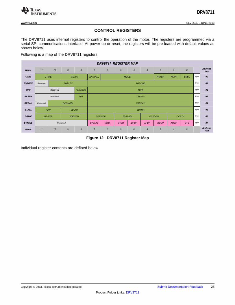
CONTROL REGISTERS
The DRV8711 uses internal registers to control the operation of the motor. The registers are programmed via aserial SPI communications interface. At power-up or reset, the registers will be pre-loaded with default values asshown below.
Following is a map of the DRV8711 registers:
Figure 12. DRV8711 Register Map
Individual register contents are defined below.
Copyright © 2013, Texas Instruments Incorporated Submit Documentation Feedback 25
Product Folder Links: DRV8711

DRV8711
SLVSC40 –JUNE 2013 www.ti.com
CTRL Register
Address = 0x00h
BIT NAME SIZE R/W DEFAULT DESCRIPTION
0: Disable motor0 ENBL 1 R/W 0 1: Enable motor
0: Direction set by DIR pin1 RDIR 1 R/W 0 1: Direction set by inverse of DIR pin
0: No action2 RSTEP 1 W 0 1: Indexer will advance one step; automatically cleared after write
0000: Full-step, 71% current0001: Half step0010: 1/4 step0011: 1/8 step0100: 1/16 step6-3 MODE 4 R/W 110 0101: 1/32 step0110: 1/64 step0111: 1/128 step1000: 1/256 step1001 – 1111: Reserved
0: Internal stall detect7 EXSTALL 1 R/W 0 1: External stall detect
ISENSE amplifier gain set00: Gain of 5
9-8 ISGAIN 2 R/W 0 01: Gain of 1010: Gain of 2011: Gain of 40
Dead time set00: 400 ns dead time
11-10 DTIME 2 R/W 11 01: 450 ns dead time10: 650 ns dead time11: 850 ns dead time
TORQUE Register
Address = 0x01h
BIT NAME SIZE R/W DEFAULT DESCRIPTION
7-0 TORQUE 8 R/W 0xFFh Sets full-scale output current for both H-bridges
Back EMF sample threshold000: 50 µs001: 100 µs010: 200 µs
10-8 SIMPLTH 3 R/W 1 011: 300 µs100: 400 µs101: 600 µs110: 800 µs111: 1000 µs
11 Reserved 1 - - Reserved
OFF Register
Address = 0x02h
BIT NAME SIZE R/W DEFAULT DESCRIPTION
Sets fixed off time, in increments of 500 ns7-0 TOFF 8 R/W 0x30h 0x00h: 500 ns
0xFFh: 128 µs
0: Use internal indexer8 PWMMODE 1 R/W 0 1: Bypass indexer, use xINx inputs to control outputs
11-9 Reserved 3 - - Reserved
26 Submit Documentation Feedback Copyright © 2013, Texas Instruments Incorporated
Product Folder Links: DRV8711
DRV8711
www.ti.com SLVSC40 –JUNE 2013
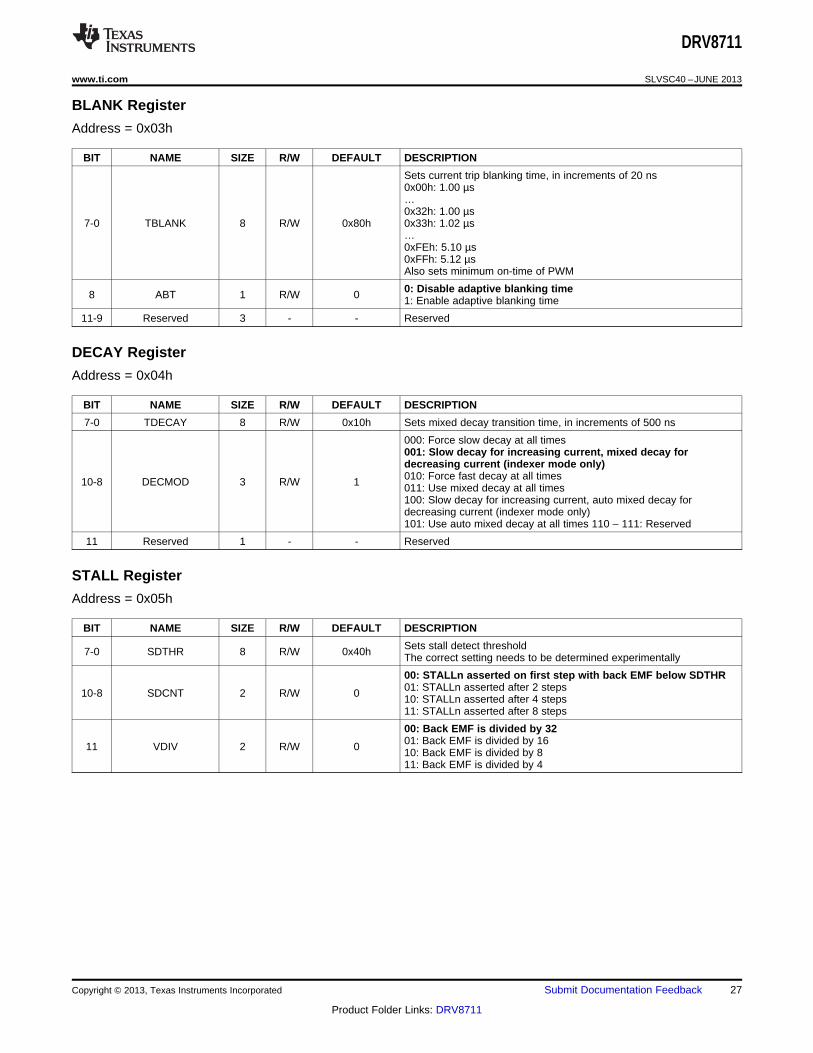
BLANK Register
Address = 0x03h
BIT NAME SIZE R/W DEFAULT DESCRIPTION
Sets current trip blanking time, in increments of 20 ns0x00h: 1.00 µs…0x32h: 1.00 µs
7-0 TBLANK 8 R/W 0x80h 0x33h: 1.02 µs…0xFEh: 5.10 µs0xFFh: 5.12 µsAlso sets minimum on-time of PWM
0: Disable adaptive blanking time8 ABT 1 R/W 0 1: Enable adaptive blanking time
11-9 Reserved 3 - - Reserved
DECAY Register
Address = 0x04h
BIT NAME SIZE R/W DEFAULT DESCRIPTION
7-0 TDECAY 8 R/W 0x10h Sets mixed decay transition time, in increments of 500 ns
000: Force slow decay at all times001: Slow decay for increasing current, mixed decay fordecreasing current (indexer mode only)010: Force fast decay at all times10-8 DECMOD 3 R/W 1 011: Use mixed decay at all times100: Slow decay for increasing current, auto mixed decay fordecreasing current (indexer mode only)101: Use auto mixed decay at all times 110 – 111: Reserved
11 Reserved 1 - - Reserved
STALL Register
Address = 0x05h
BIT NAME SIZE R/W DEFAULT DESCRIPTION
Sets stall detect threshold7-0 SDTHR 8 R/W 0x40h The correct setting needs to be determined experimentally
00: STALLn asserted on first step with back EMF below SDTHR01: STALLn asserted after 2 steps10-8 SDCNT 2 R/W 0 10: STALLn asserted after 4 steps11: STALLn asserted after 8 steps
00: Back EMF is divided by 3201: Back EMF is divided by 1611 VDIV 2 R/W 0 10: Back EMF is divided by 811: Back EMF is divided by 4
Copyright © 2013, Texas Instruments Incorporated Submit Documentation Feedback 27
Product Folder Links: DRV8711

DRV8711
SLVSC40 –JUNE 2013 www.ti.com
DRIVE Register
Address = 0x06h
BIT NAME SIZE R/W DEFAULT DESCRIPTION
OCP threshold00: 250 mV
1-0 OCPTH 2 R/W 0 01: 500 mV10: 750 mV11: 1000 mV
OCP deglitch time00: 1 µs
3-2 OCPDEG 2 R/W 10 01: 2 µs10: 4 µs11: 8 µs
Low-side gate drive time00: 250 ns
5-4 TDRIVEN 2 R/W 1 01: 500 ns10: 1 µs11: 2 µs
High-side gate drive time00: 250 ns
7-6 TDRIVEP 2 R/W 1 01: 500 ns10: 1 µs11: 2 µs
Low-side gate drive peak current00: 100 mA peak (sink)
9-8 IDRIVEN 2 R/W 0 01: 200 mA peak (sink)10: 300 mA peak (sink)11: 40 0mA peak (sink)
High-side gate drive peak current00: 50 mA peak (source)
11-10 IDRIVEP 2 R/W 0 01: 100 mA peak (source)10: 150 mA peak (source)11: 200 mA peak (source)
28 Submit Documentation Feedback Copyright © 2013, Texas Instruments Incorporated
Product Folder Links: DRV8711

DRV8711
www.ti.com SLVSC40 –JUNE 2013
STATUS Register
Address = 0x07h
BIT NAME SIZE R/W DEFAULT DESCRIPTION
0: Normal operation0 OTS 1 R 0 1: Device has entered overtemperature shutdown
OTS bit will clear once temperature has fallen to safe levels
0: Normal operation1 AOCP 1 R/W 0 1: Channel A overcurrent shutdown
Write a ‘0’ to this bit to clear the fault and resume operation
0: Normal operation2 BOCP 1 R/W 0 1: Channel B overcurrent shutdown
Write a ‘0’ to this bit to clear the fault and resume operation
0: Normal operation3 UVLO 1 R 0 1: Undervoltage lockout
UVLO bit will clear after VM has increased over VUVLO
0: Normal operation4 APDF 1 R/W 0 1: Channel A predriver fault
Write a ‘0’ to this bit to clear the fault and resume operation
0: Normal operation5 BPDF 1 R/W 0 1: Channel B predriver fault
Write a ‘0’ to this bit to clear the fault and resume operation
0: Normal operation6 STD 1 R 0 1: Stall detected
0: Normal operation7 STDLAT 1 R/W 0 1: Latched stall detect
Write a ‘0’ to this bit to clear the fault and resume operation
11-8 Reserved 4 - - Reserved
Copyright © 2013, Texas Instruments Incorporated Submit Documentation Feedback 29
Product Folder Links: DRV8711
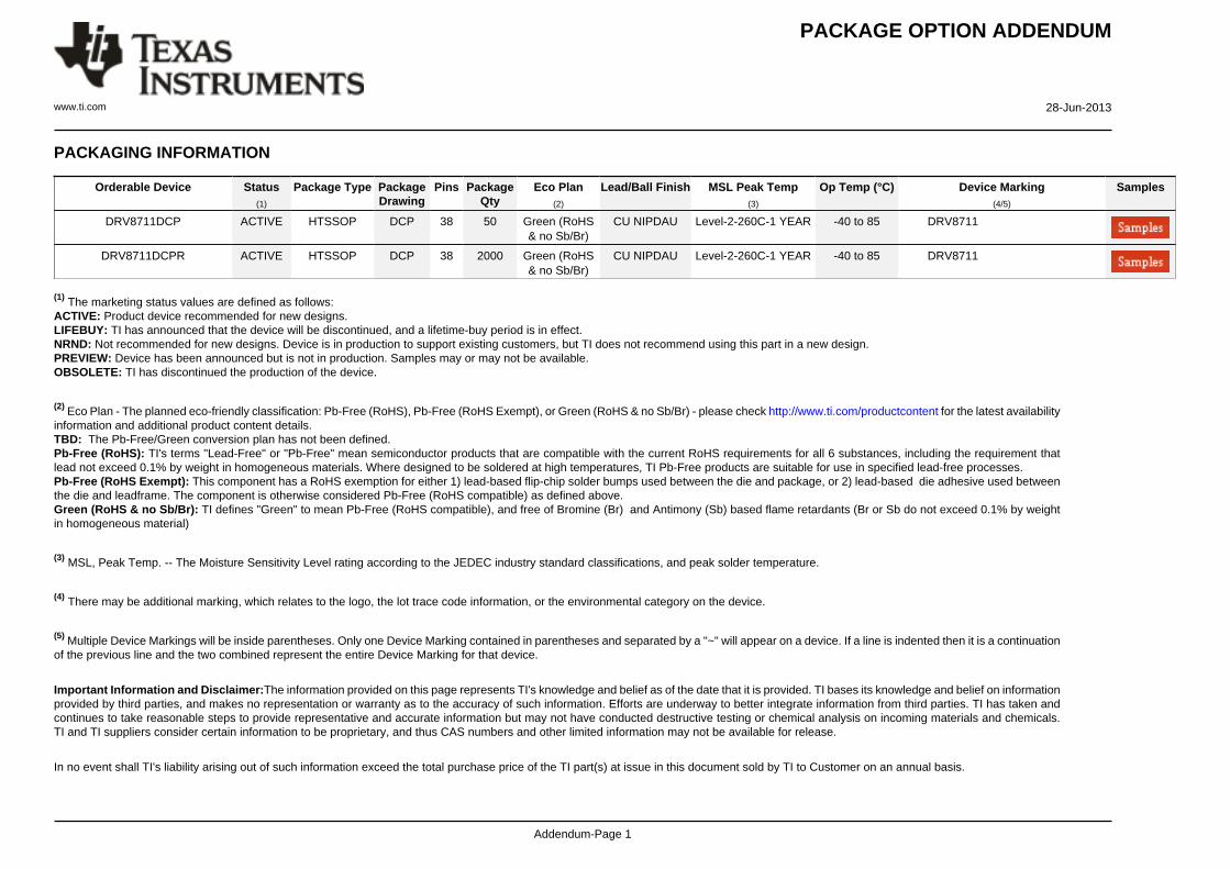
PACKAGE OPTION ADDENDUM
www.ti.com 28-Jun-2013
Addendum-Page 1
PACKAGING INFORMATION
Orderable Device Status(1)
Package Type PackageDrawing
Pins PackageQty
Eco Plan(2)
Lead/Ball Finish MSL Peak Temp(3)
Op Temp (°C) Device Marking(4/5)
Samples
DRV8711DCP ACTIVE HTSSOP DCP 38 50 Green (RoHS& no Sb/Br)
CU NIPDAU Level-2-260C-1 YEAR -40 to 85 DRV8711
DRV8711DCPR ACTIVE HTSSOP DCP 38 2000 Green (RoHS& no Sb/Br)
CU NIPDAU Level-2-260C-1 YEAR -40 to 85 DRV8711
(1) The marketing status values are defined as follows:ACTIVE: Product device recommended for new designs.LIFEBUY: TI has announced that the device will be discontinued, and a lifetime-buy period is in effect.NRND: Not recommended for new designs. Device is in production to support existing customers, but TI does not recommend using this part in a new design.PREVIEW: Device has been announced but is not in production. Samples may or may not be available.OBSOLETE: TI has discontinued the production of the device.
(2) Eco Plan - The planned eco-friendly classification: Pb-Free (RoHS), Pb-Free (RoHS Exempt), or Green (RoHS & no Sb/Br) - please check http://www.ti.com/productcontent for the latest availabilityinformation and additional product content details.TBD: The Pb-Free/Green conversion plan has not been defined.Pb-Free (RoHS): TI's terms "Lead-Free" or "Pb-Free" mean semiconductor products that are compatible with the current RoHS requirements for all 6 substances, including the requirement thatlead not exceed 0.1% by weight in homogeneous materials. Where designed to be soldered at high temperatures, TI Pb-Free products are suitable for use in specified lead-free processes.Pb-Free (RoHS Exempt): This component has a RoHS exemption for either 1) lead-based flip-chip solder bumps used between the die and package, or 2) lead-based die adhesive used betweenthe die and leadframe. The component is otherwise considered Pb-Free (RoHS compatible) as defined above.Green (RoHS & no Sb/Br): TI defines "Green" to mean Pb-Free (RoHS compatible), and free of Bromine (Br) and Antimony (Sb) based flame retardants (Br or Sb do not exceed 0.1% by weightin homogeneous material)
(3) MSL, Peak Temp. -- The Moisture Sensitivity Level rating according to the JEDEC industry standard classifications, and peak solder temperature.
(4) There may be additional marking, which relates to the logo, the lot trace code information, or the environmental category on the device.
(5) Multiple Device Markings will be inside parentheses. Only one Device Marking contained in parentheses and separated by a "~" will appear on a device. If a line is indented then it is a continuationof the previous line and the two combined represent the entire Device Marking for that device.
Important Information and Disclaimer:The information provided on this page represents TI's knowledge and belief as of the date that it is provided. TI bases its knowledge and belief on informationprovided by third parties, and makes no representation or warranty as to the accuracy of such information. Efforts are underway to better integrate information from third parties. TI has taken andcontinues to take reasonable steps to provide representative and accurate information but may not have conducted destructive testing or chemical analysis on incoming materials and chemicals.TI and TI suppliers consider certain information to be proprietary, and thus CAS numbers and other limited information may not be available for release.
In no event shall TI's liability arising out of such information exceed the total purchase price of the TI part(s) at issue in this document sold by TI to Customer on an annual basis.


IMPORTANT NOTICE
Texas Instruments Incorporated and its subsidiaries (TI) reserve the right to make corrections, enhancements, improvements and otherchanges to its semiconductor products and services per JESD46, latest issue, and to discontinue any product or service per JESD48, latestissue. Buyers should obtain the latest relevant information before placing orders and should verify that such information is current andcomplete. All semiconductor products (also referred to herein as “components”) are sold subject to TI’s terms and conditions of salesupplied at the time of order acknowledgment.
TI warrants performance of its components to the specifications applicable at the time of sale, in accordance with the warranty in TI’s termsand conditions of sale of semiconductor products. Testing and other quality control techniques are used to the extent TI deems necessaryto support this warranty. Except where mandated by applicable law, testing of all parameters of each component is not necessarilyperformed.
TI assumes no liability for applications assistance or the design of Buyers’ products. Buyers are responsible for their products andapplications using TI components. To minimize the risks associated with Buyers’ products and applications, Buyers should provideadequate design and operating safeguards.
TI does not warrant or represent that any license, either express or implied, is granted under any patent right, copyright, mask work right, orother intellectual property right relating to any combination, machine, or process in which TI components or services are used. Informationpublished by TI regarding third-party products or services does not constitute a license to use such products or services or a warranty orendorsement thereof. Use of such information may require a license from a third party under the patents or other intellectual property of thethird party, or a license from TI under the patents or other intellectual property of TI.
Reproduction of significant portions of TI information in TI data books or data sheets is permissible only if reproduction is without alterationand is accompanied by all associated warranties, conditions, limitations, and notices. TI is not responsible or liable for such altereddocumentation. Information of third parties may be subject to additional restrictions.
Resale of TI components or services with statements different from or beyond the parameters stated by TI for that component or servicevoids all express and any implied warranties for the associated TI component or service and is an unfair and deceptive business practice.TI is not responsible or liable for any such statements.
Buyer acknowledges and agrees that it is solely responsible for compliance with all legal, regulatory and safety-related requirementsconcerning its products, and any use of TI components in its applications, notwithstanding any applications-related information or supportthat may be provided by TI. Buyer represents and agrees that it has all the necessary expertise to create and implement safeguards whichanticipate dangerous consequences of failures, monitor failures and their consequences, lessen the likelihood of failures that might causeharm and take appropriate remedial actions. Buyer will fully indemnify TI and its representatives against any damages arising out of the useof any TI components in safety-critical applications.
In some cases, TI components may be promoted specifically to facilitate safety-related applications. With such components, TI’s goal is tohelp enable customers to design and create their own end-product solutions that meet applicable functional safety standards andrequirements. Nonetheless, such components are subject to these terms.
No TI components are authorized for use in FDA Class III (or similar life-critical medical equipment) unless authorized officers of the partieshave executed a special agreement specifically governing such use.
Only those TI components which TI has specifically designated as military grade or “enhanced plastic” are designed and intended for use inmilitary/aerospace applications or environments. Buyer acknowledges and agrees that any military or aerospace use of TI componentswhich have not been so designated is solely at the Buyer's risk, and that Buyer is solely responsible for compliance with all legal andregulatory requirements in connection with such use.
TI has specifically designated certain components as meeting ISO/TS16949 requirements, mainly for automotive use. In any case of use ofnon-designated products, TI will not be responsible for any failure to meet ISO/TS16949.
Products Applications
Audio www.ti.com/audio Automotive and Transportation www.ti.com/automotive
Amplifiers amplifier.ti.com Communications and Telecom www.ti.com/communications
Data Converters dataconverter.ti.com Computers and Peripherals www.ti.com/computers
DLP® Products www.dlp.com Consumer Electronics www.ti.com/consumer-apps
DSP dsp.ti.com Energy and Lighting www.ti.com/energy
Clocks and Timers www.ti.com/clocks Industrial www.ti.com/industrial
Interface interface.ti.com Medical www.ti.com/medical
Logic logic.ti.com Security www.ti.com/security
Power Mgmt power.ti.com Space, Avionics and Defense www.ti.com/space-avionics-defense
Microcontrollers microcontroller.ti.com Video and Imaging www.ti.com/video
RFID www.ti-rfid.com
OMAP Applications Processors www.ti.com/omap TI E2E Community e2e.ti.com
Wireless Connectivity www.ti.com/wirelessconnectivity
Mailing Address: Texas Instruments, Post Office Box 655303, Dallas, Texas 75265Copyright © 2013, Texas Instruments Incorporated

Mouser Electronics
Authorized Distributor
Click to View Pricing, Inventory, Delivery & Lifecycle Information: Texas Instruments:
DRV8711DCP DRV8711DCPR