DRV8701 Brushed DC Motor Full-Bridge Gate Driver (Rev. B) · PDF file5.9V to 45 V DRV8701...
43
5.9V to 45 V DRV8701 H-Bridge Gate Driver VREF PH/EN or PWM Controller Gate drive sense sense output nSLEEP Shunt Amp Protection FETs nFAULT M LDO 3.3 & 4.8 V 30 mA High-side VGS Low-side VGS High-side gate drive current Low-side gate drive current tDRIVE tDRIVE I DRIVE,SRC I DRIVE,SRC I DRIVE,SNK I DRIVE,SNK I STRONG I STRONG IHOLD IHOLD IHOLD IHOLD IHOLD IHOLD Product Folder Sample & Buy Technical Documents Tools & Software Support & Community DRV8701 SLVSCX5B – MARCH 2015 – REVISED JULY 2015 DRV8701 Brushed DC Motor Full-Bridge Gate Driver 1 Features 2 Applications 1• Single H-Bridge Gate Driver • Industrial Brushed-DC Motors • Robotics – Drives Four External N-Channel MOSFETs • Home Automation – Supports 100% PWM Duty Cycle • Industrial Pumps and Valves • 5.9-V to 45-V Operating Supply Voltage Range • Power Tools • Two Control Interface Options • Handheld Vacuum Cleaners – PH/EN (DRV8701E) – PWM (DRV8701P) 3 Description • Adjustable Gate Drive (5 Levels) The DRV8701 is a single H-bridge gate driver that – 6-mA to 150-mA Source Current uses four external N-channel MOSFETs targeted to – 12.5-mA to 300-mA Sink Current drive a 12-V to 24-V bidirectional brushed DC motor. • Supports 1.8-V, 3.3-V, and 5-V Logic Inputs A PH/EN (DRV8701E) or PWM (DRV8701P) • Current Shunt Amplifier (20 V/V) interface allows simple interfacing to controller circuits. An internal sense amplifier allows for • Integrated PWM Current Regulation adjustable current control. The gate driver includes – Limits Motor Inrush Current circuitry to regulate the winding current using fixed • Low-Power Sleep Mode (9 μA) off-time PWM current chopping. • Two LDO Voltage Regulators to Power External DRV8701 drives both high- and low-side FETs with Components 9.5-V V GS gate drive. The gate drive current for all – AVDD: 4.8 V, up to 30-mA Output Load external FETs is configurable with a single external resistor on the IDRIVE pin. – DVDD: 3.3 V, up to 30-mA Output Load A low-power sleep mode is provided which shuts • Small Package and Footprint down internal circuitry to achieve very-low quiescent – 24-Pin VQFN (PowerPAD™) current draw. This sleep mode can be set by taking – 4.0 × 4.0 × 0.9 mm the nSLEEP pin low. • Protection Features: Internal protection functions are provided: – VM Undervoltage Lockout (UVLO) undervoltage lockout, charge pump faults, overcurrent shutdown, short-circuit protection, – Charge Pump Undervoltage (CPUV) predriver faults, and overtemperature. Fault – Overcurrent Protection (OCP) conditions are indicated on the nFAULT pin. – Pre-Driver Fault (PDF) – Thermal Shutdown (TSD) Device Information (1) PART NUMBER PACKAGE BODY SIZE (NOM) – Fault Condition Output (nFAULT) DRV8701 VQFN (24) 4.00 × 4.00 x 0.90 mm (1) For all available packages, see the orderable addendum at the end of the data sheet. SPACE Gate-Drive Current Simplified System Block Diagram 1 An IMPORTANT NOTICE at the end of this data sheet addresses availability, warranty, changes, use in safety-critical applications, intellectual property matters and other important disclaimers. PRODUCTION DATA.
Transcript of DRV8701 Brushed DC Motor Full-Bridge Gate Driver (Rev. B) · PDF file5.9V to 45 V DRV8701...
5.9V to 45 V
DRV8701
H-Bridge Gate
DriverVREF
PH/EN or PWM
Controller
Gate drive
sensesense output
nSLEEP
Shunt Amp
Protection
FETs
nFAULT
M
LDO 3.3 & 4.8 V30 mA
High-side VGS
Low-side VGS
High-side gate drive
current
Low-side gate drive
current
tDRIVE
tDRIVE
IDR
IVE
,SR
C
IDR
IVE
,SR
C
IDR
IVE
,SN
K
IDR
IVE
,SN
K
IST
RO
NG
IST
RO
NG
IHOLD
IHOLD
IHOLD
IHOLD
IHOLD
IHOLD
Product
Folder
Sample &Buy
Technical
Documents
Tools &
Software
Support &Community
DRV8701SLVSCX5B –MARCH 2015–REVISED JULY 2015
DRV8701 Brushed DC Motor Full-Bridge Gate Driver1 Features 2 Applications1• Single H-Bridge Gate Driver • Industrial Brushed-DC Motors
• Robotics– Drives Four External N-Channel MOSFETs• Home Automation– Supports 100% PWM Duty Cycle• Industrial Pumps and Valves• 5.9-V to 45-V Operating Supply Voltage Range• Power Tools• Two Control Interface Options• Handheld Vacuum Cleaners– PH/EN (DRV8701E)
– PWM (DRV8701P)3 Description• Adjustable Gate Drive (5 Levels)The DRV8701 is a single H-bridge gate driver that– 6-mA to 150-mA Source Current uses four external N-channel MOSFETs targeted to
– 12.5-mA to 300-mA Sink Current drive a 12-V to 24-V bidirectional brushed DC motor.• Supports 1.8-V, 3.3-V, and 5-V Logic Inputs A PH/EN (DRV8701E) or PWM (DRV8701P)• Current Shunt Amplifier (20 V/V) interface allows simple interfacing to controller
circuits. An internal sense amplifier allows for• Integrated PWM Current Regulationadjustable current control. The gate driver includes– Limits Motor Inrush Current circuitry to regulate the winding current using fixed
• Low-Power Sleep Mode (9 μA) off-time PWM current chopping.• Two LDO Voltage Regulators to Power External DRV8701 drives both high- and low-side FETs with
Components 9.5-V VGS gate drive. The gate drive current for all– AVDD: 4.8 V, up to 30-mA Output Load external FETs is configurable with a single external
resistor on the IDRIVE pin.– DVDD: 3.3 V, up to 30-mA Output LoadA low-power sleep mode is provided which shuts• Small Package and Footprintdown internal circuitry to achieve very-low quiescent– 24-Pin VQFN (PowerPAD™)current draw. This sleep mode can be set by taking
– 4.0 × 4.0 × 0.9 mm the nSLEEP pin low.• Protection Features: Internal protection functions are provided:
– VM Undervoltage Lockout (UVLO) undervoltage lockout, charge pump faults,overcurrent shutdown, short-circuit protection,– Charge Pump Undervoltage (CPUV)predriver faults, and overtemperature. Fault– Overcurrent Protection (OCP)conditions are indicated on the nFAULT pin.
– Pre-Driver Fault (PDF)– Thermal Shutdown (TSD) Device Information(1)
PART NUMBER PACKAGE BODY SIZE (NOM)– Fault Condition Output (nFAULT)DRV8701 VQFN (24) 4.00 × 4.00 x 0.90 mm
(1) For all available packages, see the orderable addendum atthe end of the data sheet.
SPACE Gate-Drive Current
Simplified System Block Diagram
1
An IMPORTANT NOTICE at the end of this data sheet addresses availability, warranty, changes, use in safety-critical applications,intellectual property matters and other important disclaimers. PRODUCTION DATA.

DRV8701SLVSCX5B –MARCH 2015–REVISED JULY 2015 www.ti.com
Table of Contents7.4 Device Functional Modes........................................ 261 Features .................................................................. 1
8 Application and Implementation ........................ 282 Applications ........................................................... 18.1 Application Information............................................ 283 Description ............................................................. 18.2 Typical Applications ............................................... 284 Revision History..................................................... 2
9 Power Supply Recommendations ...................... 325 Pin Configuration and Functions ......................... 39.1 Bulk Capacitance Sizing ......................................... 326 Specifications......................................................... 5
10 Layout................................................................... 336.1 Absolute Maximum Ratings ...................................... 510.1 Layout Guidelines ................................................. 336.2 ESD Ratings.............................................................. 510.2 Layout Example .................................................... 336.3 Recommended Operating Conditions....................... 5
11 Device and Documentation Support ................. 346.4 Thermal Information .................................................. 611.1 Documentation Support ........................................ 346.5 Electrical Characteristics........................................... 711.2 Community Resources.......................................... 346.6 Typical Characteristics .............................................. 911.3 Trademarks ........................................................... 347 Detailed Description ............................................ 1211.4 Electrostatic Discharge Caution............................ 347.1 Overview ................................................................. 1211.5 Glossary ................................................................ 347.2 Functional Block Diagram ....................................... 13
12 Mechanical, Packaging, and Orderable7.3 Feature Description................................................. 14Information ........................................................... 34
4 Revision HistoryNOTE: Page numbers for previous revisions may differ from page numbers in the current version.
Changes from Revision A (May 2015) to Revision B Page
• Updated test conditions for IDRIVE,SNK and corrected TYP values ........................................................................................... 8
Changes from Original (March 2015) to Revision A Page
• Updated device status to production data ............................................................................................................................. 1
2 Submit Documentation Feedback Copyright © 2015, Texas Instruments Incorporated
Product Folder Links: DRV8701
1
2
3
4
5
6
18
17
16
15
14
13
24
23
22
21
20
7 8 9 10
11
12
VM
VCP
CPH
CPL
GND
VREF
SH1
GH1
GND
PH
EN
nSLEEP
AVDD
DVDD
nFAULT
SNSOUT
SO
IDRIVE
GL1
SN
SP
GL2
SH2
GH2
GND(PPAD)
19
1
2
3
4
5
6
18
17
16
15
14
13
24
23
22
21
20
7 8 9 10
11
12
VM
VCP
CPH
CPL
GND
VREF
SH1
GH1
GND
IN1
IN2
nSLEEP
AVDD
DVDD
nFAULT
SNSOUT
SO
IDRIVE
GL1
SN
SP
GL2
SH2
GH2
GND(PPAD)
19
DRV8701www.ti.com SLVSCX5B –MARCH 2015–REVISED JULY 2015
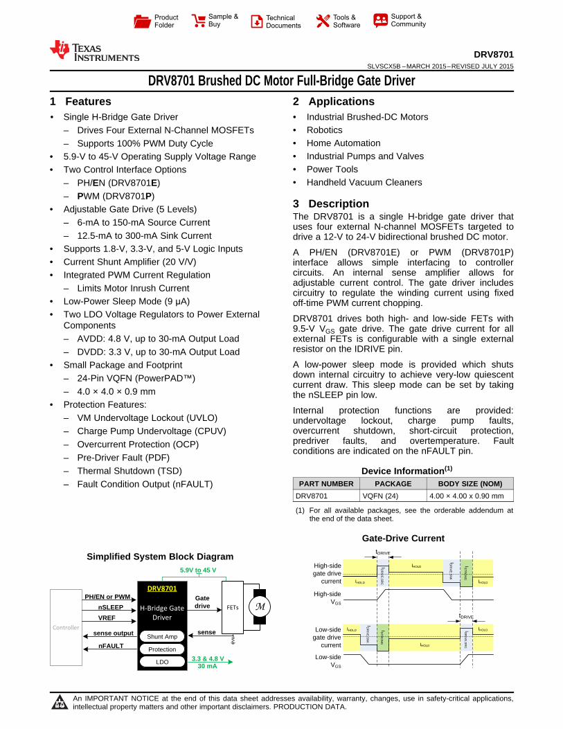
5 Pin Configuration and Functions
RGE Package RGE Package24-Pin VQFN 24-Pin VQFN
DRV8701E Top View DRV8701P Top View
DRV8701E (PH/EN)PIN
TYPE DESCRIPTIONNAME NO.
EN 14 Input Bridge enable input Logic low places the bridge in brake mode; see Table 1PH 15 Input Bridge phase input Controls the direction of the H-bridge; see Table 1
DRV8701P (PWM)PIN
TYPE DESCRIPTIONNAME NO.
IN1 15 InputBridge PWM input Logic controls the state of H-bridge; see Table 2
IN2 14 Input
Common PinsPIN
TYPE DESCRIPTIONNAME NO.
Connect to motor supply voltage; bypass to GND with a 0.1-µFVM 1 Power Power supply ceramic plus a 10-µF minimum capacitor rated for VM; additional
capacitance may be required based on drive current5
GND 16 Power Device ground Must be connected to groundPPAD
VCP 2 Power Charge pump output Connect a 16-V, 1-µF ceramic capacitor to VMCPH 3 Connect a 0.1-µF X7R capacitor rated for VM between CPH andPower Charge pump switching nodes CPLCPL 4
3.3-V logic supply regulator; bypass to GND with a 6.3-V, 1-µFDVDD 8 Power Logic regulator ceramic capacitor4.8-V analog supply regulator; bypass to GND with a 6.3-V, 1-µFAVDD 7 Power Analog regulator ceramic capacitorPull logic low to put device into a low-power sleep mode with FETsnSLEEP 13 Input Device sleep mode High-Z; internal pulldownResistor value or voltage forced on this pin sets the gate driveIDRIVE 12 Input Gate drive current setting pin current; see applications section for more details
Copyright © 2015, Texas Instruments Incorporated Submit Documentation Feedback 3
Product Folder Links: DRV8701
DRV8701SLVSCX5B –MARCH 2015–REVISED JULY 2015 www.ti.com
Common Pins (continued)PIN
TYPE DESCRIPTIONNAME NO.
Controls the current regulation; apply a voltage between 0.3 V andVREF 6 Input Analog reference input AVDDOpen Pulled logic low with fault condition; open-drain output requires annFAULT 9 Fault indication pinDrain external pullupOpen Pulled logic low when the drive current hits the current choppingSNSOUT 10 Sense comparator outputDrain threshold; open-drain output requires an external pullup
Voltage on this pin is equal to the SP voltage times AV plus anSO 11 Output Shunt amplifier output offset; place no more than 1 nF of capacitance on this pinSN 20 Input Shunt amplifier negative input Connect to SP through current sense resistor and to GND
Connect to low-side FET source and to SN through current senseSP 21 Input Shunt amplifier positive input resistorGH1 17
Output High-side gate Connect to high-side FET gateGH2 24GL1 19
Output Low-side gate Connect to low-side FET gateGL2 22SH1 18
Input Phase node Connect to high-side FET source and low-side FET drainSH2 23
External Passive ComponentsCOMPONENT PIN 1 PIN 2 RECOMMENDED
CVM1 VM GND 0.1-µF ceramic capacitor rated for VMCVM2 VM GND ≥10-µF capacitor rated for VMCVCP VCP VM 16-V, 1-µF ceramic capacitorCSW CPH CPL 0.1-µF X7R capacitor rated for VMCDVDD DVDD GND 6.3-V, 1-µF ceramic capacitorCAVDD AVDD GND 6.3-V, 1-µF ceramic capacitorRIDRIVE IDRIVE GND See Typical Applications for resistor sizingRnFAULT VCC (1) nFAULT ≥10-kΩ pullupRSNSOUT VCC (1) SNSOUT ≥10-kΩ pullupRSENSE SP SN/GND Optional low-side sense resistor
(1) VCC is not a pin on the DRV8701, but a VCC supply voltage pullup is required for open-drain outputs nFAULT and SNSOUT. Thesystem controller supply can be used for this pullup voltage, or these pins can be pulled up to either AVDD or DVDD.
External FETsComponent Gate Drain Source Recommended
QHS1 GH1 VM SH1QLS1 GL1 SH1 SP or GND Supports up to 200-nC FETs at 40-kHz PWM; see
Detailed Design Procedure for more detailsQHS2 GH2 VM SH2QLS2 GL2 SH2 SP or GND
4 Submit Documentation Feedback Copyright © 2015, Texas Instruments Incorporated
Product Folder Links: DRV8701

DRV8701www.ti.com SLVSCX5B –MARCH 2015–REVISED JULY 2015
6 Specifications
6.1 Absolute Maximum Ratingsover operating free-air temperature range referenced with respect to GND (unless otherwise noted) (1)
MIN MAX UNITPower supply voltage (VM) –0.3 47 VPower supply voltage ramp rate (VM) 0 2 V/µsCharge pump voltage (VCP, CPH) –0.3 VM + 12 VCharge pump negative switching pin (CPL) –0.3 VM VInternal logic regulator voltage (DVDD) –0.3 3.8 VInternal analog regulator voltage (AVDD) –0.3 5.75 VControl pin voltage (PH, EN, IN1, IN2, nSLEEP, nFAULT, VREF, IDRIVE, SNSOUT) –0.3 5.75 VHigh-side gate pin voltage (GH1, GH2) –0.3 VM + 12 VContinuous phase node pin voltage (SH1, SH2) –1.2 VM + 1.2 VPulsed 10 µs phase node pin voltage (SH1, SH2) –2.0 VM + 2 VLow-side gate pin voltage (GL1, GL2) –0.3 12 VContinuous shunt amplifier input pin voltage (SP, SN) –0.5 1 VPulsed 10-µs shunt amplifier input pin voltage (SP, SN) –1 1 VShunt amplifier output pin voltage (SO) –0.3 5.75 VOpen-drain output current (nFAULT, SNSOUT) 0 10 mAGate pin source current (GH1, GL1, GH2, GL2) 0 250 mAGate pin sink current (GH1, GL1, GH2, GL2) 0 500 mAShunt amplifier output pin current (SO) 0 5 mAOperating junction temperature, TJ –40 150 °CStorage temperature, Tstg –65 150 °C
(1) Stresses beyond those listed under Absolute Maximum Ratings may cause permanent damage to the device. These are stress ratingsonly, which do not imply functional operation of the device at these or any other conditions beyond those indicated under RecommendedOperating Conditions. Exposure to absolute-maximum-rated conditions for extended periods may affect device reliability.
6.2 ESD RatingsVALUE UNIT
Human body model (HBM) ESD stress voltage (1) ±2000V(ESD) Electrostatic discharge V
Charged device model (CDM) ESD stress voltage (2) ±500
(1) JEDEC document JEP155 states that 500-V HBM allows safe manufacturing with a standard ESD control process.(2) JEDEC document JEP157 states that 250-V CDM allows safe manufacturing with a standard ESD control process.
6.3 Recommended Operating Conditionsover operating free-air temperature range (unless otherwise noted)
MIN MAX UNITVM Power supply voltage range 5.9 45 VVCC Logic level input voltage 0 5.5 VVREF Reference RMS voltage range (VREF) 0.3 (1) AVDD VƒPWM Applied PWM signal (PH/EN or IN1/IN2) 100 kHzIAVDD AVDD external load current 30 (2) mAIDVDD DVDD external load current 30 (2) mAISO Shunt amplifier output current loading (SO) 5 mATA Operating ambient temperature –40 125 °C
(1) Operational at VREF = 0 to 0.3 V, but accuracy is degraded(2) Power dissipation and thermal limits must be observed
Copyright © 2015, Texas Instruments Incorporated Submit Documentation Feedback 5
Product Folder Links: DRV8701

DRV8701SLVSCX5B –MARCH 2015–REVISED JULY 2015 www.ti.com
6.4 Thermal InformationDRV8701
THERMAL METRIC (1) RGE (VQFN) UNIT24 PINS
RθJA Junction-to-ambient thermal resistance 34.8 °C/WRθJC(top) Junction-to-case (top) thermal resistance 37.1 °C/WRθJB Junction-to-board thermal resistance 12.2 °C/WψJT Junction-to-top characterization parameter 0.6 °C/WψJB Junction-to-board characterization parameter 12.2 °C/WRθJC(bot) Junction-to-case (bottom) thermal resistance 3.7 °C/W
(1) For more information about traditional and new thermal metrics, see the Semiconductor and IC Package Thermal Metrics applicationreport, SPRA953.
6 Submit Documentation Feedback Copyright © 2015, Texas Instruments Incorporated
Product Folder Links: DRV8701

DRV8701www.ti.com SLVSCX5B –MARCH 2015–REVISED JULY 2015
6.5 Electrical Characteristicsover operating free-air temperature range (unless otherwise noted)
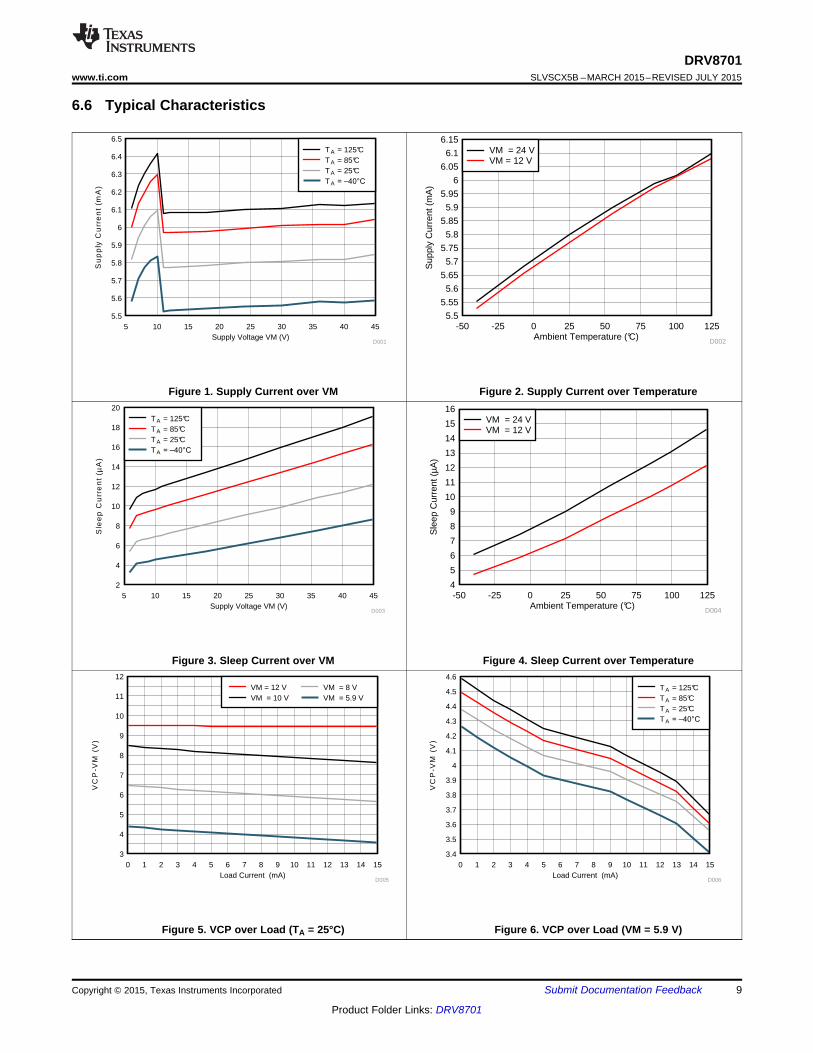
PARAMETER TEST CONDITIONS MIN TYP MAX UNITPOWER SUPPLIES (VM, AVDD, DVDD)VM VM operating voltage 5.9 45 VIVM VM operating supply current VM = 24 V; nSLEEP high 6 9.5 mA
TA = 25°C 9 15nSLEEP = 0IVMQ VM sleep mode supply current μAVM = 24 V TA = 125°C (1) 14 25tSLEEP Sleep time nSLEEP low to sleep mode 100 μstWAKE Wake-up time nSLEEP high to output change 1 mstON Turn-on time VM > UVLO to output transition 1 msDVDD Internal logic regulator voltage External load 0 to 30 mA 3.0 3.3 3.5 VAVDD Internal logic regulator voltage External load 0 to 30 mA 4.4 4.8 5.2 VCHARGE PUMP (VCP, CPH, CPL)
VM = 12 V; IVCP = 0 to 12 mA 20.5 21.5 22.5VCP VCP operating voltage VM = 8 V; IVCP = 0 to 10 mA 13.5 14.4 15 V
VM = 5.9 V; IVCP = 0 to 8 mA 9.4 9.9 10.4VM > 12 V 12
IVCP Charge pump current capacity 8 V < VM < 12 V 10 mA5.9 V < VM < 8 V 8
fVCP(1) Charge pump switching frequency VM > UVLO 200 400 700 kHz
CONTROL INPUTS (PH, EN, IN1, IN2, nSLEEP)VIL Input logic low voltage 0.8 VVIH Input logic high voltage 1.5 VVHYS Input logic hysteresis 100 mVIIL Input logic low current VIN = 0 V –5 5 μAIIH Input logic high current VIN = 5 V 78 μARPD Pulldown resistance 64 115 173 kΩtPD Propagation delay PH/EN, IN1/IN2 to GHx/GLx 500 nsCONTROL OUTPUTS (nFAULT, SNSOUT)VOL Output logic low voltage IO = 2 mA 0.1 VIOZ Output high impedance leakage VIN = 5 V –2 2 μAFET GATE DRIVERS (GH1, GH2, SH1, SH2, GL1, GL2)
VM > 12 V; VGHS with respect to SHx 8.5 9.5 10.5High-side VGS gate drive (gate-to-VGHS VM = 8 V; VGHS with respect to SHx 5.5 6.4 7 Vsource)
VM = 5.9 V; VGHS with respect to SHx 3.5 4.0 4.5VM > 12 V 8.5 9.3 10.5Low-side VGS gate drive (gate-to-VGLS Vsource) VM = 5.9 V 3.9 4.3 4.9Observed tDEAD depends on IDRIVEtDEAD Output dead time 380 nssetting
tDRIVE Gate drive time 2.5 μsRIDRIVE < 1 kΩ to GND 6RIDRIVE = 33 kΩ ±5% to GND 12.5RIDRIVE = 200 kΩ ±5% to GND, orIDRIVE,SRC Peak source current 25 mARIDRIVE < 1 kΩ to AVDDRIDRIVE > 500 kΩ ±5% to GND 100RIDRIVE = 68 kΩ ±5% to AVDD 150
(1) Specified by design and characterization data
Copyright © 2015, Texas Instruments Incorporated Submit Documentation Feedback 7
Product Folder Links: DRV8701
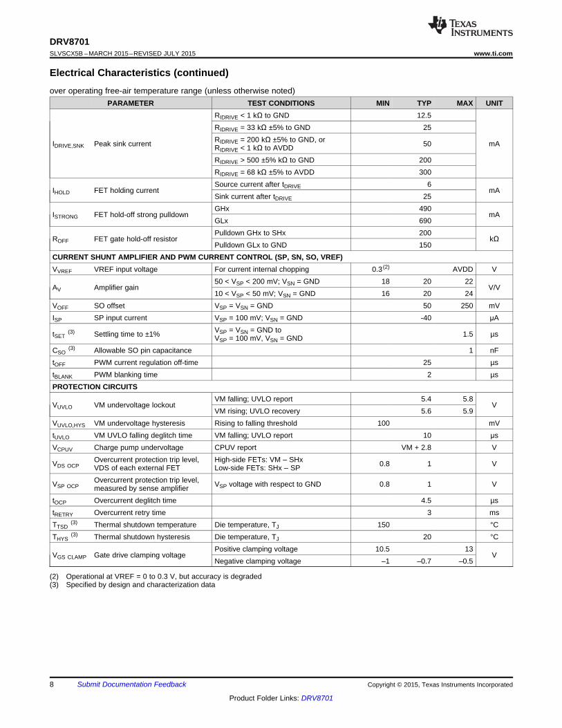
DRV8701SLVSCX5B –MARCH 2015–REVISED JULY 2015 www.ti.com
Electrical Characteristics (continued)over operating free-air temperature range (unless otherwise noted)
PARAMETER TEST CONDITIONS MIN TYP MAX UNITRIDRIVE < 1 kΩ to GND 12.5RIDRIVE = 33 kΩ ±5% to GND 25RIDRIVE = 200 kΩ ±5% to GND, orIDRIVE,SNK Peak sink current 50 mARIDRIVE < 1 kΩ to AVDDRIDRIVE > 500 ±5% kΩ to GND 200RIDRIVE = 68 kΩ ±5% to AVDD 300Source current after tDRIVE 6
IHOLD FET holding current mASink current after tDRIVE 25GHx 490
ISTRONG FET hold-off strong pulldown mAGLx 690Pulldown GHx to SHx 200
ROFF FET gate hold-off resistor kΩPulldown GLx to GND 150
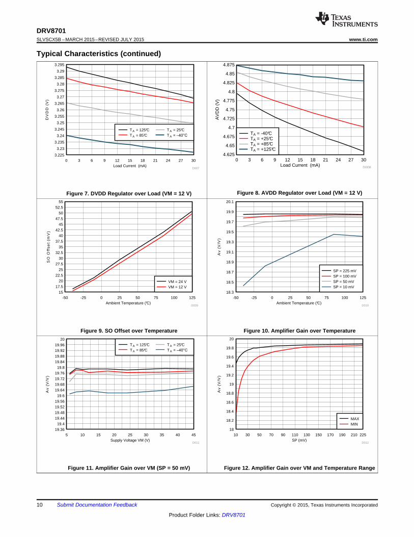
CURRENT SHUNT AMPLIFIER AND PWM CURRENT CONTROL (SP, SN, SO, VREF)VVREF VREF input voltage For current internal chopping 0.3 (2) AVDD V
50 < VSP < 200 mV; VSN = GND 18 20 22AV Amplifier gain V/V
10 < VSP < 50 mV; VSN = GND 16 20 24VOFF SO offset VSP = VSN = GND 50 250 mVISP SP input current VSP = 100 mV; VSN = GND -40 μA
VSP = VSN = GND totSET(3) Settling time to ±1% 1.5 µsVSP = 100 mV, VSN = GND
CSO(3) Allowable SO pin capacitance 1 nF
tOFF PWM current regulation off-time 25 µstBLANK PWM blanking time 2 µsPROTECTION CIRCUITS
VM falling; UVLO report 5.4 5.8VUVLO VM undervoltage lockout V
VM rising; UVLO recovery 5.6 5.9VUVLO,HYS VM undervoltage hysteresis Rising to falling threshold 100 mVtUVLO VM UVLO falling deglitch time VM falling; UVLO report 10 μsVCPUV Charge pump undervoltage CPUV report VM + 2.8 V
Overcurrent protection trip level, High-side FETs: VM – SHxVDS OCP 0.8 1 VVDS of each external FET Low-side FETs: SHx – SPOvercurrent protection trip level,VSP OCP VSP voltage with respect to GND 0.8 1 Vmeasured by sense amplifier
tOCP Overcurrent deglitch time 4.5 µstRETRY Overcurrent retry time 3 msTTSD
(3) Thermal shutdown temperature Die temperature, TJ 150 °CTHYS
(3) Thermal shutdown hysteresis Die temperature, TJ 20 °CPositive clamping voltage 10.5 13
VGS CLAMP Gate drive clamping voltage VNegative clamping voltage –1 –0.7 –0.5
(2) Operational at VREF = 0 to 0.3 V, but accuracy is degraded(3) Specified by design and characterization data
8 Submit Documentation Feedback Copyright © 2015, Texas Instruments Incorporated
Product Folder Links: DRV8701
Load Current (mA)
VC
P-V
M (
V)
0 1 2 3 4 5 6 7 8 9 10 11 12 13 14 153
4
5
6
7
8
9
10
11
12
D005
VM = 12 VVM = 10 V
VM = 8 VVM = 5.9 V
Load Current (mA)
VC
P-V
M (
V)
0 1 2 3 4 5 6 7 8 9 10 11 12 13 14 153.4
3.5
3.6
3.7
3.8
3.9
4
4.1
4.2
4.3
4.4
4.5
4.6
D006
TA = 125°CTA = 85°CTA = 25°CTA ±&
Supply Voltage VM (V)
Sle
ep
Cu
rre
nt
(µA
)
5 10 15 20 25 30 35 40 452
4
6
8
10
12
14
16
18
20
D003
TA = 125°CTA = 85°CTA = 25°CTA ±&
Ambient Temperature (°C)
Sle
ep C
urre
nt (
µA
)
-50 -25 0 25 50 75 100 1254
5
6
7
8
9
10
11
12
13
14
15
16
D004
VM = 24 VVM = 12 V
Supply Voltage VM (V)
Su
pp
ly C
urr
en
t (m
A)
5 10 15 20 25 30 35 40 455.5
5.6
5.7
5.8
5.9
6
6.1
6.2
6.3
6.4
6.5
D001
TA = 125°CTA = 85°CTA = 25°CTA ±&
Ambient Temperature (°C)
Sup
ply
Cur
rent
(m
A)
-50 -25 0 25 50 75 100 1255.5
5.55
5.6
5.65
5.7
5.75
5.8
5.85
5.9
5.95
6
6.05
6.1
6.15
D002
VM = 24 VVM = 12 V
DRV8701www.ti.com SLVSCX5B –MARCH 2015–REVISED JULY 2015
6.6 Typical Characteristics
Figure 1. Supply Current over VM Figure 2. Supply Current over Temperature
Figure 3. Sleep Current over VM Figure 4. Sleep Current over Temperature
Figure 5. VCP over Load (TA = 25°C) Figure 6. VCP over Load (VM = 5.9 V)
Copyright © 2015, Texas Instruments Incorporated Submit Documentation Feedback 9
Product Folder Links: DRV8701
Supply Voltage VM (V)
Av
(V
/V)
5 10 15 20 25 30 35 40 4519.36
19.4
19.44
19.48
19.52
19.56
19.6
19.64
19.68
19.72
19.7619.8
19.84
19.88
19.9219.96
20
D011
T A = 125°CT A = 85°C
T A = 25°CT A ±&
SP (mV)
Av
(V
/V)
10 30 50 70 90 110 130 150 170 190 210 22518
18.2
18.4
18.6
18.8
19
19.2
19.4
19.6
19.8
20
D012
MAXMIN
Ambient Temperature (°C)
SO
Off
se
t (m
V)
-50 -25 0 25 50 75 100 12515
17.5
20
22.5
25
27.5
30
32.5
35
37.5
40
42.5
45
47.5
5052.5
55
D009
VM = 24 VVM = 12 V
Ambient Temperature (°C)
Av
(V
/V)
-50 -25 0 25 50 75 100 12518.3
18.5
18.7
18.9
19.1
19.3
19.5
19.7
19.9
20.1
D010
SP = 225 mVSP = 100 mVSP = 50 mVSP = 10 mV
Load Current (mA)
DV
DD
(V
)
0 3 6 9 12 15 18 21 24 27 303.225
3.23
3.235
3.24
3.245
3.25
3.255
3.26
3.265
3.27
3.275
3.28
3.285
3.29
3.295
D007
T A = 125°CT A = 85°C
T A = 25°CT A ±&
Load Current (mA)
AV
DD
(V
)
0 3 6 9 12 15 18 21 24 27 304.625
4.65
4.675
4.7
4.725
4.75
4.775
4.8
4.825
4.85
4.875
D008
TA = -40°CTA = +25°CTA = +85°CTA = +125°C
DRV8701SLVSCX5B –MARCH 2015–REVISED JULY 2015 www.ti.com
Typical Characteristics (continued)
Figure 8. AVDD Regulator over Load (VM = 12 V)Figure 7. DVDD Regulator over Load (VM = 12 V)
Figure 9. SO Offset over Temperature Figure 10. Amplifier Gain over Temperature
Figure 11. Amplifier Gain over VM (SP = 50 mV) Figure 12. Amplifier Gain over VM and Temperature Range
10 Submit Documentation Feedback Copyright © 2015, Texas Instruments Incorporated
Product Folder Links: DRV8701

Supply Voltage VM (V)
Hig
h-S
ide
ID
RIV
EP
(m
A)
5 10 15 20 25 30 35 40 4590
95
100
105
110
115
120
125
130
D017
TA ±&
TA = 25°CTA = 85°CTA = 125°C
Supply Voltage VM (V)
Hig
h-S
ide
ID
RIV
EP
(m
A)
5 10 15 20 25 30 35 40 45130
135
140
145
150
155
160
165
170
175
180
185
D018
TA ±&
TA = 25°CTA = 85°CTA = 125°C
Supply Voltage VM (V)
Hig
h-S
ide
ID
RIV
EP
(m
A)
5 10 15 20 25 30 35 40 4512
12.5
13
13.5
14
14.5
15
15.5
16
D015
TA ±&
TA = 25°CTA = 85°CTA = 125°C
Supply Voltage VM (V)
Hig
h-S
ide
ID
RIV
EP
(m
A)
5 10 15 20 25 30 35 40 4524
25
26
27
28
29
30
31
32
33
D016
TA ±&
TA = 25°CTA = 85°CTA = 125°C
Ambient Temperature (°C)
Hig
h-S
ide
ID
RIV
EP
(m
A)
-50 -25 0 25 50 75 100 1250
20
40
60
80
100
120
140
160
180
D013
150/300 mA100/200 mA25/50 mA
12.5/25 mA6/12.5 mA
Supply Voltage VM (V)
Hig
h-S
ide
ID
RIV
EP
(m
A)
5 10 15 20 25 30 35 40 454.8
5
5.2
5.4
5.6
5.8
6
6.2
D014
TA ±&
TA = 25°CTA = 85°CTA = 125°C
DRV8701www.ti.com SLVSCX5B –MARCH 2015–REVISED JULY 2015
Typical Characteristics (continued)
Figure 13. High-Side IDRIVEP over Temperature (VM = 12 V) Figure 14. 6-/12.5-mA High-Side IDRIVEP over VM
Figure 15. 12.5-/25-mA High-Side IDRIVEP over VM Figure 16. 25-/50-mA High-Side IDRIVEP over VM
Figure 17. 100-/200-mA High-Side IDRIVEP over VM Figure 18. 150-/300-mA High-Side IDRIVEP over VM
Copyright © 2015, Texas Instruments Incorporated Submit Documentation Feedback 11
Product Folder Links: DRV8701

DRV8701SLVSCX5B –MARCH 2015–REVISED JULY 2015 www.ti.com
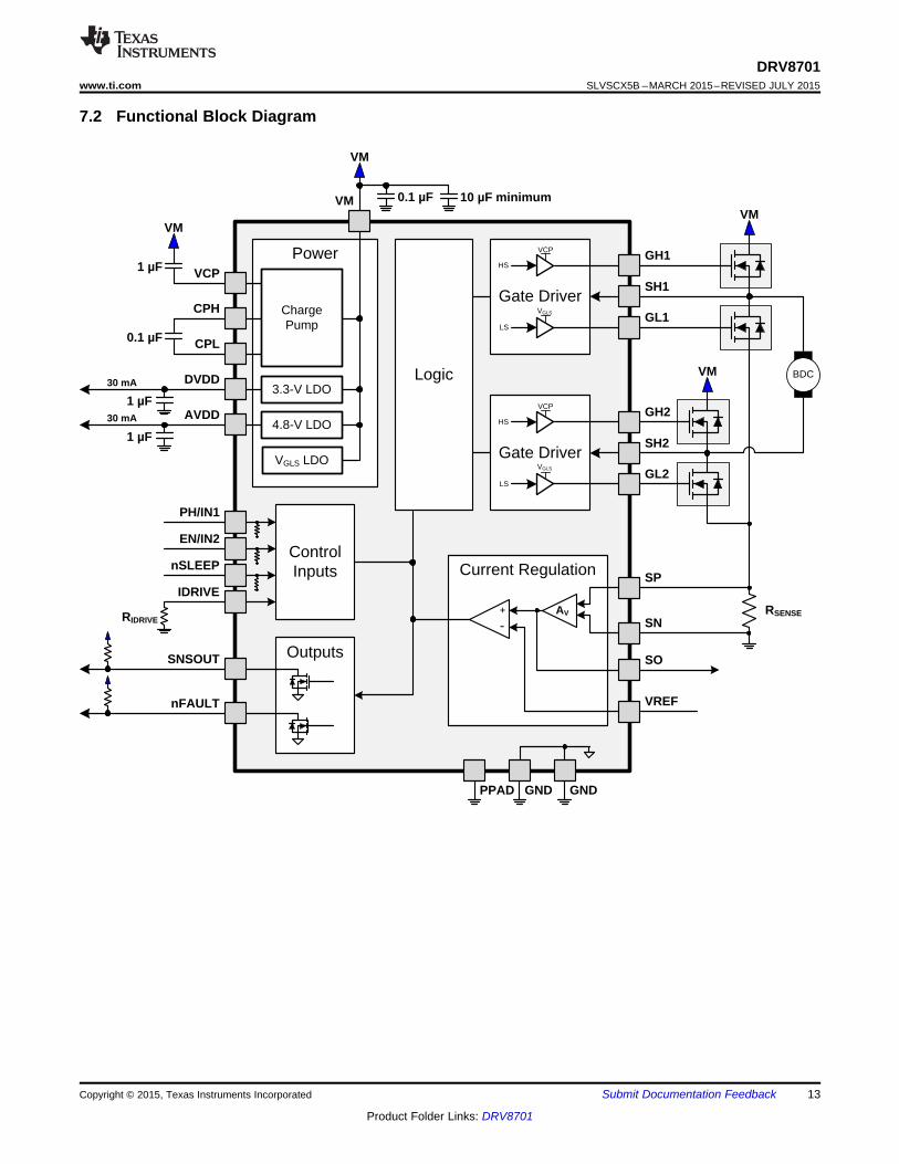
7 Detailed Description
7.1 OverviewThe DRV8701 is an H-bridge gate driver (also called a pre-driver or controller). The device integrates FET gatedrivers in order to control four external NMOS FETs. The device can be powered with a supply voltage between5.9 and 45 V.
A simple PH/EN (DRV8701E) or PWM (DRV8701P) interface allows interfacing to the controller circuit.
A low-power sleep mode is included, which can be enabled using the nSLEEP pin.
The gate drive strength can be adjusted to optimize a system for a given FET without adding external resistors inseries with the FET gates. The IDRIVE pin allows for selection of the peak current driven into the external FETgate. Both the high-side and low-side FETs are driven with a VGS of 9.5 V nominally when VM > 12 V. At lowerVM voltages, the VGS is reduced. The high-side gate drive voltage is generated using a doubler-architecturecharge pump that regulates to VM + 9.5 V.
This device greatly reduces the component count of discrete motor driver systems by integrating the necessaryFET drive circuitry into a single device. In addition, the DRV8701 adds protection features above traditionaldiscrete implementations: UVLO, OCP, pre-driver faults, and thermal shutdown.
A start-up (inrush) or running current limitation is built in using a fixed time-off current chopping scheme. Thechopping current level is set by choosing the sense resistor value and by setting a voltage on the VREF pin.
A shunt amplifier output is provided for accurate current measurements by the system controller. The SO pinoutputs a voltage that is 20 times the voltage seen across the sense resistor.
12 Submit Documentation Feedback Copyright © 2015, Texas Instruments Incorporated
Product Folder Links: DRV8701
Gate Driver
Gate Driver
Current Regulation
VM
VM
0.1 µF 10 µF minimum
PowerVCP
CPH
CPL
3.3-V LDO
4.8-V LDO
VGLS LDO
DVDD
AVDD
0.1 µF
Charge Pump
1 µF
VM
1 µF
1 µF
30 mA
30 mA
Control Inputs
PH/IN1
EN/IN2
nSLEEP
IDRIVE
RIDRIVE
OutputsSNSOUT
nFAULT
GL2
SH2
GH2VCP
VGLS
HS
LS
GL1
SH1
GH1VCP
VGLS
HS
LS
VM
VM
RSENSE+
-
AV
SP
SN
SO
VREF
GND
GND
PPAD
Logic BDC
DRV8701www.ti.com SLVSCX5B –MARCH 2015–REVISED JULY 2015
7.2 Functional Block Diagram
Copyright © 2015, Texas Instruments Incorporated Submit Documentation Feedback 13
Product Folder Links: DRV8701
SH1 SH22
1
22
Forward drive
Slow decay (brake)
VM
1
SH1 SH22
1
22
Reverse drive
Slow decay (brake)
VM
1
33 High-Z (coast) 3 High-Z (coast)
3
DRV8701SLVSCX5B –MARCH 2015–REVISED JULY 2015 www.ti.com
7.3 Feature Description
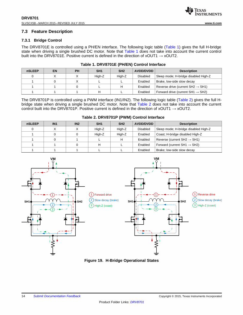
7.3.1 Bridge ControlThe DRV8701E is controlled using a PH/EN interface. The following logic table (Table 1) gives the full H-bridgestate when driving a single brushed DC motor. Note that Table 1 does not take into account the current controlbuilt into the DRV8701E. Positive current is defined in the direction of xOUT1 → xOUT2.
Table 1. DRV8701E (PH/EN) Control InterfacenSLEEP EN PH SH1 SH2 AVDD/DVDD Description
0 X X High-Z High-Z Disabled Sleep mode; H-bridge disabled High-Z1 0 X L L Enabled Brake, low-side slow decay1 1 0 L H Enabled Reverse drive (current SH2 → SH1)1 1 1 H L Enabled Forward drive (current SH1 → SH2)
The DRV8701P is controlled using a PWM interface (IN1/IN2). The following logic table (Table 2) gives the full H-bridge state when driving a single brushed DC motor. Note that Table 2 does not take into account the currentcontrol built into the DRV8701P. Positive current is defined in the direction of xOUT1 → xOUT2.
Table 2. DRV8701P (PWM) Control InterfacenSLEEP IN1 IN2 SH1 SH2 AVDD/DVDD Description
0 X X High-Z High-Z Disabled Sleep mode; H-bridge disabled High-Z1 0 0 High-Z High-Z Enabled Coast; H-bridge disabled High-Z1 0 1 L H Enabled Reverse (current SH2 → SH1)1 1 0 H L Enabled Forward (current SH1 → SH2)1 1 1 L L Enabled Brake; low-side slow decay
Figure 19. H-Bridge Operational States
14 Submit Documentation Feedback Copyright © 2015, Texas Instruments Incorporated
Product Folder Links: DRV8701
GH2
GL2
SH2Gate
Drive
BDC
SP
RSENSE
Logic
PH/IN1
EN/IN2
nSLEEP
SNSOUT+
-
SO
VREF
AV
SN
VM
Control
Inputs
nFAULT
Outputs
GH1
GL1
SH1Gate
Drive
330
DRV8701www.ti.com SLVSCX5B –MARCH 2015–REVISED JULY 2015
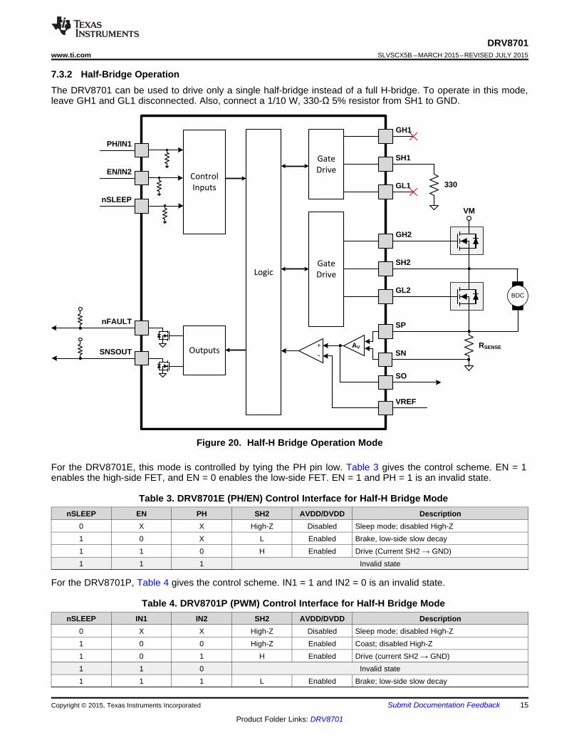
7.3.2 Half-Bridge OperationThe DRV8701 can be used to drive only a single half-bridge instead of a full H-bridge. To operate in this mode,leave GH1 and GL1 disconnected. Also, connect a 1/10 W, 330-Ω 5% resistor from SH1 to GND.
Figure 20. Half-H Bridge Operation Mode
For the DRV8701E, this mode is controlled by tying the PH pin low. Table 3 gives the control scheme. EN = 1enables the high-side FET, and EN = 0 enables the low-side FET. EN = 1 and PH = 1 is an invalid state.
Table 3. DRV8701E (PH/EN) Control Interface for Half-H Bridge ModenSLEEP EN PH SH2 AVDD/DVDD Description
0 X X High-Z Disabled Sleep mode; disabled High-Z1 0 X L Enabled Brake, low-side slow decay1 1 0 H Enabled Drive (Current SH2 → GND)1 1 1 Invalid state
For the DRV8701P, Table 4 gives the control scheme. IN1 = 1 and IN2 = 0 is an invalid state.
Table 4. DRV8701P (PWM) Control Interface for Half-H Bridge ModenSLEEP IN1 IN2 SH2 AVDD/DVDD Description
0 X X High-Z Disabled Sleep mode; disabled High-Z1 0 0 High-Z Enabled Coast; disabled High-Z1 0 1 H Enabled Drive (current SH2 → GND)1 1 0 Invalid state1 1 1 L Enabled Brake; low-side slow decay
Copyright © 2015, Texas Instruments Incorporated Submit Documentation Feedback 15
Product Folder Links: DRV8701
WWBLANK
Driv
e C
urre
nt (
A)
ICHOP
tOFF WWBLANK tOFF
SO
(V
)
VREF
SN
SO
UT
Drive Brake / Slow Decay Drive Brake / Slow Decay
REF OFFCHOP
V SENSE
9 ± 9I
A R
u
DRV8701SLVSCX5B –MARCH 2015–REVISED JULY 2015 www.ti.com
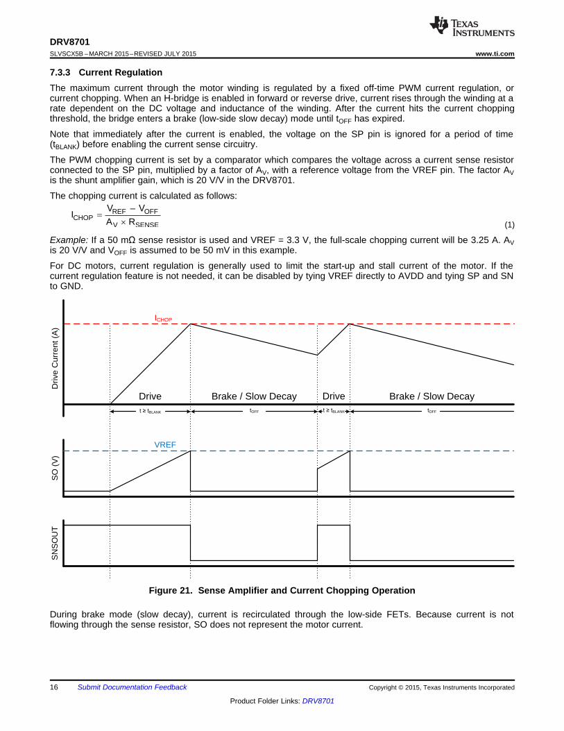
7.3.3 Current RegulationThe maximum current through the motor winding is regulated by a fixed off-time PWM current regulation, orcurrent chopping. When an H-bridge is enabled in forward or reverse drive, current rises through the winding at arate dependent on the DC voltage and inductance of the winding. After the current hits the current choppingthreshold, the bridge enters a brake (low-side slow decay) mode until tOFF has expired.
Note that immediately after the current is enabled, the voltage on the SP pin is ignored for a period of time(tBLANK) before enabling the current sense circuitry.
The PWM chopping current is set by a comparator which compares the voltage across a current sense resistorconnected to the SP pin, multiplied by a factor of AV, with a reference voltage from the VREF pin. The factor AVis the shunt amplifier gain, which is 20 V/V in the DRV8701.
The chopping current is calculated as follows:
(1)
Example: If a 50 mΩ sense resistor is used and VREF = 3.3 V, the full-scale chopping current will be 3.25 A. AVis 20 V/V and VOFF is assumed to be 50 mV in this example.
For DC motors, current regulation is generally used to limit the start-up and stall current of the motor. If thecurrent regulation feature is not needed, it can be disabled by tying VREF directly to AVDD and tying SP and SNto GND.
Figure 21. Sense Amplifier and Current Chopping Operation
During brake mode (slow decay), current is recirculated through the low-side FETs. Because current is notflowing through the sense resistor, SO does not represent the motor current.
16 Submit Documentation Feedback Copyright © 2015, Texas Instruments Incorporated
Product Folder Links: DRV8701

VOFF
Slope = AvSO
(V
)
SP - SN (V)
AVDD
SP
RSENSE
Logic
SNSOUT
VCC +
-
SOVREF
I
+
-
AV/(AV-1) x R
AV x R
R
SN
OFF
V SENSE
62 ± 9I
A R
u
DRV8701www.ti.com SLVSCX5B –MARCH 2015–REVISED JULY 2015
7.3.4 Amplifier Output SOThe SO pin on the DRV8701 outputs an analog voltage equal to the voltage seen across the SP and SN pinsmultiplied by AV. The factor AV is the shunt amplifier gain, which is 20 V/V in the DRV8701. SO is only validduring forward or reverse drive. The H-bridge current is approximately equal to:
(2)
When SP and SN are 0 V, SO outputs the amplifier offset voltage VOFF. No capacitor is required on the SO pin.
Figure 22. Sense Amplifier Diagram
If the voltage across SP and SN exceeds 1 V, then the DRV8701 flags an overcurrent condition.
The SO pin can source up to 5 mA of current. If the pin is shorted to GND, or if a higher-current load is driven bythis pin, the output acts as a constant-current source. The output voltage is not representative of the H-bridgecurrent in this state.
This shunt amplifier feature can be disabled by tying the SP and SN pins to GND. When the amplifier is disabled,current regulation is also disabled.
Figure 23. Sense Amplifier Output
7.3.4.1 SNSOUTThe SNSOUT pin of the DRV8701 indicates when the device is in current chopping mode. When the driver is ina slow decay mode caused by internal PWM current chopping (ICHOP threshold hit), the open-drain SNSOUToutput is pulled low. If the current regulation is disabled, then the SNSOUT pin will be high-Z.
Note that if the H-bridge is put into a slow decay mode using the inputs (PH/EN or IN1/IN2), then SNSOUT is notpulled low.
During forward or reverse drive mode, SNSOUT is high until the DRV8701 is internally forced into currentchopping. If the drive current rises above ICHOP, the driver enters a brake mode (low-side slow decay). TheSNSOUT pin will be pulled low during this current chopping brake mode. After the driver is re-enabled, theSNSOUT pin is released high-Z and the drive mode is restarted.Copyright © 2015, Texas Instruments Incorporated Submit Documentation Feedback 17
Product Folder Links: DRV8701

GH1
GL1
SH1
VGHS
VGLSPre-Drive
GH2
GL2
SH2
VGHS
VGLS
VM BDCLogic
PH or IN1
EN or IN2
SP
RSENSE
SN
nSLEEP
VM
Pre-Drive
ROFF
ROFF
ROFF
ROFF
DRV8701SLVSCX5B –MARCH 2015–REVISED JULY 2015 www.ti.com
7.3.5 PWM Motor Gate DriversThe DRV8701 contains gate drivers for a single H-bridge with external NMOS FETs. Figure 24 shows a blockdiagram of the gate driver circuitry.
Figure 24. PWM Motor Gate Drivers
Gate drivers inside the DRV8701 directly drive N-channel MOSFETs, which drive the motor current. The high-side gate drive is supplied by the charge pump, while the low-side gate drive voltage is generated by an internalregulator.
The peak drive current of the gate drivers is adjustable through the IDRIVE pin. Peak source currents may be setto 6, 12.5, 25, 100, or 150 mA. The peak sink current is approximately 2× the peak source current. Adjusting thepeak current changes the output slew rate, which also depends on the FET input capacitance and gate charge.
The peak drive current is selected by setting the value of the RIDRIVE resistor on the IDRIVE pin or by forcing avoltage onto the IDRIVE pin (see Table 6 for details).
Fast switching times can cause extra voltage noise on VM and GND. This can be especially due to a relativelyslow reverse-recovery time of the low-side body diode, where it conducts reverse-bias momentarily, being similarto shoot-through. Slow switching times can cause excessive power dissipation since the external FETs take alonger time to turn on and turn off.
18 Submit Documentation Feedback Copyright © 2015, Texas Instruments Incorporated
Product Folder Links: DRV8701

VG
S (
ga
te-t
o-s
ou
rce
) (V
)
QG gate charge (nC)
QGS QGD
VD
S (
dra
in-t
o-s
ou
rce
) (V
)
10
8
6
4
2
25
5040302010
20
15
10
5
Remaining QG
VGHS
VM
GHx
SHx
Pre-Drive
CGS
CGDG
S
D
High-side VGS
Low-side VGS
High-side gate drive
current
Low-side gate drive
current
tDRIVE
tDRIVE
IDR
IVE
,SR
C
IDR
IVE
,SR
C
IDR
IVE
,SN
K
IDR
IVE
,SN
K
IST
RO
NG
IST
RO
NG
IHOLD
IHOLD
IHOLD
IHOLD
IHOLD
IHOLD
DRV8701www.ti.com SLVSCX5B –MARCH 2015–REVISED JULY 2015
When changing the state of the output, the peak current (IDRIVE) is applied for a short drive period (tDRIVE) tocharge the gate capacitance. After this time, a weaker current source (IHOLD) is used to keep the gate at thedesired state. When selecting the gate drive strength for a given external FET, the selected current must be highenough to fully charge and discharge the gate during tDRIVE, or excessive power will be dissipated in the FET.
During high-side turn-on, the low-side gate is pulled low with a strong pull-down (ISTRONG). This prevents the low-side FET QGS from charging and keeps the FET off, even when there is fast switching at the outputs.
The pre-driver circuits include enforcement of a dead time in analog circuitry, which prevents the high-side andlow-side FETs from conducting at the same time. When switching FETs on, this handshaking prevents the high-or low-side FET from turning on until the opposite FET has been turned off.
Figure 25. Gate Driver Output to Control External FETs
QGD Miller chargeWhen a FET gate is turned on, three different capacitances must be charged.• QGS – Gate-to-source charge• QGD – Gate-to-drain charge (miller charge)• Remaining QG
The FET output is slewing primarily during the QGD charge.
Figure 26. Example FET Gate Charging Profile
Copyright © 2015, Texas Instruments Incorporated Submit Documentation Feedback 19
Product Folder Links: DRV8701
IDRIVE
«««
IDRIVE
RIDRIVE
IDRIVE
«««
IDRIVE
AVDD
RIDRIVE
IDRIVE
AVDD
«««
IDRIVE+
-2.5V
+
-1.3V
+
-0.1V
+
-3.7V
+
-4.3V
AVDD
190k
310k
Digital
Core
DRV8701SLVSCX5B –MARCH 2015–REVISED JULY 2015 www.ti.com
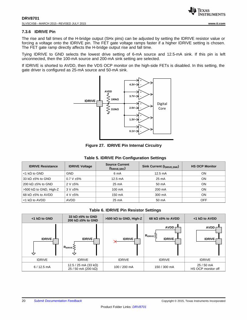
7.3.6 IDRIVE PinThe rise and fall times of the H-bridge output (SHx pins) can be adjusted by setting the IDRIVE resistor value orforcing a voltage onto the IDRIVE pin. The FET gate voltage ramps faster if a higher IDRIVE setting is chosen.The FET gate ramp directly affects the H-bridge output rise and fall time.
Tying IDRIVE to GND selects the lowest drive setting of 6-mA source and 12.5-mA sink. If this pin is leftunconnected, then the 100-mA source and 200-mA sink setting are selected.
If IDRIVE is shorted to AVDD, then the VDS OCP monitor on the high-side FETs is disabled. In this setting, thegate driver is configured as 25-mA source and 50-mA sink.
Figure 27. IDRIVE Pin Internal Circuitry
Table 5. IDRIVE Pin Configuration SettingsSource CurrentIDRIVE Resistance IDRIVE Voltage Sink Current (IDRIVE,SNK) HS OCP Monitor(IDRIVE,SRC)
<1 kΩ to GND GND 6 mA 12.5 mA ON33 kΩ ±5% to GND 0.7 V ±5% 12.5 mA 25 mA ON200 kΩ ±5% to GND 2 V ±5% 25 mA 50 mA ON>500 kΩ to GND, High-Z 3 V ±5% 100 mA 200 mA ON68 kΩ ±5% to AVDD 4 V ±5% 150 mA 300 mA ON<1 kΩ to AVDD AVDD 25 mA 50 mA OFF
Table 6. IDRIVE Pin Resistor Settings33 kΩ ±5% to GND<1 kΩ to GND >500 kΩ to GND, High-Z 68 kΩ ±5% to AVDD <1 kΩ to AVDD200 kΩ ±5% to GND
IDRIVE IDRIVE IDRIVE IDRIVE IDRIVE12.5 / 25 mA (33 kΩ) 25 / 50 mA6 / 12.5 mA 100 / 200 mA 150 / 300 mA25 / 50 mA (200 kΩ) HS OCP monitor off
20 Submit Documentation Feedback Copyright © 2015, Texas Instruments Incorporated
Product Folder Links: DRV8701

GH1
GL1
SH1
GH2
GL2
SH2
VM
BDC
High-side
VDS OCP
Monitor
High-side
VDS OCP
Monitor
Low-side
VDS OCP
Monitor
+
-
+
-
+
-
Low-side
VDS OCP
Monitor
+
-
VM
VM
SP
RSENSE
SN
DRV8701www.ti.com SLVSCX5B –MARCH 2015–REVISED JULY 2015
7.3.7 Dead TimeDead time (tDEAD) is measured as the time when SHx is High-Z between turning off one of the H-bridge FETsand turning on the other. For example, the output is High-Z between turning off the high-side FET and turning onthe low-side FET.
The DRV8701 inserts a digital dead time of approximately 150 ns. The total dead time also includes the FETgate turn-on time.
The total dead time is dependent on the IDRIVE resistor setting because a portion of the FET gate ramp (GHxand GLx pins) includes the observable dead time.
7.3.8 Propagation DelayThe propagation delay time (tDELAY) is measured as the time between an input edge to an output change. Thistime is composed of two parts: an input deglitch time and output slewing delay. The input deglitcher preventsnoise on the input pins from affecting the output state.
The gate drive slew rate also contributes to the delay time. For the output to change state during normaloperation, first, one FET must be turned off. The FET gate is ramped down according to the IDRIVE setting, andthe observed propagation delay ends when the FET gate has fallen below the threshold voltage.
7.3.9 Overcurrent VDS MonitorThe gate driver circuit monitors the VDS voltage of each external FET when it is driving current. When the voltagemonitored is greater than the OCP threshold voltage (VDS OCP), after the OCP deglitch time (tOCP) has expired, anOCP condition will be detected.
Figure 28. Overcurrent VDS Monitors
When IDRIVE is shorted to AVDD, the VDS OCP monitor on the high-side FETs is disabled. In cases where theVM supplied to the DRV8701 can be different from the external H-bridge supply, this setting must be used inorder to prevent false overcurrent detection. In this mode, the IDRIVE current is set to 25-mA source and 50-mAsink.
Copyright © 2015, Texas Instruments Incorporated Submit Documentation Feedback 21
Product Folder Links: DRV8701
AVDD
1 µF
VM
30 mAmax
4.8 V+
-
DVDD
1 µF
VM
30 mAmax
3.3 V+
-
VM
VCP
CPH
CPL
VMCharge
Pump
1 µF
0.1 µF
DRV8701SLVSCX5B –MARCH 2015–REVISED JULY 2015 www.ti.com
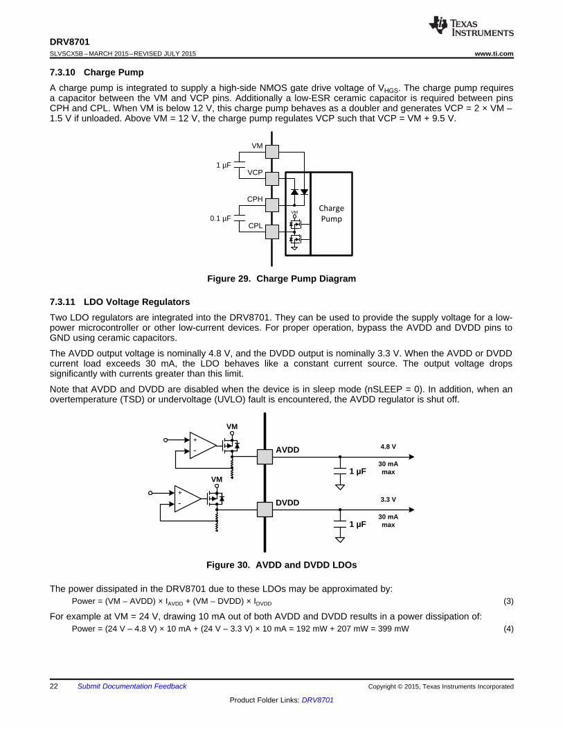
7.3.10 Charge PumpA charge pump is integrated to supply a high-side NMOS gate drive voltage of VHGS. The charge pump requiresa capacitor between the VM and VCP pins. Additionally a low-ESR ceramic capacitor is required between pinsCPH and CPL. When VM is below 12 V, this charge pump behaves as a doubler and generates VCP = 2 × VM –1.5 V if unloaded. Above VM = 12 V, the charge pump regulates VCP such that VCP = VM + 9.5 V.
Figure 29. Charge Pump Diagram
7.3.11 LDO Voltage RegulatorsTwo LDO regulators are integrated into the DRV8701. They can be used to provide the supply voltage for a low-power microcontroller or other low-current devices. For proper operation, bypass the AVDD and DVDD pins toGND using ceramic capacitors.
The AVDD output voltage is nominally 4.8 V, and the DVDD output is nominally 3.3 V. When the AVDD or DVDDcurrent load exceeds 30 mA, the LDO behaves like a constant current source. The output voltage dropssignificantly with currents greater than this limit.
Note that AVDD and DVDD are disabled when the device is in sleep mode (nSLEEP = 0). In addition, when anovertemperature (TSD) or undervoltage (UVLO) fault is encountered, the AVDD regulator is shut off.
Figure 30. AVDD and DVDD LDOs
The power dissipated in the DRV8701 due to these LDOs may be approximated by:Power = (VM – AVDD) × IAVDD + (VM – DVDD) × IDVDD (3)
For example at VM = 24 V, drawing 10 mA out of both AVDD and DVDD results in a power dissipation of:Power = (24 V – 4.8 V) × 10 mA + (24 V – 3.3 V) × 10 mA = 192 mW + 207 mW = 399 mW (4)
22 Submit Documentation Feedback Copyright © 2015, Texas Instruments Incorporated
Product Folder Links: DRV8701

GHx
SHx
IREVERSE
VGS > VCLAMP
ICLAMP
VMVGHS
Pre-Drive
GLx
VGLS
RSENSE
GND
VGS negative
DRV8701www.ti.com SLVSCX5B –MARCH 2015–REVISED JULY 2015
7.3.12 Gate Drive ClampA clamping structure limits the gate drive output voltage to VGS CLAMP to protect the power FETs from damage.The positive voltage clamp is realized using a series of diodes. The negative voltage clamp uses the body diodesof the internal gate driver FET.
Figure 31. Gate Drive Clamp Diagram
Copyright © 2015, Texas Instruments Incorporated Submit Documentation Feedback 23
Product Folder Links: DRV8701

DRV8701SLVSCX5B –MARCH 2015–REVISED JULY 2015 www.ti.com
7.3.13 Protection CircuitsThe DRV8701 is fully protected against VM undervoltage, charge pump undervoltage, overcurrent, gate drivershorts, and overtemperature events.
7.3.13.1 VM Undervoltage Lockout (UVLO)If at any time the voltage on the VM pin falls below the UVLO threshold voltage, all FETs in the H-bridge aredisabled, the charge pump is disabled, AVDD is disabled, and the nFAULT pin is driven low. Operation resumeswhen VM rises above the UVLO threshold. The nFAULT pin is released after operation has resumed.
7.3.13.2 VCP Undervoltage Lockout (CPUV)If at any time the voltage on the VCP pin falls below the charge pump undervoltage threshold voltage (VCPUV), allFETs in the H-bridge are disabled and the nFAULT pin is driven low. Operation resumes when VCP rises abovethe CPUV threshold. The nFAULT pin is released after operation has resumed.
7.3.13.3 Overcurrent Protection (OCP)Overcurrent is sensed by monitoring the VDS voltage drop across the external FETs (see Figure 28). If thevoltage across a driven FET exceeds the overcurrent trip threshold (VDS OCP) for longer than the OCP deglitchtime (tOCP), an OCP event is recognized. As a result, all FETs in the H-bridge are disabled and the nFAULT pin isdriven low; the driver is re-enabled after the OCP retry period (tRETRY) has passed. nFAULT releases high-Zagain at after the retry time. If the fault condition is still present, the cycle repeats. If the fault is no longer present,normal operation resumes and nFAULT remains released high-Z.
This VDS overcurrent monitor on the high-side FETs can be disabled by using a specific IDRIVE setting. Thisallows the system to have a higher DRV8701 VM supply than the H-bridge supply.
In addition to this FET VDS monitor, an overcurrent condition is also detected if the voltage at SP exceedsVSP OCP.
7.3.13.4 Pre-Driver Fault (PDF)The GHx and GLx pins are monitored such that if the voltage on the external FET gate does not increase above1 V (when sourcing current) or decrease below 1 V (when sinking current) after tDRIVE, a pre-driver fault isdetected. The device encounters this fault if GHx or GLx are shorted to GND, SHx, or VM. Additionally, thedevice encounters the pre-driver fault if the IDRIVE setting selected is not sufficient to turn on the external FET.As a result, all FETs in the H-bridge are disabled and the nFAULT pin is driven low. The driver is re-enabled afterthe retry period (tRETRY) has passed. The nFAULT pin is released after operation has resumed.
7.3.13.5 Thermal Shutdown (TSD)If the die temperature exceeds TTSD, all FETs in the H-bridge are disabled, the charge pump is shut down, AVDDis disabled, and the nFAULT pin is driven low. After the die temperature has fallen below TTSD – THYS, operationautomatically resumes. The nFAULT pin is released after operation has resumed.
Table 7. Fault ResponseFault Condition H-Bridge Charge Pump AVDD DVDD Recovery
VM undervoltage VM ≤ VUVLO Disabled Disabled Disabled Operating VM ≥ VUVLO(UVLO)VCP undervoltage VCP < VCPUV Disabled Operating Operating Operating VCP > VCPUV(CPUV)External FET overload VDS ≥ 1.0 V or Disabled Operating Operating Operating tRETRY(OCP) VSP – VSN > 1.0 V
Gate voltagePre-driver fault (PDF) Disabled Operating Operating Operating tRETRYunchanged after tDRIVE
Thermal shutdown TJ ≥ 150°C Disabled Disabled Disabled Operating TJ ≤ 130°C(TSD)
24 Submit Documentation Feedback Copyright © 2015, Texas Instruments Incorporated
Product Folder Links: DRV8701
GH1
GL1
SH1
GH2
GL2
SH2
BDC
SP
RSENSE
SN
VM
VM
1 µF0.1 µF
VCPCP2CP1
10 k 43 k
0.1 µFBulk
10 µF min
+
DRV8701www.ti.com SLVSCX5B –MARCH 2015–REVISED JULY 2015
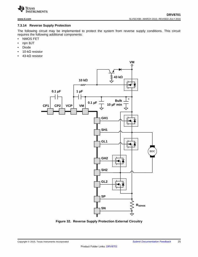
7.3.14 Reverse Supply ProtectionThe following circuit may be implemented to protect the system from reverse supply conditions. This circuitrequires the following additional components:• NMOS FET• npn BJT• Diode• 10-kΩ resistor• 43-kΩ resistor
Figure 32. Reverse Supply Protection External Circuitry
Copyright © 2015, Texas Instruments Incorporated Submit Documentation Feedback 25
Product Folder Links: DRV8701
DRV8701SLVSCX5B –MARCH 2015–REVISED JULY 2015 www.ti.com
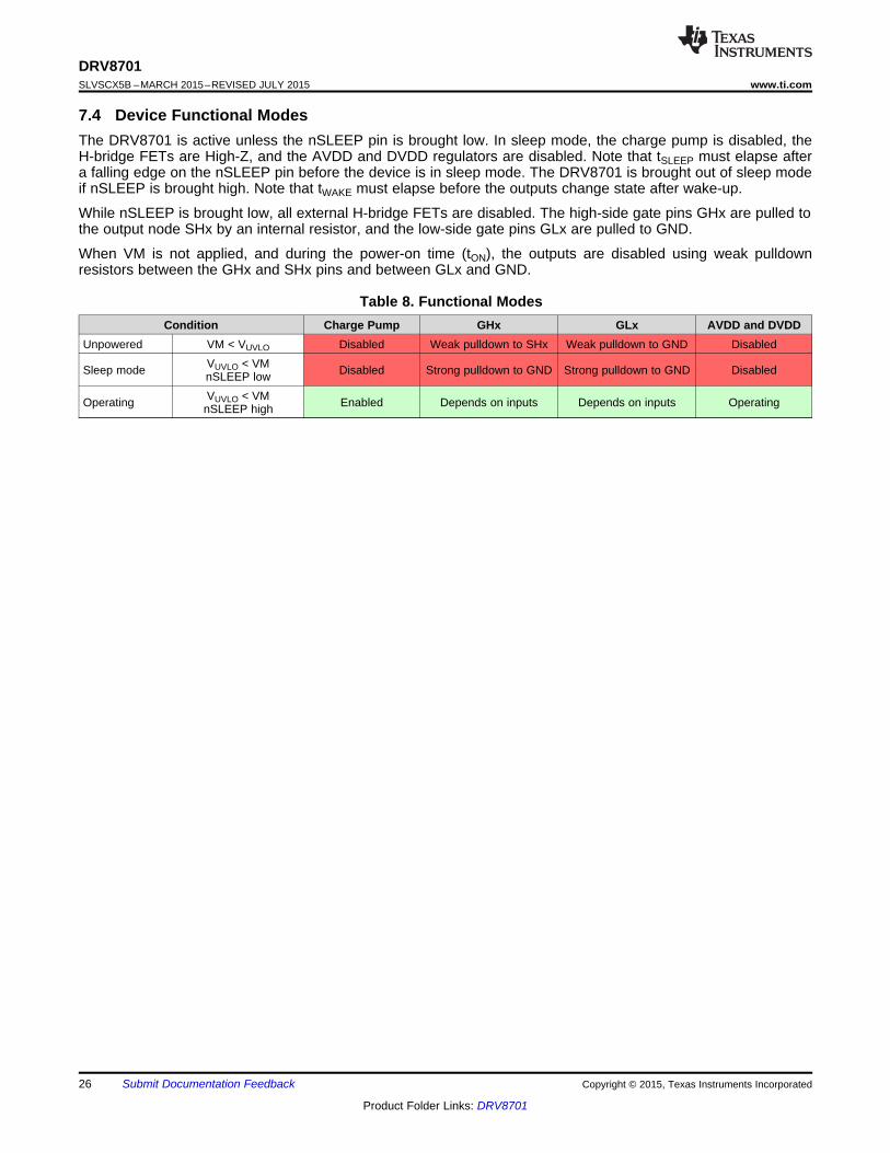
7.4 Device Functional ModesThe DRV8701 is active unless the nSLEEP pin is brought low. In sleep mode, the charge pump is disabled, theH-bridge FETs are High-Z, and the AVDD and DVDD regulators are disabled. Note that tSLEEP must elapse aftera falling edge on the nSLEEP pin before the device is in sleep mode. The DRV8701 is brought out of sleep modeif nSLEEP is brought high. Note that tWAKE must elapse before the outputs change state after wake-up.
While nSLEEP is brought low, all external H-bridge FETs are disabled. The high-side gate pins GHx are pulled tothe output node SHx by an internal resistor, and the low-side gate pins GLx are pulled to GND.
When VM is not applied, and during the power-on time (tON), the outputs are disabled using weak pulldownresistors between the GHx and SHx pins and between GLx and GND.
Table 8. Functional ModesCondition Charge Pump GHx GLx AVDD and DVDD
Unpowered VM < VUVLO Disabled Weak pulldown to SHx Weak pulldown to GND DisabledVUVLO < VMSleep mode Disabled Strong pulldown to GND Strong pulldown to GND DisablednSLEEP lowVUVLO < VMOperating Enabled Depends on inputs Depends on inputs OperatingnSLEEP high
26 Submit Documentation Feedback Copyright © 2015, Texas Instruments Incorporated
Product Folder Links: DRV8701

DRV8701www.ti.com SLVSCX5B –MARCH 2015–REVISED JULY 2015
7.4.1 Operating DRV8701 and H-Bridge on Separate SuppliesThe DRV8701 can operate with a different supply voltage (VM) than the system H-bridge supply (VBAT). Case 1describes normal operation when VM and VBAT are roughly the same. Special considerations must be taken intoaccount for Cases 2, 3, and 4.• Case 1: VM ≈ VBAT. Recommended operation• Case 2: VM > VBAT. IDRIVE must be shorted to AVDD to disable the high-side OCP. The IDRIVE current is
fixed at 25-mA source and 50-mA sink. This case can allow the driver to better enhance the external FETs forVBAT < 11.5 V, or operate down to a lower supply voltage below 5.9 V.
• Case 3: VM > VBAT (higher than Case 2). IDRIVE must be shorted to AVDD to disable the high-side OCP.This case can also allow the driver to better enhance the external FETs, or operate down to a lower supplyvoltage below 5.9 V. The IDRIVE current is fixed at 25-mA source and 50-mA sink. Excess gate drive currentmay be driven through the DRV8701 gate clamps causing additional power dissipation in the DRV8701.
• Case 4: VM < VBAT. The high-side FETs may not be in saturation. There may be a significant voltage dropacross the high-side FET when driving current. This causes high power dissipation in the external FET. Whenoperating in Case 4, the external FET threshold voltage must be greater than 2 V. Otherwise the DRV8701will report a pre-driver fault whenever the FET is out of saturation.
Table 9. VM Operational Range based on VBATVBAT Range Case 3 Case 2 Case 1 Case 4
VM ≥ 5.9 V1 V ≤ VBAT < 5.9 V N/A N/AVM < 0.5 × VBAT + 5.75 VVM ≥ 0.5 × VBAT + 5.75 V VM ≥ 5.9 V5.9 V ≤ VBAT < 6.4 V VM ≤ 45 V VM = VBATVM > VBAT VM < VBAT
VM < 0.5 × VBAT + 5.75 V6.4 V ≤ VBAT < 11.5 V VM > 0.6 × VBAT + 2.5 V VM ≥ 5.9 V
VM ≤ VBAT VM ≤ 0.6 × VBAT + 2.5 V11.5 V ≤ VBAT < 14 VVM > VBAT N/A VM > VBAT – 4 V VM ≥ 5.9 VVM ≤ 45 V14 V ≤ VBAT ≤ 45 V VM ≤ VBAT VM ≤ VBAT – 4 V
Figure 33. VM Operating Range Based on Motor Supply Voltage
When nSLEEP is low, VM may be reduced down to 0 V with up to 45 V present at VBAT. However, nSLEEPshould not be brought high until VM is supplied with a voltage aligning with one of the cases outlined above.
Copyright © 2015, Texas Instruments Incorporated Submit Documentation Feedback 27
Product Folder Links: DRV8701
VM
VCP
CPH
CPL
GND
VREF
GH2
SH2
GL2
SP
SN
GL1
SH1
GH1
GND
PH
EN
nSLEEP
AVDD
DVDD
nFAULT
SNSOUT
SO
IDRIVE
123456
18
17
16
15
14
13
24
23
22
21
20
19
7
8
9
10
11
12
GND
(PPAD)
0.1 µF Bulk+
VM1 µF0.1 µFR1 R2
33 k
10 k 10 k 1 µF
1 µF
50 m
VM
VM
BDC
DRV8701SLVSCX5B –MARCH 2015–REVISED JULY 2015 www.ti.com
8 Application and Implementation
NOTEInformation in the following applications sections is not part of the TI componentspecification, and TI does not warrant its accuracy or completeness. TI’s customers areresponsible for determining suitability of components for their purposes. Customers shouldvalidate and test their design implementation to confirm system functionality.
8.1 Application InformationThe DRV8701 is used in brushed-DC, solenoid, or relay control.
8.2 Typical Applications
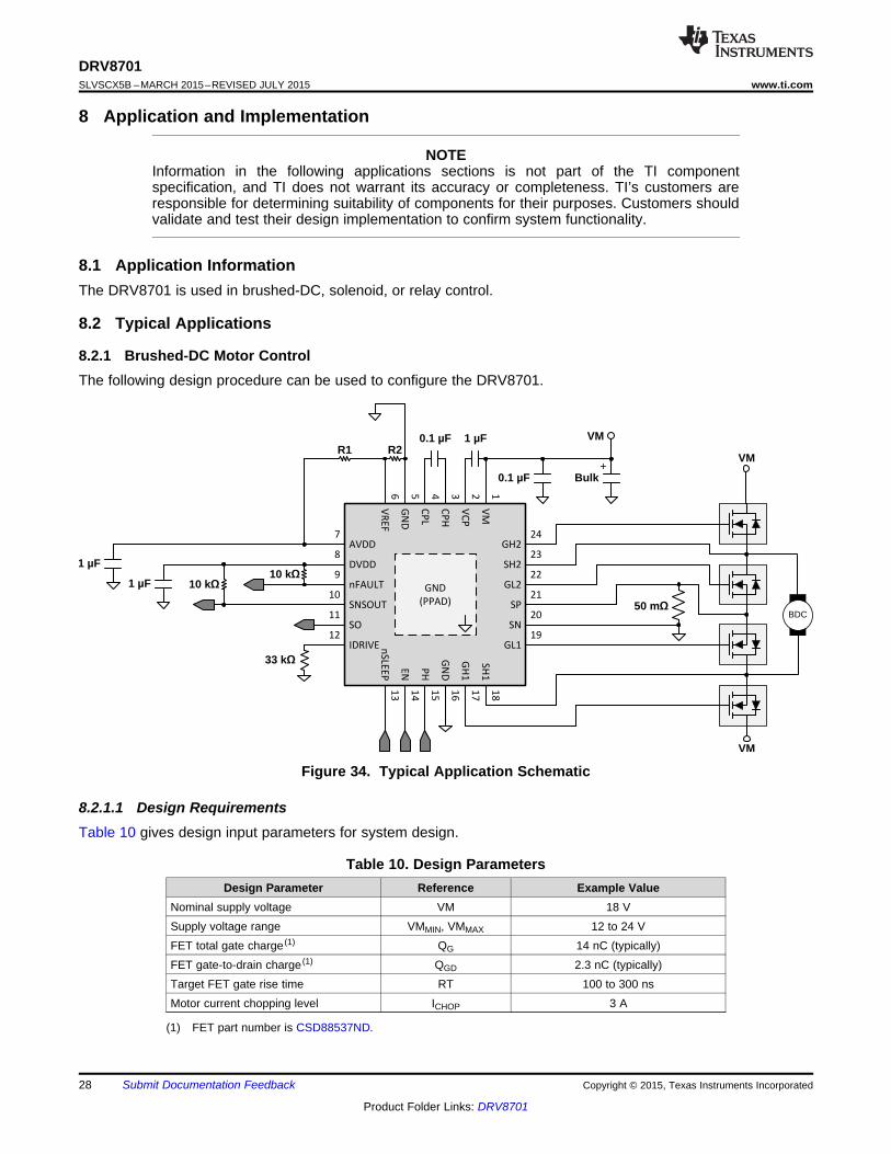
8.2.1 Brushed-DC Motor ControlThe following design procedure can be used to configure the DRV8701.
Figure 34. Typical Application Schematic
8.2.1.1 Design RequirementsTable 10 gives design input parameters for system design.
Table 10. Design ParametersDesign Parameter Reference Example Value
Nominal supply voltage VM 18 VSupply voltage range VMMIN, VMMAX 12 to 24 VFET total gate charge (1) QG 14 nC (typically)FET gate-to-drain charge (1) QGD 2.3 nC (typically)Target FET gate rise time RT 100 to 300 nsMotor current chopping level ICHOP 3 A
(1) FET part number is CSD88537ND.
28 Submit Documentation Feedback Copyright © 2015, Texas Instruments Incorporated
Product Folder Links: DRV8701

O FFCHO P
V SENSE
95() ± 9I
A R
u
GDQIDRIVE
RT!
VCPG
PWM
IQ
¦
u
PWMOFF BLANK
1¦ N+]
t t |
VCPG
PWM
IQ
¦
DRV8701www.ti.com SLVSCX5B –MARCH 2015–REVISED JULY 2015
8.2.1.2 Detailed Design Procedure
8.2.1.2.1 External FET Selection
The DRV8701 FET support is based on the charge pump capacity and output PWM frequency. For a quickcalculation of FET driving capacity, use the following equations when drive and brake (slow decay) are theprimary modes of operation:
where• fPWM is the maximum desired PWM frequency to be applied to the DRV8701 inputs or the current chopping
frequency, whichever is larger.• IVCP is the charge pump capacity, which depends on VM. (5)
The internal current chopping frequency is at most:
(6)
Example: If a system at VM = 7 V (IVCP = 8 mA) uses a maximum PWM frequency of 40 kHz, then the DRV8701will support QG < 200 nC FETs.
If the application will require a forced fast decay (or alternating between drive and reverse drive), the maximumFET driving capacity is given by:
(7)
8.2.1.2.2 IDRIVE Configuration
Select IDRIVE based on the gate charge of the FETs. Configure this pin so that the FET gates are chargedcompletely during tDRIVE. If the designer chooses an IDRIVE that is too low for a given FET, then the FET maynot turn on completely. TI suggests to adjust these values in-system with the required external FETs and motorto determine the best possible setting for any application.
For FETs with a known gate-to-drain charge (QGD) and desired rise time (RT), select IDRIVE based on:
(8)
Example: If the gate-to-drain charge is 2.3 nC, and the desired rise time is around 100 to 300 ns,IDRIVE1 = 2.3 nC / 100 ns = 23 mAIDRIVE2 = 2.3 nC / 300 ns = 7.7 mASelect IDRIVE between 7.7 and 23 mASelect IDRIVE as 12.5-mA source (25-mA sink)Requires a 33-kΩ resistor from the IDRIVE pin to GND
8.2.1.2.3 Current Chopping Configuration
The chopping current is set based on the sense resistor value and the analog voltage at VREF. Calculate thecurrent using Equation 9. The amplifier gain AV is 20 V/V and VOFF is typically 50 mV.
Example: If the desired chopping current is 3 A,Set RSENSE = 50 mΩ
(9)
VREF would have to be 3.05 V.Create a resistor divider from AVDD (4.8 V) to set VREF ≈ 3 VSet R2 = 3.3 kΩ; set R1 = 2 kΩ.
Copyright © 2015, Texas Instruments Incorporated Submit Documentation Feedback 29
Product Folder Links: DRV8701

DRV8701SLVSCX5B –MARCH 2015–REVISED JULY 2015 www.ti.com
8.2.1.3 Application Curves
Figure 35. SH1 Rise Time (12.5-mA Source, 25-mA Sink) Figure 36. SH1 Fall Time (12.5-mA Source, 25-mA Sink)
Figure 37. Current Regulating at 3 A on Motor Startup Figure 38. Current Profile on Motor Startup WithRegulation
Figure 39. Current Profile on Motor Startup Without Regulation
30 Submit Documentation Feedback Copyright © 2015, Texas Instruments Incorporated
Product Folder Links: DRV8701

VM
VCP
CPH
CPL
GND
VREF
GH2
SH2
GL2
SP
SN
GL1
SH1
GH1
GND
PH
EN
nSLEEP
AVDD
DVDD
nFAULT
SNSOUT
SO
IDRIVE
123456
18
17
16
15
14
13
24
23
22
21
20
19
7
8
9
10
11
12
0.01 µF
1 µF0.1 µFR1 R2
68 k
10 k 10 k 1 µF
1 µF
50 m
VBAT
VBAT
BDC
Boost
0.1 µF10 µF+
AVDD
C1+
GND
(PPAD)
DRV8701www.ti.com SLVSCX5B –MARCH 2015–REVISED JULY 2015
8.2.2 Alternate ApplicationIn this example, the DRV8701 is powered from a supply that is boosted above VBAT. This allows the system towork at lower VBAT voltages, but requires the user to disable OCP monitoring.
Figure 40. DRV8701 on Boosted Supply
8.2.2.1 Design RequirementsTable 11 gives design input parameters for system design.
Table 11. Design ParametersDesign Parameter Reference Example Value
12 V nominalBattery voltage VBAT Minimum operation: 4.0 VVM = 7 V when VBAT < 7 VDRV8701 supply voltage VM VM = VBAT when VBAT ≥ 7 V
FET total gate charge QG 42 nCFET gate-to-drain charge QGD 11 nCMotor current chopping level ICHOP 3 A
8.2.3 Detailed Design Procedure
8.2.3.1 IDRIVE ConfigurationBecause the VM supply to the DRV8701 is different from the external H-bridge supply VBAT, the designer mustdisable the overcurrent monitor to prevent false overcurrent detection. The designer must place a 68-kΩ resistorbetween the IDRIVE pin and AVDD.
IDRIVE is fixed at 25-mA source and 50-mA sink in this mode.
So, the rise time is 11 nC / 25 mA = 440 ns.
Copyright © 2015, Texas Instruments Incorporated Submit Documentation Feedback 31
Product Folder Links: DRV8701
Local Bulk Capacitor
Parasitic WireInductance
+±
Motor Driver
Power Supply Motor Drive System
VM
GND
+
IC Bypass Capacitor
VBAT + 11.5 VVM <
2
DRV8701SLVSCX5B –MARCH 2015–REVISED JULY 2015 www.ti.com
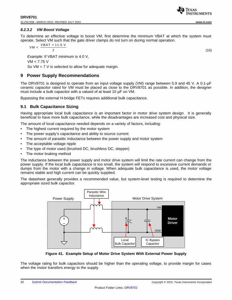
8.2.3.2 VM Boost VoltageTo determine an effective voltage to boost VM, first determine the minimum VBAT at which the system mustoperate. Select VM such that the gate driver clamps do not turn on during normal operation.
(10)
Example: If VBAT minimum is 4.0 V,VM < 7.75 VSo VM = 7 V is selected to allow for adequate margin.
9 Power Supply RecommendationsThe DRV8701 is designed to operate from an input voltage supply (VM) range between 5.9 and 45 V. A 0.1-µFceramic capacitor rated for VM must be placed as close to the DRV8701 as possible. In addition, the designermust include a bulk capacitor with a valued of at least 10 µF on VM.
Bypassing the external H-bridge FETs requires additional bulk capacitance.
9.1 Bulk Capacitance SizingHaving appropriate local bulk capacitance is an important factor in motor drive system design. It is generallybeneficial to have more bulk capacitance, while the disadvantages are increased cost and physical size.
The amount of local capacitance needed depends on a variety of factors, including:• The highest current required by the motor system• The power supply’s capacitance and ability to source current• The amount of parasitic inductance between the power supply and motor system• The acceptable voltage ripple• The type of motor used (brushed DC, brushless DC, stepper)• The motor braking method
The inductance between the power supply and motor drive system will limit the rate current can change from thepower supply. If the local bulk capacitance is too small, the system will respond to excessive current demands ordumps from the motor with a change in voltage. When adequate bulk capacitance is used, the motor voltageremains stable and high current can be quickly supplied.
The datasheet generally provides a recommended value, but system-level testing is required to determine theappropriate sized bulk capacitor.
Figure 41. Example Setup of Motor Drive System With External Power Supply
The voltage rating for bulk capacitors should be higher than the operating voltage, to provide margin for caseswhen the motor transfers energy to the supply.
32 Submit Documentation Feedback Copyright © 2015, Texas Instruments Incorporated
Product Folder Links: DRV8701
1 µF0.1 µF
123456
18
17
16
15
14
13
24
23
22
21
20
7
8
9
10
11
12
VM
VCP
CPH
CPL
GND
VREF
SH1
GH1
GND
PH
EN
nSLEEP
AVDD
DVDD
nFAULT
SNSOUT
SO
IDRIVE GL1
SN
SP
GL2
SH2
GH2
GND(PPAD)
19
RIDRIVE
1 µF
1 µF
0.1 µF
D
D
D
D
G
S
S
S
S
D
D
D
D
G
S
S
S
S
S
G
D
D
D
D
S
S
S
G
D
D
D
D
RSENSE
VM
VM
GN
D
SH
1S
H2
10 µF minimum
GND
GND
GND+
DRV8701www.ti.com SLVSCX5B –MARCH 2015–REVISED JULY 2015
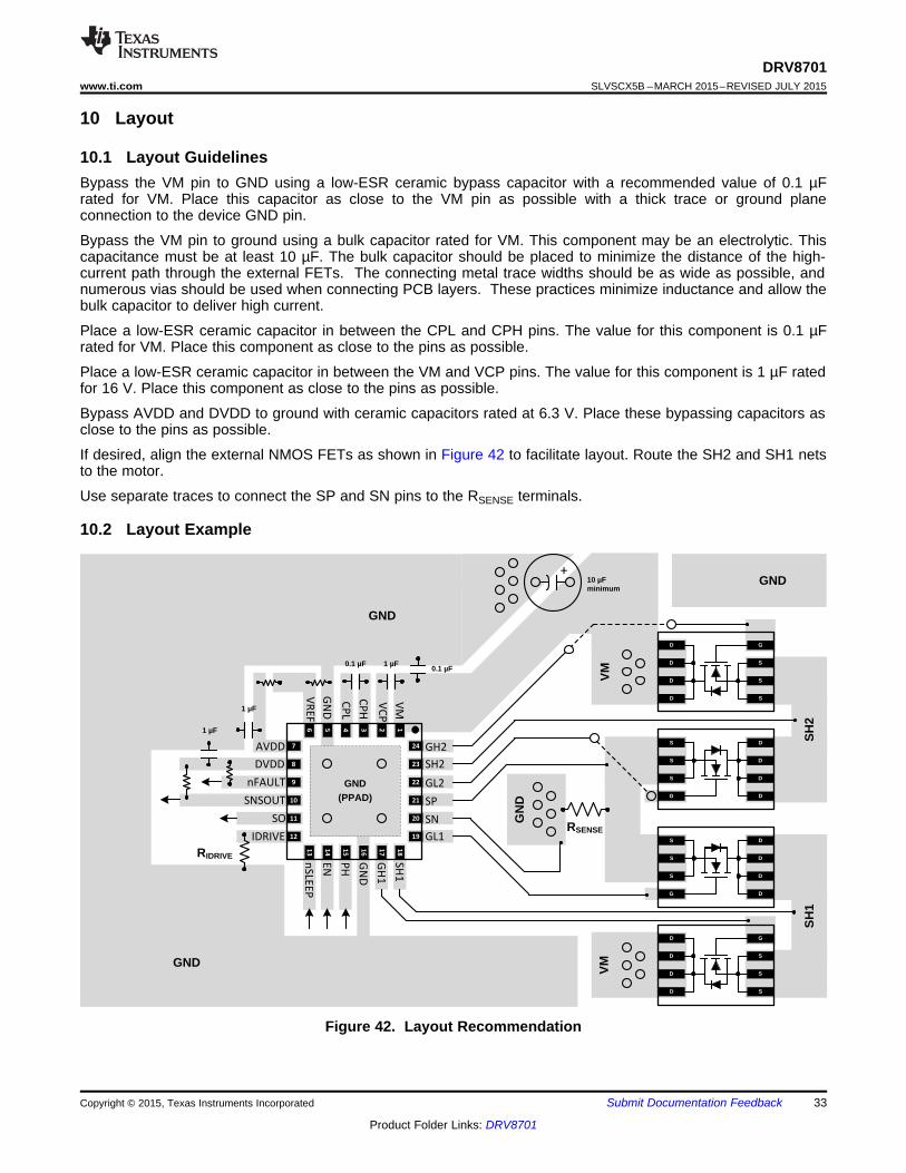
10 Layout
10.1 Layout GuidelinesBypass the VM pin to GND using a low-ESR ceramic bypass capacitor with a recommended value of 0.1 µFrated for VM. Place this capacitor as close to the VM pin as possible with a thick trace or ground planeconnection to the device GND pin.
Bypass the VM pin to ground using a bulk capacitor rated for VM. This component may be an electrolytic. Thiscapacitance must be at least 10 µF. The bulk capacitor should be placed to minimize the distance of the high-current path through the external FETs. The connecting metal trace widths should be as wide as possible, andnumerous vias should be used when connecting PCB layers. These practices minimize inductance and allow thebulk capacitor to deliver high current.
Place a low-ESR ceramic capacitor in between the CPL and CPH pins. The value for this component is 0.1 µFrated for VM. Place this component as close to the pins as possible.
Place a low-ESR ceramic capacitor in between the VM and VCP pins. The value for this component is 1 µF ratedfor 16 V. Place this component as close to the pins as possible.
Bypass AVDD and DVDD to ground with ceramic capacitors rated at 6.3 V. Place these bypassing capacitors asclose to the pins as possible.
If desired, align the external NMOS FETs as shown in Figure 42 to facilitate layout. Route the SH2 and SH1 netsto the motor.
Use separate traces to connect the SP and SN pins to the RSENSE terminals.
10.2 Layout Example
Figure 42. Layout Recommendation
Copyright © 2015, Texas Instruments Incorporated Submit Documentation Feedback 33
Product Folder Links: DRV8701
DRV8701SLVSCX5B –MARCH 2015–REVISED JULY 2015 www.ti.com
11 Device and Documentation Support
11.1 Documentation Support
11.1.1 Related Documentation• PowerPAD™ Thermally Enhanced Package, SLMA002• PowerPAD™ Made Easy, SLMA004• Current Recirculation and Decay Modes, SLVA321
11.2 Community ResourcesThe following links connect to TI community resources. Linked contents are provided "AS IS" by the respectivecontributors. They do not constitute TI specifications and do not necessarily reflect TI's views; see TI's Terms ofUse.
TI E2E™ Online Community TI's Engineer-to-Engineer (E2E) Community. Created to foster collaborationamong engineers. At e2e.ti.com, you can ask questions, share knowledge, explore ideas and helpsolve problems with fellow engineers.
Design Support TI's Design Support Quickly find helpful E2E forums along with design support tools andcontact information for technical support.
11.3 TrademarksPowerPAD, E2E are trademarks of Texas Instruments.All other trademarks are the property of their respective owners.
11.4 Electrostatic Discharge CautionThese devices have limited built-in ESD protection. The leads should be shorted together or the device placed in conductive foamduring storage or handling to prevent electrostatic damage to the MOS gates.
11.5 GlossarySLYZ022 — TI Glossary.
This glossary lists and explains terms, acronyms, and definitions.
12 Mechanical, Packaging, and Orderable InformationThe following pages include mechanical, packaging, and orderable information. This information is the mostcurrent data available for the designated devices. This data is subject to change without notice and revision ofthis document. For browser-based versions of this data sheet, refer to the left-hand navigation.
34 Submit Documentation Feedback Copyright © 2015, Texas Instruments Incorporated
Product Folder Links: DRV8701
PACKAGE OPTION ADDENDUM
www.ti.com 30-Jun-2015
Addendum-Page 1
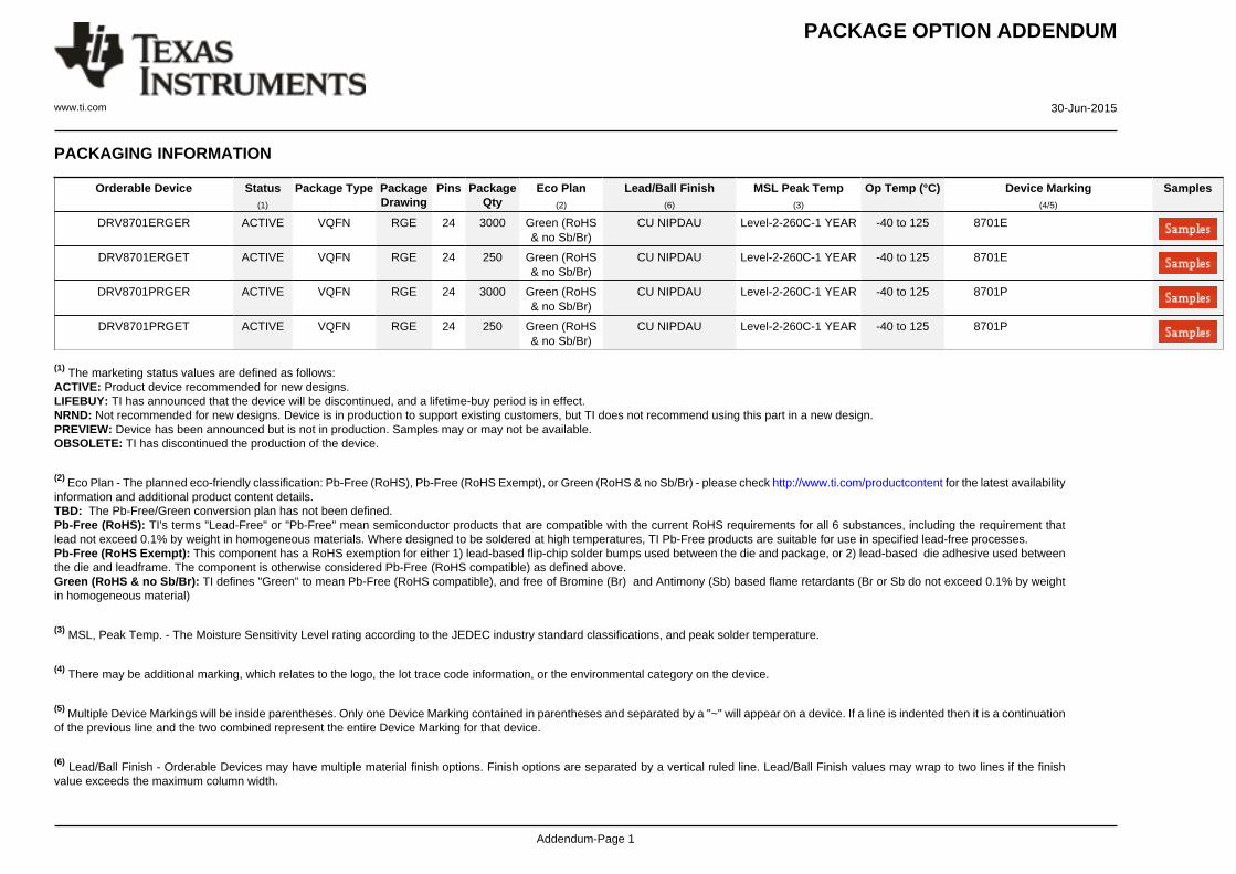
PACKAGING INFORMATION
Orderable Device Status(1)
Package Type PackageDrawing
Pins PackageQty
Eco Plan(2)
Lead/Ball Finish(6)
MSL Peak Temp(3)
Op Temp (°C) Device Marking(4/5)
Samples
DRV8701ERGER ACTIVE VQFN RGE 24 3000 Green (RoHS& no Sb/Br)
CU NIPDAU Level-2-260C-1 YEAR -40 to 125 8701E
DRV8701ERGET ACTIVE VQFN RGE 24 250 Green (RoHS& no Sb/Br)
CU NIPDAU Level-2-260C-1 YEAR -40 to 125 8701E
DRV8701PRGER ACTIVE VQFN RGE 24 3000 Green (RoHS& no Sb/Br)
CU NIPDAU Level-2-260C-1 YEAR -40 to 125 8701P
DRV8701PRGET ACTIVE VQFN RGE 24 250 Green (RoHS& no Sb/Br)
CU NIPDAU Level-2-260C-1 YEAR -40 to 125 8701P
(1) The marketing status values are defined as follows:ACTIVE: Product device recommended for new designs.LIFEBUY: TI has announced that the device will be discontinued, and a lifetime-buy period is in effect.NRND: Not recommended for new designs. Device is in production to support existing customers, but TI does not recommend using this part in a new design.PREVIEW: Device has been announced but is not in production. Samples may or may not be available.OBSOLETE: TI has discontinued the production of the device.
(2) Eco Plan - The planned eco-friendly classification: Pb-Free (RoHS), Pb-Free (RoHS Exempt), or Green (RoHS & no Sb/Br) - please check http://www.ti.com/productcontent for the latest availabilityinformation and additional product content details.TBD: The Pb-Free/Green conversion plan has not been defined.Pb-Free (RoHS): TI's terms "Lead-Free" or "Pb-Free" mean semiconductor products that are compatible with the current RoHS requirements for all 6 substances, including the requirement thatlead not exceed 0.1% by weight in homogeneous materials. Where designed to be soldered at high temperatures, TI Pb-Free products are suitable for use in specified lead-free processes.Pb-Free (RoHS Exempt): This component has a RoHS exemption for either 1) lead-based flip-chip solder bumps used between the die and package, or 2) lead-based die adhesive used betweenthe die and leadframe. The component is otherwise considered Pb-Free (RoHS compatible) as defined above.Green (RoHS & no Sb/Br): TI defines "Green" to mean Pb-Free (RoHS compatible), and free of Bromine (Br) and Antimony (Sb) based flame retardants (Br or Sb do not exceed 0.1% by weightin homogeneous material)
(3) MSL, Peak Temp. - The Moisture Sensitivity Level rating according to the JEDEC industry standard classifications, and peak solder temperature.
(4) There may be additional marking, which relates to the logo, the lot trace code information, or the environmental category on the device.
(5) Multiple Device Markings will be inside parentheses. Only one Device Marking contained in parentheses and separated by a "~" will appear on a device. If a line is indented then it is a continuationof the previous line and the two combined represent the entire Device Marking for that device.
(6) Lead/Ball Finish - Orderable Devices may have multiple material finish options. Finish options are separated by a vertical ruled line. Lead/Ball Finish values may wrap to two lines if the finishvalue exceeds the maximum column width.
PACKAGE OPTION ADDENDUM
www.ti.com 30-Jun-2015
Addendum-Page 2
Important Information and Disclaimer:The information provided on this page represents TI's knowledge and belief as of the date that it is provided. TI bases its knowledge and belief on informationprovided by third parties, and makes no representation or warranty as to the accuracy of such information. Efforts are underway to better integrate information from third parties. TI has taken andcontinues to take reasonable steps to provide representative and accurate information but may not have conducted destructive testing or chemical analysis on incoming materials and chemicals.TI and TI suppliers consider certain information to be proprietary, and thus CAS numbers and other limited information may not be available for release.
In no event shall TI's liability arising out of such information exceed the total purchase price of the TI part(s) at issue in this document sold by TI to Customer on an annual basis.

TAPE AND REEL INFORMATION
*All dimensions are nominal
Device PackageType
PackageDrawing
Pins SPQ ReelDiameter
(mm)
ReelWidth
W1 (mm)
A0(mm)
B0(mm)
K0(mm)
P1(mm)
W(mm)
Pin1Quadrant
DRV8701ERGER VQFN RGE 24 3000 330.0 12.4 4.25 4.25 1.15 8.0 12.0 Q2
DRV8701ERGET VQFN RGE 24 250 180.0 12.4 4.25 4.25 1.15 8.0 12.0 Q2
DRV8701PRGER VQFN RGE 24 3000 330.0 12.4 4.25 4.25 1.15 8.0 12.0 Q2
DRV8701PRGET VQFN RGE 24 250 180.0 12.4 4.25 4.25 1.15 8.0 12.0 Q2
PACKAGE MATERIALS INFORMATION
www.ti.com 30-Jun-2015
Pack Materials-Page 1

*All dimensions are nominal
Device Package Type Package Drawing Pins SPQ Length (mm) Width (mm) Height (mm)
DRV8701ERGER VQFN RGE 24 3000 367.0 367.0 35.0
DRV8701ERGET VQFN RGE 24 250 210.0 185.0 35.0
DRV8701PRGER VQFN RGE 24 3000 367.0 367.0 35.0
DRV8701PRGET VQFN RGE 24 250 210.0 185.0 35.0
PACKAGE MATERIALS INFORMATION
www.ti.com 30-Jun-2015
Pack Materials-Page 2

GENERIC PACKAGE VIEW
Images above are just a representation of the package family, actual package may vary.Refer to the product data sheet for package details.
RGE 24 VQFN - 1 mm max heightPLASTIC QUAD FLATPACK - NO LEAD
4204104/H

www.ti.com
PACKAGE OUTLINE
C
SEE TERMINALDETAIL 24X 0.30
0.18
2.8 0.1
24X 0.50.3
1 MAX
(0.2) TYP
0.050.00
20X 0.5
2X2.5
2X 2.5
A 4.13.9
B
4.13.9
0.300.18
0.50.3
4222437/A 12/2015
VQFN - 1 mm max heightRGE0024FPLASTIC QUAD FLATPACK - NO LEAD
PIN 1 INDEX AREA
0.08
SEATING PLANE
1
6 13
18
7 12
24 19(OPTIONAL)
PIN 1 ID 0.1 C A B0.05
EXPOSEDTHERMAL PAD
25
NOTES: 1. All linear dimensions are in millimeters. Any dimensions in parenthesis are for reference only. Dimensioning and tolerancing per ASME Y14.5M. 2. This drawing is subject to change without notice. 3. The package thermal pad must be soldered to the printed circuit board for thermal and mechanical performance.4. Reference JEDEC registration MO-220.
SCALE 3.300
DETAILOPTIONAL TERMINAL
TYPICAL

www.ti.com
EXAMPLE BOARD LAYOUT
0.05 MINALL AROUND
0.05 MAXALL AROUND
24X (0.24)
24X (0.6)
( ) TYPVIA
0.2
20X (0.5)(3.8)
(3.8)
(1.15)TYP
( 2.8)
(R )ALL PAD CORNERS
0.05
4222437/A 12/2015
VQFN - 1 mm max heightRGE0024FPLASTIC QUAD FLATPACK - NO LEAD
SYMM
1
6
7 12
13
18
1924
SYMM
LAND PATTERN EXAMPLESCALE:18X
25
NOTES: (continued) 5. This package is designed to be soldered to a thermal pad on the board. For more information, see Texas Instruments literature number SLUA271 (www.ti.com/lit/slua271).6. Vias are optional depending on application, refer to device data sheet. If some or all are implemented, recommended via locations are shown.
SOLDER MASKOPENING
METAL UNDERSOLDER MASK
SOLDER MASKDEFINED
METAL
SOLDER MASKOPENING
SOLDER MASK DETAILS
NON SOLDER MASKDEFINED
(PREFERRED)
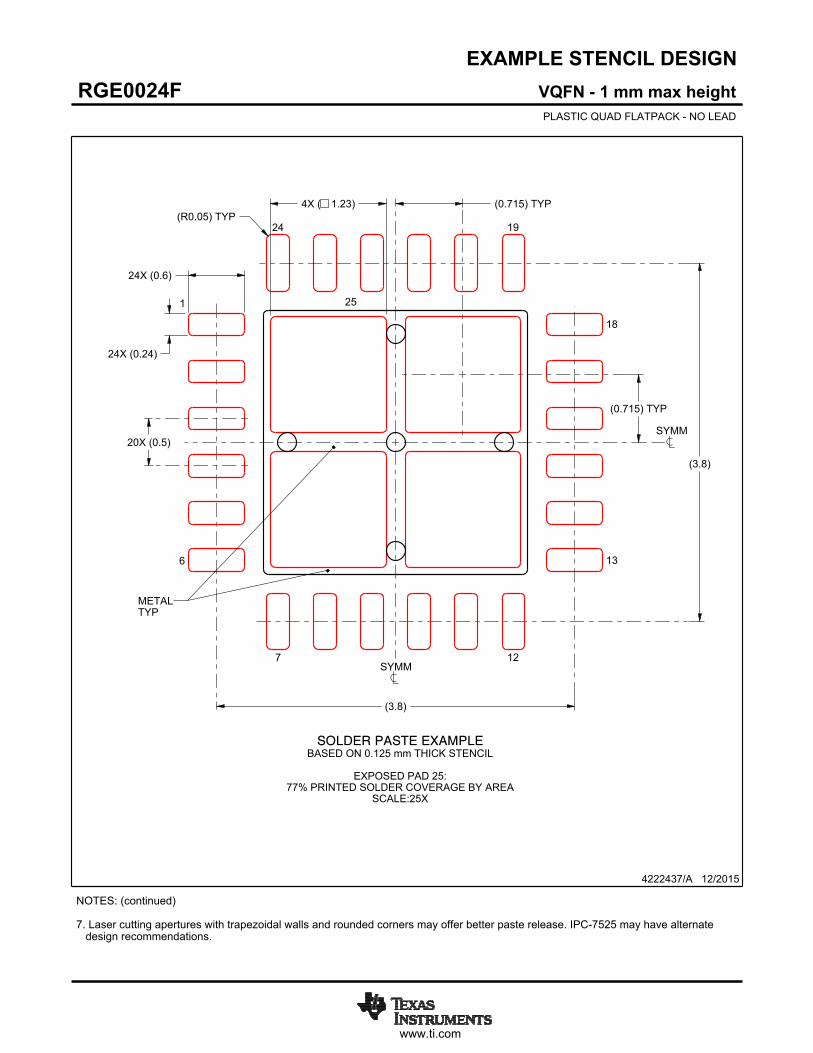
www.ti.com
EXAMPLE STENCIL DESIGN
24X (0.6)
24X (0.24)
20X (0.5)
(3.8)
(3.8)
4X ( 1.23)
(0.715) TYP
(0.715) TYP(R ) TYP0.05
4222437/A 12/2015
VQFN - 1 mm max heightRGE0024FPLASTIC QUAD FLATPACK - NO LEAD
NOTES: (continued) 7. Laser cutting apertures with trapezoidal walls and rounded corners may offer better paste release. IPC-7525 may have alternate design recommendations.
25
SYMM
METALTYP
SOLDER PASTE EXAMPLEBASED ON 0.125 mm THICK STENCIL
EXPOSED PAD 25:
77% PRINTED SOLDER COVERAGE BY AREASCALE:25X
SYMM
1
6
7 12
13
18
1924

IMPORTANT NOTICE
Texas Instruments Incorporated (TI) reserves the right to make corrections, enhancements, improvements and other changes to itssemiconductor products and services per JESD46, latest issue, and to discontinue any product or service per JESD48, latest issue. Buyersshould obtain the latest relevant information before placing orders and should verify that such information is current and complete.TI’s published terms of sale for semiconductor products (http://www.ti.com/sc/docs/stdterms.htm) apply to the sale of packaged integratedcircuit products that TI has qualified and released to market. Additional terms may apply to the use or sale of other types of TI products andservices.Reproduction of significant portions of TI information in TI data sheets is permissible only if reproduction is without alteration and isaccompanied by all associated warranties, conditions, limitations, and notices. TI is not responsible or liable for such reproduceddocumentation. Information of third parties may be subject to additional restrictions. Resale of TI products or services with statementsdifferent from or beyond the parameters stated by TI for that product or service voids all express and any implied warranties for theassociated TI product or service and is an unfair and deceptive business practice. TI is not responsible or liable for any such statements.Buyers and others who are developing systems that incorporate TI products (collectively, “Designers”) understand and agree that Designersremain responsible for using their independent analysis, evaluation and judgment in designing their applications and that Designers havefull and exclusive responsibility to assure the safety of Designers' applications and compliance of their applications (and of all TI productsused in or for Designers’ applications) with all applicable regulations, laws and other applicable requirements. Designer represents that, withrespect to their applications, Designer has all the necessary expertise to create and implement safeguards that (1) anticipate dangerousconsequences of failures, (2) monitor failures and their consequences, and (3) lessen the likelihood of failures that might cause harm andtake appropriate actions. Designer agrees that prior to using or distributing any applications that include TI products, Designer willthoroughly test such applications and the functionality of such TI products as used in such applications.TI’s provision of technical, application or other design advice, quality characterization, reliability data or other services or information,including, but not limited to, reference designs and materials relating to evaluation modules, (collectively, “TI Resources”) are intended toassist designers who are developing applications that incorporate TI products; by downloading, accessing or using TI Resources in anyway, Designer (individually or, if Designer is acting on behalf of a company, Designer’s company) agrees to use any particular TI Resourcesolely for this purpose and subject to the terms of this Notice.TI’s provision of TI Resources does not expand or otherwise alter TI’s applicable published warranties or warranty disclaimers for TIproducts, and no additional obligations or liabilities arise from TI providing such TI Resources. TI reserves the right to make corrections,enhancements, improvements and other changes to its TI Resources. TI has not conducted any testing other than that specificallydescribed in the published documentation for a particular TI Resource.Designer is authorized to use, copy and modify any individual TI Resource only in connection with the development of applications thatinclude the TI product(s) identified in such TI Resource. NO OTHER LICENSE, EXPRESS OR IMPLIED, BY ESTOPPEL OR OTHERWISETO ANY OTHER TI INTELLECTUAL PROPERTY RIGHT, AND NO LICENSE TO ANY TECHNOLOGY OR INTELLECTUAL PROPERTYRIGHT OF TI OR ANY THIRD PARTY IS GRANTED HEREIN, including but not limited to any patent right, copyright, mask work right, orother intellectual property right relating to any combination, machine, or process in which TI products or services are used. Informationregarding or referencing third-party products or services does not constitute a license to use such products or services, or a warranty orendorsement thereof. Use of TI Resources may require a license from a third party under the patents or other intellectual property of thethird party, or a license from TI under the patents or other intellectual property of TI.TI RESOURCES ARE PROVIDED “AS IS” AND WITH ALL FAULTS. TI DISCLAIMS ALL OTHER WARRANTIES ORREPRESENTATIONS, EXPRESS OR IMPLIED, REGARDING RESOURCES OR USE THEREOF, INCLUDING BUT NOT LIMITED TOACCURACY OR COMPLETENESS, TITLE, ANY EPIDEMIC FAILURE WARRANTY AND ANY IMPLIED WARRANTIES OFMERCHANTABILITY, FITNESS FOR A PARTICULAR PURPOSE, AND NON-INFRINGEMENT OF ANY THIRD PARTY INTELLECTUALPROPERTY RIGHTS. TI SHALL NOT BE LIABLE FOR AND SHALL NOT DEFEND OR INDEMNIFY DESIGNER AGAINST ANY CLAIM,INCLUDING BUT NOT LIMITED TO ANY INFRINGEMENT CLAIM THAT RELATES TO OR IS BASED ON ANY COMBINATION OFPRODUCTS EVEN IF DESCRIBED IN TI RESOURCES OR OTHERWISE. IN NO EVENT SHALL TI BE LIABLE FOR ANY ACTUAL,DIRECT, SPECIAL, COLLATERAL, INDIRECT, PUNITIVE, INCIDENTAL, CONSEQUENTIAL OR EXEMPLARY DAMAGES INCONNECTION WITH OR ARISING OUT OF TI RESOURCES OR USE THEREOF, AND REGARDLESS OF WHETHER TI HAS BEENADVISED OF THE POSSIBILITY OF SUCH DAMAGES.Unless TI has explicitly designated an individual product as meeting the requirements of a particular industry standard (e.g., ISO/TS 16949and ISO 26262), TI is not responsible for any failure to meet such industry standard requirements.Where TI specifically promotes products as facilitating functional safety or as compliant with industry functional safety standards, suchproducts are intended to help enable customers to design and create their own applications that meet applicable functional safety standardsand requirements. Using products in an application does not by itself establish any safety features in the application. Designers mustensure compliance with safety-related requirements and standards applicable to their applications. Designer may not use any TI products inlife-critical medical equipment unless authorized officers of the parties have executed a special contract specifically governing such use.Life-critical medical equipment is medical equipment where failure of such equipment would cause serious bodily injury or death (e.g., lifesupport, pacemakers, defibrillators, heart pumps, neurostimulators, and implantables). Such equipment includes, without limitation, allmedical devices identified by the U.S. Food and Drug Administration as Class III devices and equivalent classifications outside the U.S.TI may expressly designate certain products as completing a particular qualification (e.g., Q100, Military Grade, or Enhanced Product).Designers agree that it has the necessary expertise to select the product with the appropriate qualification designation for their applicationsand that proper product selection is at Designers’ own risk. Designers are solely responsible for compliance with all legal and regulatoryrequirements in connection with such selection.Designer will fully indemnify TI and its representatives against any damages, costs, losses, and/or liabilities arising out of Designer’s non-compliance with the terms and provisions of this Notice.
Mailing Address: Texas Instruments, Post Office Box 655303, Dallas, Texas 75265Copyright © 2018, Texas Instruments Incorporated