

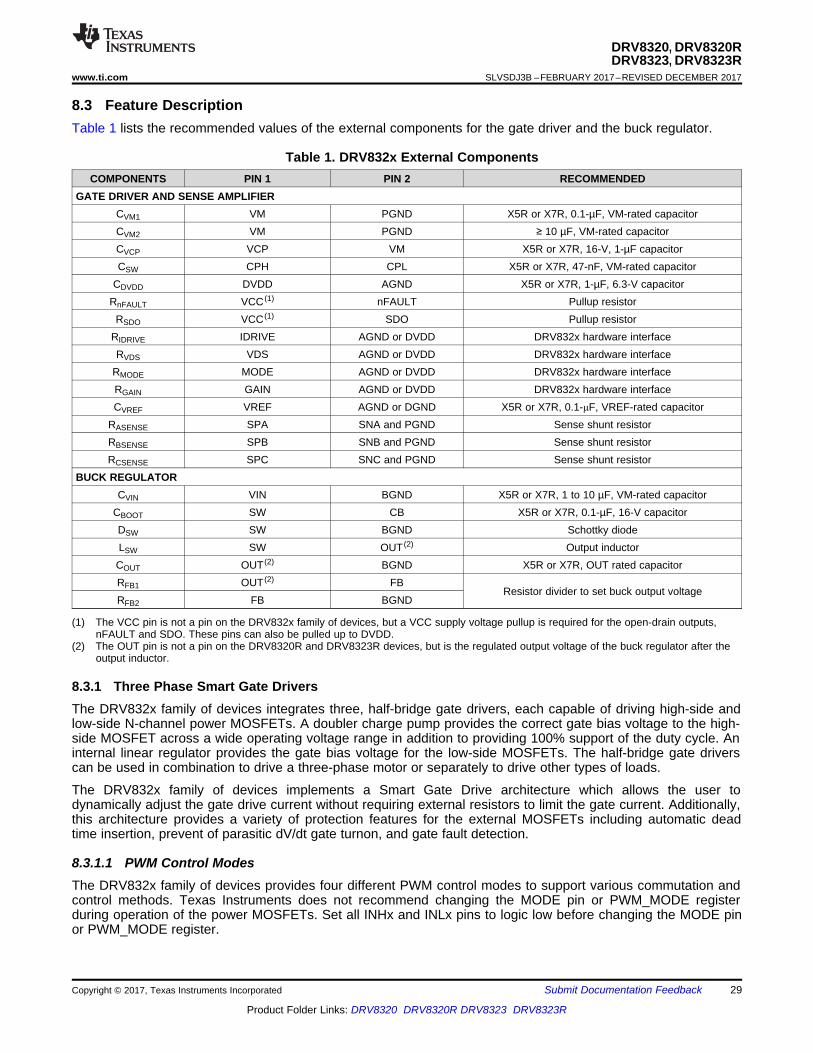
DRV832x 6 to 60-V Three-Phase Smart Gate Driver · PDF file6 to 60 V DRV832x Three-Phase Smart...
90
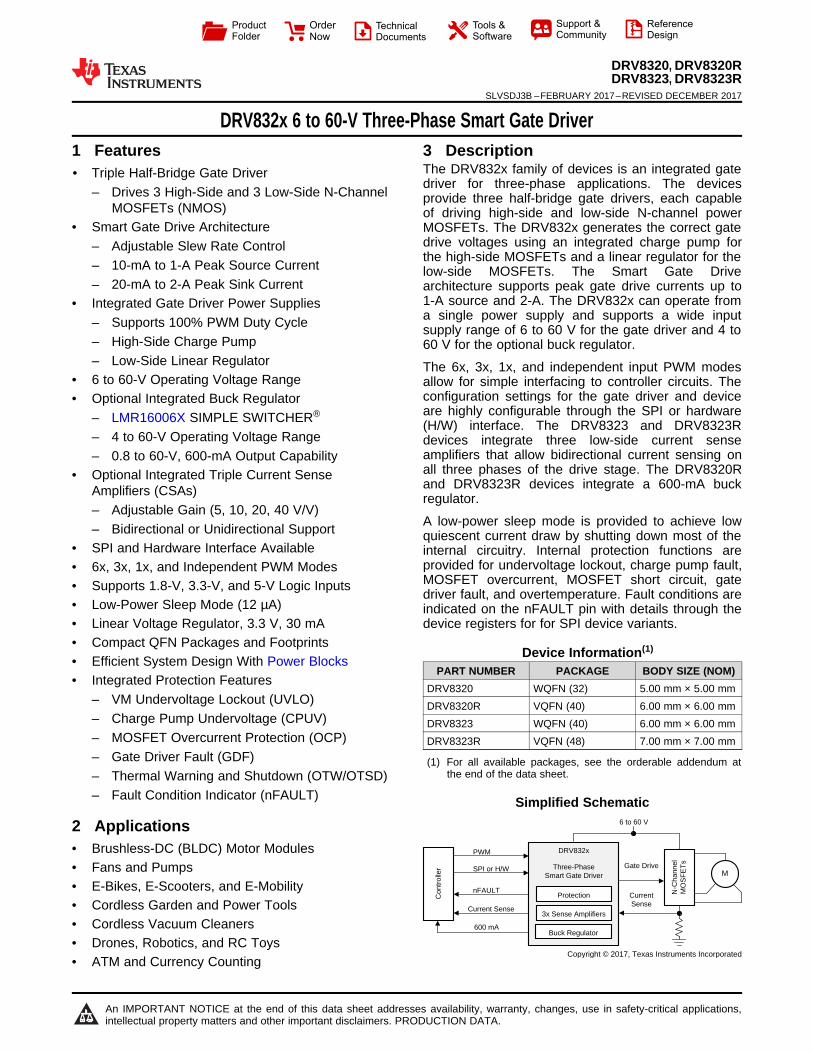
6 to 60 V DRV832x Three-Phase Smart Gate Driver PWM Gate Drive Current Sense Current Sense 3x Sense Amplifiers N-Channel MOSFETs nFAULT M SPI or H/W 600 mA Protection Controller Buck Regulator Copyright © 2017, Texas Instruments Incorporated Product Folder Order Now Technical Documents Tools & Software Support & Community Reference Design An IMPORTANT NOTICE at the end of this data sheet addresses availability, warranty, changes, use in safety-critical applications, intellectual property matters and other important disclaimers. PRODUCTION DATA. DRV8320, DRV8320R DRV8323, DRV8323R SLVSDJ3B – FEBRUARY 2017 – REVISED DECEMBER 2017 DRV832x 6 to 60-V Three-Phase Smart Gate Driver 1 1 Features 1• Triple Half-Bridge Gate Driver – Drives 3 High-Side and 3 Low-Side N-Channel MOSFETs (NMOS) • Smart Gate Drive Architecture – Adjustable Slew Rate Control – 10-mA to 1-A Peak Source Current – 20-mA to 2-A Peak Sink Current • Integrated Gate Driver Power Supplies – Supports 100% PWM Duty Cycle – High-Side Charge Pump – Low-Side Linear Regulator • 6 to 60-V Operating Voltage Range • Optional Integrated Buck Regulator – LMR16006X SIMPLE SWITCHER ® – 4 to 60-V Operating Voltage Range – 0.8 to 60-V, 600-mA Output Capability • Optional Integrated Triple Current Sense Amplifiers (CSAs) – Adjustable Gain (5, 10, 20, 40 V/V) – Bidirectional or Unidirectional Support • SPI and Hardware Interface Available • 6x, 3x, 1x, and Independent PWM Modes • Supports 1.8-V, 3.3-V, and 5-V Logic Inputs • Low-Power Sleep Mode (12 μA) • Linear Voltage Regulator, 3.3 V, 30 mA • Compact QFN Packages and Footprints • Efficient System Design With Power Blocks • Integrated Protection Features – VM Undervoltage Lockout (UVLO) – Charge Pump Undervoltage (CPUV) – MOSFET Overcurrent Protection (OCP) – Gate Driver Fault (GDF) – Thermal Warning and Shutdown (OTW/OTSD) – Fault Condition Indicator (nFAULT) 2 Applications • Brushless-DC (BLDC) Motor Modules • Fans and Pumps • E-Bikes, E-Scooters, and E-Mobility • Cordless Garden and Power Tools • Cordless Vacuum Cleaners • Drones, Robotics, and RC Toys • ATM and Currency Counting 3 Description The DRV832x family of devices is an integrated gate driver for three-phase applications. The devices provide three half-bridge gate drivers, each capable of driving high-side and low-side N-channel power MOSFETs. The DRV832x generates the correct gate drive voltages using an integrated charge pump for the high-side MOSFETs and a linear regulator for the low-side MOSFETs. The Smart Gate Drive architecture supports peak gate drive currents up to 1-A source and 2-A. The DRV832x can operate from a single power supply and supports a wide input supply range of 6 to 60 V for the gate driver and 4 to 60 V for the optional buck regulator. The 6x, 3x, 1x, and independent input PWM modes allow for simple interfacing to controller circuits. The configuration settings for the gate driver and device are highly configurable through the SPI or hardware (H/W) interface. The DRV8323 and DRV8323R devices integrate three low-side current sense amplifiers that allow bidirectional current sensing on all three phases of the drive stage. The DRV8320R and DRV8323R devices integrate a 600-mA buck regulator. A low-power sleep mode is provided to achieve low quiescent current draw by shutting down most of the internal circuitry. Internal protection functions are provided for undervoltage lockout, charge pump fault, MOSFET overcurrent, MOSFET short circuit, gate driver fault, and overtemperature. Fault conditions are indicated on the nFAULT pin with details through the device registers for for SPI device variants. Device Information (1) PART NUMBER PACKAGE BODY SIZE (NOM) DRV8320 WQFN (32) 5.00 mm × 5.00 mm DRV8320R VQFN (40) 6.00 mm × 6.00 mm DRV8323 WQFN (40) 6.00 mm × 6.00 mm DRV8323R VQFN (48) 7.00 mm × 7.00 mm (1) For all available packages, see the orderable addendum at the end of the data sheet. Simplified Schematic
Transcript of DRV832x 6 to 60-V Three-Phase Smart Gate Driver · PDF file6 to 60 V DRV832x Three-Phase Smart...
6 to 60 V
DRV832x
Three-Phase Smart Gate Driver
PWM
Gate Drive
Current Sense
Current Sense3x Sense Amplifiers
N-C
hann
el
MO
SF
ET
s
nFAULT
MSPI or H/W
600 mA
ProtectionCon
trol
ler
Buck Regulator
Copyright © 2017, Texas Instruments Incorporated
Product
Folder
Order
Now
Technical
Documents
Tools &
Software
Support &Community
ReferenceDesign
An IMPORTANT NOTICE at the end of this data sheet addresses availability, warranty, changes, use in safety-critical applications,intellectual property matters and other important disclaimers. PRODUCTION DATA.
DRV8320, DRV8320RDRV8323, DRV8323R
SLVSDJ3B –FEBRUARY 2017–REVISED DECEMBER 2017
DRV832x 6 to 60-V Three-Phase Smart Gate Driver
1
1 Features1• Triple Half-Bridge Gate Driver
– Drives 3 High-Side and 3 Low-Side N-ChannelMOSFETs (NMOS)
• Smart Gate Drive Architecture– Adjustable Slew Rate Control– 10-mA to 1-A Peak Source Current– 20-mA to 2-A Peak Sink Current
• Integrated Gate Driver Power Supplies– Supports 100% PWM Duty Cycle– High-Side Charge Pump– Low-Side Linear Regulator
• 6 to 60-V Operating Voltage Range• Optional Integrated Buck Regulator
– LMR16006X SIMPLE SWITCHER®
– 4 to 60-V Operating Voltage Range– 0.8 to 60-V, 600-mA Output Capability
• Optional Integrated Triple Current SenseAmplifiers (CSAs)– Adjustable Gain (5, 10, 20, 40 V/V)– Bidirectional or Unidirectional Support
• SPI and Hardware Interface Available• 6x, 3x, 1x, and Independent PWM Modes• Supports 1.8-V, 3.3-V, and 5-V Logic Inputs• Low-Power Sleep Mode (12 µA)• Linear Voltage Regulator, 3.3 V, 30 mA• Compact QFN Packages and Footprints• Efficient System Design With Power Blocks• Integrated Protection Features
– VM Undervoltage Lockout (UVLO)– Charge Pump Undervoltage (CPUV)– MOSFET Overcurrent Protection (OCP)– Gate Driver Fault (GDF)– Thermal Warning and Shutdown (OTW/OTSD)– Fault Condition Indicator (nFAULT)
2 Applications• Brushless-DC (BLDC) Motor Modules• Fans and Pumps• E-Bikes, E-Scooters, and E-Mobility• Cordless Garden and Power Tools• Cordless Vacuum Cleaners• Drones, Robotics, and RC Toys• ATM and Currency Counting
3 DescriptionThe DRV832x family of devices is an integrated gatedriver for three-phase applications. The devicesprovide three half-bridge gate drivers, each capableof driving high-side and low-side N-channel powerMOSFETs. The DRV832x generates the correct gatedrive voltages using an integrated charge pump forthe high-side MOSFETs and a linear regulator for thelow-side MOSFETs. The Smart Gate Drivearchitecture supports peak gate drive currents up to1-A source and 2-A. The DRV832x can operate froma single power supply and supports a wide inputsupply range of 6 to 60 V for the gate driver and 4 to60 V for the optional buck regulator.
The 6x, 3x, 1x, and independent input PWM modesallow for simple interfacing to controller circuits. Theconfiguration settings for the gate driver and deviceare highly configurable through the SPI or hardware(H/W) interface. The DRV8323 and DRV8323Rdevices integrate three low-side current senseamplifiers that allow bidirectional current sensing onall three phases of the drive stage. The DRV8320Rand DRV8323R devices integrate a 600-mA buckregulator.
A low-power sleep mode is provided to achieve lowquiescent current draw by shutting down most of theinternal circuitry. Internal protection functions areprovided for undervoltage lockout, charge pump fault,MOSFET overcurrent, MOSFET short circuit, gatedriver fault, and overtemperature. Fault conditions areindicated on the nFAULT pin with details through thedevice registers for for SPI device variants.
Device Information(1)
PART NUMBER PACKAGE BODY SIZE (NOM)DRV8320 WQFN (32) 5.00 mm × 5.00 mmDRV8320R VQFN (40) 6.00 mm × 6.00 mmDRV8323 WQFN (40) 6.00 mm × 6.00 mmDRV8323R VQFN (48) 7.00 mm × 7.00 mm
(1) For all available packages, see the orderable addendum atthe end of the data sheet.
Simplified Schematic
2
DRV8320, DRV8320RDRV8323, DRV8323RSLVSDJ3B –FEBRUARY 2017–REVISED DECEMBER 2017 www.ti.com
Product Folder Links: DRV8320 DRV8320R DRV8323 DRV8323R
Submit Documentation Feedback Copyright © 2017, Texas Instruments Incorporated
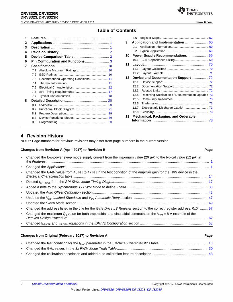
Table of Contents1 Features .................................................................. 12 Applications ........................................................... 13 Description ............................................................. 14 Revision History..................................................... 25 Device Comparison Table ..................................... 36 Pin Configuration and Functions ......................... 37 Specifications....................................................... 10
7.1 Absolute Maximum Ratings .................................... 107.2 ESD Ratings .......................................................... 107.3 Recommended Operating Conditions..................... 117.4 Thermal Information ................................................ 117.5 Electrical Characteristics......................................... 127.6 SPI Timing Requirements ....................................... 177.7 Typical Characteristics ............................................ 18
8 Detailed Description ............................................ 208.1 Overview ................................................................. 208.2 Functional Block Diagram ....................................... 218.3 Feature Description................................................. 298.4 Device Functional Modes........................................ 498.5 Programming........................................................... 50
8.6 Register Maps ......................................................... 529 Application and Implementation ........................ 60
9.1 Application Information............................................ 609.2 Typical Application ................................................. 60
10 Power Supply Recommendations ..................... 6910.1 Bulk Capacitance Sizing ....................................... 69
11 Layout................................................................... 7011.1 Layout Guidelines ................................................. 7011.2 Layout Example .................................................... 71
12 Device and Documentation Support ................. 7212.1 Device Support...................................................... 7212.2 Documentation Support ........................................ 7212.3 Related Links ........................................................ 7212.4 Receiving Notification of Documentation Updates 7312.5 Community Resources.......................................... 7312.6 Trademarks ........................................................... 7312.7 Electrostatic Discharge Caution............................ 7312.8 Glossary ................................................................ 73
13 Mechanical, Packaging, and OrderableInformation ........................................................... 73
4 Revision HistoryNOTE: Page numbers for previous revisions may differ from page numbers in the current version.
Changes from Revision A (April 2017) to Revision B Page
• Changed the low-power sleep mode supply current from the maximum value (20 µA) to the typical value (12 µA) inthe Features............................................................................................................................................................................ 1
• Changed the Applications....................................................................................................................................................... 1• Changed the GAIN value from 45 kΩ to 47 kΩ in the test condition of the amplifier gain for the H/W device in the
Electrical Characteristics table ............................................................................................................................................. 14• Deleted tEN_nSCS from the SPI Slave Mode Timing Diagram................................................................................................. 17• Added a note to the Synchronous 1x PWM Mode to define !PWM ..................................................................................... 30• Updated the Auto Offset Calibration section ........................................................................................................................ 43• Updated the VDS Latched Shutdown and VDS Automatic Retry sections ............................................................................. 47• Updated the Sleep Mode section ......................................................................................................................................... 49• Changed the address listed in the title for the Gate Drive LS Register section to the correct register address, 0x04 ........ 57• Changed the maximum Qg value for both trapezoidal and sinusoidal commutation the VVM = 8 V example of the
Detailed Design Procedure................................................................................................................................................... 62• Changed IDRIVEP and IDRIVEN equations in the IDRIVE Configuration section ....................................................................... 63
Changes from Original (February 2017) to Revision A Page
• Changed the test condition for the IBIAS parameter in the Electrical Characteristics table ................................................... 15• Changed the GHx values in the 3x PWM Mode Truth Table ............................................................................................... 30• Changed the calibration description and added auto calibration feature description .......................................................... 43
32C
PL
9S
LB1CPH 24 DVDD
31P
GN
D10
GLB
2VCP 23 AGND
30IN
LC11
SH
B3VM 22 ENABLE
29IN
HC
12G
HB
4VDRAIN 21 nSCS
28IN
LB13
GH
C5GHA 20 SCLK
27IN
HB
14S
HC
6SHA 19 SDI
26IN
LA15
GLC
7GLA 18 SDO
25IN
HA
16S
LC8SLA 17 nFAULT
Not to scale
Thermal
Pad
32C
PL
9S
LB
1CPH 24 DVDD
31P
GN
D10
GLB
2VCP 23 AGND
30IN
LC11
SH
B
3VM 22 ENABLE
29IN
HC
12G
HB
4VDRAIN 21 NC
28IN
LB13
GH
C
5GHA 20 VDS
27IN
HB
14S
HC
6SHA 19 IDRIVE
26IN
LA15
GLC
7GLA 18 MODE
25IN
HA
16S
LC
8SLA 17 nFAULT
Not to scale
Thermal
Pad
3
DRV8320, DRV8320RDRV8323, DRV8323R
www.ti.com SLVSDJ3B –FEBRUARY 2017–REVISED DECEMBER 2017
Product Folder Links: DRV8320 DRV8320R DRV8323 DRV8323R
Submit Documentation FeedbackCopyright © 2017, Texas Instruments Incorporated
(1) For more information on the device name and device options, see the Device Nomenclature section.
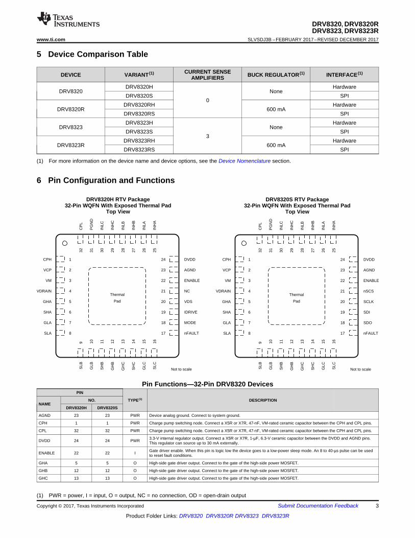
5 Device Comparison Table
DEVICE VARIANT (1) CURRENT SENSEAMPLIFIERS BUCK REGULATOR (1) INTERFACE (1)
DRV8320DRV8320H
0None
HardwareDRV8320S SPI
DRV8320RDRV8320RH
600 mAHardware
DRV8320RS SPI
DRV8323DRV8323H
3None
HardwareDRV8323S SPI
DRV8323RDRV8323RH
600 mAHardware
DRV8323RS SPI
6 Pin Configuration and Functions
DRV8320H RTV Package32-Pin WQFN With Exposed Thermal Pad
Top View
DRV8320S RTV Package32-Pin WQFN With Exposed Thermal Pad
Top View
(1) PWR = power, I = input, O = output, NC = no connection, OD = open-drain output
Pin Functions—32-Pin DRV8320 DevicesPIN
TYPE (1) DESCRIPTIONNAME
NO.
DRV8320H DRV8320S
AGND 23 23 PWR Device analog ground. Connect to system ground.
CPH 1 1 PWR Charge pump switching node. Connect a X5R or X7R, 47-nF, VM-rated ceramic capacitor between the CPH and CPL pins.
CPL 32 32 PWR Charge pump switching node. Connect a X5R or X7R, 47-nF, VM-rated ceramic capacitor between the CPH and CPL pins.
DVDD 24 24 PWR 3.3-V internal regulator output. Connect a X5R or X7R, 1-µF, 6.3-V ceramic capacitor between the DVDD and AGND pins.This regulator can source up to 30 mA externally.
ENABLE 22 22 I Gate driver enable. When this pin is logic low the device goes to a low-power sleep mode. An 8 to 40-µs pulse can be usedto reset fault conditions.
GHA 5 5 O High-side gate driver output. Connect to the gate of the high-side power MOSFET.
GHB 12 12 O High-side gate driver output. Connect to the gate of the high-side power MOSFET.
GHC 13 13 O High-side gate driver output. Connect to the gate of the high-side power MOSFET.
4
DRV8320, DRV8320RDRV8323, DRV8323RSLVSDJ3B –FEBRUARY 2017–REVISED DECEMBER 2017 www.ti.com
Product Folder Links: DRV8320 DRV8320R DRV8323 DRV8323R
Submit Documentation Feedback Copyright © 2017, Texas Instruments Incorporated
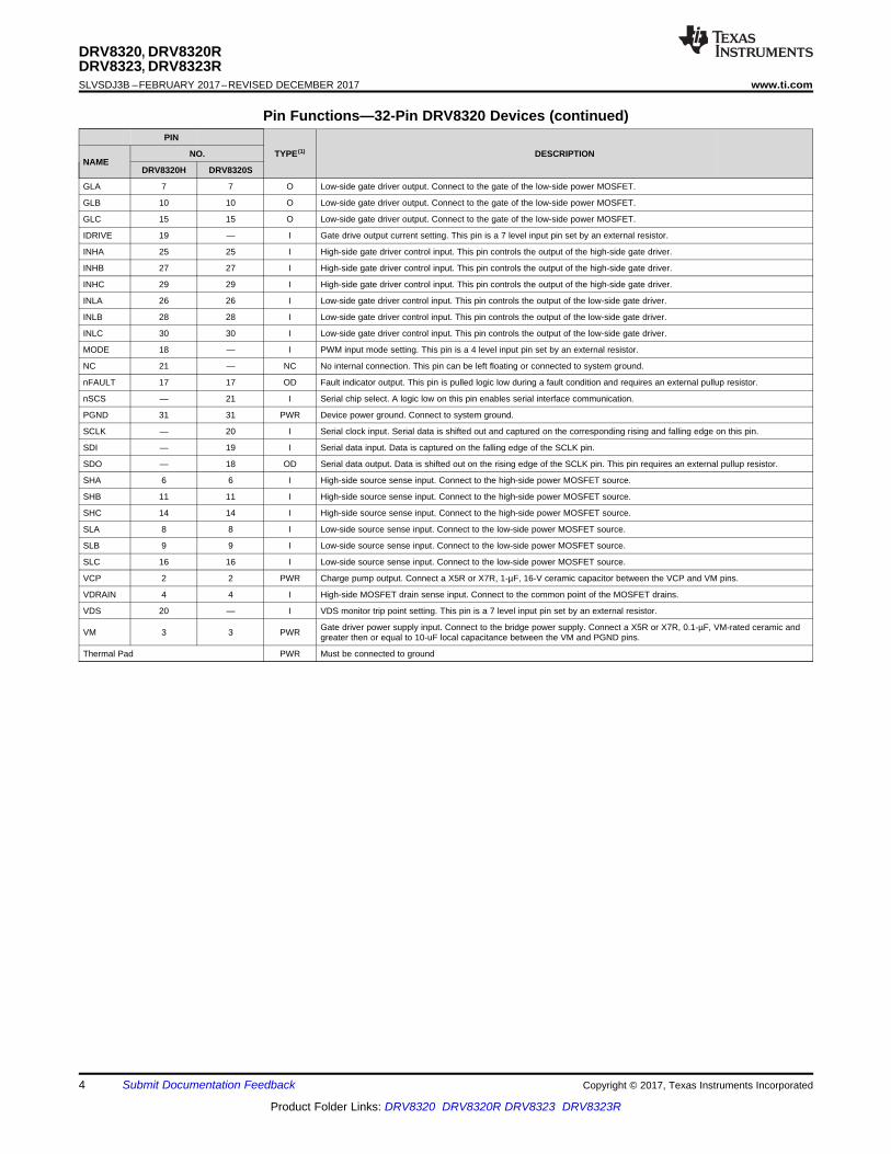
Pin Functions—32-Pin DRV8320 Devices (continued)PIN
TYPE (1) DESCRIPTIONNAME
NO.
DRV8320H DRV8320S
GLA 7 7 O Low-side gate driver output. Connect to the gate of the low-side power MOSFET.
GLB 10 10 O Low-side gate driver output. Connect to the gate of the low-side power MOSFET.
GLC 15 15 O Low-side gate driver output. Connect to the gate of the low-side power MOSFET.
IDRIVE 19 — I Gate drive output current setting. This pin is a 7 level input pin set by an external resistor.
INHA 25 25 I High-side gate driver control input. This pin controls the output of the high-side gate driver.
INHB 27 27 I High-side gate driver control input. This pin controls the output of the high-side gate driver.
INHC 29 29 I High-side gate driver control input. This pin controls the output of the high-side gate driver.
INLA 26 26 I Low-side gate driver control input. This pin controls the output of the low-side gate driver.
INLB 28 28 I Low-side gate driver control input. This pin controls the output of the low-side gate driver.
INLC 30 30 I Low-side gate driver control input. This pin controls the output of the low-side gate driver.
MODE 18 — I PWM input mode setting. This pin is a 4 level input pin set by an external resistor.
NC 21 — NC No internal connection. This pin can be left floating or connected to system ground.
nFAULT 17 17 OD Fault indicator output. This pin is pulled logic low during a fault condition and requires an external pullup resistor.
nSCS — 21 I Serial chip select. A logic low on this pin enables serial interface communication.
PGND 31 31 PWR Device power ground. Connect to system ground.
SCLK — 20 I Serial clock input. Serial data is shifted out and captured on the corresponding rising and falling edge on this pin.
SDI — 19 I Serial data input. Data is captured on the falling edge of the SCLK pin.
SDO — 18 OD Serial data output. Data is shifted out on the rising edge of the SCLK pin. This pin requires an external pullup resistor.
SHA 6 6 I High-side source sense input. Connect to the high-side power MOSFET source.
SHB 11 11 I High-side source sense input. Connect to the high-side power MOSFET source.
SHC 14 14 I High-side source sense input. Connect to the high-side power MOSFET source.
SLA 8 8 I Low-side source sense input. Connect to the low-side power MOSFET source.
SLB 9 9 I Low-side source sense input. Connect to the low-side power MOSFET source.
SLC 16 16 I Low-side source sense input. Connect to the low-side power MOSFET source.
VCP 2 2 PWR Charge pump output. Connect a X5R or X7R, 1-µF, 16-V ceramic capacitor between the VCP and VM pins.
VDRAIN 4 4 I High-side MOSFET drain sense input. Connect to the common point of the MOSFET drains.
VDS 20 — I VDS monitor trip point setting. This pin is a 7 level input pin set by an external resistor.
VM 3 3 PWR Gate driver power supply input. Connect to the bridge power supply. Connect a X5R or X7R, 0.1-µF, VM-rated ceramic andgreater then or equal to 10-uF local capacitance between the VM and PGND pins.
Thermal Pad PWR Must be connected to ground
40F
B11
SLB
1PGND 30 INHB
39nS
HD
N12
GLB
2CPL 29 INLA
38V
IN13
SH
B
3CPH 28 INHA
37N
C14
GH
B
4VCP 27 DVDD
36S
W15
GH
C
5VM 26 AGND
35C
B16
SH
C
6VDRAIN 25 ENABLE
34B
GN
D17
GLC
7GHA 24 NC
33IN
LC18
SLC
8SHA 23 VDS
32IN
HC
19G
ND
9GLA 22 IDRIVE
31IN
LB20
nFA
ULT
10SLA 21 MODE
Not to scale
Thermal
Pad
40F
B11
SLB
1PGND 30 INHB
39nS
HD
N12
GLB
2CPL 29 INLA
38V
IN13
SH
B
3CPH 28 INHA
37N
C14
GH
B
4VCP 27 DVDD
36S
W15
GH
C
5VM 26 AGND
35C
B16
SH
C
6VDRAIN 25 ENABLE
34B
GN
D17
GLC
7GHA 24 nSCS
33IN
LC18
SLC
8SHA 23 SCLK
32IN
HC
19G
ND
9GLA 22 SDI
31IN
LB20
nFA
ULT
10SLA 21 SDO
Not to scale
Thermal
Pad
5
DRV8320, DRV8320RDRV8323, DRV8323R
www.ti.com SLVSDJ3B –FEBRUARY 2017–REVISED DECEMBER 2017
Product Folder Links: DRV8320 DRV8320R DRV8323 DRV8323R
Submit Documentation FeedbackCopyright © 2017, Texas Instruments Incorporated
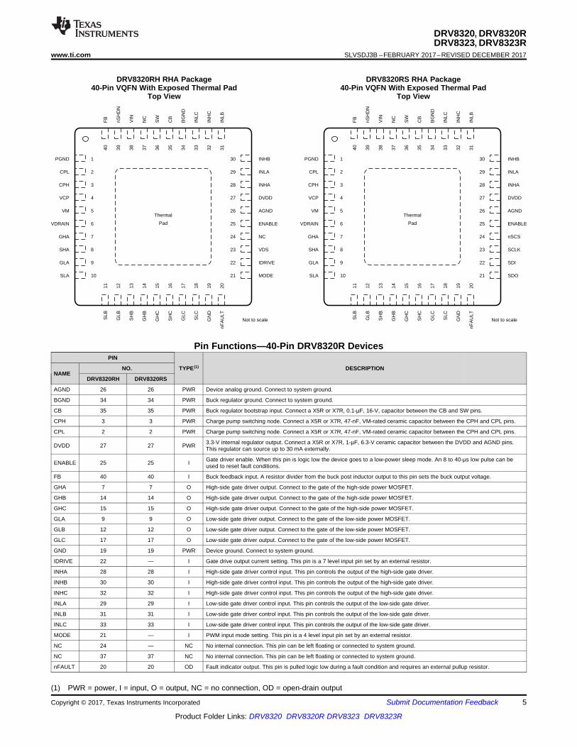
DRV8320RH RHA Package40-Pin VQFN With Exposed Thermal Pad
Top View
DRV8320RS RHA Package40-Pin VQFN With Exposed Thermal Pad
Top View
(1) PWR = power, I = input, O = output, NC = no connection, OD = open-drain output
Pin Functions—40-Pin DRV8320R DevicesPIN
TYPE (1) DESCRIPTIONNAME
NO.
DRV8320RH DRV8320RS
AGND 26 26 PWR Device analog ground. Connect to system ground.
BGND 34 34 PWR Buck regulator ground. Connect to system ground.
CB 35 35 PWR Buck regulator bootstrap input. Connect a X5R or X7R, 0.1-µF, 16-V, capacitor between the CB and SW pins.
CPH 3 3 PWR Charge pump switching node. Connect a X5R or X7R, 47-nF, VM-rated ceramic capacitor between the CPH and CPL pins.
CPL 2 2 PWR Charge pump switching node. Connect a X5R or X7R, 47-nF, VM-rated ceramic capacitor between the CPH and CPL pins.
DVDD 27 27 PWR 3.3-V internal regulator output. Connect a X5R or X7R, 1-µF, 6.3-V ceramic capacitor between the DVDD and AGND pins.This regulator can source up to 30 mA externally.
ENABLE 25 25 I Gate driver enable. When this pin is logic low the device goes to a low-power sleep mode. An 8 to 40-µs low pulse can beused to reset fault conditions.
FB 40 40 I Buck feedback input. A resistor divider from the buck post inductor output to this pin sets the buck output voltage.
GHA 7 7 O High-side gate driver output. Connect to the gate of the high-side power MOSFET.
GHB 14 14 O High-side gate driver output. Connect to the gate of the high-side power MOSFET.
GHC 15 15 O High-side gate driver output. Connect to the gate of the high-side power MOSFET.
GLA 9 9 O Low-side gate driver output. Connect to the gate of the low-side power MOSFET.
GLB 12 12 O Low-side gate driver output. Connect to the gate of the low-side power MOSFET.
GLC 17 17 O Low-side gate driver output. Connect to the gate of the low-side power MOSFET.
GND 19 19 PWR Device ground. Connect to system ground.
IDRIVE 22 — I Gate drive output current setting. This pin is a 7 level input pin set by an external resistor.
INHA 28 28 I High-side gate driver control input. This pin controls the output of the high-side gate driver.
INHB 30 30 I High-side gate driver control input. This pin controls the output of the high-side gate driver.
INHC 32 32 I High-side gate driver control input. This pin controls the output of the high-side gate driver.
INLA 29 29 I Low-side gate driver control input. This pin controls the output of the low-side gate driver.
INLB 31 31 I Low-side gate driver control input. This pin controls the output of the low-side gate driver.
INLC 33 33 I Low-side gate driver control input. This pin controls the output of the low-side gate driver.
MODE 21 — I PWM input mode setting. This pin is a 4 level input pin set by an external resistor.
NC 24 — NC No internal connection. This pin can be left floating or connected to system ground.
NC 37 37 NC No internal connection. This pin can be left floating or connected to system ground.
nFAULT 20 20 OD Fault indicator output. This pin is pulled logic low during a fault condition and requires an external pullup resistor.
40P
GN
D11
SN
B
1CPL 30 ENABLE
39IN
LC12
SP
B
2CPH 29 nSCS
38IN
HC
13G
LB
3VCP 28 SCLK
37IN
LB14
SH
B
4VM 27 SDI
36IN
HB
15G
HB
5VDRAIN 26 SDO
35IN
LA16
GH
C
6GHA 25 nFAULT
34IN
HA
17S
HC
7SHA 24 VREF
33D
VD
D18
GLC
8GLA 23 SOA
32A
GN
D19
SP
C
9SPA 22 SOB
31C
AL
20S
NC
10SNA 21 SOC
Not to scale
Thermal
Pad
40P
GN
D11
SN
B
1CPL 30 ENABLE
39IN
LC12
SP
B
2CPH 29 GAIN
38IN
HC
13G
LB
3VCP 28 VDS
37IN
LB14
SH
B
4VM 27 IDRIVE
36IN
HB
15G
HB
5VDRAIN 26 MODE
35IN
LA16
GH
C
6GHA 25 nFAULT
34IN
HA
17S
HC
7SHA 24 VREF
33D
VD
D18
GLC
8GLA 23 SOA
32A
GN
D19
SP
C
9SPA 22 SOB
31C
AL
20S
NC
10SNA 21 SOC
Not to scale
Thermal
Pad
6
DRV8320, DRV8320RDRV8323, DRV8323RSLVSDJ3B –FEBRUARY 2017–REVISED DECEMBER 2017 www.ti.com
Product Folder Links: DRV8320 DRV8320R DRV8323 DRV8323R
Submit Documentation Feedback Copyright © 2017, Texas Instruments Incorporated
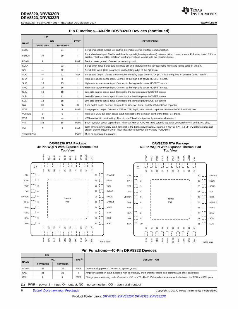
Pin Functions—40-Pin DRV8320R Devices (continued)PIN
TYPE (1) DESCRIPTIONNAME
NO.
DRV8320RH DRV8320RS
nSCS — 24 I Serial chip select. A logic low on this pin enables serial interface communication.
nSHDN 39 39 I Buck shutdown input. Enable and disable input (high voltage tolerant). Internal pullup current source. Pull lower than 1.25 V todisable. Float to enable. Establish input undervoltage lockout with two resistor divider.
PGND 1 1 PWR Device power ground. Connect to system ground.
SCLK — 23 I Serial clock input. Serial data is shifted out and captured on the corresponding rising and falling edge on this pin.
SDI — 22 I Serial data input. Data is captured on the falling edge of the SCLK pin.
SDO — 21 OD Serial data output. Data is shifted out on the rising edge of the SCLK pin. This pin requires an external pullup resistor.
SHA 8 8 I High-side source sense input. Connect to the high-side power MOSFET source.
SHB 13 13 I High-side source sense input. Connect to the high-side power MOSFET source.
SHC 16 16 I High-side source sense input. Connect to the high-side power MOSFET source.
SLA 10 10 I Low-side source sense input. Connect to the low-side power MOSFET source.
SLB 11 11 I Low-side source sense input. Connect to the low-side power MOSFET source.
SLC 18 18 I Low-side source sense input. Connect to the low-side power MOSFET source.
SW 36 36 O Buck switch node. Connect this pin to an inductor, diode, and the CB bootstrap capacitor.
VCP 4 4 PWR Charge pump output. Connect a X5R or X7R, 1-µF, 16-V ceramic capacitor between the VCP and VM pins.
VDRAIN 6 6 I High-side MOSFET drain sense input. Connect to the common point of the MOSFET drains.
VDS 23 — I VDS monitor trip point setting. This pin is a 7 level input pin set by an external resistor.
VIN 38 38 PWR Buck regulator power supply input. Place an X5R or X7R, VM-rated ceramic capacitor between the VIN and BGND pins.
VM 5 5 PWR Gate driver power supply input. Connect to the bridge power supply. Connect a X5R or X7R, 0.1-µF, VM-rated ceramic andgreater then or equal to 10-uF local capacitance between the VM and PGND pins.
Thermal Pad PWR Must be connected to ground
DRV8323H RTA Package40-Pin WQFN With Exposed Thermal Pad
Top View
DRV8323S RTA Package40-Pin WQFN With Exposed Thermal Pad
Top View
(1) PWR = power, I = input, O = output, NC = no connection, OD = open-drain output
Pin Functions—40-Pin DRV8323 DevicesPIN
TYPE (1) DESCRIPTIONNAME
NO.
DRV8323H DRV8323S
AGND 32 32 PWR Device analog ground. Connect to system ground.
CAL 31 31 I Amplifier calibration input. Set logic high to internally short amplifier inputs and perform auto offset calibration.
CPH 2 2 PWR Charge pump switching node. Connect a X5R or X7R, 47-nF, VM-rated ceramic capacitor between the CPH and CPL pins.
7
DRV8320, DRV8320RDRV8323, DRV8323R
www.ti.com SLVSDJ3B –FEBRUARY 2017–REVISED DECEMBER 2017
Product Folder Links: DRV8320 DRV8320R DRV8323 DRV8323R
Submit Documentation FeedbackCopyright © 2017, Texas Instruments Incorporated
Pin Functions—40-Pin DRV8323 Devices (continued)PIN
TYPE (1) DESCRIPTIONNAME
NO.
DRV8323H DRV8323S
CPL 1 1 PWR Charge pump switching node. Connect a X5R or X7R, 47-nF, VM-rated ceramic capacitor between the CPH and CPL pins.
DVDD 33 33 PWR R 3.3-V internal regulator output. Connect a X5R or X7R, 1-µF, 6.3-V ceramic capacitor between the DVDD and AGND pins.This regulator can source up to 30 mA externally.
ENABLE 30 30 I Gate driver enable. When this pin is logic low the device goes to a low-power sleep mode. An 8 to 40-µs low pulse can beused to reset fault conditions.
GAIN 29 — I Amplifier gain setting. The pin is a 4 level input pin set by an external resistor.
GHA 6 6 O High-side gate driver output. Connect to the gate of the high-side power MOSFET.
GHB 15 15 O High-side gate driver output. Connect to the gate of the high-side power MOSFET.
GHC 16 16 O High-side gate driver output. Connect to the gate of the high-side power MOSFET.
GLA 8 8 O Low-side gate driver output. Connect to the gate of the low-side power MOSFET.
GLB 13 13 O Low-side gate driver output. Connect to the gate of the low-side power MOSFET.
GLC 18 18 O Low-side gate driver output. Connect to the gate of the low-side power MOSFET.
IDRIVE 27 — I Gate drive output current setting. This pin is a 7 level input pin set by an external resistor.
INHA 34 34 I High-side gate driver control input. This pin controls the output of the high-side gate driver.
INHB 36 36 I High-side gate driver control input. This pin controls the output of the high-side gate driver.
INHC 38 38 I High-side gate driver control input. This pin controls the output of the high-side gate driver.
INLA 35 35 I Low-side gate driver control input. This pin controls the output of the low-side gate driver.
INLB 37 37 I Low-side gate driver control input. This pin controls the output of the low-side gate driver.
INLC 39 39 I Low-side gate driver control input. This pin controls the output of the low-side gate driver.
MODE 26 — I PWM input mode setting. This pin is a 4 level input pin set by an external resistor.
nFAULT 25 25 OD Fault indicator output. This pin is pulled logic low during a fault condition and requires an external pullup resistor.
nSCS — 29 I Serial chip select. A logic low on this pin enables serial interface communication.
PGND 40 40 PWR Device power ground. Connect to system ground.
SCLK — 28 I Serial clock input. Serial data is shifted out and captured on the corresponding rising and falling edge on this pin.
SDI — 27 I Serial data input. Data is captured on the falling edge of the SCLK pin.
SDO — 26 OD Serial data output. Data is shifted out on the rising edge of the SCLK pin. This pin requires an external pullup resistor.
SHA 7 7 I High-side source sense input. Connect to the high-side power MOSFET source.
SHB 14 14 I High-side source sense input. Connect to the high-side power MOSFET source.
SHC 17 17 I High-side source sense input. Connect to the high-side power MOSFET source.
SNA 10 10 I Current sense amplifier input. Connect to the low-side of the current shunt resistor.
SNB 11 11 I Current sense amplifier input. Connect to the low-side of the current shunt resistor.
SNC 20 20 I Current sense amplifier input. Connect to the low-side of the current shunt resistor.
SOA 23 23 O Current sense amplifier output.
SOB 22 22 O Current sense amplifier output.
SOC 21 21 O Current sense amplifier output.
SPA 9 9 I Low-side current shunt amplifier input. Connect to the low-side power MOSFET source and high-side of the current shuntresistor.
SPB 12 12 I Low-side current shunt amplifier input. Connect to the low-side power MOSFET source and high-side of the current shuntresistor.
SPC 19 19 I Low-side current shunt amplifier input. Connect to the low-side power MOSFET source and high-side of the current shuntresistor.
VCP 3 3 PWR Charge pump output. Connect a X5R or X7R, 1-µF, 16-V ceramic capacitor between the VCP and VM pins.
VDRAIN 5 5 I High-side MOSFET drain sense input. Connect to the common point of the MOSFET drains.
VDS 28 — I VDS monitor trip point setting. This pin is a 7 level input pin set by an external resistor.
VM 4 4 PWR Gate driver power supply input. Connect to the bridge power supply. Connect a X5R or X7R, 0.1-µF, VM-rated ceramic andgreater then or equal to 10-uF local capacitance between the VM and PGND pins.
VREF 24 24 PWR Current sense amplifier power supply input and reference. Connect a X5R or X7R, 0.1-µF, 6.3-V ceramic capacitor betweenthe VREF and AGND pins.
Thermal Pad PWR Must be connected to ground
48nS
HD
N13
SN
B
1FB 36 DVDD
47V
IN14
SP
B
2PGND 35 AGND
46N
C15
GLB
3CPL 34 CAL
45S
W16
SH
B
4CPH 33 ENABLE
44C
B17
GH
B
5VCP 32 GAIN
43B
GN
D18
GH
C
6VM 31 VDS
42IN
LC19
SH
C
7VDRAIN 30 IDRIVE
41IN
HC
20G
LC
8GHA 29 MODE
40IN
LB21
SP
C
9SHA 28 nFAULT
39IN
HB
22S
NC
10GLA 27 DGND
38IN
LA23
SO
C
11SPA 26 VREF
37IN
HA
24S
OB
12SNA 25 SOA
Not to scale
Thermal
Pad
48nS
HD
N13
SN
B
1FB 36 DVDD
47V
IN14
SP
B
2PGND 35 AGND
46N
C15
GLB
3CPL 34 CAL
45S
W16
SH
B
4CPH 33 ENABLE
44C
B17
GH
B
5VCP 32 nSCS
43B
GN
D18
GH
C
6VM 31 SCLK
42IN
LC19
SH
C
7VDRAIN 30 SDI
41IN
HC
20G
LC
8GHA 29 SDO
40IN
LB21
SP
C
9SHA 28 nFAULT
39IN
HB
22S
NC
10GLA 27 DGND
38IN
LA23
SO
C
11SPA 26 VREF
37IN
HA
24S
OB
12SNA 25 SOA
Not to scale
Thermal
Pad
8
DRV8320, DRV8320RDRV8323, DRV8323RSLVSDJ3B –FEBRUARY 2017–REVISED DECEMBER 2017 www.ti.com
Product Folder Links: DRV8320 DRV8320R DRV8323 DRV8323R
Submit Documentation Feedback Copyright © 2017, Texas Instruments Incorporated
DRV8323RH RGZ Package48-Pin VQFN With Exposed Thermal Pad
Top View
DRV8323RS RGZ Package48-Pin VQFN With Exposed Thermal Pad
Top View
(1) PWR = power, I = input, O = output, NC = no connection, OD = open-drain output
Pin Functions—48-Pin DRV8323R DevicesPIN
TYPE (1) DESCRIPTIONNAME
NO.
DRV8323RH DRV8323RS
AGND 35 35 PWR Device analog ground. Connect to system ground.
BGND 43 43 PWR Buck regulator ground. Connect to system ground.
CAL 34 34 I Amplifier calibration input. Set logic high to internally short amplifier inputs and perform auto offset calibration.
CB 44 44 PWR Buck regulator bootstrap input. Connect a X5R or X7R, 0.1-µF, 16-V, capacitor between the CB and SW pins.
CPH 4 4 PWR Charge pump switching node. Connect a X5R or X7R, 47-nF, VM-rated ceramic capacitor between the CPH and CPL pins.
CPL 3 3 PWR Charge pump switching node. Connect a X5R or X7R, 47-nF, VM-rated ceramic capacitor between the CPH and CPL pins.
DGND 27 27 PWR Device ground. Connect to system ground.
DVDD 36 36 PWR 3.3-V internal regulator output. Connect a X5R or X7R, 1-µF, 6.3-V ceramic capacitor between the DVDD and AGND pins.This regulator can source up to 30 mA externally.
ENABLE 33 33 I Gate driver enable. When this pin is logic low the device goes to a low-power sleep mode. An 8 to 40-µs low pulse can beused to reset fault conditions.
FB 1 1 I Buck feedback input. A resistor divider from the buck post inductor output to this pin sets the buck output voltage.
GAIN 32 — I Amplifier gain setting. The pin is a 4 level input pin set by an external resistor.
GHA 8 8 O High-side gate driver output. Connect to the gate of the high-side power MOSFET.
GHB 17 17 O High-side gate driver output. Connect to the gate of the high-side power MOSFET.
GHC 18 18 O High-side gate driver output. Connect to the gate of the high-side power MOSFET.
GLA 10 10 O Low-side gate driver output. Connect to the gate of the low-side power MOSFET.
GLB 15 15 O Low-side gate driver output. Connect to the gate of the low-side power MOSFET.
GLC 20 20 O Low-side gate driver output. Connect to the gate of the low-side power MOSFET.
IDRIVE 30 — I Gate drive output current setting. This pin is a 7 level input pin set by an external resistor.
INHA 37 37 I High-side gate driver control input. This pin controls the output of the high-side gate driver.
INHB 39 39 I High-side gate driver control input. This pin controls the output of the high-side gate driver.
INHC 41 41 I High-side gate driver control input. This pin controls the output of the high-side gate driver.
INLA 38 38 I Low-side gate driver control input. This pin controls the output of the low-side gate driver.
INLB 40 40 I Low-side gate driver control input. This pin controls the output of the low-side gate driver.
INLC 42 42 I Low-side gate driver control input. This pin controls the output of the low-side gate driver.
MODE 29 — I PWM input mode setting. This pin is a 4 level input pin set by an external resistor.
NC 46 46 NC No internal connection. This pin can be left floating or connected to system ground.
nFAULT 28 28 OD Fault indicator output. This pin is pulled logic low during a fault condition and requires an external pullup resistor.
9
DRV8320, DRV8320RDRV8323, DRV8323R
www.ti.com SLVSDJ3B –FEBRUARY 2017–REVISED DECEMBER 2017
Product Folder Links: DRV8320 DRV8320R DRV8323 DRV8323R
Submit Documentation FeedbackCopyright © 2017, Texas Instruments Incorporated
Pin Functions—48-Pin DRV8323R Devices (continued)PIN
TYPE (1) DESCRIPTIONNAME
NO.
DRV8323RH DRV8323RS
nSCS — 32 I Serial chip select. A logic low on this pin enables serial interface communication.
nSHDN 48 48 I Buck shutdown input. Enable and disable input (high voltage tolerant). Internal pullup current source. Pull lower than 1.25 Vto disable. Float to enable. Establish input undervoltage lockout with two resistor divider.
PGND 2 2 PWR Device power ground. Connect to system ground.
SCLK — 31 I Serial clock input. Serial data is shifted out and captured on the corresponding rising and falling edge on this pin.
SDI — 30 I Serial data input. Data is captured on the falling edge of the SCLK pin.
SDO — 29 OD Serial data output. Data is shifted out on the rising edge of the SCLK pin. This pin requires an external pullup resistor.
SHA 9 9 I High-side source sense input. Connect to the high-side power MOSFET source.
SHB 16 16 I High-side source sense input. Connect to the high-side power MOSFET source.
SHC 19 19 I High-side source sense input. Connect to the high-side power MOSFET source.
SNA 12 12 I Current sense amplifier input. Connect to the low-side of the current shunt resistor.
SNB 13 13 I Current sense amplifier input. Connect to the low-side of the current shunt resistor.
SNC 22 22 I Current sense amplifier input. Connect to the low-side of the current shunt resistor.
SOA 25 25 O Current sense amplifier output.
SOB 24 24 O Current sense amplifier output.
SOC 23 23 O Current sense amplifier output.
SPA 11 11 I Low-side current shunt amplifier input. Connect to the low-side power MOSFET source and high-side of the current shuntresistor.
SPB 14 14 I Low-side current shunt amplifier input. Connect to the low-side power MOSFET source and high-side of the current shuntresistor.
SPC 21 21 I Low-side current shunt amplifier input. Connect to the low-side power MOSFET source and high-side of the current shuntresistor.
SW 45 45 O Buck switch node. Connect this pin to an inductor, diode, and the CB bootstrap capacitor.
VCP 5 5 PWR Charge pump output. Connect a X5R or X7R, 1-µF, 16-V ceramic capacitor between the VCP and VM pins.
VDRAIN 7 7 I High-side MOSFET drain sense input. Connect to the common point of the MOSFET drains.
VDS 31 — I VDS monitor trip point setting. This pin is a 7 level input pin set by an external resistor.
VIN 47 47 PWR Buck regulator power supply input. Place an X5R or X7R, VM-rated ceramic capacitor between the VIN and BGND pins.
VM 6 6 PWR Gate driver power supply input. Connect to the bridge power supply. Connect a X5R or X7R, 0.1-µF, VM-rated ceramic andgreater then or equal to 10-uF local capacitance between the VM and PGND pins.
VREF 26 26 PWR Current sense amplifier power supply input and reference. Connect a X5R or X7R, 0.1-µF, 6.3-V ceramic capacitor betweenthe VREF and AGND pins.
Thermal Pad PWR Must be connected to ground
10
DRV8320, DRV8320RDRV8323, DRV8323RSLVSDJ3B –FEBRUARY 2017–REVISED DECEMBER 2017 www.ti.com
Product Folder Links: DRV8320 DRV8320R DRV8323 DRV8323R
Submit Documentation Feedback Copyright © 2017, Texas Instruments Incorporated
(1) Stresses beyond those listed under Absolute Maximum Ratings may cause permanent damage to the device. These are stress ratingsonly, which do not imply functional operation of the device at these or any other conditions beyond those indicated under RecommendedOperating Conditions. Exposure to absolute-maximum-rated conditions for extended periods may affect device reliability.
(2) Continuous high-side gate pin (GHx) and phase node pin voltage (SHx) should be limited to –2 V minimum for an absolute maximum of65 V on VM. At 60 V and lower, the full specification of –5 V continuous on GHx and SHx is allowable.
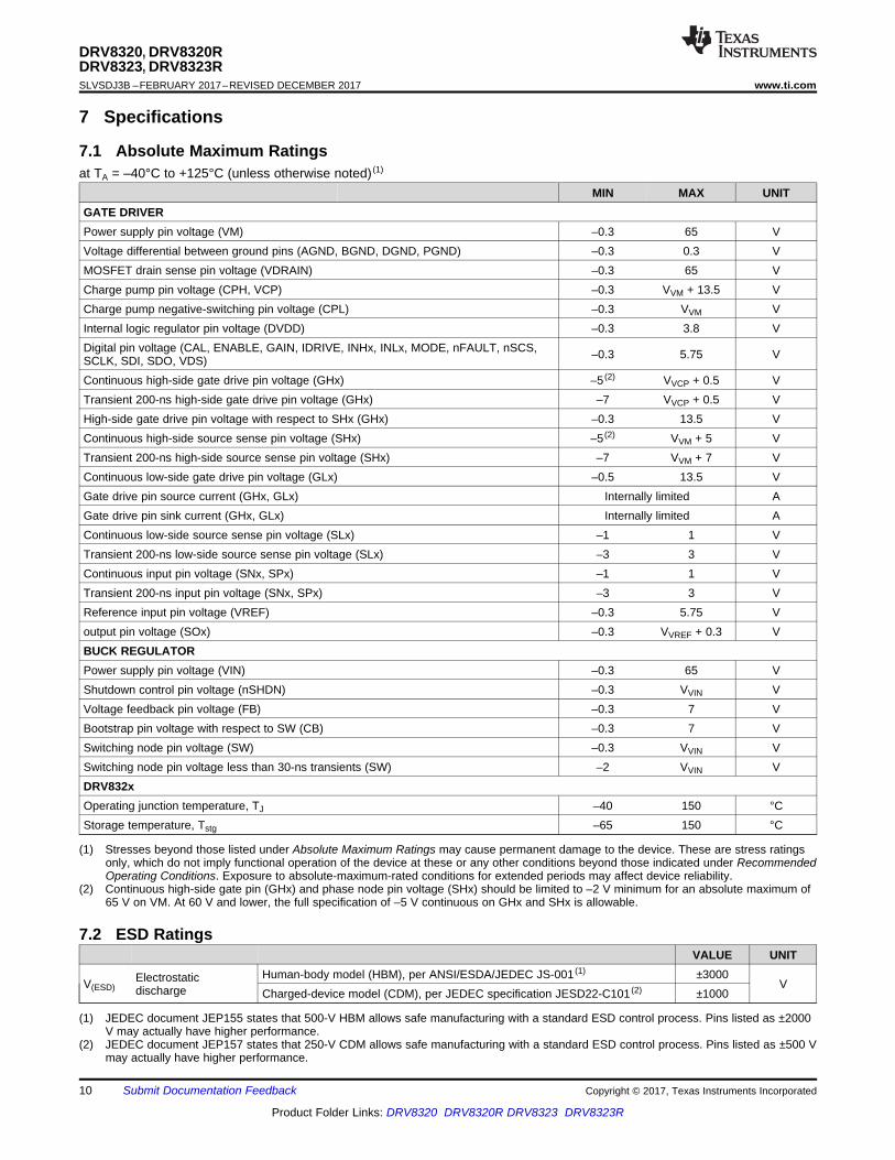
7 Specifications
7.1 Absolute Maximum Ratingsat TA = –40°C to +125°C (unless otherwise noted) (1)
MIN MAX UNITGATE DRIVERPower supply pin voltage (VM) –0.3 65 VVoltage differential between ground pins (AGND, BGND, DGND, PGND) –0.3 0.3 VMOSFET drain sense pin voltage (VDRAIN) –0.3 65 VCharge pump pin voltage (CPH, VCP) –0.3 VVM + 13.5 VCharge pump negative-switching pin voltage (CPL) –0.3 VVM VInternal logic regulator pin voltage (DVDD) –0.3 3.8 VDigital pin voltage (CAL, ENABLE, GAIN, IDRIVE, INHx, INLx, MODE, nFAULT, nSCS,SCLK, SDI, SDO, VDS) –0.3 5.75 V
Continuous high-side gate drive pin voltage (GHx) –5 (2) VVCP + 0.5 VTransient 200-ns high-side gate drive pin voltage (GHx) –7 VVCP + 0.5 VHigh-side gate drive pin voltage with respect to SHx (GHx) –0.3 13.5 VContinuous high-side source sense pin voltage (SHx) –5 (2) VVM + 5 VTransient 200-ns high-side source sense pin voltage (SHx) –7 VVM + 7 VContinuous low-side gate drive pin voltage (GLx) –0.5 13.5 VGate drive pin source current (GHx, GLx) Internally limited AGate drive pin sink current (GHx, GLx) Internally limited AContinuous low-side source sense pin voltage (SLx) –1 1 VTransient 200-ns low-side source sense pin voltage (SLx) –3 3 VContinuous input pin voltage (SNx, SPx) –1 1 VTransient 200-ns input pin voltage (SNx, SPx) –3 3 VReference input pin voltage (VREF) –0.3 5.75 Voutput pin voltage (SOx) –0.3 VVREF + 0.3 VBUCK REGULATORPower supply pin voltage (VIN) –0.3 65 VShutdown control pin voltage (nSHDN) –0.3 VVIN VVoltage feedback pin voltage (FB) –0.3 7 VBootstrap pin voltage with respect to SW (CB) –0.3 7 VSwitching node pin voltage (SW) –0.3 VVIN VSwitching node pin voltage less than 30-ns transients (SW) –2 VVIN VDRV832xOperating junction temperature, TJ –40 150 °CStorage temperature, Tstg –65 150 °C
(1) JEDEC document JEP155 states that 500-V HBM allows safe manufacturing with a standard ESD control process. Pins listed as ±2000V may actually have higher performance.
(2) JEDEC document JEP157 states that 250-V CDM allows safe manufacturing with a standard ESD control process. Pins listed as ±500 Vmay actually have higher performance.
7.2 ESD RatingsVALUE UNIT
V(ESD)Electrostaticdischarge
Human-body model (HBM), per ANSI/ESDA/JEDEC JS-001 (1) ±3000V
Charged-device model (CDM), per JEDEC specification JESD22-C101 (2) ±1000

11
DRV8320, DRV8320RDRV8323, DRV8323R
www.ti.com SLVSDJ3B –FEBRUARY 2017–REVISED DECEMBER 2017
Product Folder Links: DRV8320 DRV8320R DRV8323 DRV8323R
Submit Documentation FeedbackCopyright © 2017, Texas Instruments Incorporated
(1) Power dissipation and thermal limits must be observed
7.3 Recommended Operating Conditionsat TA = –40°C to +125°C (unless otherwise noted)
MIN MAX UNITGATE DRIVERVVM Power supply voltage (VM) 6 60 V
VIInput voltage (CAL, ENABLE, GAIN, IDRIVE, INHx, INLx, MODE, nSCS,SCLK, SDI, VDS) 0 5.5 V
fPWM Applied PWM signal (INHx, INLx) 0 200 (1) kHzIGATE_HS High-side average gate drive current (GHx) 0 25 (1) mAIGATE_LS Low-side average gate drive current (GLx) 0 25 (1) mAIDVDD External load current (DVDD) 0 30 (1) mAVVREF Reference voltage input (VREF) 3 5.5 VISO output current (SOx) 0 5 mAVOD Open drain pullup voltage (nFAULT, SDO) 0 5.5 VIOD Open drain output current (nFAULT, SDO) 0 5 mABUCK REGULATORVVIN Power supply voltage (VIN) 4 60 VVnSHDN Shutdown control input voltage (nSHDN) 0 60 VDRV832xTA Operating ambient temperature –40 125 °C
(1) For more information about traditional and new thermal metrics, see the Semiconductor and IC Package Thermal Metrics applicationreport.
7.4 Thermal Information
THERMAL METRIC (1)
DRV832x
UNITRTV(WQFN)
RHA(VQFN)
RTA(WQFN)
RGZ(VQFN)
32 PINS 40 PINS 40 PINS 48 PINSRθJA Junction-to-ambient thermal resistance 32.9 30.1 32.1 26.6 °C/WRθJC(top) Junction-to-case (top) thermal resistance 15.8 16.7 11 13.9 °C/WRθJB Junction-to-board thermal resistance 6.8 9.9 7.1 9.2 °C/WψJT Junction-to-top characterization parameter 0.2 0.5 0.1 0.3 °C/WψJB Junction-to-board characterization parameter 6.8 9.9 7.1 9.1 °C/WRθJC(bot) Junction-to-case (bottom) thermal resistance 2.1 2.2 2.1 2 °C/W
12
DRV8320, DRV8320RDRV8323, DRV8323RSLVSDJ3B –FEBRUARY 2017–REVISED DECEMBER 2017 www.ti.com
Product Folder Links: DRV8320 DRV8320R DRV8323 DRV8323R
Submit Documentation Feedback Copyright © 2017, Texas Instruments Incorporated
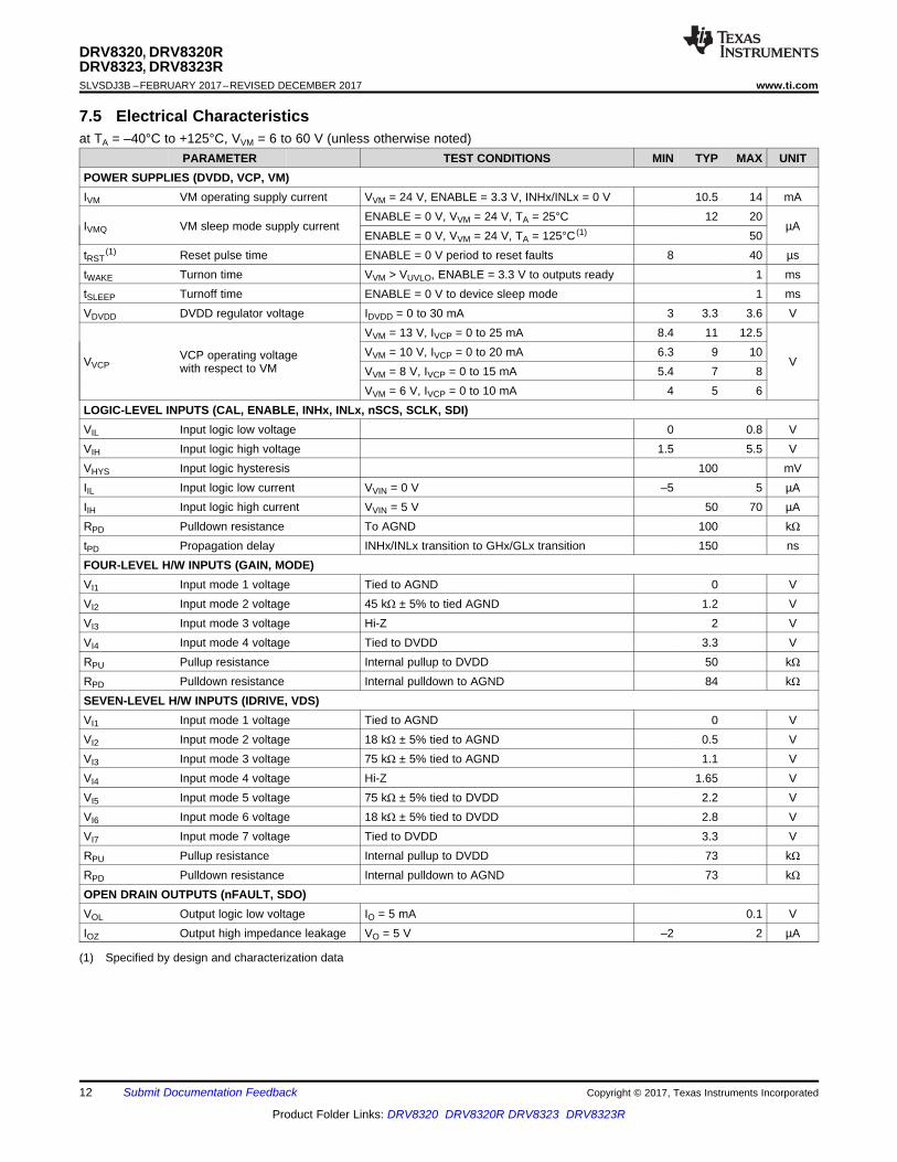
(1) Specified by design and characterization data
7.5 Electrical Characteristicsat TA = –40°C to +125°C, VVM = 6 to 60 V (unless otherwise noted)
PARAMETER TEST CONDITIONS MIN TYP MAX UNITPOWER SUPPLIES (DVDD, VCP, VM)IVM VM operating supply current VVM = 24 V, ENABLE = 3.3 V, INHx/INLx = 0 V 10.5 14 mA
IVMQ VM sleep mode supply currentENABLE = 0 V, VVM = 24 V, TA = 25°C 12 20
µAENABLE = 0 V, VVM = 24 V, TA = 125°C (1) 50
tRST(1) Reset pulse time ENABLE = 0 V period to reset faults 8 40 µs
tWAKE Turnon time VVM > VUVLO, ENABLE = 3.3 V to outputs ready 1 mstSLEEP Turnoff time ENABLE = 0 V to device sleep mode 1 msVDVDD DVDD regulator voltage IDVDD = 0 to 30 mA 3 3.3 3.6 V
VVCPVCP operating voltagewith respect to VM
VVM = 13 V, IVCP = 0 to 25 mA 8.4 11 12.5
VVVM = 10 V, IVCP = 0 to 20 mA 6.3 9 10VVM = 8 V, IVCP = 0 to 15 mA 5.4 7 8VVM = 6 V, IVCP = 0 to 10 mA 4 5 6
LOGIC-LEVEL INPUTS (CAL, ENABLE, INHx, INLx, nSCS, SCLK, SDI)VIL Input logic low voltage 0 0.8 VVIH Input logic high voltage 1.5 5.5 VVHYS Input logic hysteresis 100 mVIIL Input logic low current VVIN = 0 V –5 5 µAIIH Input logic high current VVIN = 5 V 50 70 µARPD Pulldown resistance To AGND 100 kΩtPD Propagation delay INHx/INLx transition to GHx/GLx transition 150 nsFOUR-LEVEL H/W INPUTS (GAIN, MODE)VI1 Input mode 1 voltage Tied to AGND 0 VVI2 Input mode 2 voltage 45 kΩ ± 5% to tied AGND 1.2 VVI3 Input mode 3 voltage Hi-Z 2 VVI4 Input mode 4 voltage Tied to DVDD 3.3 VRPU Pullup resistance Internal pullup to DVDD 50 kΩRPD Pulldown resistance Internal pulldown to AGND 84 kΩSEVEN-LEVEL H/W INPUTS (IDRIVE, VDS)VI1 Input mode 1 voltage Tied to AGND 0 VVI2 Input mode 2 voltage 18 kΩ ± 5% tied to AGND 0.5 VVI3 Input mode 3 voltage 75 kΩ ± 5% tied to AGND 1.1 VVI4 Input mode 4 voltage Hi-Z 1.65 VVI5 Input mode 5 voltage 75 kΩ ± 5% tied to DVDD 2.2 VVI6 Input mode 6 voltage 18 kΩ ± 5% tied to DVDD 2.8 VVI7 Input mode 7 voltage Tied to DVDD 3.3 VRPU Pullup resistance Internal pullup to DVDD 73 kΩRPD Pulldown resistance Internal pulldown to AGND 73 kΩOPEN DRAIN OUTPUTS (nFAULT, SDO)VOL Output logic low voltage IO = 5 mA 0.1 VIOZ Output high impedance leakage VO = 5 V –2 2 µA
13
DRV8320, DRV8320RDRV8323, DRV8323R
www.ti.com SLVSDJ3B –FEBRUARY 2017–REVISED DECEMBER 2017
Product Folder Links: DRV8320 DRV8320R DRV8323 DRV8323R
Submit Documentation FeedbackCopyright © 2017, Texas Instruments Incorporated
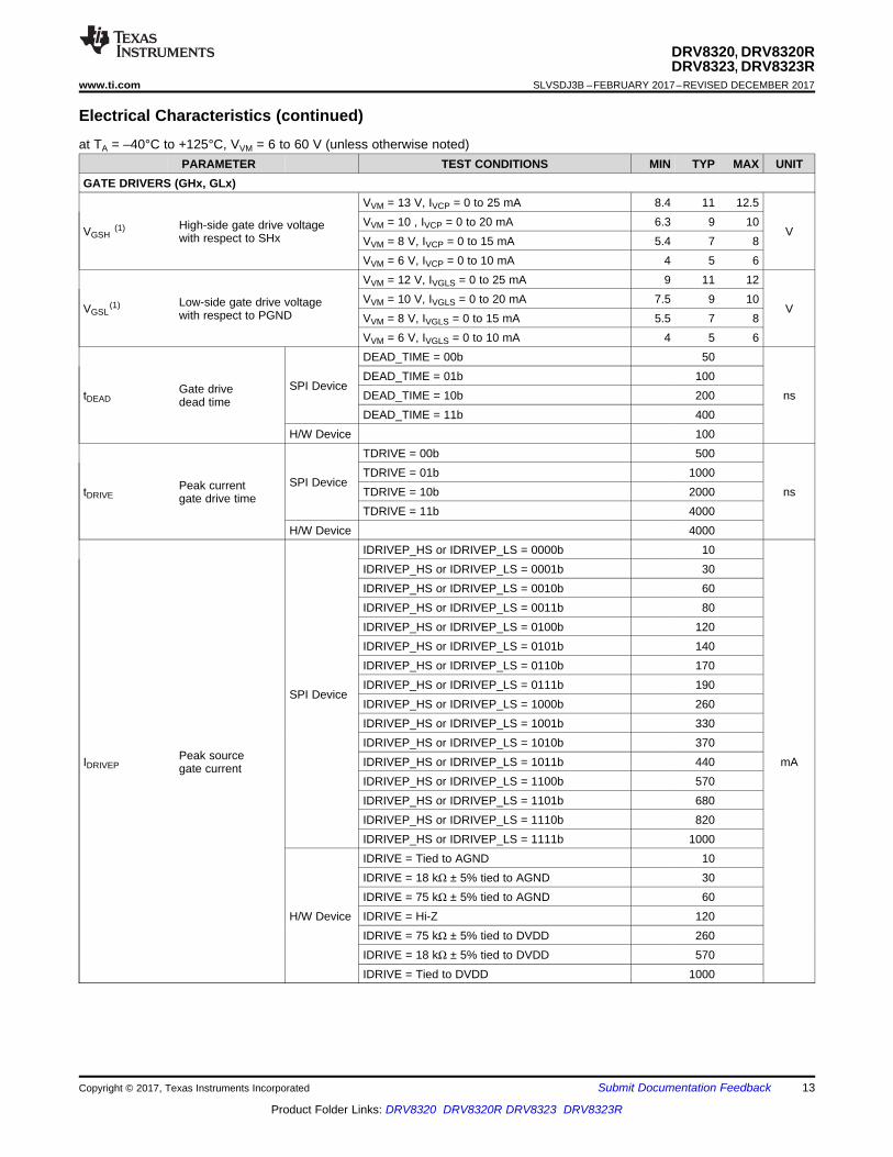
Electrical Characteristics (continued)at TA = –40°C to +125°C, VVM = 6 to 60 V (unless otherwise noted)
PARAMETER TEST CONDITIONS MIN TYP MAX UNITGATE DRIVERS (GHx, GLx)
VGSH(1) High-side gate drive voltage
with respect to SHx
VVM = 13 V, IVCP = 0 to 25 mA 8.4 11 12.5
VVVM = 10 , IVCP = 0 to 20 mA 6.3 9 10VVM = 8 V, IVCP = 0 to 15 mA 5.4 7 8VVM = 6 V, IVCP = 0 to 10 mA 4 5 6
VGSL(1) Low-side gate drive voltage
with respect to PGND
VVM = 12 V, IVGLS = 0 to 25 mA 9 11 12
VVVM = 10 V, IVGLS = 0 to 20 mA 7.5 9 10VVM = 8 V, IVGLS = 0 to 15 mA 5.5 7 8VVM = 6 V, IVGLS = 0 to 10 mA 4 5 6
tDEADGate drivedead time
SPI Device
DEAD_TIME = 00b 50
nsDEAD_TIME = 01b 100DEAD_TIME = 10b 200DEAD_TIME = 11b 400
H/W Device 100
tDRIVEPeak currentgate drive time
SPI Device
TDRIVE = 00b 500
nsTDRIVE = 01b 1000TDRIVE = 10b 2000TDRIVE = 11b 4000
H/W Device 4000
IDRIVEPPeak sourcegate current
SPI Device
IDRIVEP_HS or IDRIVEP_LS = 0000b 10
mA
IDRIVEP_HS or IDRIVEP_LS = 0001b 30IDRIVEP_HS or IDRIVEP_LS = 0010b 60IDRIVEP_HS or IDRIVEP_LS = 0011b 80IDRIVEP_HS or IDRIVEP_LS = 0100b 120IDRIVEP_HS or IDRIVEP_LS = 0101b 140IDRIVEP_HS or IDRIVEP_LS = 0110b 170IDRIVEP_HS or IDRIVEP_LS = 0111b 190IDRIVEP_HS or IDRIVEP_LS = 1000b 260IDRIVEP_HS or IDRIVEP_LS = 1001b 330IDRIVEP_HS or IDRIVEP_LS = 1010b 370IDRIVEP_HS or IDRIVEP_LS = 1011b 440IDRIVEP_HS or IDRIVEP_LS = 1100b 570IDRIVEP_HS or IDRIVEP_LS = 1101b 680IDRIVEP_HS or IDRIVEP_LS = 1110b 820IDRIVEP_HS or IDRIVEP_LS = 1111b 1000
H/W Device
IDRIVE = Tied to AGND 10IDRIVE = 18 kΩ ± 5% tied to AGND 30IDRIVE = 75 kΩ ± 5% tied to AGND 60IDRIVE = Hi-Z 120IDRIVE = 75 kΩ ± 5% tied to DVDD 260IDRIVE = 18 kΩ ± 5% tied to DVDD 570IDRIVE = Tied to DVDD 1000
14
DRV8320, DRV8320RDRV8323, DRV8323RSLVSDJ3B –FEBRUARY 2017–REVISED DECEMBER 2017 www.ti.com
Product Folder Links: DRV8320 DRV8320R DRV8323 DRV8323R
Submit Documentation Feedback Copyright © 2017, Texas Instruments Incorporated
Electrical Characteristics (continued)at TA = –40°C to +125°C, VVM = 6 to 60 V (unless otherwise noted)
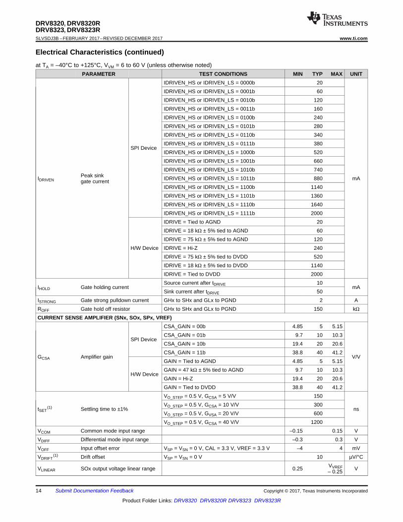
PARAMETER TEST CONDITIONS MIN TYP MAX UNIT
IDRIVENPeak sinkgate current
SPI Device
IDRIVEN_HS or IDRIVEN_LS = 0000b 20
mA
IDRIVEN_HS or IDRIVEN_LS = 0001b 60IDRIVEN_HS or IDRIVEN_LS = 0010b 120IDRIVEN_HS or IDRIVEN_LS = 0011b 160IDRIVEN_HS or IDRIVEN_LS = 0100b 240IDRIVEN_HS or IDRIVEN_LS = 0101b 280IDRIVEN_HS or IDRIVEN_LS = 0110b 340IDRIVEN_HS or IDRIVEN_LS = 0111b 380IDRIVEN_HS or IDRIVEN_LS = 1000b 520IDRIVEN_HS or IDRIVEN_LS = 1001b 660IDRIVEN_HS or IDRIVEN_LS = 1010b 740IDRIVEN_HS or IDRIVEN_LS = 1011b 880IDRIVEN_HS or IDRIVEN_LS = 1100b 1140IDRIVEN_HS or IDRIVEN_LS = 1101b 1360IDRIVEN_HS or IDRIVEN_LS = 1110b 1640IDRIVEN_HS or IDRIVEN_LS = 1111b 2000
H/W Device
IDRIVE = Tied to AGND 20IDRIVE = 18 kΩ ± 5% tied to AGND 60IDRIVE = 75 kΩ ± 5% tied to AGND 120IDRIVE = Hi-Z 240IDRIVE = 75 kΩ ± 5% tied to DVDD 520IDRIVE = 18 kΩ ± 5% tied to DVDD 1140IDRIVE = Tied to DVDD 2000
IHOLD Gate holding currentSource current after tDRIVE 10
mASink current after tDRIVE 50
ISTRONG Gate strong pulldown current GHx to SHx and GLx to PGND 2 AROFF Gate hold off resistor GHx to SHx and GLx to PGND 150 kΩCURRENT SENSE AMPLIFIER (SNx, SOx, SPx, VREF)
GCSA Amplifier gain
SPI Device
CSA_GAIN = 00b 4.85 5 5.15
V/V
CSA_GAIN = 01b 9.7 10 10.3CSA_GAIN = 10b 19.4 20 20.6CSA_GAIN = 11b 38.8 40 41.2
H/W Device
GAIN = Tied to AGND 4.85 5 5.15GAIN = 47 kΩ ± 5% tied to AGND 9.7 10 10.3GAIN = Hi-Z 19.4 20 20.6GAIN = Tied to DVDD 38.8 40 41.2
tSET(1) Settling time to ±1%
VO_STEP = 0.5 V, GCSA = 5 V/V 150
nsVO_STEP = 0.5 V, GCSA = 10 V/V 300VO_STEP = 0.5 V, GVSA = 20 V/V 600VO_STEP = 0.5 V, GCSA = 40 V/V 1200
VCOM Common mode input range –0.15 0.15 VVDIFF Differential mode input range –0.3 0.3 VVOFF Input offset error VSP = VSN = 0 V, CAL = 3.3 V, VREF = 3.3 V –4 4 mVVDRIFT
(1) Drift offset VSP = VSN = 0 V 10 µV/°C
VLINEAR SOx output voltage linear range 0.25 VVREF– 0.25 V
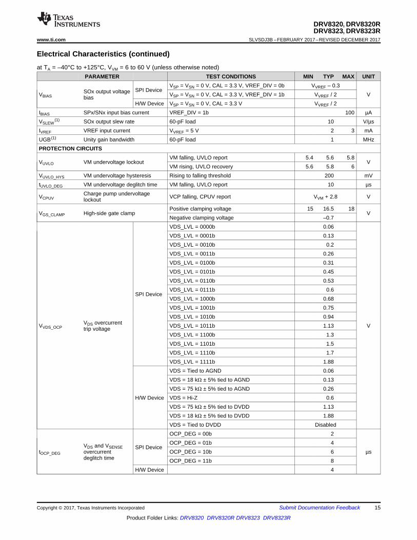
15
DRV8320, DRV8320RDRV8323, DRV8323R
www.ti.com SLVSDJ3B –FEBRUARY 2017–REVISED DECEMBER 2017
Product Folder Links: DRV8320 DRV8320R DRV8323 DRV8323R
Submit Documentation FeedbackCopyright © 2017, Texas Instruments Incorporated
Electrical Characteristics (continued)at TA = –40°C to +125°C, VVM = 6 to 60 V (unless otherwise noted)
PARAMETER TEST CONDITIONS MIN TYP MAX UNIT
VBIASSOx output voltagebias
SPI DeviceVSP = VSN = 0 V, CAL = 3.3 V, VREF_DIV = 0b VVREF – 0.3
VVSP = VSN = 0 V, CAL = 3.3 V, VREF_DIV = 1b VVREF / 2H/W Device VSP = VSN = 0 V, CAL = 3.3 V VVREF / 2
IBIAS SPx/SNx input bias current VREF_DIV = 1b 100 µAVSLEW
(1) SOx output slew rate 60-pF load 10 V/µsIVREF VREF input current VVREF = 5 V 2 3 mAUGB (1) Unity gain bandwidth 60-pF load 1 MHzPROTECTION CIRCUITS
VUVLO VM undervoltage lockoutVM falling, UVLO report 5.4 5.6 5.8
VVM rising, UVLO recovery 5.6 5.8 6
VUVLO_HYS VM undervoltage hysteresis Rising to falling threshold 200 mVtUVLO_DEG VM undervoltage deglitch time VM falling, UVLO report 10 µs
VCPUVCharge pump undervoltagelockout VCP falling, CPUV report VVM + 2.8 V
VGS_CLAMP High-side gate clampPositive clamping voltage 15 16.5 18
VNegative clamping voltage –0.7
VVDS_OCPVDS overcurrenttrip voltage
SPI Device
VDS_LVL = 0000b 0.06
V
VDS_LVL = 0001b 0.13VDS_LVL = 0010b 0.2VDS_LVL = 0011b 0.26VDS_LVL = 0100b 0.31VDS_LVL = 0101b 0.45VDS_LVL = 0110b 0.53VDS_LVL = 0111b 0.6VDS_LVL = 1000b 0.68VDS_LVL = 1001b 0.75VDS_LVL = 1010b 0.94VDS_LVL = 1011b 1.13VDS_LVL = 1100b 1.3VDS_LVL = 1101b 1.5VDS_LVL = 1110b 1.7VDS_LVL = 1111b 1.88
H/W Device
VDS = Tied to AGND 0.06VDS = 18 kΩ ± 5% tied to AGND 0.13VDS = 75 kΩ ± 5% tied to AGND 0.26VDS = Hi-Z 0.6VDS = 75 kΩ ± 5% tied to DVDD 1.13VDS = 18 kΩ ± 5% tied to DVDD 1.88VDS = Tied to DVDD Disabled
tOCP_DEG
VDS and VSENSEovercurrentdeglitch time
SPI Device
OCP_DEG = 00b 2
µsOCP_DEG = 01b 4OCP_DEG = 10b 6OCP_DEG = 11b 8
H/W Device 4
16
DRV8320, DRV8320RDRV8323, DRV8323RSLVSDJ3B –FEBRUARY 2017–REVISED DECEMBER 2017 www.ti.com
Product Folder Links: DRV8320 DRV8320R DRV8323 DRV8323R
Submit Documentation Feedback Copyright © 2017, Texas Instruments Incorporated
Electrical Characteristics (continued)at TA = –40°C to +125°C, VVM = 6 to 60 V (unless otherwise noted)
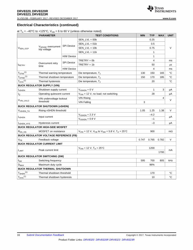
PARAMETER TEST CONDITIONS MIN TYP MAX UNIT
VSEN_OCPVSENSE overcurrenttrip voltage
SPI Device
SEN_LVL = 00b 0.25
VSEN_LVL = 01b 0.5SEN_LVL = 10b 0.75SEN_LVL = 11b 1
H/W Device 1
tRETRYOvercurrent retrytime
SPI DeviceTRETRY = 0b 4 msTRETRY = 1b 50 μs
H/W Device 4 msTOTW
(1) Thermal warning temperature Die temperature, TJ 130 150 165 °CTOTSD
(1) Thermal shutdown temperature Die temperature, TJ 150 170 185 °CTHYS
(1) Thermal hysteresis Die temperature, TJ 20 °CBUCK REGULATOR SUPPLY (VIN)InSHDN Shutdown supply current VnSHDN = 0 V 1 3 µAIQ Operating quiescent current VVIN = 12 V, no load; not switching 28 µA
VVIN_UVLOVIN undervoltage lockoutthreshold
VIN Rising 4V
VIN Falling 3BUCK REGULATOR SHUTDOWN (nSHDN)VnSHDN_TH Rising nSHDN threshold 1.05 1.25 1.38 V
InSHDN Input currentVnSHDN = 2.3 V –4.2
µAVnSHDN = 0.9 V –1
InSHDN_HYS Hysteresis current –3 µABUCK REGULATOR HIGH-SIDE MOSFETRDS_ON MOSFET on resistance VVIN = 12 V, VCB to VSW = 5.8 V, TA = 25°C 900 mΩ
BUCK REGULATOR VOLTAGE REFERENCE (FB)VFB Feedback voltage 0.747 0.765 0.782 VBUCK REGULATOR CURRENT LIMIT
ILIMIT Peak current limitVVIN = 12 V, TA = 25°C 1200
mA1700
BUCK REGULATOR SWITCHING (SW)fSW Switching frequency 595 700 805 kHzDMAX Maximum duty cycle 96%BUCK REGULATOR THERMAL SHUTDOWNTSHDN
(1) Thermal shutdown threshold 170 °CTHYS
(1) Thermal shutdown hysteresis 10 °C
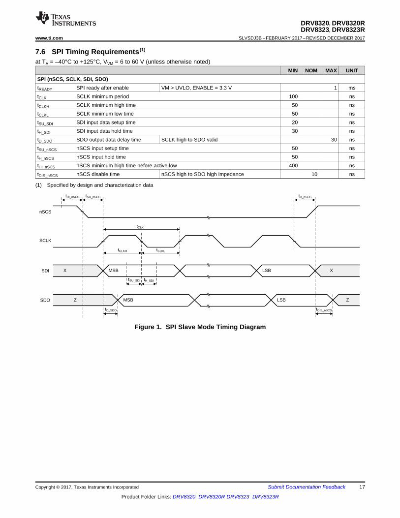
tHI_nSCS tSU_nSCS
tCLK
tCLKH tCLKL
MSB LSB
tH_SDItSU_SDI
Z ZMSB LSB
tH_nSCS
tDIS_nSCS
X X
tD_SDO
nSCS
SCLK
SDI
SDO
17
DRV8320, DRV8320RDRV8323, DRV8323R
www.ti.com SLVSDJ3B –FEBRUARY 2017–REVISED DECEMBER 2017
Product Folder Links: DRV8320 DRV8320R DRV8323 DRV8323R
Submit Documentation FeedbackCopyright © 2017, Texas Instruments Incorporated
(1) Specified by design and characterization data
7.6 SPI Timing Requirements (1)
at TA = –40°C to +125°C, VVM = 6 to 60 V (unless otherwise noted)MIN NOM MAX UNIT
SPI (nSCS, SCLK, SDI, SDO)tREADY SPI ready after enable VM > UVLO, ENABLE = 3.3 V 1 mstCLK SCLK minimum period 100 nstCLKH SCLK minimum high time 50 nstCLKL SCLK minimum low time 50 nstSU_SDI SDI input data setup time 20 nstH_SDI SDI input data hold time 30 nstD_SDO SDO output data delay time SCLK high to SDO valid 30 nstSU_nSCS nSCS input setup time 50 nstH_nSCS nSCS input hold time 50 nstHI_nSCS nSCS minimum high time before active low 400 nstDIS_nSCS nSCS disable time nSCS high to SDO high impedance 10 ns
Figure 1. SPI Slave Mode Timing Diagram
Supply Voltage (V)
DV
DD
Vol
tage
(V
)
0 10 20 30 40 50 602
2.25
2.5
2.75
3
3.25
3.5
3.75
4
D005
TA = �40qCTA = 25qCTA = 125qC
Supply Voltage (V)
DV
DD
Vol
tage
(V
)
0 10 20 30 40 50 602
2.25
2.5
2.75
3
3.25
3.5
3.75
4
D006
TA = �40qCTA = 25qCTA = 125qC
Supply Voltage (V)
Sle
ep C
urre
nt (P
A)
0 10 20 30 40 50 600
2
4
6
8
10
12
14
16
18
20
22
24
D003
TA = �40qCTA = 25qCTA = 125qC
Ambient Temperature (qC)
Sle
ep C
urre
nt (P
A)
-40 -20 0 20 40 60 80 100 120 1400
2
4
6
8
10
12
14
16
18
20
22
24
D004
VVM = 6 VVVM = 24 VVVM = 60 V
Supply Voltage (V)
Sup
ply
Cur
rent
(m
A)
0 10 20 30 40 50 600
2
4
6
8
10
12
14
16
D001
TA = �40qCTA = 25qCTA = 125qC
Ambient Temperature (°C)
Sup
ply
Cur
rent
(m
A)
-40 -20 0 20 40 60 80 100 120 1405
6
7
8
9
10
11
12
13
14
15
D002
VVM = 6 VVVM = 24 VVVM = 60 V
18
DRV8320, DRV8320RDRV8323, DRV8323RSLVSDJ3B –FEBRUARY 2017–REVISED DECEMBER 2017 www.ti.com
Product Folder Links: DRV8320 DRV8320R DRV8323 DRV8323R
Submit Documentation Feedback Copyright © 2017, Texas Instruments Incorporated
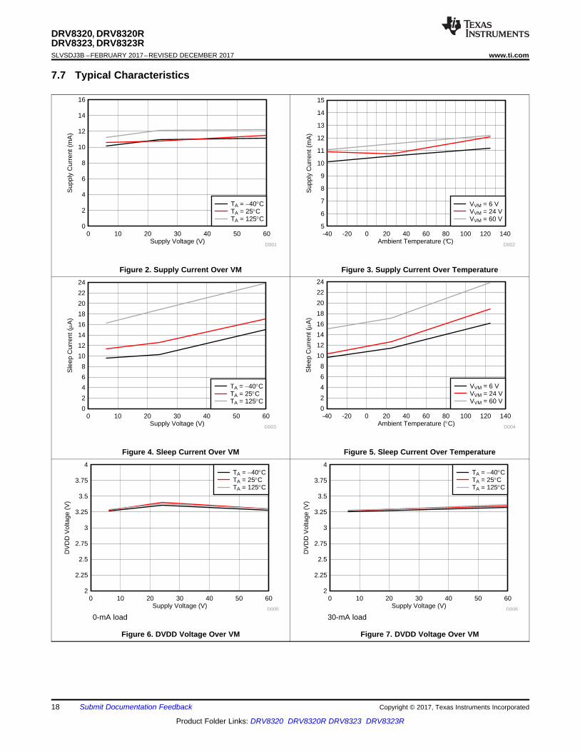
7.7 Typical Characteristics
Figure 2. Supply Current Over VM Figure 3. Supply Current Over Temperature
Figure 4. Sleep Current Over VM Figure 5. Sleep Current Over Temperature
0-mA load
Figure 6. DVDD Voltage Over VM
30-mA load
Figure 7. DVDD Voltage Over VM
Load Current (mA)
VC
P V
olta
ge (
V)
0 2.5 5 7.5 10 12.5 15 17.5 20 22.5 250
2
4
6
8
10
12
D007
VVM = 6 VVVM = 8 VVVM = 10 VVVM = 13 V
Ambient Temperature (°C)
VC
P V
olta
ge (
V)
-40 -20 0 20 40 60 80 100 120 1400
2
4
6
8
10
12
14
D008
VVM = 6 VVVM = 8 VVVM = 10 VVVM = 13 V
19
DRV8320, DRV8320RDRV8323, DRV8323R
www.ti.com SLVSDJ3B –FEBRUARY 2017–REVISED DECEMBER 2017
Product Folder Links: DRV8320 DRV8320R DRV8323 DRV8323R
Submit Documentation FeedbackCopyright © 2017, Texas Instruments Incorporated
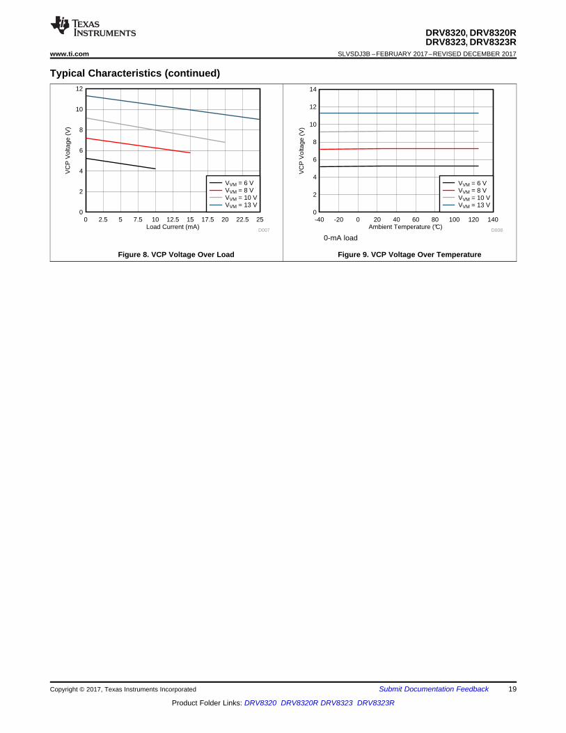
Typical Characteristics (continued)
Figure 8. VCP Voltage Over Load
0-mA load
Figure 9. VCP Voltage Over Temperature
20
DRV8320, DRV8320RDRV8323, DRV8323RSLVSDJ3B –FEBRUARY 2017–REVISED DECEMBER 2017 www.ti.com
Product Folder Links: DRV8320 DRV8320R DRV8323 DRV8323R
Submit Documentation Feedback Copyright © 2017, Texas Instruments Incorporated
8 Detailed Description
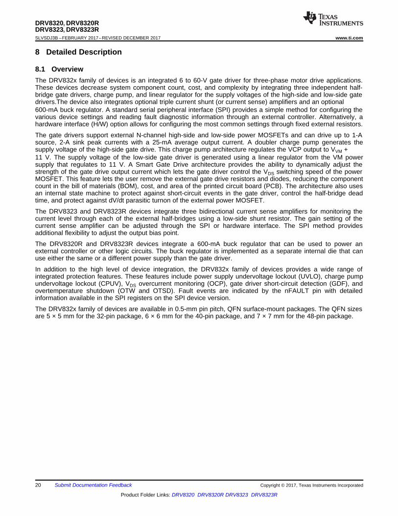
8.1 OverviewThe DRV832x family of devices is an integrated 6 to 60-V gate driver for three-phase motor drive applications.These devices decrease system component count, cost, and complexity by integrating three independent half-bridge gate drivers, charge pump, and linear regulator for the supply voltages of the high-side and low-side gatedrivers.The device also integrates optional triple current shunt (or current sense) amplifiers and an optional600-mA buck regulator. A standard serial peripheral interface (SPI) provides a simple method for configuring thevarious device settings and reading fault diagnostic information through an external controller. Alternatively, ahardware interface (H/W) option allows for configuring the most common settings through fixed external resistors.
The gate drivers support external N-channel high-side and low-side power MOSFETs and can drive up to 1-Asource, 2-A sink peak currents with a 25-mA average output current. A doubler charge pump generates thesupply voltage of the high-side gate drive. This charge pump architecture regulates the VCP output to VVM +11 V. The supply voltage of the low-side gate driver is generated using a linear regulator from the VM powersupply that regulates to 11 V. A Smart Gate Drive architecture provides the ability to dynamically adjust thestrength of the gate drive output current which lets the gate driver control the VDS switching speed of the powerMOSFET. This feature lets the user remove the external gate drive resistors and diodes, reducing the componentcount in the bill of materials (BOM), cost, and area of the printed circuit board (PCB). The architecture also usesan internal state machine to protect against short-circuit events in the gate driver, control the half-bridge deadtime, and protect against dV/dt parasitic turnon of the external power MOSFET.
The DRV8323 and DRV8323R devices integrate three bidirectional current sense amplifiers for monitoring thecurrent level through each of the external half-bridges using a low-side shunt resistor. The gain setting of thecurrent sense amplifier can be adjusted through the SPI or hardware interface. The SPI method providesadditional flexibility to adjust the output bias point.
The DRV8320R and DRV8323R devices integrate a 600-mA buck regulator that can be used to power anexternal controller or other logic circuits. The buck regulator is implemented as a separate internal die that canuse either the same or a different power supply than the gate driver.
In addition to the high level of device integration, the DRV832x family of devices provides a wide range ofintegrated protection features. These features include power supply undervoltage lockout (UVLO), charge pumpundervoltage lockout (CPUV), VDS overcurrent monitoring (OCP), gate driver short-circuit detection (GDF), andovertemperature shutdown (OTW and OTSD). Fault events are indicated by the nFAULT pin with detailedinformation available in the SPI registers on the SPI device version.
The DRV832x family of devices are available in 0.5-mm pin pitch, QFN surface-mount packages. The QFN sizesare 5 × 5 mm for the 32-pin package, 6 × 6 mm for the 40-pin package, and 7 × 7 mm for the 48-pin package.
Gate Driver
Gate Driver
Gate Driver
Fault Output
Digital Core
ControlInputs
Power
VCPCharge Pump
DVDD Linear
Regulator
VGLSLinear
Regulator
Protection
Smart Gate Drive
GHAHS
VCP
SHA
GLALS
VGLS
SLA
VM
GHBHS
VCP
SHB
GLBLS
VGLS
SLB
VM
GHCHS
VCP
SHC
GLCLS
VGLS
SLC
VM
nFAULT
VDRAINVM
0.1 �F
VM
VCP
1 �F>10 �F
CPH
CPL
DVDD
AGND
47 nF
1 �F
VGLS
INHA
INLA
INHB
INLB
INHC
ENABLE
30 mA
PGND
VDS
IDRIVE
MODE
INLC
RPU
VCC
Copyright © 2017, Texas Instruments Incorporated
21
DRV8320, DRV8320RDRV8323, DRV8323R
www.ti.com SLVSDJ3B –FEBRUARY 2017–REVISED DECEMBER 2017
Product Folder Links: DRV8320 DRV8320R DRV8323 DRV8323R
Submit Documentation FeedbackCopyright © 2017, Texas Instruments Incorporated
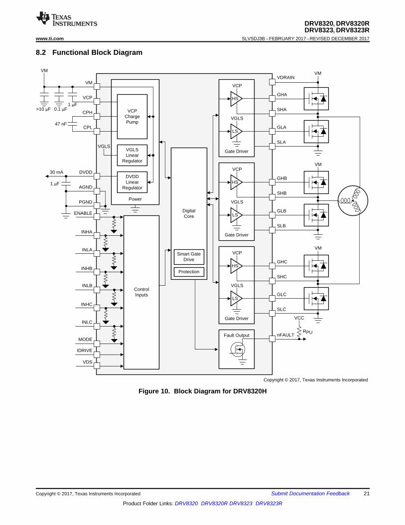
8.2 Functional Block Diagram
Figure 10. Block Diagram for DRV8320H
Gate Driver
Gate Driver
Gate Driver
Fault Output
Digital Core
ControlInputs
Power
VCPCharge Pump
DVDD Linear
Regulator
VGLSLinear
Regulator
Protection
Smart Gate Drive
SPI
GHAHS
VCP
SHA
GLALS
VGLS
SLA
VM
GHBHS
VCP
SHB
GLBLS
VGLS
SLB
VM
GHCHS
VCP
SHC
GLCLS
VGLS
SLC
VM
nFAULT
VDRAINVM
0.1 �F
VM
VCP
1 �F>10 �F
CPH
CPL47 nF
VGLS
INHA
INLA
INHB
INLB
INHC
INLC
ENABLE
SDI
DVDD
AGND1 �F
30 mA
PGND
SDO
SCLK
nSCS
RPU
VCC
RPU
VCC
Copyright © 2017, Texas Instruments Incorporated
22
DRV8320, DRV8320RDRV8323, DRV8323RSLVSDJ3B –FEBRUARY 2017–REVISED DECEMBER 2017 www.ti.com
Product Folder Links: DRV8320 DRV8320R DRV8323 DRV8323R
Submit Documentation Feedback Copyright © 2017, Texas Instruments Incorporated
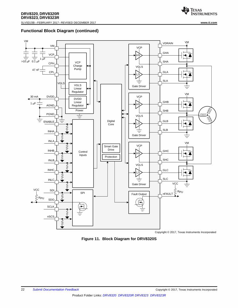
Functional Block Diagram (continued)
Figure 11. Block Diagram for DRV8320S
Gate Driver
Gate Driver
Gate Driver
Digital Core
Power
VCPCharge Pump
DVDD Linear
Regulator
VGLSLinear
Regulator
Protection
Smart Gate Drive
Buck Regulator(LMR16006X)
GHAHS
VCP
SHA
GLALS
VGLS
SLA
VM
GHBHS
VCP
SHB
GLBLS
VGLS
SLB
VM
GHCHS
VCP
SHC
GLCLS
VGLS
SLC
VM
Fault Output nFAULT
VDRAIN
ControlInputs
VM
0.1 �F
VM
VCP
1 �F>10 �F
CPH
CPL47 nF
VGLS
INHA
INLA
INHB
INLB
INHC
INLC
ENABLE
MODE
IDRIVE
VDS
VIN
nSHDN
CB
SW
BGND
CIN
VIN
FB
DVDD
AGND1 �F
30 mA
PGND
RPU
VCC
600 mA
DOUT RFB1COUT
0.1 µF
RFB2
LOUT
Copyright © 2017, Texas Instruments Incorporated
23
DRV8320, DRV8320RDRV8323, DRV8323R
www.ti.com SLVSDJ3B –FEBRUARY 2017–REVISED DECEMBER 2017
Product Folder Links: DRV8320 DRV8320R DRV8323 DRV8323R
Submit Documentation FeedbackCopyright © 2017, Texas Instruments Incorporated
Functional Block Diagram (continued)
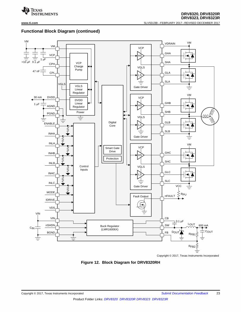
Figure 12. Block Diagram for DRV8320RH
Gate Driver
Gate Driver
Gate Driver
Fault Output
Digital Core
ControlInputs
Power
VCPCharge Pump
DVDD Linear
Regulator
VGLSLinear
Regulator
Protection
Smart Gate Drive
SPI
Buck Regulator(LMR16006X)
GHAHS
VCP
SHA
GLALS
VGLS
SLA
VM
GHBHS
VCP
SHB
GLBLS
VGLS
SLB
VM
GHCHS
VCP
SHC
GLCLS
VGLS
SLC
VM
nFAULT
VDRAINVM
0.1 �F
VM
VCP
1 �F>10 �F
CPH
CPL47 nF
VGLS
INHA
INLA
INHB
INLB
INHC
INLC
SDI
SDO
SCLK
nSCS
VIN
nSHDN
CB
SW
BGND
CIN
VIN
FB
ENABLE
DVDD
AGND1 �F
30 mA
PGND
Copyright © 2017, Texas Instruments Incorporated
0.1 µF
600 mADOUT
RFB1COUT
RFB2
LOUT
RPU
VCC
RPU
VCC
24
DRV8320, DRV8320RDRV8323, DRV8323RSLVSDJ3B –FEBRUARY 2017–REVISED DECEMBER 2017 www.ti.com
Product Folder Links: DRV8320 DRV8320R DRV8323 DRV8323R
Submit Documentation Feedback Copyright © 2017, Texas Instruments Incorporated
Functional Block Diagram (continued)
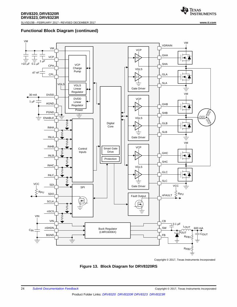
Figure 13. Block Diagram for DRV8320RS
Gate Driver
Gate Driver
Gate Driver
Fault Output
Digital Core
ControlInputs
Power
VCPCharge Pump
DVDD Linear
Regulator
VGLSLinear
Regulator
Protection
Smart Gate Drive
OutputOffsetBias
GHAHS
VCP
SHA
GLALS
VGLS
VM
GHBHS
VCP
SHB
GLBLS
VGLS
VM
GHCHS
VCP
SHC
GLCLS
VGLS
VM
nFAULT
VDRAINVM
0.1 �F
VM
VCP
1 �F>10 �F
CPH
CPL47 nF
VGLS
INHA
INLA
INHB
INLB
INHC
INLC
ENABLE
MODE
IDRIVE
VDS
AV
AV
AV
RSEN
RSEN
RSEN
SPC
SNC
SPB
SNB
SPA
SNA
SOC
SOB
SOA
VREF
0.1 �F
CAL
GAIN
DVDD
AGND1 �F
30 mA
PGND
RPU
VCC
VCC
Copyright © 2017, Texas Instruments Incorporated
25
DRV8320, DRV8320RDRV8323, DRV8323R
www.ti.com SLVSDJ3B –FEBRUARY 2017–REVISED DECEMBER 2017
Product Folder Links: DRV8320 DRV8320R DRV8323 DRV8323R
Submit Documentation FeedbackCopyright © 2017, Texas Instruments Incorporated
Functional Block Diagram (continued)
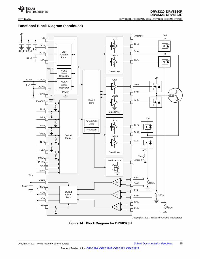
Figure 14. Block Diagram for DRV8323H
Gate Driver
Gate Driver
Gate Driver
Fault Output
Digital Core
ControlInputs
Power
OutputOffsetBias
AV
AV
AV
SPI
GHAHS
VCP
SHA
GLALS
VGLS
VM
GHBHS
VCP
SHB
GLBLS
VGLS
VM
GHCHS
VCP
SHC
GLCLS
VGLS
VM
nFAULT
VDRAINVM
0.1 �F
VM
VCP
1 �F>10 �F
CPH
CPL47 nF
VCPCharge Pump
DVDD Linear
Regulator
VGLSLinear
Regulator
VGLS
INHA
INLA
INHB
INLB
INHC
INLC
ENABLE
Protection
Smart Gate Drive
DVDD
AGND1 �F
30 mA
PGND
SOC
SOB
SOA
VREF
0.1 �F
CAL
RSEN
RSEN
SPC
SNC
SPB
SNB
SPA
SNA
RSEN
SDI
SDO
SCLK
nSCS
RPU
VCC
RPU
VCC
VCC
Copyright © 2017, Texas Instruments Incorporated
26
DRV8320, DRV8320RDRV8323, DRV8323RSLVSDJ3B –FEBRUARY 2017–REVISED DECEMBER 2017 www.ti.com
Product Folder Links: DRV8320 DRV8320R DRV8323 DRV8323R
Submit Documentation Feedback Copyright © 2017, Texas Instruments Incorporated
Functional Block Diagram (continued)
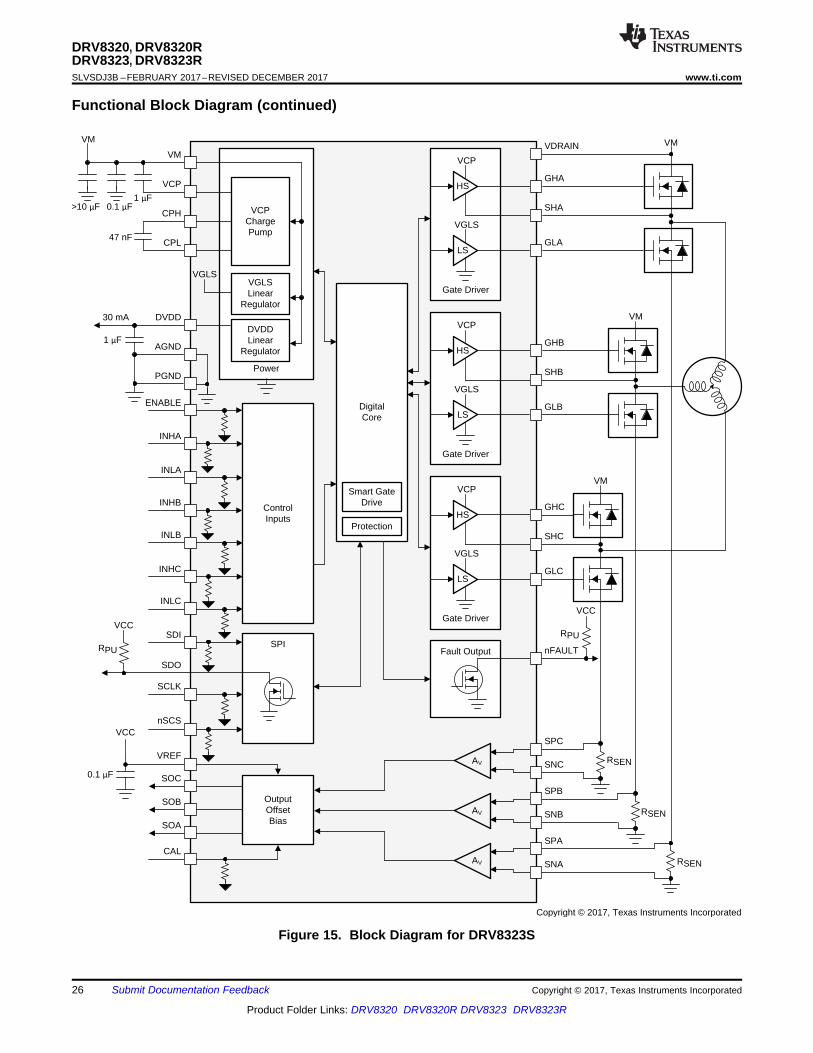
Figure 15. Block Diagram for DRV8323S
Gate Driver
Gate Driver
Gate Driver
Fault Output
Digital Core
ControlInputs
Power
VCPCharge Pump
DVDD Linear
Regulator
VGLSLinear
Regulator
Protection
Smart Gate Drive
OutputOffsetBias
Buck Regulator(LMR16006X)
GHAHS
VCP
SHA
GLALS
VGLS
VM
GHBHS
VCP
SHB
GLBLS
VGLS
VM
GHCHS
VCP
SHC
GLCLS
VGLS
VM
nFAULT
VDRAINVM
0.1 �F
VM
VCP
1 �F>10 �F
CPH
CPL
DVDD
AGND
47 nF
1 �F
VGLS
INHA
INLA
INHB
INLB
INHC
INLC
ENABLE
30 mA
MODE
IDRIVE
VDS
PGND
AV
AV
AV
RSEN
RSEN
RSEN
SPC
SNC
SPB
SNB
SPA
SNA
SOC
SOB
SOA
VREF
0.1 �F
CAL
GAIN
VIN
nSHDN
CB
SW
BGND
CIN
VIN
FB
LOUT
DGND
600 mA
DOUTRFB1 COUT
0.1 µF
RFB2
RPU
VCC
VCC
Copyright © 2017, Texas Instruments Incorporated
27
DRV8320, DRV8320RDRV8323, DRV8323R
www.ti.com SLVSDJ3B –FEBRUARY 2017–REVISED DECEMBER 2017
Product Folder Links: DRV8320 DRV8320R DRV8323 DRV8323R
Submit Documentation FeedbackCopyright © 2017, Texas Instruments Incorporated
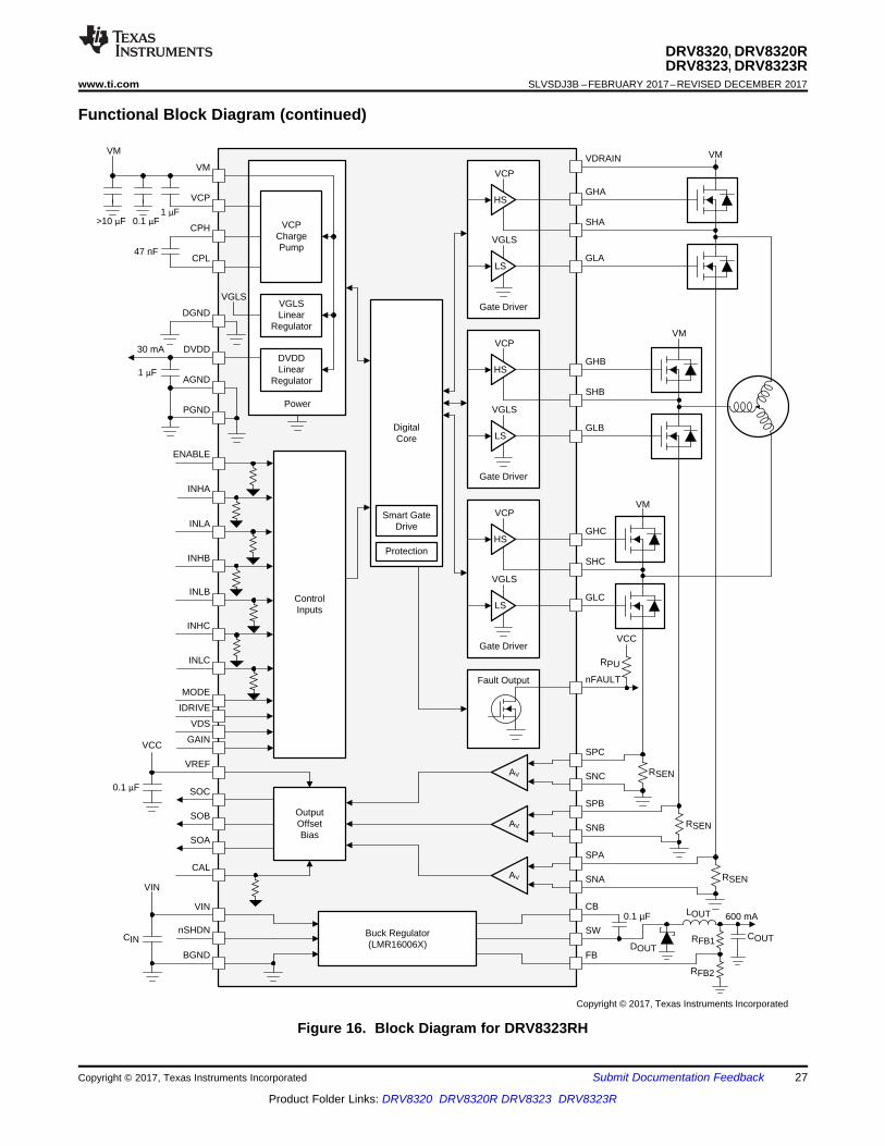
Functional Block Diagram (continued)
Figure 16. Block Diagram for DRV8323RH
Gate Driver
Gate Driver
Gate Driver
Fault Output
Digital Core
ControlInputs
Protection
Smart Gate Drive
SPI
OutputOffsetBias
Buck Regulator(LMR16006X)
Power
VCPCharge Pump
DVDD Linear
Regulator
VGLSLinear
Regulator
GHAHS
VCP
SHA
GLALS
VGLS
VM
GHBHS
VCP
SHB
GLBLS
VGLS
VM
GHCHS
VCP
SHC
GLCLS
VGLS
VM
nFAULT
VDRAIN
INHA
INLA
INHB
INLB
INHC
INLC
ENABLE
SDI
SDO
SCLK
nSCS
AV
AV
AV
RSEN
RSEN
RSEN
SPC
SNC
SPB
SNB
SPA
SNA
VIN
nSHDN
BGND
CIN
CB
SW
FB
600 mA
DOUT
LOUT
SOC
SOB
SOA
VREF
0.1 �F
CAL
VIN
VM
0.1 �F
VM
VCP1 �F
>10 �FCPH
CPL47 nF
VGLS
DGND
DVDD
AGND1 �F
30 mA
PGND
Copyright © 2017, Texas Instruments Incorporated
RPU
VCC
RFB1 COUT
0.1 µF
RFB2
RPU
VCC
VCC
28
DRV8320, DRV8320RDRV8323, DRV8323RSLVSDJ3B –FEBRUARY 2017–REVISED DECEMBER 2017 www.ti.com
Product Folder Links: DRV8320 DRV8320R DRV8323 DRV8323R
Submit Documentation Feedback Copyright © 2017, Texas Instruments Incorporated
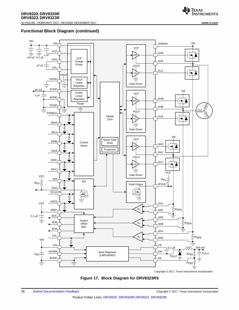
Functional Block Diagram (continued)
Figure 17. Block Diagram for DRV8323RS
29
DRV8320, DRV8320RDRV8323, DRV8323R
www.ti.com SLVSDJ3B –FEBRUARY 2017–REVISED DECEMBER 2017
Product Folder Links: DRV8320 DRV8320R DRV8323 DRV8323R
Submit Documentation FeedbackCopyright © 2017, Texas Instruments Incorporated
(1) The VCC pin is not a pin on the DRV832x family of devices, but a VCC supply voltage pullup is required for the open-drain outputs,nFAULT and SDO. These pins can also be pulled up to DVDD.
(2) The OUT pin is not a pin on the DRV8320R and DRV8323R devices, but is the regulated output voltage of the buck regulator after theoutput inductor.
8.3 Feature DescriptionTable 1 lists the recommended values of the external components for the gate driver and the buck regulator.
Table 1. DRV832x External ComponentsCOMPONENTS PIN 1 PIN 2 RECOMMENDED
GATE DRIVER AND SENSE AMPLIFIERCVM1 VM PGND X5R or X7R, 0.1-µF, VM-rated capacitorCVM2 VM PGND ≥ 10 µF, VM-rated capacitorCVCP VCP VM X5R or X7R, 16-V, 1-µF capacitorCSW CPH CPL X5R or X7R, 47-nF, VM-rated capacitor
CDVDD DVDD AGND X5R or X7R, 1-µF, 6.3-V capacitorRnFAULT VCC (1) nFAULT Pullup resistor
RSDO VCC (1) SDO Pullup resistorRIDRIVE IDRIVE AGND or DVDD DRV832x hardware interfaceRVDS VDS AGND or DVDD DRV832x hardware interface
RMODE MODE AGND or DVDD DRV832x hardware interfaceRGAIN GAIN AGND or DVDD DRV832x hardware interfaceCVREF VREF AGND or DGND X5R or X7R, 0.1-μF, VREF-rated capacitor
RASENSE SPA SNA and PGND Sense shunt resistorRBSENSE SPB SNB and PGND Sense shunt resistorRCSENSE SPC SNC and PGND Sense shunt resistor
BUCK REGULATORCVIN VIN BGND X5R or X7R, 1 to 10 µF, VM-rated capacitor
CBOOT SW CB X5R or X7R, 0.1-µF, 16-V capacitorDSW SW BGND Schottky diodeLSW SW OUT (2) Output inductorCOUT OUT (2) BGND X5R or X7R, OUT rated capacitorRFB1 OUT (2) FB
Resistor divider to set buck output voltageRFB2 FB BGND
8.3.1 Three Phase Smart Gate DriversThe DRV832x family of devices integrates three, half-bridge gate drivers, each capable of driving high-side andlow-side N-channel power MOSFETs. A doubler charge pump provides the correct gate bias voltage to the high-side MOSFET across a wide operating voltage range in addition to providing 100% support of the duty cycle. Aninternal linear regulator provides the gate bias voltage for the low-side MOSFETs. The half-bridge gate driverscan be used in combination to drive a three-phase motor or separately to drive other types of loads.
The DRV832x family of devices implements a Smart Gate Drive architecture which allows the user todynamically adjust the gate drive current without requiring external resistors to limit the gate current. Additionally,this architecture provides a variety of protection features for the external MOSFETs including automatic deadtime insertion, prevent of parasitic dV/dt gate turnon, and gate fault detection.
8.3.1.1 PWM Control ModesThe DRV832x family of devices provides four different PWM control modes to support various commutation andcontrol methods. Texas Instruments does not recommend changing the MODE pin or PWM_MODE registerduring operation of the power MOSFETs. Set all INHx and INLx pins to logic low before changing the MODE pinor PWM_MODE register.
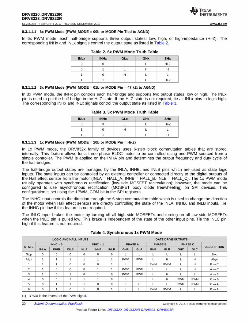
30
DRV8320, DRV8320RDRV8323, DRV8323RSLVSDJ3B –FEBRUARY 2017–REVISED DECEMBER 2017 www.ti.com
Product Folder Links: DRV8320 DRV8320R DRV8323 DRV8323R
Submit Documentation Feedback Copyright © 2017, Texas Instruments Incorporated
8.3.1.1.1 6x PWM Mode (PWM_MODE = 00b or MODE Pin Tied to AGND)
In 6x PWM mode, each half-bridge supports three output states: low, high, or high-impedance (Hi-Z). Thecorresponding INHx and INLx signals control the output state as listed in Table 2.
Table 2. 6x PWM Mode Truth TableINLx INHx GLx GHx SHx
0 0 L L Hi-Z0 1 L H H1 0 H L L1 1 L L Hi-Z
8.3.1.1.2 3x PWM Mode (PWM_MODE = 01b or MODE Pin = 47 kΩ to AGND)
In 3x PWM mode, the INHx pin controls each half-bridge and supports two output states: low or high. The INLxpin is used to put the half bridge in the Hi-Z state. If the Hi-Z state is not required, tie all INLx pins to logic high.The corresponding INHx and INLx signals control the output state as listed in Table 3.
Table 3. 3x PWM Mode Truth TableINLx INHx GLx GHx SHx
0 X L L Hi-Z1 0 H L L1 1 L H H
(1) !PWM is the inverse of the PWM signal.
8.3.1.1.3 1x PWM Mode (PWM_MODE = 10b or MODE Pin = Hi-Z)
In 1x PWM mode, the DRV832x family of devices uses 6-step block commutation tables that are storedinternally. This feature allows for a three-phase BLDC motor to be controlled using one PWM sourced from asimple controller. The PWM is applied on the INHA pin and determines the output frequency and duty cycle ofthe half-bridges.
The half-bridge output states are managed by the INLA, INHB, and INLB pins which are used as state logicinputs. The state inputs can be controlled by an external controller or connected directly to the digital outputs ofthe Hall effect sensor from the motor (INLA = HALL_A, INHB = HALL_B, INLB = HALL_C). The 1x PWM modeusually operates with synchronous rectification (low-side MOSFET recirculation); however, the mode can beconfigured to use asynchronous rectification (MOSFET body diode freewheeling) on SPI devices. Thisconfiguration is set using the 1PWM_COM bit in the SPI registers.
The INHC input controls the direction through the 6-step commutation table which is used to change the directionof the motor when Hall effect sensors are directly controlling the state of the INLA, INHB, and INLB inputs. Tiethe INHC pin low if this feature is not required.
The INLC input brakes the motor by turning off all high-side MOSFETs and turning on all low-side MOSFETswhen the INLC pin is pulled low. This brake is independent of the state of the other input pins. Tie the INLC pinhigh if this feature is not required.
Table 4. Synchronous 1x PWM ModeLOGIC AND HALL INPUTS GATE DRIVE OUTPUTS (1)
STATEINHC = 0 INHC = 1 PHASE A PHASE B PHASE C
DESCRIPTIONINLA INHB INLB INLA INHB INLB GHA GLA GHB GLB GHC GLC
Stop 0 0 0 0 0 0 L L L L L L Stop
Align 1 1 1 1 1 1 PWM !PWM L H L H Align
1 1 1 0 0 0 1 L L PWM !PWM L H B → C
2 1 0 0 0 1 1 PWM !PWM L L L H A → C
3 1 0 1 0 1 0 PWM !PWM L H L L A → B
4 0 0 1 1 1 0 L L L H PWM !PWM C → B
5 0 1 1 1 0 0 L H L L PWM !PWM C → A
6 0 1 0 1 0 1 L H PWM !PWM L L B → A
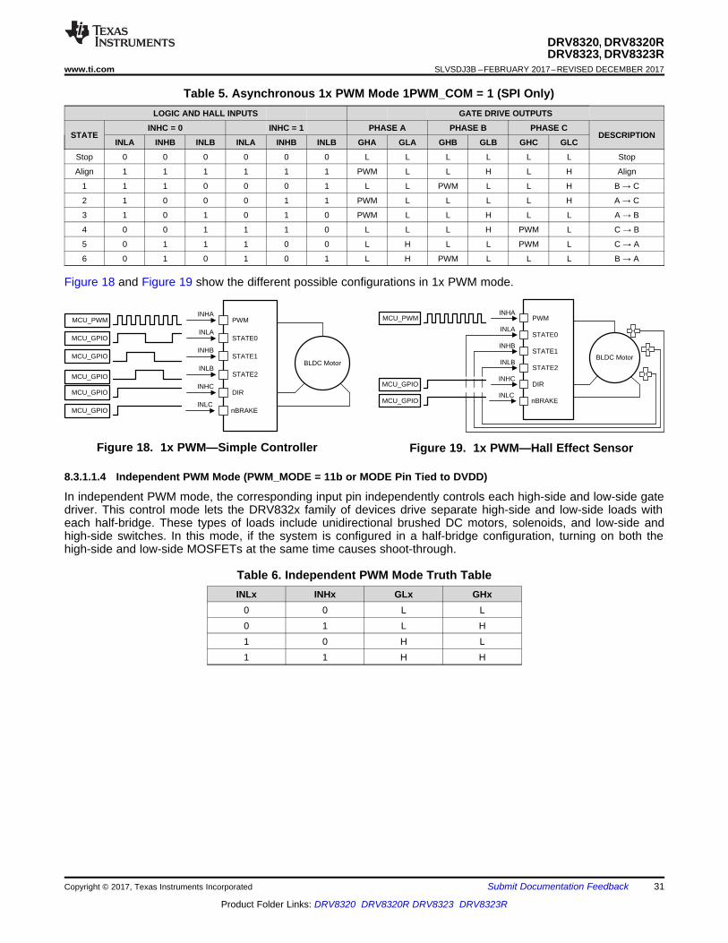
INHA
INLA
INHB
INLB
INHC
INLC
PWM
STATE0
STATE1
STATE2
DIR
nBRAKE
MCU_PWM
MCU_GPIO
MCU_GPIO
BLDC Motor
H
H
H
INHA
INLA
INHB
INLB
INHC
INLC
PWM
STATE0
STATE1
STATE2
DIR
nBRAKE
MCU_PWM
MCU_GPIO
MCU_GPIO
MCU_GPIO
MCU_GPIO
MCU_GPIO
BLDC Motor
31
DRV8320, DRV8320RDRV8323, DRV8323R
www.ti.com SLVSDJ3B –FEBRUARY 2017–REVISED DECEMBER 2017
Product Folder Links: DRV8320 DRV8320R DRV8323 DRV8323R
Submit Documentation FeedbackCopyright © 2017, Texas Instruments Incorporated
Table 5. Asynchronous 1x PWM Mode 1PWM_COM = 1 (SPI Only)LOGIC AND HALL INPUTS GATE DRIVE OUTPUTS
STATEINHC = 0 INHC = 1 PHASE A PHASE B PHASE C
DESCRIPTIONINLA INHB INLB INLA INHB INLB GHA GLA GHB GLB GHC GLC
Stop 0 0 0 0 0 0 L L L L L L Stop
Align 1 1 1 1 1 1 PWM L L H L H Align
1 1 1 0 0 0 1 L L PWM L L H B → C
2 1 0 0 0 1 1 PWM L L L L H A → C
3 1 0 1 0 1 0 PWM L L H L L A → B
4 0 0 1 1 1 0 L L L H PWM L C → B
5 0 1 1 1 0 0 L H L L PWM L C → A
6 0 1 0 1 0 1 L H PWM L L L B → A
Figure 18 and Figure 19 show the different possible configurations in 1x PWM mode.
Figure 18. 1x PWM—Simple Controller Figure 19. 1x PWM—Hall Effect Sensor
8.3.1.1.4 Independent PWM Mode (PWM_MODE = 11b or MODE Pin Tied to DVDD)
In independent PWM mode, the corresponding input pin independently controls each high-side and low-side gatedriver. This control mode lets the DRV832x family of devices drive separate high-side and low-side loads witheach half-bridge. These types of loads include unidirectional brushed DC motors, solenoids, and low-side andhigh-side switches. In this mode, if the system is configured in a half-bridge configuration, turning on both thehigh-side and low-side MOSFETs at the same time causes shoot-through.
Table 6. Independent PWM Mode Truth TableINLx INHx GLx GHx
0 0 L L0 1 L H1 0 H L1 1 H H
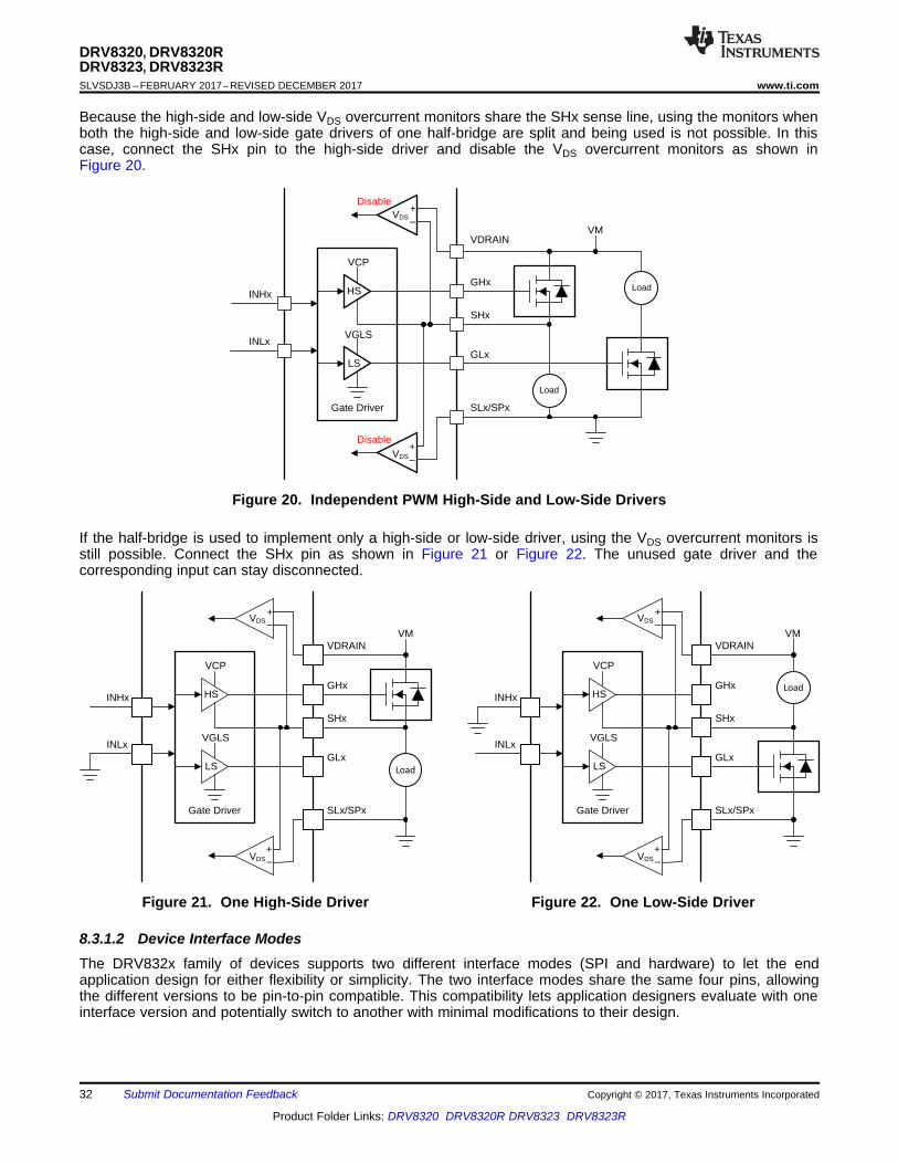
INHx
INLx
GHx
Gate Driver
HS
VCP
SHx
GLxLS
VGLS
VMVDRAIN
SLx/SPx
VDS
VDS+±
+±
Load
INHx
INLx
GHx
Gate Driver
HS
VCP
SHx
GLxLS
VGLS
VMVDRAIN
SLx/SPx
VDS
VDS+±
+±
Load
INHx
INLx
GHx
Gate Driver
HS
VCP
SHx
GLxLS
VGLS
VMVDRAIN
SLx/SPx
VDS
VDS+
+Disable
Disable
Load
Load
±
±
32
DRV8320, DRV8320RDRV8323, DRV8323RSLVSDJ3B –FEBRUARY 2017–REVISED DECEMBER 2017 www.ti.com
Product Folder Links: DRV8320 DRV8320R DRV8323 DRV8323R
Submit Documentation Feedback Copyright © 2017, Texas Instruments Incorporated
Because the high-side and low-side VDS overcurrent monitors share the SHx sense line, using the monitors whenboth the high-side and low-side gate drivers of one half-bridge are split and being used is not possible. In thiscase, connect the SHx pin to the high-side driver and disable the VDS overcurrent monitors as shown inFigure 20.
Figure 20. Independent PWM High-Side and Low-Side Drivers
If the half-bridge is used to implement only a high-side or low-side driver, using the VDS overcurrent monitors isstill possible. Connect the SHx pin as shown in Figure 21 or Figure 22. The unused gate driver and thecorresponding input can stay disconnected.
Figure 21. One High-Side Driver Figure 22. One Low-Side Driver
8.3.1.2 Device Interface ModesThe DRV832x family of devices supports two different interface modes (SPI and hardware) to let the endapplication design for either flexibility or simplicity. The two interface modes share the same four pins, allowingthe different versions to be pin-to-pin compatible. This compatibility lets application designers evaluate with oneinterface version and potentially switch to another with minimal modifications to their design.

SDI
SDO
SCLK SPIInterface
nSCS
RPU
VCC
IDRIVE
MODE
GAIN
VDS
RGAIN
DVDD
DVDD
DVDD
DVDD
DVDD
DVDD
RVDS
HardwareInterface
33
DRV8320, DRV8320RDRV8323, DRV8323R
www.ti.com SLVSDJ3B –FEBRUARY 2017–REVISED DECEMBER 2017
Product Folder Links: DRV8320 DRV8320R DRV8323 DRV8323R
Submit Documentation FeedbackCopyright © 2017, Texas Instruments Incorporated
8.3.1.2.1 Serial Peripheral Interface (SPI)
The SPI devices support a serial communication bus that lets an external controller send and receive data withthe DRV832x. This support lets the external controller configure device settings and read detailed faultinformation. The interface is a four wire interface using the SCLK, SDI, SDO, and nSCS pins which are describedas follows:• The SCLK pin is an input that accepts a clock signal to determine when data is captured and propagated on
the SDI and SDO pins.• The SDI pin is the data input.• The SDO pin is the data output. The SDO pin uses an open-drain structure and requires an external pullup
resistor.• The nSCS pin is the chip select input. A logic low signal on this pin enables SPI communication with the
DRV832x.
For more information on the SPI, see the SPI Communication section.
8.3.1.2.2 Hardware Interface
Hardware interface devices convert the four SPI pins into four resistor-configurable inputs which are GAIN,IDRIVE, MODE, and VDS. This conversion lets the application designer configure the most common devicesettings by tying the pin logic high or logic low, or with a simple pullup or pulldown resistor. This removes therequirement for an SPI bus from the external controller. General fault information can still be obtained throughthe nFAULT pin.
• The GAIN pin configures the gain of the current sense amplifier.• The IDRIVE pin configures the gate drive current strength.• The MODE pin configures the PWM control mode.• The VDS pin configures the voltage threshold of the VDS overcurrent monitors.
For more information on the hardware interface, see the Pin Diagrams section.
Figure 23. SPI Figure 24. Hardware Interface
8.3.1.3 Gate Driver Voltage SuppliesThe voltage supply for the high-side gate driver is created using a doubler charge pump that operates from theVM voltage supply input. The charge pump lets the gate driver correctly bias the high-side MOSFET gate withrespect to the source across a wide input supply voltage range. The charge pump is regulated to keep a fixedoutput voltage of VVM + 11 V and supports an average output current of 25 mA. When VVM is less than 12 V, thecharge pump operates in full doubler mode and generates VVCP = 2 × VVM – 1.5 V when unloaded. The chargepump is continuously monitored for undervoltage events to prevent under-driven MOSFET conditions. Thecharge pump requires a X5R or X7R, 1-µF, 16-V ceramic capacitor between the VM and VCP pins to act as thestorage capacitor. Additionally, a X5R or X7R, 47-nF, VM-rated ceramic capacitor is required between the CPHand CPL pins to act as the flying capacitor.
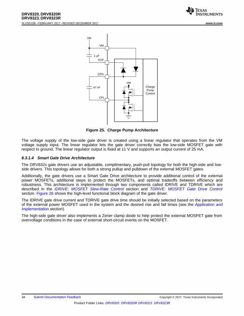
VM
VCP
1 �F
VM
CPH
Charge Pump
Control
VM
CPL
47 nF
34
DRV8320, DRV8320RDRV8323, DRV8323RSLVSDJ3B –FEBRUARY 2017–REVISED DECEMBER 2017 www.ti.com
Product Folder Links: DRV8320 DRV8320R DRV8323 DRV8323R
Submit Documentation Feedback Copyright © 2017, Texas Instruments Incorporated
Figure 25. Charge Pump Architecture
The voltage supply of the low-side gate driver is created using a linear regulator that operates from the VMvoltage supply input. The linear regulator lets the gate driver correctly bias the low-side MOSFET gate withrespect to ground. The linear regulator output is fixed at 11 V and supports an output current of 25 mA.
8.3.1.4 Smart Gate Drive ArchitectureThe DRV832x gate drivers use an adjustable, complimentary, push-pull topology for both the high-side and low-side drivers. This topology allows for both a strong pullup and pulldown of the external MOSFET gates.
Additionally, the gate drivers use a Smart Gate Drive architecture to provide additional control of the externalpower MOSFETs, additional steps to protect the MOSFETs, and optimal tradeoffs between efficiency androbustness. This architecture is implemented through two components called IDRIVE and TDRIVE which aredescribed in the IDRIVE: MOSFET Slew-Rate Control section and TDRIVE: MOSFET Gate Drive Controlsection. Figure 26 shows the high-level functional block diagram of the gate driver.
The IDRIVE gate drive current and TDRIVE gate drive time should be initially selected based on the parametersof the external power MOSFET used in the system and the desired rise and fall times (see the Application andImplementation section).
The high-side gate driver also implements a Zener clamp diode to help protect the external MOSFET gate fromovervoltage conditions in the case of external short-circuit events on the MOSFET.
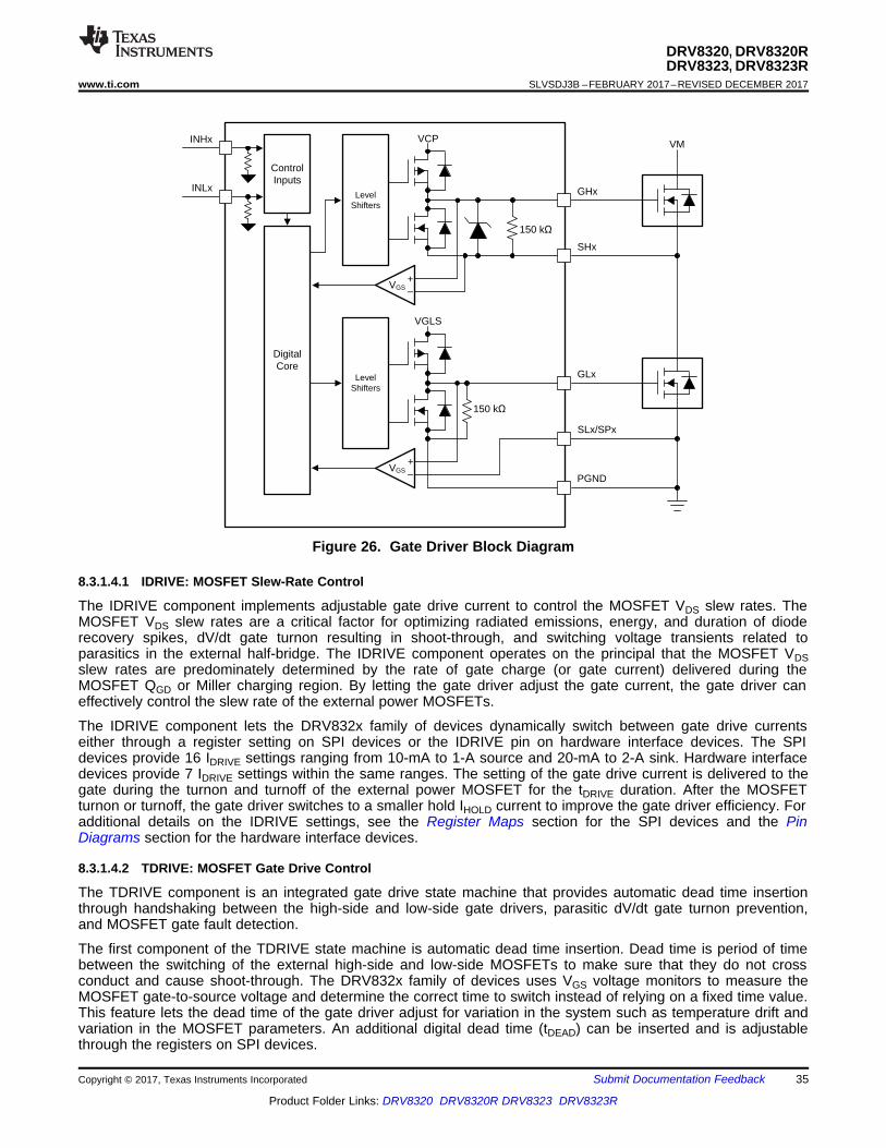
INLx
Control Inputs
INHx
Digital Core
Level Shifters
VCP
150 k
VGS+
GHx
SHx
VM
Level Shifters
VGLS
150 k
VGS+
GLx
PGND
SLx/SPx
±
±
35
DRV8320, DRV8320RDRV8323, DRV8323R
www.ti.com SLVSDJ3B –FEBRUARY 2017–REVISED DECEMBER 2017
Product Folder Links: DRV8320 DRV8320R DRV8323 DRV8323R
Submit Documentation FeedbackCopyright © 2017, Texas Instruments Incorporated
Figure 26. Gate Driver Block Diagram
8.3.1.4.1 IDRIVE: MOSFET Slew-Rate Control
The IDRIVE component implements adjustable gate drive current to control the MOSFET VDS slew rates. TheMOSFET VDS slew rates are a critical factor for optimizing radiated emissions, energy, and duration of dioderecovery spikes, dV/dt gate turnon resulting in shoot-through, and switching voltage transients related toparasitics in the external half-bridge. The IDRIVE component operates on the principal that the MOSFET VDSslew rates are predominately determined by the rate of gate charge (or gate current) delivered during theMOSFET QGD or Miller charging region. By letting the gate driver adjust the gate current, the gate driver caneffectively control the slew rate of the external power MOSFETs.
The IDRIVE component lets the DRV832x family of devices dynamically switch between gate drive currentseither through a register setting on SPI devices or the IDRIVE pin on hardware interface devices. The SPIdevices provide 16 IDRIVE settings ranging from 10-mA to 1-A source and 20-mA to 2-A sink. Hardware interfacedevices provide 7 IDRIVE settings within the same ranges. The setting of the gate drive current is delivered to thegate during the turnon and turnoff of the external power MOSFET for the tDRIVE duration. After the MOSFETturnon or turnoff, the gate driver switches to a smaller hold IHOLD current to improve the gate driver efficiency. Foradditional details on the IDRIVE settings, see the Register Maps section for the SPI devices and the PinDiagrams section for the hardware interface devices.
8.3.1.4.2 TDRIVE: MOSFET Gate Drive Control
The TDRIVE component is an integrated gate drive state machine that provides automatic dead time insertionthrough handshaking between the high-side and low-side gate drivers, parasitic dV/dt gate turnon prevention,and MOSFET gate fault detection.
The first component of the TDRIVE state machine is automatic dead time insertion. Dead time is period of timebetween the switching of the external high-side and low-side MOSFETs to make sure that they do not crossconduct and cause shoot-through. The DRV832x family of devices uses VGS voltage monitors to measure theMOSFET gate-to-source voltage and determine the correct time to switch instead of relying on a fixed time value.This feature lets the dead time of the gate driver adjust for variation in the system such as temperature drift andvariation in the MOSFET parameters. An additional digital dead time (tDEAD) can be inserted and is adjustablethrough the registers on SPI devices.
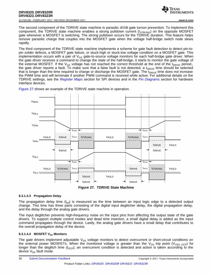
VGHx
VINHx
VINLx
IGHx
IDRIVEIHOLD
VGLx
ISTRONG
tDRIVE
tDEAD
ISTRONG
IGLx
IDRIVE IHOLD
tDEAD
tDRIVE
IDRIVE ISTRONG
tDRIVE
tDEAD
tDEAD
tDRIVE
IHOLD
IHOLD IHOLD
IHOLDIHOLD ISTRONG IHOLD
IDRIVE
IHOLD IHOLD
36
DRV8320, DRV8320RDRV8323, DRV8323RSLVSDJ3B –FEBRUARY 2017–REVISED DECEMBER 2017 www.ti.com
Product Folder Links: DRV8320 DRV8320R DRV8323 DRV8323R
Submit Documentation Feedback Copyright © 2017, Texas Instruments Incorporated
The second component of the TDRIVE state machine is parasitic dV/dt gate turnon prevention. To implement thiscomponent, the TDRIVE state machine enables a strong pulldown current (ISTRONG) on the opposite MOSFETgate whenever a MOSFET is switching. The strong pulldown occurs for the TDRIVE duration. This feature helpsremove parasitic charge that couples into the MOSFET gate when the voltage half-bridge switch node slewsrapidly.
The third component of the TDRIVE state machine implements a scheme for gate fault detection to detect pin-to-pin solder defects, a MOSFET gate failure, or stuck-high or stuck-low voltage condition on a MOSFET gate. Thisimplementation occurs with a pair of VGS gate-to-source voltage monitors for each half-bridge gate driver. Whenthe gate driver receives a command to change the state of the half-bridge, it starts to monitor the gate voltage ofthe external MOSFET. If the VGS voltage has not reached the correct threshold at the end of the tDRIVE period,,the gate driver reports a fault. To make sure that a false fault is not detected, a tDRIVE time should be selectedthat is longer than the time required to charge or discharge the MOSFET gate. The tDRIVE time does not increasethe PWM time and will terminate if another PWM command is received while active. For additional details on theTDRIVE settings, see the Register Maps section for SPI devices and in the Pin Diagrams section for hardwareinterface devices.
Figure 27 shows an example of the TDRIVE state machine in operation.
Figure 27. TDRIVE State Machine
8.3.1.4.3 Propagation Delay
The propagation delay time (tpd) is measured as the time between an input logic edge to a detected outputchange. This time has three parts consisting of the digital input deglitcher delay, the digital propagation delay,and the delay through the analog gate drivers.
The input deglitcher prevents high-frequency noise on the input pins from affecting the output state of the gatedrivers. To support multiple control modes and dead time insertion, a small digital delay is added as the inputcommand propagates through the device. Lastly, the analog gate drivers have a small delay that contributes tothe overall propagation delay of the device.
8.3.1.4.4 MOSFET VDS Monitors
The gate drivers implement adjustable VDS voltage monitors to detect overcurrent or short-circuit conditions onthe external power MOSFETs. When the monitored voltage is greater than the VDS trip point (VVDS_OCP) forlonger than the deglitch time (tOCP), an overcurrent condition is detected and action is taken according to thedevice VDS fault mode.
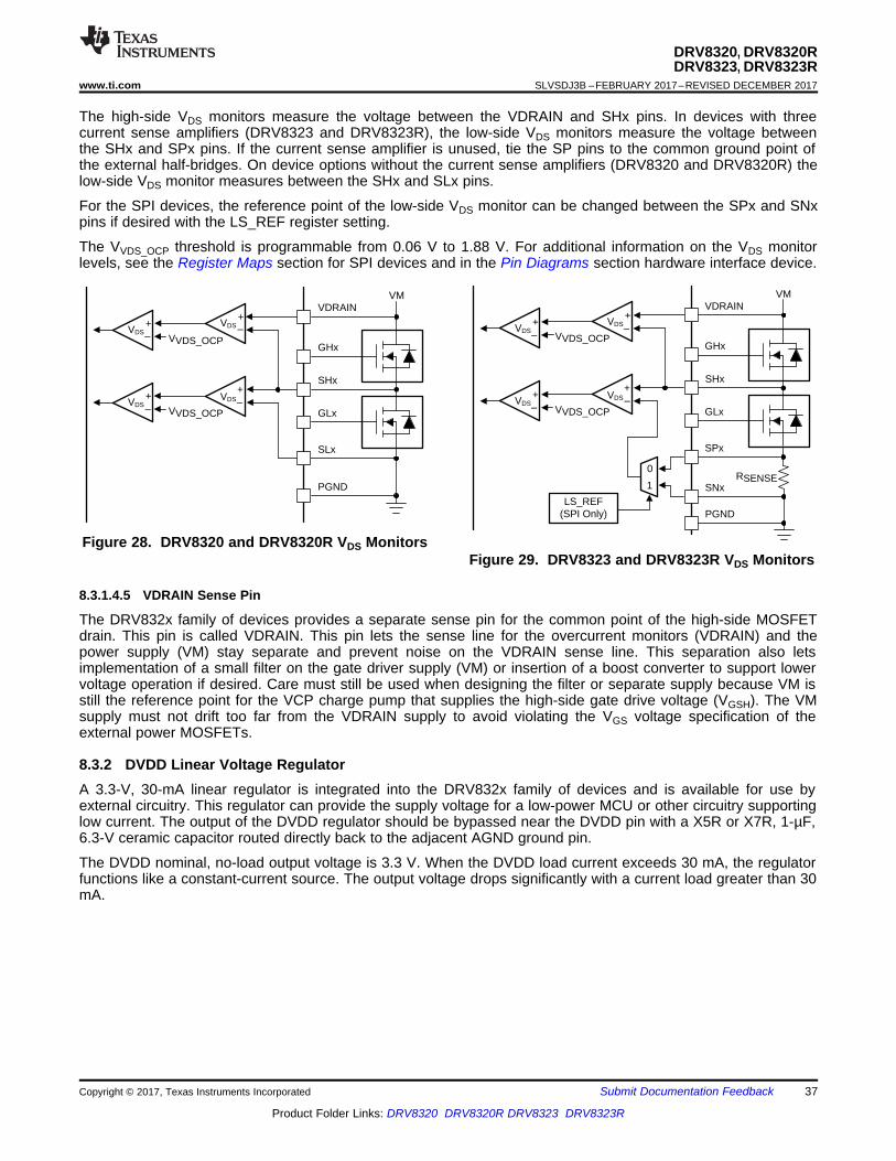
GHx
SHx
GLx
VMVDRAIN
SPx
+VDS
+VDS
+VDS
+VDS
RSENSESNx
PGNDLS_REF
(SPI Only)
0
1
VVDS_OCP
VVDS_OCP±
±
±
±
GHx
SHx
GLx
VMVDRAIN
SLx
+VDS
+VDS
+VDS
VVDS_OCP
+VDS
PGND
VVDS_OCP
±
± ±
±
37
DRV8320, DRV8320RDRV8323, DRV8323R
www.ti.com SLVSDJ3B –FEBRUARY 2017–REVISED DECEMBER 2017
Product Folder Links: DRV8320 DRV8320R DRV8323 DRV8323R
Submit Documentation FeedbackCopyright © 2017, Texas Instruments Incorporated
The high-side VDS monitors measure the voltage between the VDRAIN and SHx pins. In devices with threecurrent sense amplifiers (DRV8323 and DRV8323R), the low-side VDS monitors measure the voltage betweenthe SHx and SPx pins. If the current sense amplifier is unused, tie the SP pins to the common ground point ofthe external half-bridges. On device options without the current sense amplifiers (DRV8320 and DRV8320R) thelow-side VDS monitor measures between the SHx and SLx pins.
For the SPI devices, the reference point of the low-side VDS monitor can be changed between the SPx and SNxpins if desired with the LS_REF register setting.
The VVDS_OCP threshold is programmable from 0.06 V to 1.88 V. For additional information on the VDS monitorlevels, see the Register Maps section for SPI devices and in the Pin Diagrams section hardware interface device.
Figure 28. DRV8320 and DRV8320R VDS MonitorsFigure 29. DRV8323 and DRV8323R VDS Monitors
8.3.1.4.5 VDRAIN Sense Pin
The DRV832x family of devices provides a separate sense pin for the common point of the high-side MOSFETdrain. This pin is called VDRAIN. This pin lets the sense line for the overcurrent monitors (VDRAIN) and thepower supply (VM) stay separate and prevent noise on the VDRAIN sense line. This separation also letsimplementation of a small filter on the gate driver supply (VM) or insertion of a boost converter to support lowervoltage operation if desired. Care must still be used when designing the filter or separate supply because VM isstill the reference point for the VCP charge pump that supplies the high-side gate drive voltage (VGSH). The VMsupply must not drift too far from the VDRAIN supply to avoid violating the VGS voltage specification of theexternal power MOSFETs.
8.3.2 DVDD Linear Voltage RegulatorA 3.3-V, 30-mA linear regulator is integrated into the DRV832x family of devices and is available for use byexternal circuitry. This regulator can provide the supply voltage for a low-power MCU or other circuitry supportinglow current. The output of the DVDD regulator should be bypassed near the DVDD pin with a X5R or X7R, 1-µF,6.3-V ceramic capacitor routed directly back to the adjacent AGND ground pin.
The DVDD nominal, no-load output voltage is 3.3 V. When the DVDD load current exceeds 30 mA, the regulatorfunctions like a constant-current source. The output voltage drops significantly with a current load greater than 30mA.
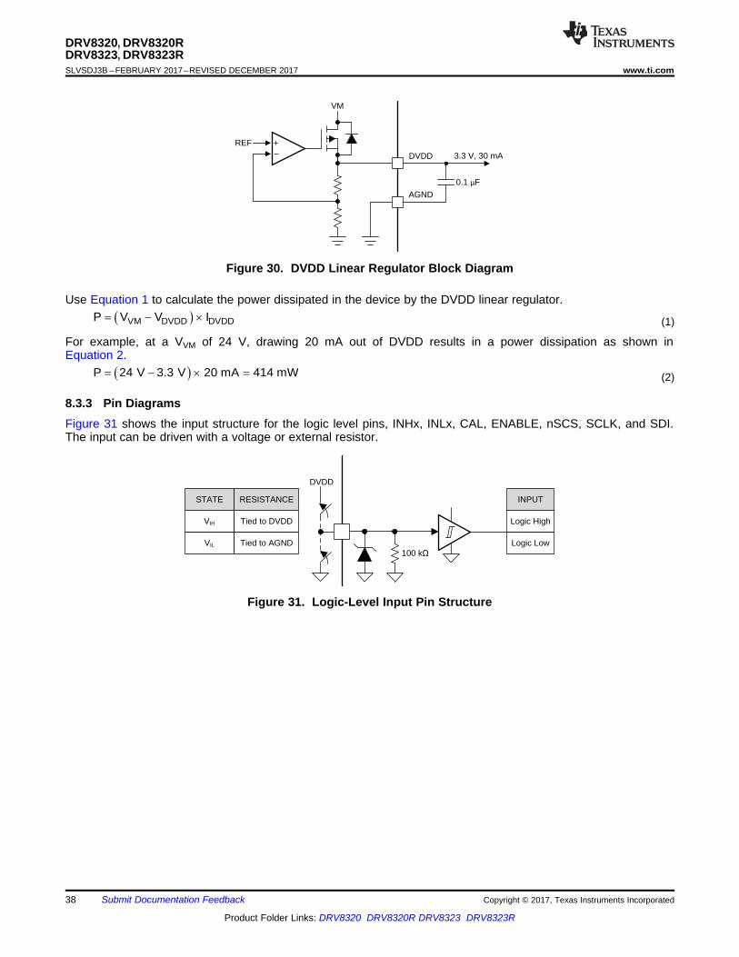
DVDD
Logic High
INPUT
VIH
STATE
Tied to DVDD
RESISTANCE
VIL Tied to AGND Logic Low100 k
� �P 24 V 3.3 V 20 mA 414 mW � u
� �VM DVDD DVDDP V V I � u
DVDD
AGND
+
0.1 �F
3.3 V, 30 mA
VM
REF±
38
DRV8320, DRV8320RDRV8323, DRV8323RSLVSDJ3B –FEBRUARY 2017–REVISED DECEMBER 2017 www.ti.com
Product Folder Links: DRV8320 DRV8320R DRV8323 DRV8323R
Submit Documentation Feedback Copyright © 2017, Texas Instruments Incorporated
Figure 30. DVDD Linear Regulator Block Diagram
Use Equation 1 to calculate the power dissipated in the device by the DVDD linear regulator.
(1)
For example, at a VVM of 24 V, drawing 20 mA out of DVDD results in a power dissipation as shown inEquation 2.
(2)
8.3.3 Pin DiagramsFigure 31 shows the input structure for the logic level pins, INHx, INLx, CAL, ENABLE, nSCS, SCLK, and SDI.The input can be driven with a voltage or external resistor.
Figure 31. Logic-Level Input Pin Structure
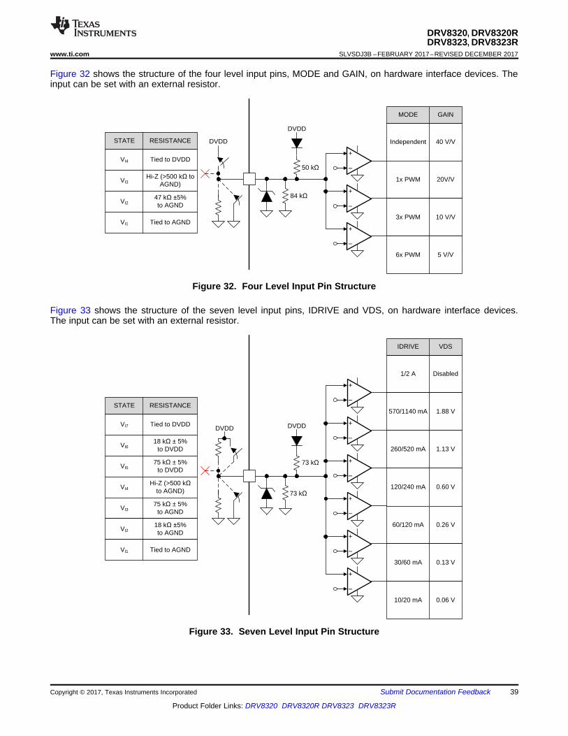
1/2 A
IDRIVE
Disabled
VDS
570/1140 mA 1.88 V
260/520 mA 1.13 V
120/240 mA 0.60 V
+
±
+
±
+
±
DVDDVI7
STATE
Tied to DVDD
RESISTANCE
VI618 k �± 5%
to DVDD
VI575 k �± 5%
to DVDD
VI4Hi-Z (>500 k��
to AGND)
DVDD
VI375 k �± 5%
to AGND
VI218 N���5% to AGND
VI1 Tied to AGND
+
±
+
±
+
±
60/120 mA 0.26 V
30/60 mA 0.13 V
10/20 mA 0.06 V
73 k
73 k
Independent
MODE
40 V/V
GAIN
1x PWM 20V/V
3x PWM 10 V/V
6x PWM 5 V/V
+
±
+
±
+
±
DVDD
VI4
STATE
Tied to DVDD
RESISTANCE
VI3Hi-Z (>500 k��WR�
AGND)
VI247 N���5% to AGND
VI1 Tied to AGND
DVDD
50 k
84 k
39
DRV8320, DRV8320RDRV8323, DRV8323R
www.ti.com SLVSDJ3B –FEBRUARY 2017–REVISED DECEMBER 2017
Product Folder Links: DRV8320 DRV8320R DRV8323 DRV8323R
Submit Documentation FeedbackCopyright © 2017, Texas Instruments Incorporated
Figure 32 shows the structure of the four level input pins, MODE and GAIN, on hardware interface devices. Theinput can be set with an external resistor.
Figure 32. Four Level Input Pin Structure
Figure 33 shows the structure of the seven level input pins, IDRIVE and VDS, on hardware interface devices.The input can be set with an external resistor.
Figure 33. Seven Level Input Pin Structure
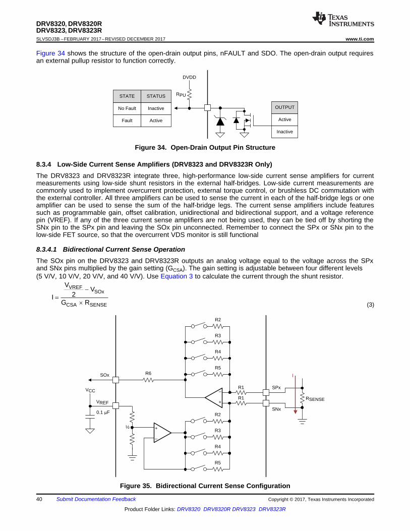
SPx
SNx
SOx
VREF
½ +
±
+
±
I
0.1 �F
R6
R4
R3
R2
R5
R1
R1
R4
R3
R2
R5
RSENSE
VCC
VREFSOx
CSA SENSE
VV
2IG R
�
u
DVDD
Active
OUTPUTNo Fault
STATE
Inactive
STATUS
Fault Active
Inactive
RPU
40
DRV8320, DRV8320RDRV8323, DRV8323RSLVSDJ3B –FEBRUARY 2017–REVISED DECEMBER 2017 www.ti.com
Product Folder Links: DRV8320 DRV8320R DRV8323 DRV8323R
Submit Documentation Feedback Copyright © 2017, Texas Instruments Incorporated
Figure 34 shows the structure of the open-drain output pins, nFAULT and SDO. The open-drain output requiresan external pullup resistor to function correctly.
Figure 34. Open-Drain Output Pin Structure
8.3.4 Low-Side Current Sense Amplifiers (DRV8323 and DRV8323R Only)The DRV8323 and DRV8323R integrate three, high-performance low-side current sense amplifiers for currentmeasurements using low-side shunt resistors in the external half-bridges. Low-side current measurements arecommonly used to implement overcurrent protection, external torque control, or brushless DC commutation withthe external controller. All three amplifiers can be used to sense the current in each of the half-bridge legs or oneamplifier can be used to sense the sum of the half-bridge legs. The current sense amplifiers include featuressuch as programmable gain, offset calibration, unidirectional and bidirectional support, and a voltage referencepin (VREF). If any of the three current sense amplifiers are not being used, they can be tied off by shorting theSNx pin to the SPx pin and leaving the SOx pin unconnected. Remember to connect the SPx or SNx pin to thelow-side FET source, so that the overcurrent VDS monitor is still functional
8.3.4.1 Bidirectional Current Sense OperationThe SOx pin on the DRV8323 and DRV8323R outputs an analog voltage equal to the voltage across the SPxand SNx pins multiplied by the gain setting (GCSA). The gain setting is adjustable between four different levels(5 V/V, 10 V/V, 20 V/V, and 40 V/V). Use Equation 3 to calculate the current through the shunt resistor.
(3)
Figure 35. Bidirectional Current Sense Configuration
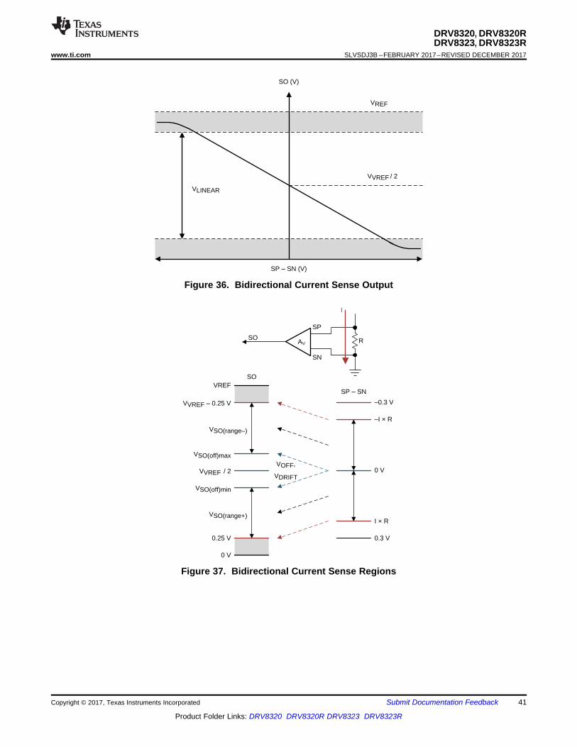
0 VVVREF / 2
VSO(off)max
VSO(off)min
VREF
VVREF ± 0.25 V
0.25 V
0 V
±I × R
I × R
SO
SP ± SN
SO
VOFF,
VDRIFT
0.3 V
±0.3 V
VSO(range±)
VSO(range+)
SP
SN
R
I
AV
SO (V)
SP ± SN (V)
VREF
VVREF / 2
VLINEAR
41
DRV8320, DRV8320RDRV8323, DRV8323R
www.ti.com SLVSDJ3B –FEBRUARY 2017–REVISED DECEMBER 2017
Product Folder Links: DRV8320 DRV8320R DRV8323 DRV8323R
Submit Documentation FeedbackCopyright © 2017, Texas Instruments Incorporated
Figure 36. Bidirectional Current Sense Output
Figure 37. Bidirectional Current Sense Regions
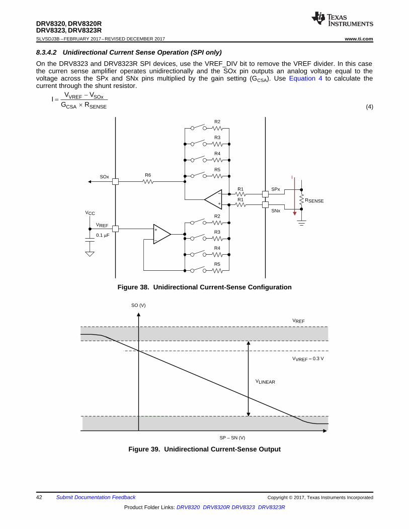
SO (V)
SP ± SN (V)
VREF
VVREF ± 0.3 V
VLINEAR
SPx
SNx
SOx
VREF+
±
+
±
I
0.1 �F
R6
R4
R3
R2
R5
R1
R1
R4
R3
R2
R5
RSENSE
VCC
VREF SOx
CSA SENSE
V VI
G R
�
u
42
DRV8320, DRV8320RDRV8323, DRV8323RSLVSDJ3B –FEBRUARY 2017–REVISED DECEMBER 2017 www.ti.com
Product Folder Links: DRV8320 DRV8320R DRV8323 DRV8323R
Submit Documentation Feedback Copyright © 2017, Texas Instruments Incorporated
8.3.4.2 Unidirectional Current Sense Operation (SPI only)On the DRV8323 and DRV8323R SPI devices, use the VREF_DIV bit to remove the VREF divider. In this casethe curren sense amplifier operates unidirectionally and the SOx pin outputs an analog voltage equal to thevoltage across the SPx and SNx pins multiplied by the gain setting (GCSA). Use Equation 4 to calculate thecurrent through the shunt resistor.
(4)
Figure 38. Unidirectional Current-Sense Configuration
Figure 39. Unidirectional Current-Sense Output
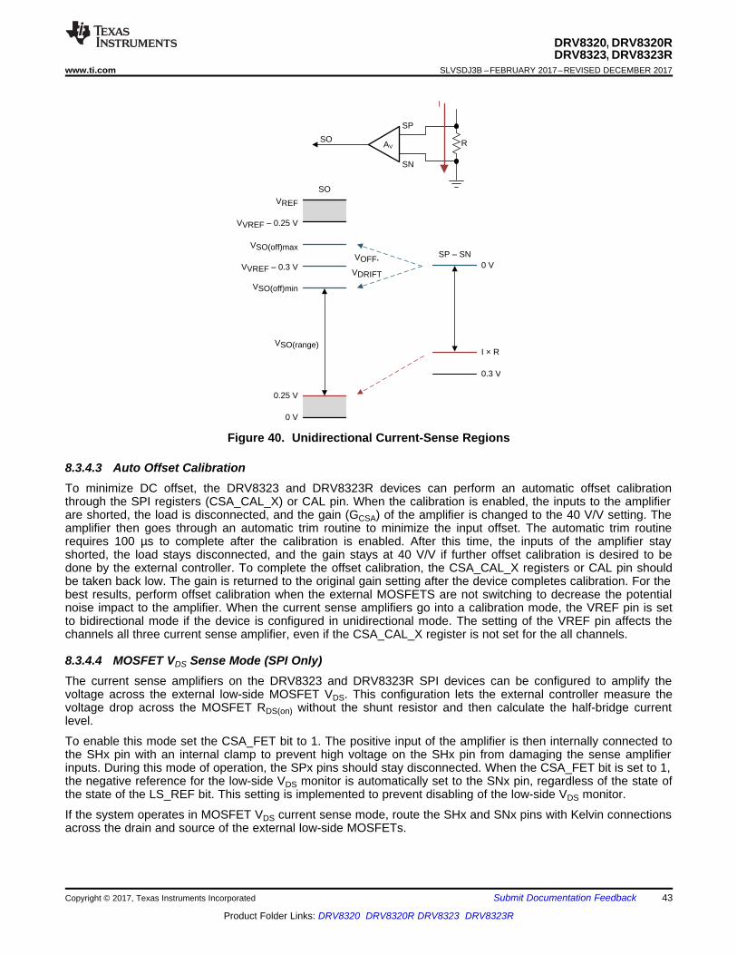
VVREF ± 0.3 V
VSO(off)max
VSO(off)min
VREF
VVREF ± 0.25 V
0.25 V
0 V
0 V
I × R
SO
SP ± SN
SO
VOFF,
VDRIFT
0.3 V
VSO(range)
SP
SN
R
I
AV
43
DRV8320, DRV8320RDRV8323, DRV8323R
www.ti.com SLVSDJ3B –FEBRUARY 2017–REVISED DECEMBER 2017
Product Folder Links: DRV8320 DRV8320R DRV8323 DRV8323R
Submit Documentation FeedbackCopyright © 2017, Texas Instruments Incorporated
Figure 40. Unidirectional Current-Sense Regions
8.3.4.3 Auto Offset CalibrationTo minimize DC offset, the DRV8323 and DRV8323R devices can perform an automatic offset calibrationthrough the SPI registers (CSA_CAL_X) or CAL pin. When the calibration is enabled, the inputs to the amplifierare shorted, the load is disconnected, and the gain (GCSA) of the amplifier is changed to the 40 V/V setting. Theamplifier then goes through an automatic trim routine to minimize the input offset. The automatic trim routinerequires 100 µs to complete after the calibration is enabled. After this time, the inputs of the amplifier stayshorted, the load stays disconnected, and the gain stays at 40 V/V if further offset calibration is desired to bedone by the external controller. To complete the offset calibration, the CSA_CAL_X registers or CAL pin shouldbe taken back low. The gain is returned to the original gain setting after the device completes calibration. For thebest results, perform offset calibration when the external MOSFETS are not switching to decrease the potentialnoise impact to the amplifier. When the current sense amplifiers go into a calibration mode, the VREF pin is setto bidirectional mode if the device is configured in unidirectional mode. The setting of the VREF pin affects thechannels all three current sense amplifier, even if the CSA_CAL_X register is not set for the all channels.
8.3.4.4 MOSFET VDS Sense Mode (SPI Only)The current sense amplifiers on the DRV8323 and DRV8323R SPI devices can be configured to amplify thevoltage across the external low-side MOSFET VDS. This configuration lets the external controller measure thevoltage drop across the MOSFET RDS(on) without the shunt resistor and then calculate the half-bridge currentlevel.
To enable this mode set the CSA_FET bit to 1. The positive input of the amplifier is then internally connected tothe SHx pin with an internal clamp to prevent high voltage on the SHx pin from damaging the sense amplifierinputs. During this mode of operation, the SPx pins should stay disconnected. When the CSA_FET bit is set to 1,the negative reference for the low-side VDS monitor is automatically set to the SNx pin, regardless of the state ofthe state of the LS_REF bit. This setting is implemented to prevent disabling of the low-side VDS monitor.
If the system operates in MOSFET VDS current sense mode, route the SHx and SNx pins with Kelvin connectionsacross the drain and source of the external low-side MOSFETs.
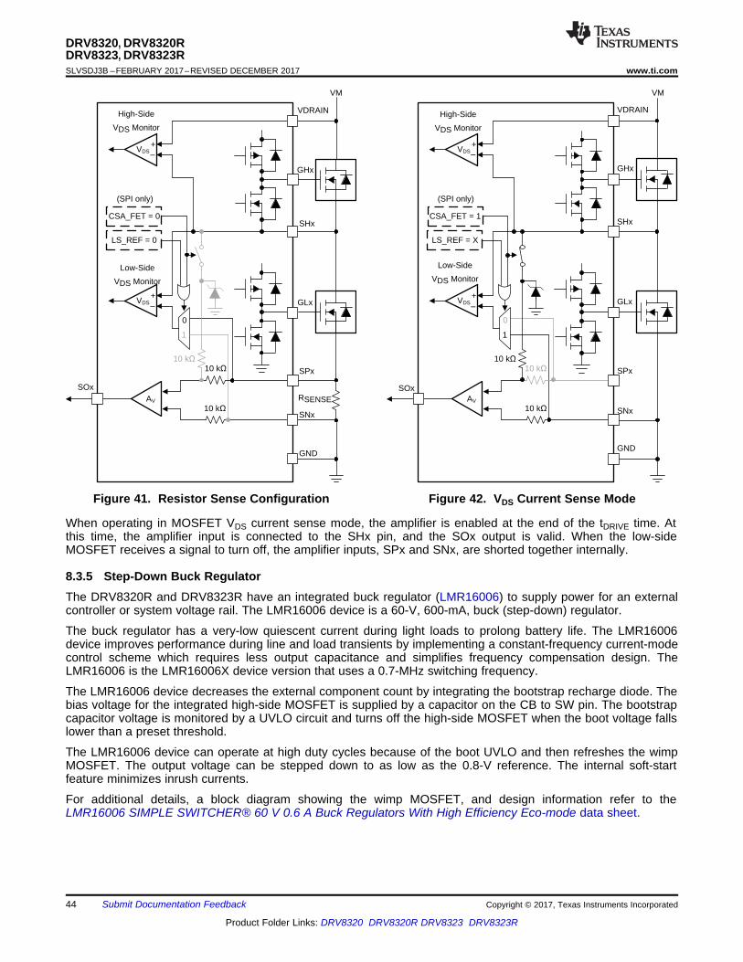
GHx
SHx
GLx
GND
VDRAIN
SNx
SPx
AV
SOx
0
1
CSA_FET = 0
LS_REF = 0
(SPI only)
VM
+VDS
Low-Side
VDS Monitor
+VDS
High-Side
VDS Monitor
10 k 10 k
10 k
±
±
RSENSE
GHx
SHx
GLx
GND
VDRAIN
SNx
SPx
AV
SOx
0
1
CSA_FET = 1
LS_REF = X
(SPI only)
VM
+VDS
Low-Side
VDS Monitor
+VDS
High-Side
VDS Monitor
10 k 10 k
10 k
±
±
44
DRV8320, DRV8320RDRV8323, DRV8323RSLVSDJ3B –FEBRUARY 2017–REVISED DECEMBER 2017 www.ti.com
Product Folder Links: DRV8320 DRV8320R DRV8323 DRV8323R
Submit Documentation Feedback Copyright © 2017, Texas Instruments Incorporated
Figure 41. Resistor Sense Configuration Figure 42. VDS Current Sense Mode
When operating in MOSFET VDS current sense mode, the amplifier is enabled at the end of the tDRIVE time. Atthis time, the amplifier input is connected to the SHx pin, and the SOx output is valid. When the low-sideMOSFET receives a signal to turn off, the amplifier inputs, SPx and SNx, are shorted together internally.
8.3.5 Step-Down Buck RegulatorThe DRV8320R and DRV8323R have an integrated buck regulator (LMR16006) to supply power for an externalcontroller or system voltage rail. The LMR16006 device is a 60-V, 600-mA, buck (step-down) regulator.
The buck regulator has a very-low quiescent current during light loads to prolong battery life. The LMR16006device improves performance during line and load transients by implementing a constant-frequency current-modecontrol scheme which requires less output capacitance and simplifies frequency compensation design. TheLMR16006 is the LMR16006X device version that uses a 0.7-MHz switching frequency.
The LMR16006 device decreases the external component count by integrating the bootstrap recharge diode. Thebias voltage for the integrated high-side MOSFET is supplied by a capacitor on the CB to SW pin. The bootstrapcapacitor voltage is monitored by a UVLO circuit and turns off the high-side MOSFET when the boot voltage fallslower than a preset threshold.
The LMR16006 device can operate at high duty cycles because of the boot UVLO and then refreshes the wimpMOSFET. The output voltage can be stepped down to as low as the 0.8-V reference. The internal soft-startfeature minimizes inrush currents.
For additional details, a block diagram showing the wimp MOSFET, and design information refer to theLMR16006 SIMPLE SWITCHER® 60 V 0.6 A Buck Regulators With High Efficiency Eco-mode data sheet.

OVR1 R2 1
0.765 V
§ ·ª º u �¨ ¸« »
¬ ¼© ¹
OR1
V 0.765 V 1R2
§ ·ª º u �¨ ¸« »
¬ ¼© ¹
45
DRV8320, DRV8320RDRV8323, DRV8323R
www.ti.com SLVSDJ3B –FEBRUARY 2017–REVISED DECEMBER 2017
Product Folder Links: DRV8320 DRV8320R DRV8323 DRV8323R
Submit Documentation FeedbackCopyright © 2017, Texas Instruments Incorporated
8.3.5.1 Fixed Frequency PWM ControlThe LMR16006 device has a fixed switching frequency and implements peak current-mode control. The outputvoltage is compared through external resistors on the FB pin to an internal voltage reference by an error amplifierwhich drives the internal COMP node. An internal oscillator initiates the turnon of the high-side power switch. Theerror amplifier output is compared to the high-side power switch current. When the power switch current reachesthe level set by the internal COMP voltage, the power switch turns off. The internal COMP node voltageincreases and decreases as the output current increases and decreases. The device implements a current limitby clamping the COMP node voltage to a maximum level.
8.3.5.2 Bootstrap Voltage (CB)The LMR16006 device has an integrated bootstrap regulator, and requires a small ceramic capacitor betweenthe CB and SW pins to provide the gate drive voltage for the high-side MOSFET. The CB capacitor is refreshedwhen the high-side MOSFET is off and the low-side diode conducts. To improve dropout, the LMR16006 deviceis designed to operate at 100% duty cycle as long as the CB to SW pin voltage is greater than 3 V. When thevoltage from the CB to SW pin drops to less than 3 V, the high-side MOSFET turns off using a UVLO circuitwhich lets the low-side diode conduct and refresh the charge on the CB capacitor. Because the supply currentsourced from the CB capacitor is low, the high-side MOSFET can stay on for more switching cycles than arerequired to refresh the capacitor. Therefore, the effective duty cycle of the switching regulator is high. Attentionmust be given in maximum duty-cycle applications with a light load. To make sure the SW pin can be pulled toground to refresh the CB capacitor, an internal circuit charges the CB capacitor when the load is light or thedevice is working in dropout condition.
8.3.5.3 Output Voltage SettingThe output voltage is set using the feedback pin (FB) and a resistor divider connected to the output as shown inFigure 51. The voltage of the feedback pin is 0.765 V, so the ratio of the feedback resistors sets the outputvoltage according to Equation 5.
(5)
Typically the starting value of R2 is from 1 kΩ to 100 kΩ. Use Equation 6 to calculate the value of R1.
(6)
8.3.5.4 Enable nSHDN and VIN Undervoltage LockoutThe nSHDN pin of the LMR16006 device is an input that is tolerant of high voltages with an internal pullup circuit.The device can be enabled even if the nSHDN pin is floating. The regulator can also be turned on using 1.23-Vor higher logic signals. If the use of a higher voltage is desired because of system or other constraints, a 100-kΩor larger value resistor is recommended between the applied voltage and the nSHDN pin to help protect thedevice. When the nSHDN pin is pulled down to 0 V, the device turns off and goes to the lowest shutdown currentmode. In shutdown mode the supply current decreases to approximately 1 µA. If the shutdown function isunused, the nSHDN pin can be tied to the VIN pin with a 100-kΩ resistor. The maximum voltage to the nSHDNpin should not exceed 60 V. The LMR16006 device has an internal UVLO circuit to shut down the output if theinput voltage falls lower than an UVLO threshold level that is internally fixed. Shutting down the output in this waymakes sure the regulator is not latched into an unknown state during low input voltage conditions. The regulatorpowers up when the input voltage exceeds the voltage level. If the UVLO voltage must be higher, use thenSHDN pin to adjust the system UVLO by using external resistors.
8.3.5.5 Current LimitThe LMR16006 device implements current-mode control which uses the internal COMP voltage to turn off thehigh-side MOSFET on a cycle-by-cycle basis. Each cycle, the switch current and internal COMP voltage arecompared. When the peak switch current intersects the COMP voltage, the high-side switch turns off. Duringovercurrent conditions that pull the output voltage low, the error amplifier responds by driving the COMP nodehigh, increasing the switch current. The error amplifier output is clamped internally causing it to function as aswitch current limit.
46
DRV8320, DRV8320RDRV8323, DRV8323RSLVSDJ3B –FEBRUARY 2017–REVISED DECEMBER 2017 www.ti.com
Product Folder Links: DRV8320 DRV8320R DRV8323 DRV8323R
Submit Documentation Feedback Copyright © 2017, Texas Instruments Incorporated
8.3.5.6 Overvoltage Transient ProtectionThe LMR16006 device incorporates an overvoltage transient protection (OVTP) circuit to minimize voltageovershoot when recovering from output fault conditions or strong unloaded transients on power supply designswith low-value output capacitance. For example, when the power supply output is overloaded, the error amplifiercompares the actual output voltage to the internal reference voltage. If the voltage of the FB pin is lower than theinternal reference voltage for a considerable time, the output of the error amplifier responds by clamping the erroramplifier output to a high voltage, therefore requesting the maximum output current. When the condition clears,the regulator output rises and the error amplifier output transitions to the steady-state duty cycle. In someapplications, the output voltage of the power supply can respond faster than the error amplifier output canrespond which can result in output overshoot. The OVTP feature minimizes the output overshoot when using alow-value output capacitor by implementing a circuit to compare the FB pin voltage to the OVTP threshold whichis 108% of the internal voltage reference. If the FB pin voltage is greater than the OVTP threshold, the high-sideMOSFET is disabled preventing current from flowing to the output and minimizing output overshoot. When theFB voltage drops lower than the OVTP threshold, the high-side MOSFET can turn on at the next clock cycle.
8.3.5.7 Thermal ShutdownThe device implements an internal thermal shutdown to help protect the device if the junction temperatureexceeds 170°C (typical). The thermal shutdown forces the device to stop switching when the junctiontemperature exceeds the thermal trip threshold. When the junction temperature decreases to less than 160°C(typical), the device reinitiates the power-up sequence.
8.3.6 Gate Driver Protective CircuitsThe DRV832x family of devices is protected against VM undervoltage, charge pump undervoltage, MOSFET VDSovercurrent, gate driver shorts, and overtemperature events.
Table 7. Fault Action and ResponseFAULT CONDITION CONFIGURATION REPORT GATE DRIVER LOGIC RECOVERY
VMundervoltage
(UVLO)VVM < VUVLO — nFAULT Hi-Z Disabled
Automatic:VVM > VUVLO
Charge pumpundervoltage
(CPUV)VVCP < VCPUV
DIS_CPUV = 0b nFAULT Hi-Z Active Automatic:VVCP > VCPUVDIS_CPUV = 1b None Active Active
VDS overcurrent(VDS_OCP) VDS > VVDS_OCP
OCP_MODE = 00b nFAULT Hi-Z ActiveLatched:
CLR_FLT, ENABLE Pulse
OCP_MODE = 01b nFAULT Hi-Z ActiveRetry:tRETRY
OCP_MODE = 10b nFAULT Active Active No action
OCP_MODE = 11b None Active Active No action
VSENSEovercurrent(SEN_OCP)
VSP > VSEN_OCP
OCP_MODE = 00b nFAULT Hi-Z ActiveLatched:
CLR_FLT, ENABLE Pulse
OCP_MODE = 01b nFAULT Hi-Z Active Retry:tRETRY
OCP_MODE = 10b nFAULT Active Active No action
OCP_MODE = 11b orDIS_SEN = 1b None Active Active No action
Gate driver fault(GDF) Gate voltage stuck > tDRIVE
DIS_GDF = 0b nFAULT Hi-Z ActiveLatched:
CLR_FLT, ENABLE Pulse
DIS_GDF = 1b None Active Active No action
Thermalwarning(OTW)
TJ > TOTW
OTW_REP = 0b None Active Active No action
OTW_REP = 1b nFAULT Active ActiveAutomatic:
TJ < TOTW – THYS
Thermalshutdown(OTSD)
TJ > TOTSD — nFAULT Hi-Z ActiveAutomatic:
TJ < TOTSD – THYS

47
DRV8320, DRV8320RDRV8323, DRV8323R
www.ti.com SLVSDJ3B –FEBRUARY 2017–REVISED DECEMBER 2017
Product Folder Links: DRV8320 DRV8320R DRV8323 DRV8323R
Submit Documentation FeedbackCopyright © 2017, Texas Instruments Incorporated
8.3.6.1 VM Supply Undervoltage Lockout (UVLO)If at any time the input supply voltage on the VM pin falls lower than the VUVLO threshold, all of the externalMOSFETs are disabled, the charge pump is disabled, and the nFAULT pin is driven low. The FAULT andVM_UVLO bits are also latched high in the registers on SPI devices. Normal operation starts again (gate driveroperation and the nFAULT pin is released) when the VM undervoltage condition clears. The VM_UVLO bit staysset until cleared through the CLR_FLT bit or an ENABLE pin reset pulse (tRST).
8.3.6.2 VCP Charge Pump Undervoltage Lockout (CPUV)If at any time the voltage on the VCP pin (charge pump) falls lower than the VCPUV threshold voltage of thecharge pump, all of the external MOSFETs are disabled and the nFAULT pin is driven low. The FAULT andCPUV bits are also latched high in the registers on SPI devices. Normal operation starts again (gate driveroperation and the nFAULT pin is released) when the VCP undervoltage condition clears. The CPUV bit stays setuntil cleared through the CLR_FLT bit or an ENABLE pin reset pulse (tRST). Setting the DIS_CPUV bit high onthe SPI devices disables this protection feature. On hardware interface devices, the CPUV protection is alwaysenabled.
8.3.6.3 MOSFET VDS Overcurrent Protection (VDS_OCP)A MOSFET overcurrent event is sensed by monitoring the VDS voltage drop across the external MOSFET RDS(on).If the voltage across an enabled MOSFET exceeds the VVDS_OCP threshold for longer than the tOCP_DEG deglitchtime, a VDS_OCP event is recognized and action is done according to the OCP_MODE bit. On hardwareinterface devices, the VVDS_OCP threshold is set with the VDS pin, the tOCP_DEG is fixed at 4 µs, and theOCP_MODE bit is configured for 4-ms automatic retry but can be disabled by tying the VDS pin to DVDD. OnSPI devices, the VVDS_OCP threshold is set through the VDS_LVL SPI register, the tOCP_DEG is set through theOCP_DEG SPI register, and the OCP_MODE bit can operate in four different modes: VDS latched shutdown, VDSautomatic retry, VDS report only, and VDS disabled.
8.3.6.3.1 VDS Latched Shutdown (OCP_MODE = 00b)
After a VDS_OCP event in this mode, all external MOSFETs are disabled and the nFAULT pin is driven low.When the external MOSFETs are disabled in this way, the driver automatically uses a lower setting for the gatedrive current instead of the programmed IDRIVE setting. This setting lets any large current that may be presentto be switched off slowly to minimize any inductive kickback caused by parasitic capacitance in the system. TheFAULT, VDS_OCP, and corresponding MOSFET OCP bits are latched high in the SPI registers. Normaloperation starts again (gate driver operation and the nFAULT pin is released) when the VDS_OCP conditionclears and a clear faults command is issued either through the CLR_FLT bit or an ENABLE reset pulse (tRST).
8.3.6.3.2 VDS Automatic Retry (OCP_MODE = 01b)
After a VDS_OCP event in this mode, all the external MOSFETs are disabled and the nFAULT pin is driven low.When the external MOSFETs are disabled in this way, the driver automatically uses a lower setting for the gatedrive current instead of the programmed IDRIVE setting. This setting lets any large current that may be presentto be switched off slowly to minimize any inductive kickback caused by parasitic capacitance in the system. TheFAULT, VDS_OCP, and corresponding MOSFET OCP bits are latched high in the SPI registers. Normaloperation starts again automatically (gate driver operation and the nFAULT pin is released) after the tRETRY timeelapses. The FAULT, VDS_OCP, and MOSFET OCP bits stay latched until the tRETRY period expires.
8.3.6.3.3 VDS Report Only (OCP_MODE = 10b)
No protective action occurs after a VDS_OCP event in this mode. The overcurrent event is reported by drivingthe nFAULT pin low and latching the FAULT, VDS_OCP, and corresponding MOSFET OCP bits high in the SPIregisters. The gate drivers continue to operate as usual. The external controller manages the overcurrentcondition by acting appropriately. The reporting clears (nFAULT pin is released) when the VDS_OCP conditionclears and a clear faults command is issued either through the CLR_FLT bit or an ENABLE reset pulse (tRST).
8.3.6.3.4 VDS Disabled (OCP_MODE = 11b)
No action occurs after a VDS_OCP event in this mode.
48
DRV8320, DRV8320RDRV8323, DRV8323RSLVSDJ3B –FEBRUARY 2017–REVISED DECEMBER 2017 www.ti.com
Product Folder Links: DRV8320 DRV8320R DRV8323 DRV8323R
Submit Documentation Feedback Copyright © 2017, Texas Instruments Incorporated
8.3.6.4 VSENSE Overcurrent Protection (SEN_OCP)Half-bridge overcurrent is also monitored by sensing the voltage drop across the external current sense resistorwith the SP pin. If at any time the voltage on the SP input of the CSA exceeds the VSEN_OCP threshold for longerthan the tOCP_DEG deglitch time, a SEN_OCP event is recognized and action is done according to theOCP_MODE bit. On hardware interface devices, the VSENSE threshold is fixed at 1 V, tOCP_DEG is fixed at 4 µs,and the OCP_MODE for VSENSE is fixed for 4-ms automatic retry. On SPI devices, the VSENSE threshold is setthrough the SEN_LVL SPI register, the tOCP_DEG is set through the OCP_DEG SPI register, and the OCP_MODEbit can operate in four different modes: VSENSE latched shutdown, VSENSE automatic retry, VSENSE report only, andVSENSE disabled.
8.3.6.4.1 VSENSE Latched Shutdown (OCP_MODE = 00b)
After a SEN_OCP event in this mode, all the external MOSFETs are disabled and the nFAULT pin is driven low.The FAULT and SEN_OCP bits are latched high in the SPI registers. Normal operation starts again (gate driveroperation and the nFAULT pin is released) when the SEN_OCP condition clears and a clear faults command isissued either through the CLR_FLT bit or an ENABLE reset pulse (tRST).
8.3.6.4.2 VSENSE Automatic Retry (OCP_MODE = 01b)
After a SEN_OCP event in this mode, all the external MOSFETs are disabled and the nFAULT pin is driven low.The FAULT, SEN_OCP, and corresponding sense OCP bits are latched high in the SPI registers. Normaloperation starts again automatically (gate driver operation and the nFAULT pin is released) after the tRETRY timeelapses. The FAULT , SEN_OCP, and sense OCP bits stay latched until the tRETRY period expires.
8.3.6.4.3 VSENSE Report Only (OCP_MODE = 10b)
No protective action occurs after a SEN_OCP event in this mode. The overcurrent event is reported by drivingthe nFAULT pin low and latching the FAULT and SEN_OCP bits high in the SPI registers. The gate driverscontinue to operate. The external controller manages the overcurrent condition by acting appropriately. Thereporting clears (nFAULT released) when the SEN_OCP condition clears and a clear faults command is issuedeither through the CLR_FLT bit or an ENABLE reset pulse (tRST).
8.3.6.4.4 VSENSE Disabled (OCP_MODE = 11b or DIS_SEN = 1b)
No action occurs after a SEN_OCP event in this mode. The SEN_OCP bit can be disabled independently of theVDS_OCP bit by using the DIS_SEN SPI register.
8.3.6.5 Gate Driver Fault (GDF)The GHx and GLx pins are monitored such that if the voltage on the external MOSFET gate does not increase ordecrease after the tDRIVE time, a gate driver fault is detected. This fault may be encountered if the GHx or GLxpins are shorted to the PGND, SHx, or VM pins. Additionally, a gate driver fault may be encountered if theselected IDRIVE setting is not sufficient to turn on the external MOSFET within the tDRIVE period. After a gate drivefault is detected, all external MOSFETs are disabled and the nFAULT pin driven low. In addition, the FAULT,GDF, and corresponding VGS bits are latched high in the SPI registers. Normal operation starts again (gatedriver operation and the nFAULT pin is released) when the gate driver fault condition clears and a clear faultscommand is issued either through the CLR_FLT bit or an ENABLE reset pulse (tRST). On SPI devices, setting theDIS_GDF bit high disables this protection feature.
Gate driver faults can indicate that the selected IDRIVE or tDRIVE settings are too low to slew the external MOSFETin the desired time. Increasing either the IDRIVE or tDRIVE setting can resolve gate driver faults in these cases.Alternatively, if a gate-to-source short occurs on the external MOSFET, a gate driver fault is reported because ofthe MOSFET gate not turning on.
8.3.6.6 Thermal Warning (OTW)If the die temperature exceeds the trip point of the thermal warning (TOTW), the OTW bit is set in the registers ofSPI devices. The device performs no additional action and continues to function. When the die temperature fallslower than the hysteresis point of the thermal warning, the OTW bit clears automatically. The OTW bit can alsobe configured to report on the nFAULT pin by setting the OTW_REP bit to 1 through the SPI registers.
49
DRV8320, DRV8320RDRV8323, DRV8323R
www.ti.com SLVSDJ3B –FEBRUARY 2017–REVISED DECEMBER 2017
Product Folder Links: DRV8320 DRV8320R DRV8323 DRV8323R
Submit Documentation FeedbackCopyright © 2017, Texas Instruments Incorporated
8.3.6.7 Thermal Shutdown (OTSD)If the die temperature exceeds the trip point of the thermal shutdown limit (TOTSD), all the external MOSFETs aredisabled, the charge pump is shut down, and the nFAULT pin is driven low. In addition, the FAULT and TSD bitsare latched high. Normal operation starts again (gate driver operation and the nFAULT pin is released) when theovertemperature condition clears. The TSD bit stays latched high indicating that a thermal event occurred until aclear fault command is issued either through the CLR_FLT bit or an ENABLE reset pulse (tRST). This protectionfeature cannot be disabled.
8.4 Device Functional Modes
8.4.1 Gate Driver Functional Modes
8.4.1.1 Sleep ModeThe ENABLE pin manages the state of the DRV832x family of devices. When the ENABLE pin is low, the devicegoes to a low-power sleep mode. In sleep mode, all gate drivers are disabled, sense amplifiers (if present) aredisabled, all external MOSFETs are disabled, the charge pump is disabled, the DVDD regulator is disabled, andthe SPI bus is disabled. The LMR16006X buck regulator (if present) is not controlled by the ENABLE pin and canbe operated independently of the gate driver. The tSLEEP time must elapse after a falling edge on the ENABLE pinbefore the device goes to sleep mode. The device comes out of sleep mode automatically if the ENABLE pin ispulled high. The tWAKE time must elapse before the device is ready for inputs.
In sleep mode and when VVM < VUVLO, all external MOSFETs are disabled. The high-side gate pins, GHx, arepulled to the SHx pin by an internal resistor and the low-side gate pins, GLx, are pulled to the PGND pin by aninternal resistor.
NOTEDuring power up and power down of the device through the ENABLE pin, the nFAULT pinis held low as the internal regulators enable or disable. After the regulators have enabledor disabled, the nFAULT pin is automatically released. The duration that the nFAULT pinis low does not exceed the tSLEEP or tWAKE time.
8.4.1.2 Operating ModeWhen the ENABLE pin is high and the VVM voltage is greater than the VUVLO voltage, the device goes tooperating mode. The tWAKE time must elapse before the device is ready for inputs. In this mode the charge pump,low-side gate regulator, DVDD regulator, and SPI bus are active
8.4.1.3 Fault Reset (CLR_FLT or ENABLE Reset Pulse)In the case of device latched faults, the DRV832x family of devices goes to a partial shutdown state to helpprotect the external power MOSFETs and system.
When the fault condition clears, the device can go to the operating state again by either setting the CLR_FLT SPIbit on SPI devices or issuing a result pulse to the ENABLE pin on either interface variant. The ENABLE resetpulse (tRST) consists of a high-to-low-to-high transition on the ENABLE pin. The low period of the sequenceshould fall with the tRST time window or else the device will start the complete shutdown sequence. The resetpulse has no effect on any of the regulators, device settings, or other functional blocks
� �D' 1 D �
O
VIN
VD
V
50
DRV8320, DRV8320RDRV8323, DRV8323RSLVSDJ3B –FEBRUARY 2017–REVISED DECEMBER 2017 www.ti.com
Product Folder Links: DRV8320 DRV8320R DRV8323 DRV8323R
Submit Documentation Feedback Copyright © 2017, Texas Instruments Incorporated
Device Functional Modes (continued)8.4.2 Buck Regulator Functional Modes
8.4.2.1 Continuous Conduction Mode (CCM)The LMR16006 integrated buck regulator steps the input voltage down to a lower output voltage. In continuousconduction mode (when the inductor current never reaches zero at CCM), the buck regulator operates in twocycles. The power switch is connected between the VIN and SW pins. During the first cycle of operation, thetransistor is closed and the diode is reverse biased. Energy is collected in the inductor and the load current issupplied by the COUT capacitor and the rising current through the inductor. During the second cycle of operation,the transistor is open and the diode is forward biased because the inductor current cannot instantaneouslychange direction. The energy stored in the inductor is transferred to the load and output capacitor. The ratio ofthese two cycles determines the output voltage. Equation 7 and Equation 8 define the approximate outputvoltage.
where• D is the duty cycle of the switch (7)
(8)
The value of D and D' is required for design calculations.
8.4.2.2 Eco-mode™ Control SchemeThe LMR16006 device operates with the Eco-mode control scheme at light-load currents to improve efficiency byreducing switching and gate drive losses. The LMR16006 device is designed so that if the output voltage iswithin regulation and the peak switch current at the end of any switching cycle is less than the sleep-currentthreshold, IINDUCTOR ≤ 80 mA, the device goes to Eco-mode. For Eco-mode operation, the LMR16006 devicesenses peak current, not average or load current, so the load current when the device goes to Eco-mode isdependent on the input voltage, the output voltage, and the value of the output inductor. When the load current islow and the output voltage is within regulation, the device goes to Eco-mode and draws only 28-µA inputquiescent current.
8.5 ProgrammingThis section applies only to the DRV832x SPI devices.
8.5.1 SPI Communication
8.5.1.1 SPIOn DRV832x SPI devices, an SPI bus is used to set device configurations, operating parameters, and read outdiagnostic information. The SPI operates in slave mode and connects to a master controller. The SPI input data(SDI) word consists of a 16-bit word, with a 5-bit command and 11 bits of data. The SPI output data (SDO) wordconsists of 11-bit register data. The first 5 bits are don’t care bits.
A valid frame must meet the following conditions:• The SCLK pin should be low when the nSCS pin transitions from high to low and from low to high.• The nSCS pin should be pulled high for at least 400 ns between words.• When the nSCS pin is pulled high, any signals at the SCLK and SDI pins are ignored and the SDO pin is
placed in the Hi-Z state.• Data is captured on the falling edge of the SCLK pin and data is propagated on the rising edge of the SCLK
pin.• The most significant bit (MSB) is shifted in and out first.• A full 16 SCLK cycles must occur for transaction to be valid.• If the data word sent to the SDI pin is less than or more than 16 bits, a frame error occurs and the data word
is ignored.• For a write command, the existing data in the register being written to is shifted out on the SDO pin following
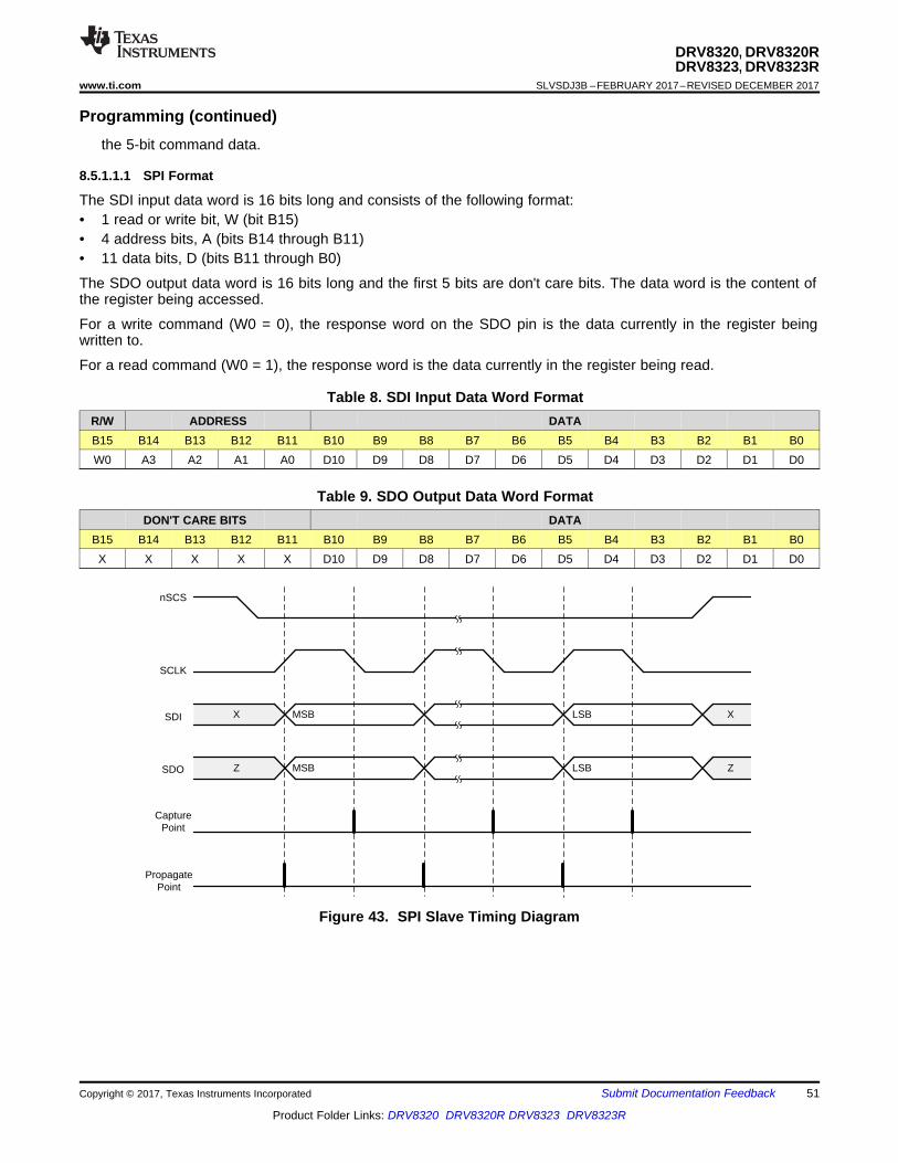
nSCS
SCLK
SDI
SDO
MSB LSB
Z ZMSB LSB
X X
CapturePoint
Propagate Point
51
DRV8320, DRV8320RDRV8323, DRV8323R
www.ti.com SLVSDJ3B –FEBRUARY 2017–REVISED DECEMBER 2017
Product Folder Links: DRV8320 DRV8320R DRV8323 DRV8323R
Submit Documentation FeedbackCopyright © 2017, Texas Instruments Incorporated
Programming (continued)the 5-bit command data.
8.5.1.1.1 SPI Format
The SDI input data word is 16 bits long and consists of the following format:• 1 read or write bit, W (bit B15)• 4 address bits, A (bits B14 through B11)• 11 data bits, D (bits B11 through B0)
The SDO output data word is 16 bits long and the first 5 bits are don't care bits. The data word is the content ofthe register being accessed.
For a write command (W0 = 0), the response word on the SDO pin is the data currently in the register beingwritten to.
For a read command (W0 = 1), the response word is the data currently in the register being read.
Table 8. SDI Input Data Word FormatR/W ADDRESS DATAB15 B14 B13 B12 B11 B10 B9 B8 B7 B6 B5 B4 B3 B2 B1 B0W0 A3 A2 A1 A0 D10 D9 D8 D7 D6 D5 D4 D3 D2 D1 D0
Table 9. SDO Output Data Word FormatDON'T CARE BITS DATA
B15 B14 B13 B12 B11 B10 B9 B8 B7 B6 B5 B4 B3 B2 B1 B0X X X X X D10 D9 D8 D7 D6 D5 D4 D3 D2 D1 D0
Figure 43. SPI Slave Timing Diagram

DRV8320, DRV8320RDRV8323, DRV8323RSLVSDJ3B –FEBRUARY 2017–REVISED DECEMBER 2017 www.ti.com
52
Product Folder Links: DRV8320 DRV8320R DRV8323 DRV8323R
Submit Documentation Feedback Copyright © 2017, Texas Instruments Incorporated
8.6 Register MapsThis section applies only to the DRV832x SPI devices.
NOTEDo not modify reserved registers or addresses not listed in the register map (Table 10). Writing to these registers may haveunintended effects. For all reserved bits, the default value is 0. To help prevent erroneous SPI writes from the master controller,set the LOCK bits to lock the SPI registers.
Table 10. DRV832xS and DRV832xRS Register MapName 10 9 8 7 6 5 4 3 2 1 0 Type Address
DRV8320S and DRV8320RSFault Status 1 FAULT VDS_OCP GDF UVLO OTSD VDS_HA VDS_LA VDS_HB VDS_LB VDS_HC VDS_LC R 0hVGS Status 2 SA_OC SB_OC SC_OC OTW CPUV VGS_HA VGS_LA VGS_HB VGS_LB VGS_HC VGS_LC R 1h
Driver Control Reserved DIS_CPUV DIS_GDF OTW_REP PWM_MODE 1PWM_COM 1PWM_DIR COAST BRAKE CLR_FLT RW 2h
Gate Drive HS LOCK IDRIVEP_HS IDRIVEN_HS RW 3hGate Drive LS CBC TDRIVE IDRIVEP_LS IDRIVEN_LS RW 4hOCP Control TRETRY DEAD_TIME OCP_MODE OCP_DEG VDS_LVL RW 5h
Reserved Reserved RW 6hReserved Reserved RW 7h
DRV8323S and DRV8323RSFault Status 1 FAULT VDS_OCP GDF UVLO OTSD VDS_HA VDS_LA VDS_HB VDS_LB VDS_HC VDS_LC R 0hVGS Status 2 SA_OC SB_OC SC_OC OTW CPUV VGS_HA VGS_LA VGS_HB VGS_LB VGS_HC VGS_LC R 1h
Driver Control Reserved DIS_CPUV DIS_GDF OTW_REP PWM_MODE 1PWM_COM 1PWM_DIR COAST BRAKE CLR_FLT RW 2h
Gate Drive HS LOCK IDRIVEP_HS IDRIVEN_HS RW 3hGate Drive LS CBC TDRIVE IDRIVEP_LS IDRIVEN_LS RW 4hOCP Control TRETRY DEAD_TIME OCP_MODE OCP_DEG VDS_LVL RW 5h
CSA Control CSA_FET VREF_DIV LS_REF CSA_GAIN DIS_SEN CSA_CAL_A
CSA_CAL_B
CSA_CAL_C SEN_LVL RW 6h
Reserved Reserved RW 7h
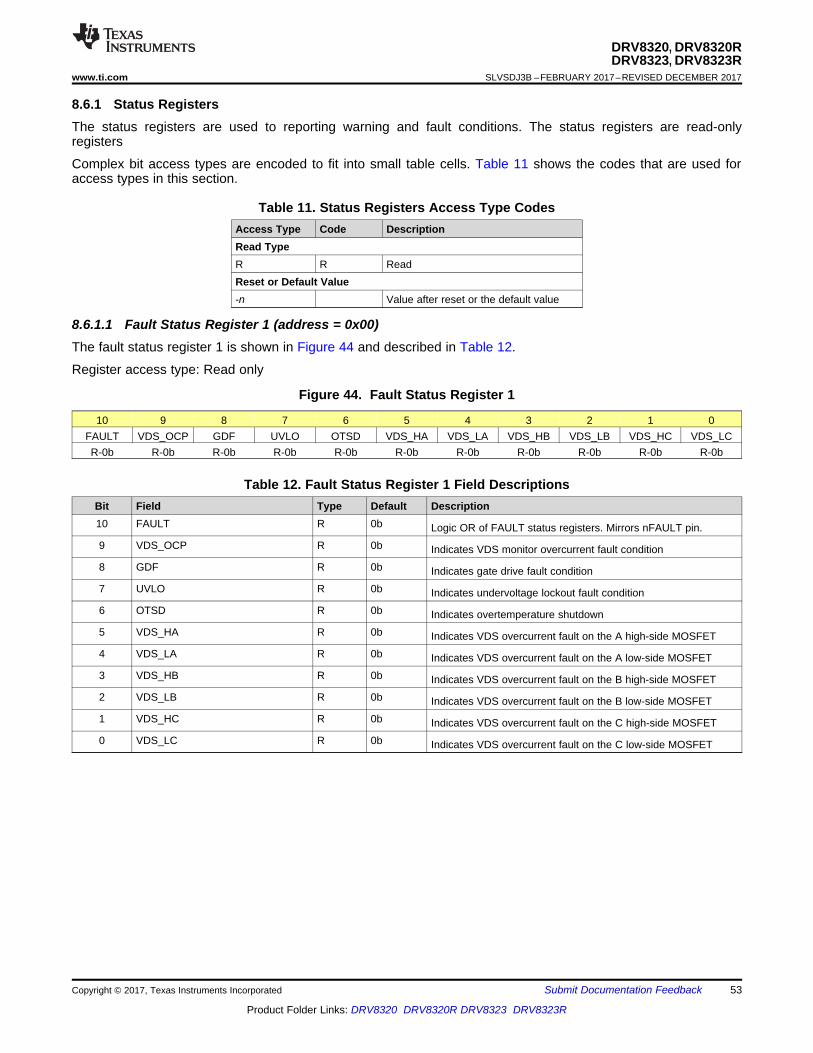
53
DRV8320, DRV8320RDRV8323, DRV8323R
www.ti.com SLVSDJ3B –FEBRUARY 2017–REVISED DECEMBER 2017
Product Folder Links: DRV8320 DRV8320R DRV8323 DRV8323R
Submit Documentation FeedbackCopyright © 2017, Texas Instruments Incorporated
8.6.1 Status RegistersThe status registers are used to reporting warning and fault conditions. The status registers are read-onlyregisters
Complex bit access types are encoded to fit into small table cells. Table 11 shows the codes that are used foraccess types in this section.
Table 11. Status Registers Access Type CodesAccess Type Code DescriptionRead TypeR R ReadReset or Default Value-n Value after reset or the default value
8.6.1.1 Fault Status Register 1 (address = 0x00)The fault status register 1 is shown in Figure 44 and described in Table 12.
Register access type: Read only
Figure 44. Fault Status Register 1
10 9 8 7 6 5 4 3 2 1 0FAULT VDS_OCP GDF UVLO OTSD VDS_HA VDS_LA VDS_HB VDS_LB VDS_HC VDS_LCR-0b R-0b R-0b R-0b R-0b R-0b R-0b R-0b R-0b R-0b R-0b
Table 12. Fault Status Register 1 Field DescriptionsBit Field Type Default Description10 FAULT R 0b Logic OR of FAULT status registers. Mirrors nFAULT pin.9 VDS_OCP R 0b Indicates VDS monitor overcurrent fault condition8 GDF R 0b Indicates gate drive fault condition7 UVLO R 0b Indicates undervoltage lockout fault condition6 OTSD R 0b Indicates overtemperature shutdown5 VDS_HA R 0b Indicates VDS overcurrent fault on the A high-side MOSFET4 VDS_LA R 0b Indicates VDS overcurrent fault on the A low-side MOSFET3 VDS_HB R 0b Indicates VDS overcurrent fault on the B high-side MOSFET2 VDS_LB R 0b Indicates VDS overcurrent fault on the B low-side MOSFET1 VDS_HC R 0b Indicates VDS overcurrent fault on the C high-side MOSFET0 VDS_LC R 0b Indicates VDS overcurrent fault on the C low-side MOSFET
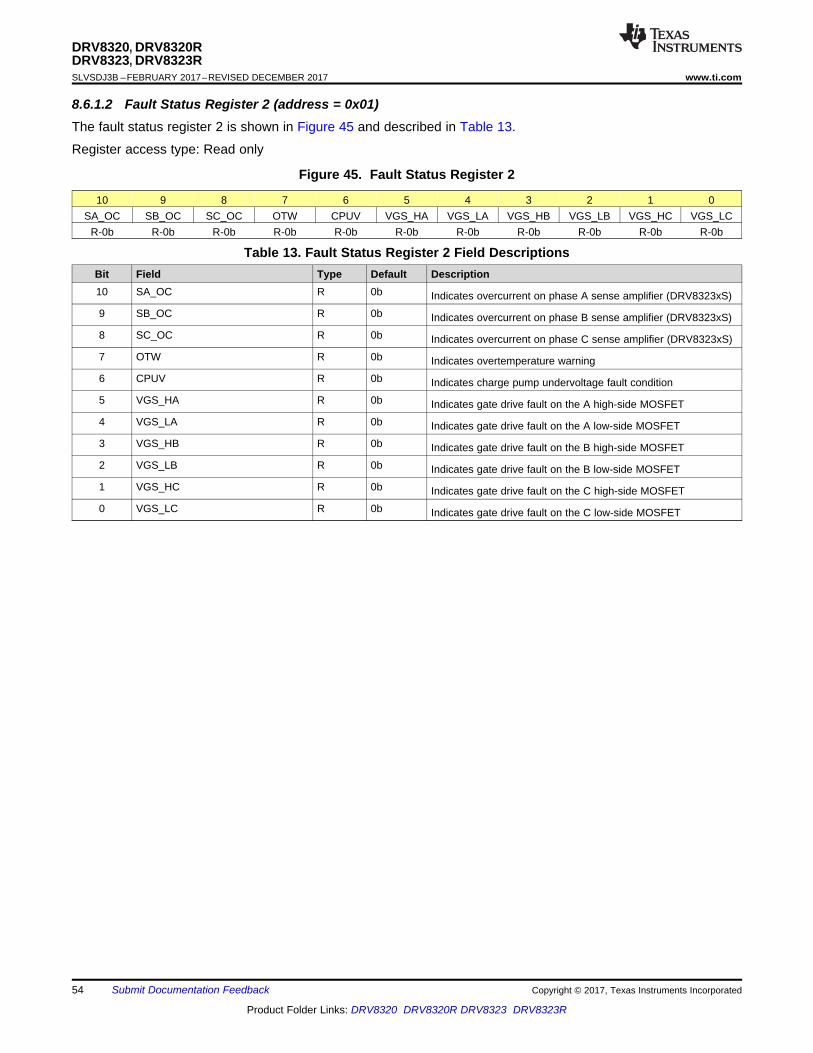
54
DRV8320, DRV8320RDRV8323, DRV8323RSLVSDJ3B –FEBRUARY 2017–REVISED DECEMBER 2017 www.ti.com
Product Folder Links: DRV8320 DRV8320R DRV8323 DRV8323R
Submit Documentation Feedback Copyright © 2017, Texas Instruments Incorporated
8.6.1.2 Fault Status Register 2 (address = 0x01)The fault status register 2 is shown in Figure 45 and described in Table 13.
Register access type: Read only
Figure 45. Fault Status Register 2
10 9 8 7 6 5 4 3 2 1 0SA_OC SB_OC SC_OC OTW CPUV VGS_HA VGS_LA VGS_HB VGS_LB VGS_HC VGS_LC
R-0b R-0b R-0b R-0b R-0b R-0b R-0b R-0b R-0b R-0b R-0b
Table 13. Fault Status Register 2 Field DescriptionsBit Field Type Default Description10 SA_OC R 0b Indicates overcurrent on phase A sense amplifier (DRV8323xS)9 SB_OC R 0b Indicates overcurrent on phase B sense amplifier (DRV8323xS)8 SC_OC R 0b Indicates overcurrent on phase C sense amplifier (DRV8323xS)7 OTW R 0b Indicates overtemperature warning6 CPUV R 0b Indicates charge pump undervoltage fault condition5 VGS_HA R 0b Indicates gate drive fault on the A high-side MOSFET4 VGS_LA R 0b Indicates gate drive fault on the A low-side MOSFET3 VGS_HB R 0b Indicates gate drive fault on the B high-side MOSFET2 VGS_LB R 0b Indicates gate drive fault on the B low-side MOSFET1 VGS_HC R 0b Indicates gate drive fault on the C high-side MOSFET0 VGS_LC R 0b Indicates gate drive fault on the C low-side MOSFET
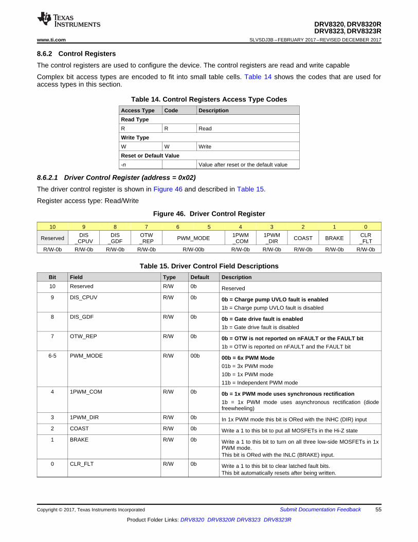
55
DRV8320, DRV8320RDRV8323, DRV8323R
www.ti.com SLVSDJ3B –FEBRUARY 2017–REVISED DECEMBER 2017
Product Folder Links: DRV8320 DRV8320R DRV8323 DRV8323R
Submit Documentation FeedbackCopyright © 2017, Texas Instruments Incorporated
8.6.2 Control RegistersThe control registers are used to configure the device. The control registers are read and write capable
Complex bit access types are encoded to fit into small table cells. Table 14 shows the codes that are used foraccess types in this section.
Table 14. Control Registers Access Type CodesAccess Type Code DescriptionRead TypeR R ReadWrite TypeW W WriteReset or Default Value-n Value after reset or the default value
8.6.2.1 Driver Control Register (address = 0x02)The driver control register is shown in Figure 46 and described in Table 15.
Register access type: Read/Write
Figure 46. Driver Control Register
10 9 8 7 6 5 4 3 2 1 0
Reserved DIS_CPUV
DIS_GDF
OTW_REP PWM_MODE 1PWM
_COM1PWM_DIR COAST BRAKE CLR
_FLTR/W-0b R/W-0b R/W-0b R/W-0b R/W-00b R/W-0b R/W-0b R/W-0b R/W-0b R/W-0b
Table 15. Driver Control Field DescriptionsBit Field Type Default Description10 Reserved R/W 0b Reserved9 DIS_CPUV R/W 0b 0b = Charge pump UVLO fault is enabled
1b = Charge pump UVLO fault is disabled8 DIS_GDF R/W 0b 0b = Gate drive fault is enabled
1b = Gate drive fault is disabled7 OTW_REP R/W 0b 0b = OTW is not reported on nFAULT or the FAULT bit
1b = OTW is reported on nFAULT and the FAULT bit6-5 PWM_MODE R/W 00b 00b = 6x PWM Mode
01b = 3x PWM mode10b = 1x PWM mode11b = Independent PWM mode
4 1PWM_COM R/W 0b 0b = 1x PWM mode uses synchronous rectification1b = 1x PWM mode uses asynchronous rectification (diodefreewheeling)
3 1PWM_DIR R/W 0b In 1x PWM mode this bit is ORed with the INHC (DIR) input2 COAST R/W 0b Write a 1 to this bit to put all MOSFETs in the Hi-Z state1 BRAKE R/W 0b Write a 1 to this bit to turn on all three low-side MOSFETs in 1x
PWM mode.This bit is ORed with the INLC (BRAKE) input.
0 CLR_FLT R/W 0b Write a 1 to this bit to clear latched fault bits.This bit automatically resets after being written.
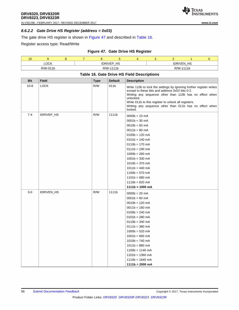
56
DRV8320, DRV8320RDRV8323, DRV8323RSLVSDJ3B –FEBRUARY 2017–REVISED DECEMBER 2017 www.ti.com
Product Folder Links: DRV8320 DRV8320R DRV8323 DRV8323R
Submit Documentation Feedback Copyright © 2017, Texas Instruments Incorporated
8.6.2.2 Gate Drive HS Register (address = 0x03)The gate drive HS register is shown in Figure 47 and described in Table 16.
Register access type: Read/Write
Figure 47. Gate Drive HS Register
10 9 8 7 6 5 4 3 2 1 0LOCK IDRIVEP_HS IDRIVEN_HS
R/W-011b R/W-1111b R/W-1111b
Table 16. Gate Drive HS Field DescriptionsBit Field Type Default Description
10-8 LOCK R/W 011b Write 110b to lock the settings by ignoring further register writesexcept to these bits and address 0x02 bits 0-2.Writing any sequence other than 110b has no effect whenunlocked.Write 011b to this register to unlock all registers.Writing any sequence other than 011b has no effect whenlocked.
7-4 IDRIVEP_HS R/W 1111b 0000b = 10 mA0001b = 30 mA0010b = 60 mA0011b = 80 mA0100b = 120 mA0101b = 140 mA0110b = 170 mA0111b = 190 mA1000b = 260 mA1001b = 330 mA1010b = 370 mA1011b = 440 mA1100b = 570 mA1101b = 680 mA1110b = 820 mA1111b = 1000 mA
3-0 IDRIVEN_HS R/W 1111b 0000b = 20 mA0001b = 60 mA0010b = 120 mA0011b = 160 mA0100b = 240 mA0101b = 280 mA0110b = 340 mA0111b = 380 mA1000b = 520 mA1001b = 660 mA1010b = 740 mA1011b = 880 mA1100b = 1140 mA1101b = 1360 mA1110b = 1640 mA1111b = 2000 mA
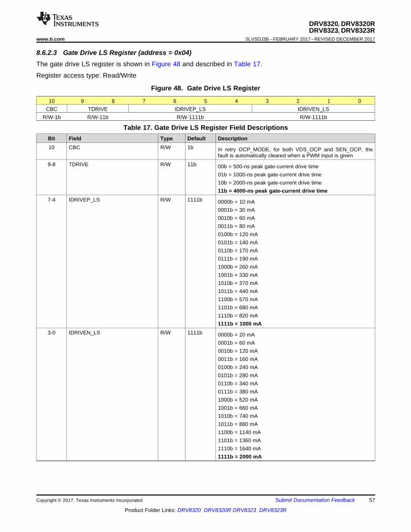
57
DRV8320, DRV8320RDRV8323, DRV8323R
www.ti.com SLVSDJ3B –FEBRUARY 2017–REVISED DECEMBER 2017
Product Folder Links: DRV8320 DRV8320R DRV8323 DRV8323R
Submit Documentation FeedbackCopyright © 2017, Texas Instruments Incorporated
8.6.2.3 Gate Drive LS Register (address = 0x04)The gate drive LS register is shown in Figure 48 and described in Table 17.
Register access type: Read/Write
Figure 48. Gate Drive LS Register
10 9 8 7 6 5 4 3 2 1 0CBC TDRIVE IDRIVEP_LS IDRIVEN_LS
R/W-1b R/W-11b R/W-1111b R/W-1111b
Table 17. Gate Drive LS Register Field DescriptionsBit Field Type Default Description10 CBC R/W 1b In retry OCP_MODE, for both VDS_OCP and SEN_OCP, the
fault is automatically cleared when a PWM input is given9-8 TDRIVE R/W 11b 00b = 500-ns peak gate-current drive time
01b = 1000-ns peak gate-current drive time10b = 2000-ns peak gate-current drive time11b = 4000-ns peak gate-current drive time
7-4 IDRIVEP_LS R/W 1111b 0000b = 10 mA0001b = 30 mA0010b = 60 mA0011b = 80 mA0100b = 120 mA0101b = 140 mA0110b = 170 mA0111b = 190 mA1000b = 260 mA1001b = 330 mA1010b = 370 mA1011b = 440 mA1100b = 570 mA1101b = 680 mA1110b = 820 mA1111b = 1000 mA
3-0 IDRIVEN_LS R/W 1111b 0000b = 20 mA0001b = 60 mA0010b = 120 mA0011b = 160 mA0100b = 240 mA0101b = 280 mA0110b = 340 mA0111b = 380 mA1000b = 520 mA1001b = 660 mA1010b = 740 mA1011b = 880 mA1100b = 1140 mA1101b = 1360 mA1110b = 1640 mA1111b = 2000 mA
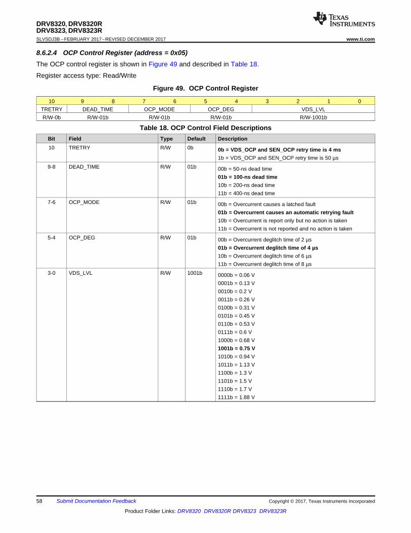
58
DRV8320, DRV8320RDRV8323, DRV8323RSLVSDJ3B –FEBRUARY 2017–REVISED DECEMBER 2017 www.ti.com
Product Folder Links: DRV8320 DRV8320R DRV8323 DRV8323R
Submit Documentation Feedback Copyright © 2017, Texas Instruments Incorporated
8.6.2.4 OCP Control Register (address = 0x05)The OCP control register is shown in Figure 49 and described in Table 18.
Register access type: Read/Write
Figure 49. OCP Control Register
10 9 8 7 6 5 4 3 2 1 0TRETRY DEAD_TIME OCP_MODE OCP_DEG VDS_LVLR/W-0b R/W-01b R/W-01b R/W-01b R/W-1001b
Table 18. OCP Control Field DescriptionsBit Field Type Default Description10 TRETRY R/W 0b 0b = VDS_OCP and SEN_OCP retry time is 4 ms
1b = VDS_OCP and SEN_OCP retry time is 50 µs9-8 DEAD_TIME R/W 01b 00b = 50-ns dead time
01b = 100-ns dead time10b = 200-ns dead time11b = 400-ns dead time
7-6 OCP_MODE R/W 01b 00b = Overcurrent causes a latched fault01b = Overcurrent causes an automatic retrying fault10b = Overcurrent is report only but no action is taken11b = Overcurrent is not reported and no action is taken
5-4 OCP_DEG R/W 01b 00b = Overcurrent deglitch time of 2 µs01b = Overcurrent deglitch time of 4 µs10b = Overcurrent deglitch time of 6 µs11b = Overcurrent deglitch time of 8 µs
3-0 VDS_LVL R/W 1001b 0000b = 0.06 V0001b = 0.13 V0010b = 0.2 V0011b = 0.26 V0100b = 0.31 V0101b = 0.45 V0110b = 0.53 V0111b = 0.6 V1000b = 0.68 V1001b = 0.75 V1010b = 0.94 V1011b = 1.13 V1100b = 1.3 V1101b = 1.5 V1110b = 1.7 V1111b = 1.88 V
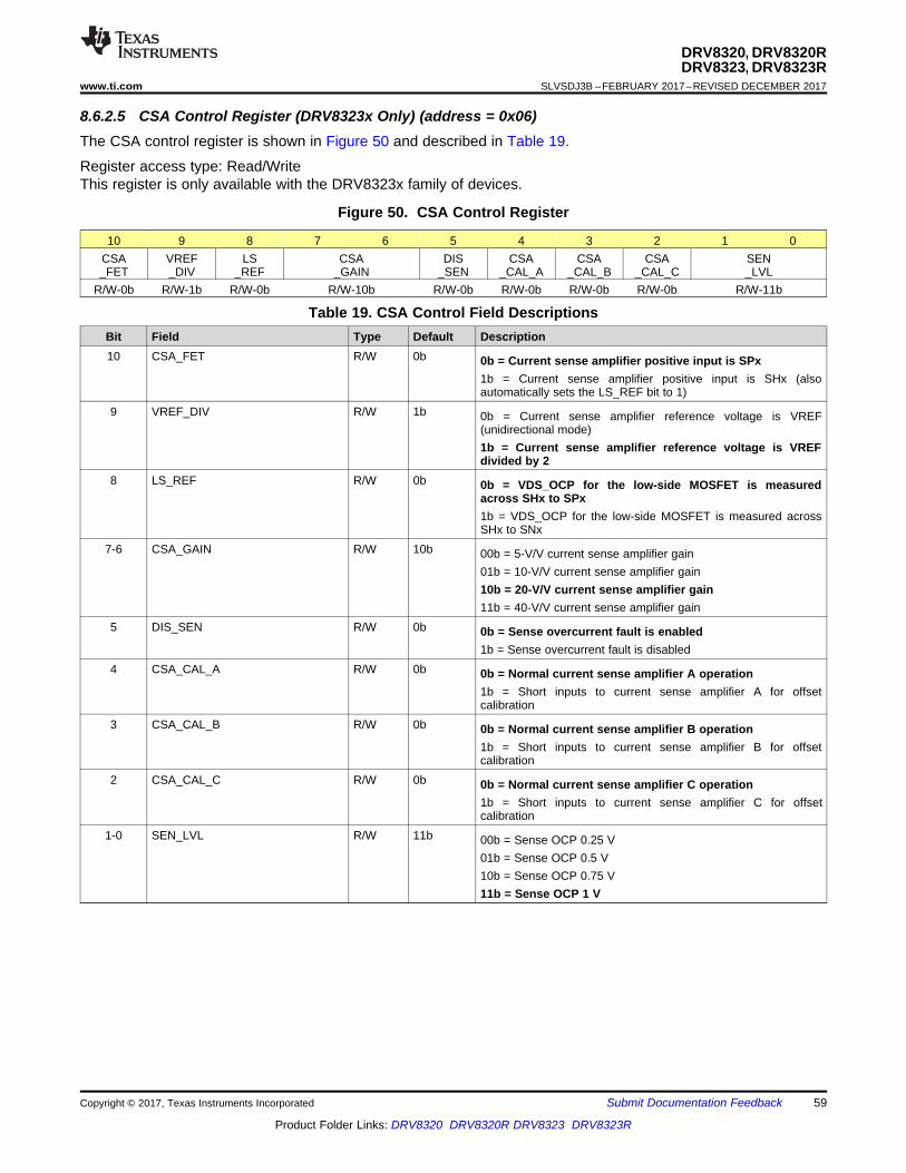
59
DRV8320, DRV8320RDRV8323, DRV8323R
www.ti.com SLVSDJ3B –FEBRUARY 2017–REVISED DECEMBER 2017
Product Folder Links: DRV8320 DRV8320R DRV8323 DRV8323R
Submit Documentation FeedbackCopyright © 2017, Texas Instruments Incorporated
8.6.2.5 CSA Control Register (DRV8323x Only) (address = 0x06)The CSA control register is shown in Figure 50 and described in Table 19.
Register access type: Read/WriteThis register is only available with the DRV8323x family of devices.
Figure 50. CSA Control Register
10 9 8 7 6 5 4 3 2 1 0CSA_FET
VREF_DIV
LS_REF
CSA_GAIN
DIS_SEN
CSA_CAL_A
CSA_CAL_B
CSA_CAL_C
SEN_LVL
R/W-0b R/W-1b R/W-0b R/W-10b R/W-0b R/W-0b R/W-0b R/W-0b R/W-11b
Table 19. CSA Control Field DescriptionsBit Field Type Default Description10 CSA_FET R/W 0b 0b = Current sense amplifier positive input is SPx
1b = Current sense amplifier positive input is SHx (alsoautomatically sets the LS_REF bit to 1)
9 VREF_DIV R/W 1b 0b = Current sense amplifier reference voltage is VREF(unidirectional mode)1b = Current sense amplifier reference voltage is VREFdivided by 2
8 LS_REF R/W 0b 0b = VDS_OCP for the low-side MOSFET is measuredacross SHx to SPx1b = VDS_OCP for the low-side MOSFET is measured acrossSHx to SNx
7-6 CSA_GAIN R/W 10b 00b = 5-V/V current sense amplifier gain01b = 10-V/V current sense amplifier gain10b = 20-V/V current sense amplifier gain11b = 40-V/V current sense amplifier gain
5 DIS_SEN R/W 0b 0b = Sense overcurrent fault is enabled1b = Sense overcurrent fault is disabled
4 CSA_CAL_A R/W 0b 0b = Normal current sense amplifier A operation1b = Short inputs to current sense amplifier A for offsetcalibration
3 CSA_CAL_B R/W 0b 0b = Normal current sense amplifier B operation1b = Short inputs to current sense amplifier B for offsetcalibration
2 CSA_CAL_C R/W 0b 0b = Normal current sense amplifier C operation1b = Short inputs to current sense amplifier C for offsetcalibration
1-0 SEN_LVL R/W 11b 00b = Sense OCP 0.25 V01b = Sense OCP 0.5 V10b = Sense OCP 0.75 V11b = Sense OCP 1 V
60
DRV8320, DRV8320RDRV8323, DRV8323RSLVSDJ3B –FEBRUARY 2017–REVISED DECEMBER 2017 www.ti.com
Product Folder Links: DRV8320 DRV8320R DRV8323 DRV8323R
Submit Documentation Feedback Copyright © 2017, Texas Instruments Incorporated
9 Application and Implementation
NOTEInformation in the following applications sections is not part of the TI componentspecification, and TI does not warrant its accuracy or completeness. TI’s customers areresponsible for determining suitability of components for their purposes. Customers shouldvalidate and test their design implementation to confirm system functionality.
9.1 Application InformationThe DRV832x family of devices is primarily used in applications for three-phase brushless DC motor control. Thedesign procedures in the Typical Application section highlight how to use and configure the DRV832x family ofdevices.
9.2 Typical Application
9.2.1 Primary ApplicationThe DRV8323R SPI device is used in this application example.
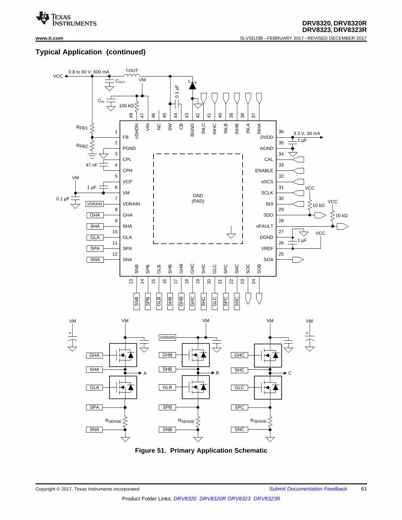
PGND2
FB1
CPH4
CPL3
VM6
VCP5
GHA8
VDRAIN7
GLA10
SHA9
SNA12
SPA11
SP
B14
SN
B13
SH
B16
GLB
15
GH
C18
GH
B17
GLC
20S
HC
19
SN
C22
SP
C21
SO
B24
SO
C23
INLA
47
INH
A
48
INLB
45
INH
B
46
INLC
43
INH
C
44C
B
41
BG
ND
42
NC
39
SW
40
nSH
DN
37
VIN
38
AGND35
DVDD36
ENABLE33
CAL34
SCLK31
nSCS32
SDO29
SDI30
DGND27
nFAULT28
SOA25
VREF26
GND(PAD)
VM
0.8 to 60 V, 600 mA LOUT
3.3 V, 30 mA
VDRAIN
GHA
SHA
GLA
SPA
SNA
SP
B
GLB
SH
B
GH
B
GH
C
SH
C
GLC
SP
C
GHA
SHA
GLA
SPA
SNA
VM
VDRAIN
GHB
SHB
GLB
SPB
VM
GHC
SHC
GLC
SPC
VM
A B C
VM
VM
+ +
VM
VCC
VCC
VCC
100 k
RFB1
RFB2
CIN
COUT
0.1
µF
47 nF
1 µF
0.1 µF
1 µF
10 k VCC
10 k
1 µF
RSENSE
SN
B
SN
C
SNB
RSENSE
SNC
RSENSE
61
DRV8320, DRV8320RDRV8323, DRV8323R
www.ti.com SLVSDJ3B –FEBRUARY 2017–REVISED DECEMBER 2017
Product Folder Links: DRV8320 DRV8320R DRV8323 DRV8323R
Submit Documentation FeedbackCopyright © 2017, Texas Instruments Incorporated
Typical Application (continued)
Figure 51. Primary Application Schematic
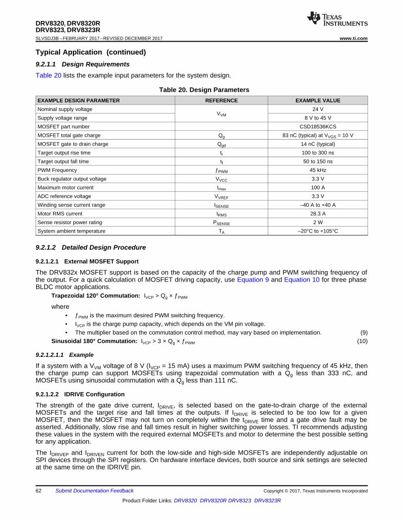
62
DRV8320, DRV8320RDRV8323, DRV8323RSLVSDJ3B –FEBRUARY 2017–REVISED DECEMBER 2017 www.ti.com
Product Folder Links: DRV8320 DRV8320R DRV8323 DRV8323R
Submit Documentation Feedback Copyright © 2017, Texas Instruments Incorporated
Typical Application (continued)9.2.1.1 Design RequirementsTable 20 lists the example input parameters for the system design.
Table 20. Design ParametersEXAMPLE DESIGN PARAMETER REFERENCE EXAMPLE VALUENominal supply voltage
VVM24 V
Supply voltage range 8 V to 45 VMOSFET part number CSD18536KCSMOSFET total gate charge Qg 83 nC (typical) at VVGS = 10 VMOSFET gate to drain charge Qgd 14 nC (typical)Target output rise time tr 100 to 300 nsTarget output fall time tf 50 to 150 nsPWM Frequency ƒPWM 45 kHzBuck regulator output voltage VVCC 3.3 VMaximum motor current Imax 100 AADC reference voltage VVREF 3.3 VWinding sense current range ISENSE –40 A to +40 AMotor RMS current IRMS 28.3 ASense resistor power rating PSENSE 2 WSystem ambient temperature TA –20°C to +105°C
9.2.1.2 Detailed Design Procedure
9.2.1.2.1 External MOSFET Support
The DRV832x MOSFET support is based on the capacity of the charge pump and PWM switching frequency ofthe output. For a quick calculation of MOSFET driving capacity, use Equation 9 and Equation 10 for three phaseBLDC motor applications.
Trapezoidal 120° Commutation: IVCP > Qg × ƒPWM
where• ƒPWM is the maximum desired PWM switching frequency.• IVCP is the charge pump capacity, which depends on the VM pin voltage.• The multiplier based on the commutation control method, may vary based on implementation. (9)
Sinusoidal 180° Commutation: IVCP > 3 × Qg × ƒPWM (10)
9.2.1.2.1.1 Example
If a system with a VVM voltage of 8 V (IVCP = 15 mA) uses a maximum PWM switching frequency of 45 kHz, thenthe charge pump can support MOSFETs using trapezoidal commutation with a Qg less than 333 nC, andMOSFETs using sinusoidal commutation with a Qg less than 111 nC.
9.2.1.2.2 IDRIVE Configuration
The strength of the gate drive current, IDRIVE, is selected based on the gate-to-drain charge of the externalMOSFETs and the target rise and fall times at the outputs. If IDRIVE is selected to be too low for a givenMOSFET, then the MOSFET may not turn on completely within the tDRIVE time and a gate drive fault may beasserted. Additionally, slow rise and fall times result in higher switching power losses. TI recommends adjustingthese values in the system with the required external MOSFETs and motor to determine the best possible settingfor any application.
The IDRIVEP and IDRIVEN current for both the low-side and high-side MOSFETs are independently adjustable onSPI devices through the SPI registers. On hardware interface devices, both source and sink settings are selectedat the same time on the IDRIVE pin.
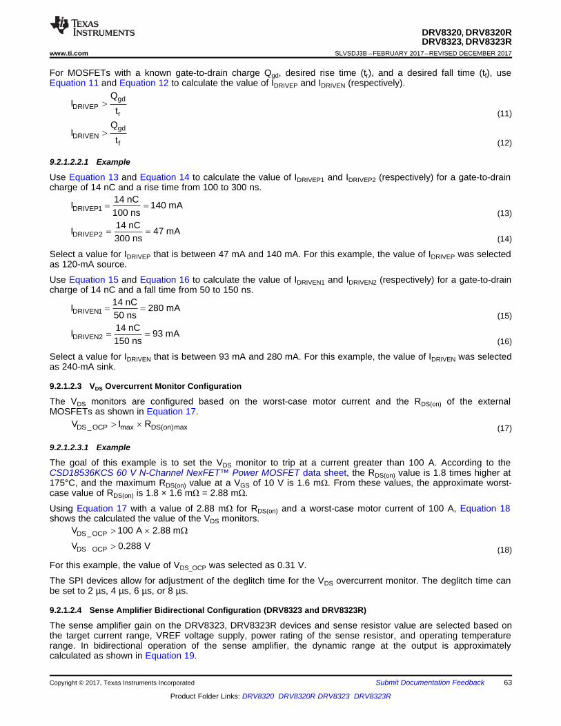
DS _ OCP
DS _ OCP
V 100 A 2.88 m
V 0.288 V
! u :
!
DS _ OCP max DS(on)maxV I R! u
DRIVEN214 nC
I 93 mA150 ns
DRIVEN114 nC
I 280 mA50 ns
DRIVEP214 nC
I 47 mA300 ns
DRIVEP114 nC
I 140 mA100 ns
gdDRIVEN
f
QI
t!
gdDRIVEP
r
QI
t!
63
DRV8320, DRV8320RDRV8323, DRV8323R
www.ti.com SLVSDJ3B –FEBRUARY 2017–REVISED DECEMBER 2017
Product Folder Links: DRV8320 DRV8320R DRV8323 DRV8323R
Submit Documentation FeedbackCopyright © 2017, Texas Instruments Incorporated
For MOSFETs with a known gate-to-drain charge Qgd, desired rise time (tr), and a desired fall time (tf), useEquation 11 and Equation 12 to calculate the value of IDRIVEP and IDRIVEN (respectively).
(11)
(12)
9.2.1.2.2.1 Example
Use Equation 13 and Equation 14 to calculate the value of IDRIVEP1 and IDRIVEP2 (respectively) for a gate-to-draincharge of 14 nC and a rise time from 100 to 300 ns.
(13)
(14)
Select a value for IDRIVEP that is between 47 mA and 140 mA. For this example, the value of IDRIVEP was selectedas 120-mA source.
Use Equation 15 and Equation 16 to calculate the value of IDRIVEN1 and IDRIVEN2 (respectively) for a gate-to-draincharge of 14 nC and a fall time from 50 to 150 ns.
(15)
(16)
Select a value for IDRIVEN that is between 93 mA and 280 mA. For this example, the value of IDRIVEN was selectedas 240-mA sink.
9.2.1.2.3 VDS Overcurrent Monitor Configuration
The VDS monitors are configured based on the worst-case motor current and the RDS(on) of the externalMOSFETs as shown in Equation 17.
(17)
9.2.1.2.3.1 Example
The goal of this example is to set the VDS monitor to trip at a current greater than 100 A. According to theCSD18536KCS 60 V N-Channel NexFET™ Power MOSFET data sheet, the RDS(on) value is 1.8 times higher at175°C, and the maximum RDS(on) value at a VGS of 10 V is 1.6 mΩ. From these values, the approximate worst-case value of RDS(on) is 1.8 × 1.6 mΩ = 2.88 mΩ.
Using Equation 17 with a value of 2.88 mΩ for RDS(on) and a worst-case motor current of 100 A, Equation 18shows the calculated the value of the VDS monitors.
(18)
For this example, the value of VDS_OCP was selected as 0.31 V.
The SPI devices allow for adjustment of the deglitch time for the VDS overcurrent monitor. The deglitch time canbe set to 2 µs, 4 µs, 6 µs, or 8 µs.
9.2.1.2.4 Sense Amplifier Bidirectional Configuration (DRV8323 and DRV8323R)
The sense amplifier gain on the DRV8323, DRV8323R devices and sense resistor value are selected based onthe target current range, VREF voltage supply, power rating of the sense resistor, and operating temperaturerange. In bidirectional operation of the sense amplifier, the dynamic range at the output is approximatelycalculated as shown in Equation 19.
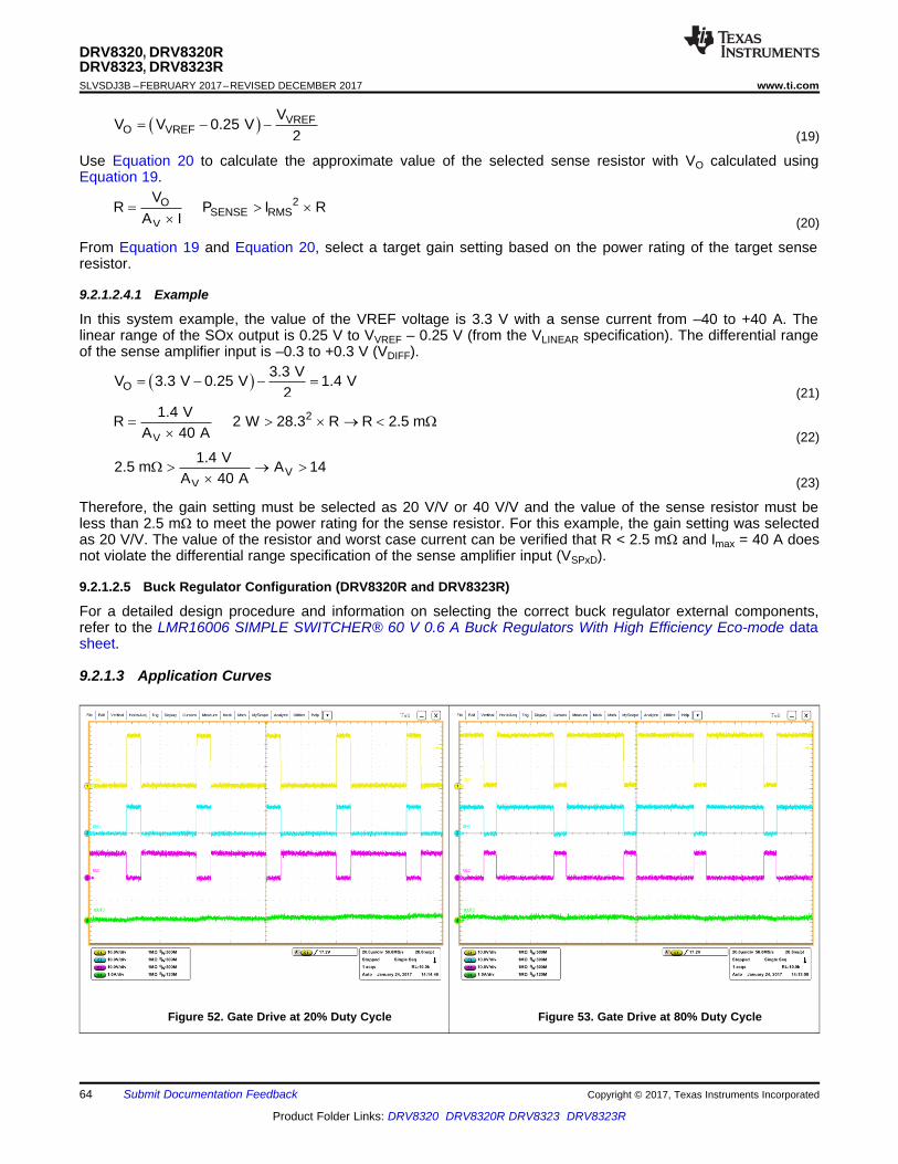
VV
1.4 V2.5 m A 14
A 40 A: ! o !
u
2
V
1.4 VR 2 W 28.3 R R 2.5 m
A 40 A ! u o � :
u
� �O3.3 V
V 3.3 V 0.25 V 1.4 V2
� �
2OSENSE RMS
V
VR P I R
A I ! u
u
� � VREFO VREF
VV V 0.25 V
2 � �
64
DRV8320, DRV8320RDRV8323, DRV8323RSLVSDJ3B –FEBRUARY 2017–REVISED DECEMBER 2017 www.ti.com
Product Folder Links: DRV8320 DRV8320R DRV8323 DRV8323R
Submit Documentation Feedback Copyright © 2017, Texas Instruments Incorporated
(19)
Use Equation 20 to calculate the approximate value of the selected sense resistor with VO calculated usingEquation 19.
(20)
From Equation 19 and Equation 20, select a target gain setting based on the power rating of the target senseresistor.
9.2.1.2.4.1 Example
In this system example, the value of the VREF voltage is 3.3 V with a sense current from –40 to +40 A. Thelinear range of the SOx output is 0.25 V to VVREF – 0.25 V (from the VLINEAR specification). The differential rangeof the sense amplifier input is –0.3 to +0.3 V (VDIFF).
(21)
(22)
(23)
Therefore, the gain setting must be selected as 20 V/V or 40 V/V and the value of the sense resistor must beless than 2.5 mΩ to meet the power rating for the sense resistor. For this example, the gain setting was selectedas 20 V/V. The value of the resistor and worst case current can be verified that R < 2.5 mΩ and Imax = 40 A doesnot violate the differential range specification of the sense amplifier input (VSPxD).
9.2.1.2.5 Buck Regulator Configuration (DRV8320R and DRV8323R)
For a detailed design procedure and information on selecting the correct buck regulator external components,refer to the LMR16006 SIMPLE SWITCHER® 60 V 0.6 A Buck Regulators With High Efficiency Eco-mode datasheet.
9.2.1.3 Application Curves
Figure 52. Gate Drive at 20% Duty Cycle Figure 53. Gate Drive at 80% Duty Cycle
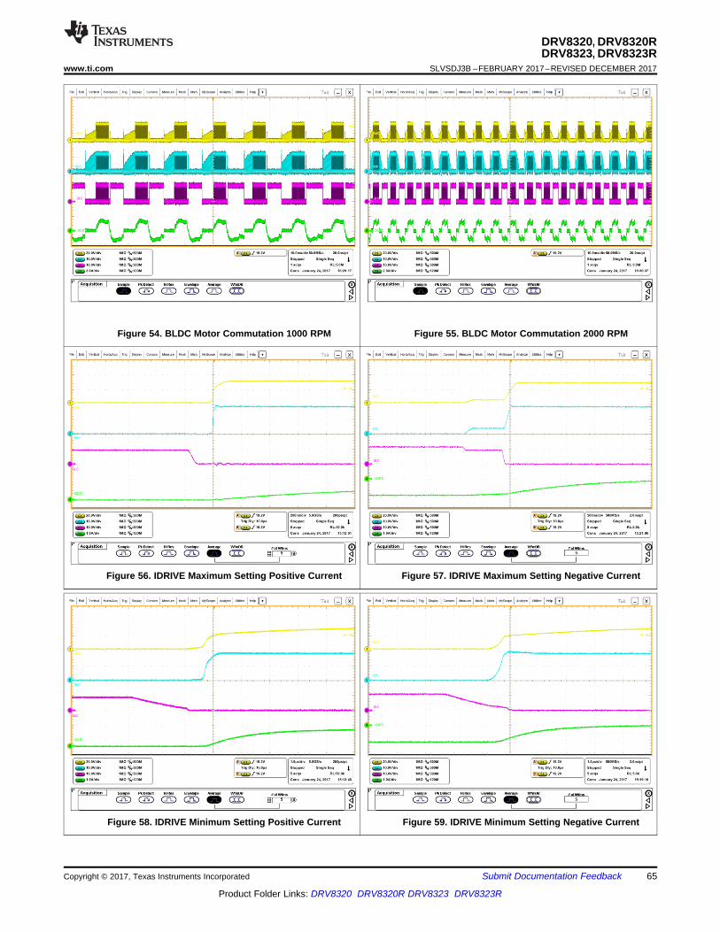
65
DRV8320, DRV8320RDRV8323, DRV8323R
www.ti.com SLVSDJ3B –FEBRUARY 2017–REVISED DECEMBER 2017
Product Folder Links: DRV8320 DRV8320R DRV8323 DRV8323R
Submit Documentation FeedbackCopyright © 2017, Texas Instruments Incorporated
Figure 54. BLDC Motor Commutation 1000 RPM Figure 55. BLDC Motor Commutation 2000 RPM
Figure 56. IDRIVE Maximum Setting Positive Current Figure 57. IDRIVE Maximum Setting Negative Current
Figure 58. IDRIVE Minimum Setting Positive Current Figure 59. IDRIVE Minimum Setting Negative Current
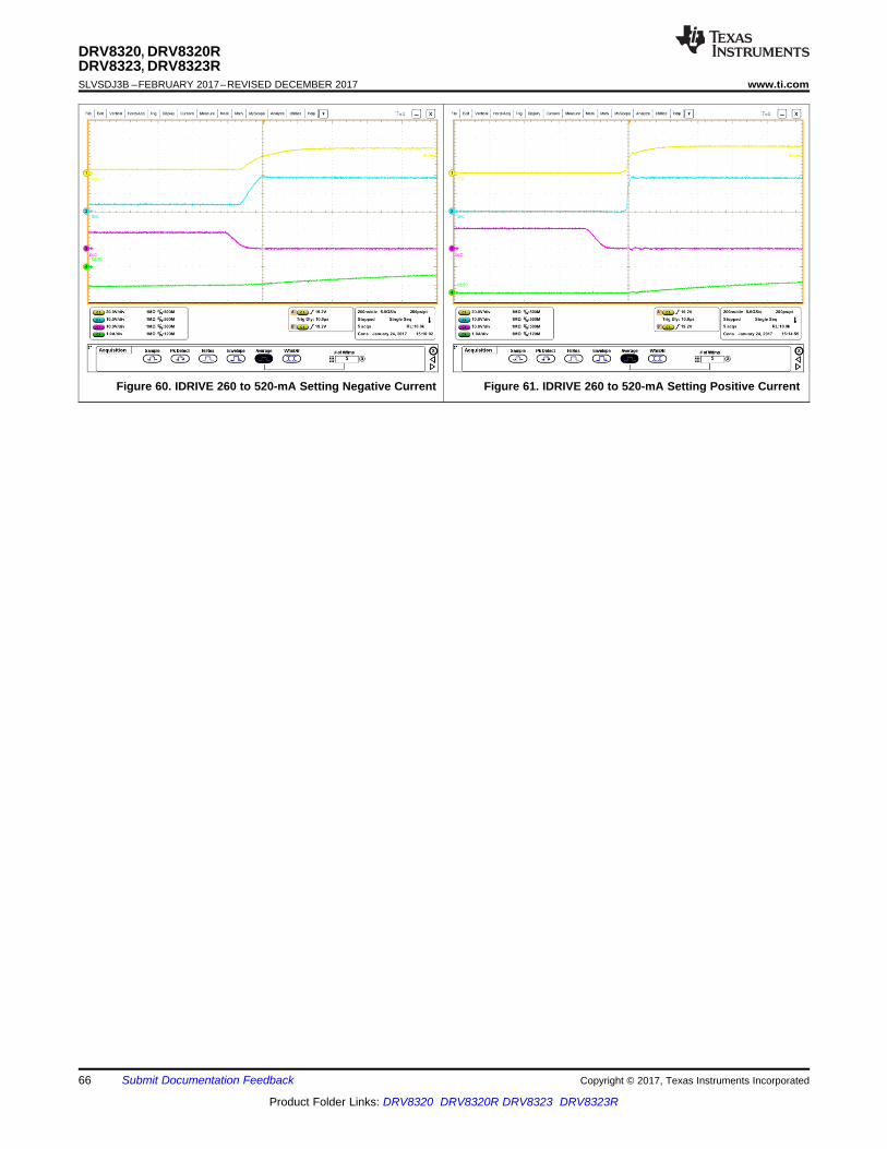
66
DRV8320, DRV8320RDRV8323, DRV8323RSLVSDJ3B –FEBRUARY 2017–REVISED DECEMBER 2017 www.ti.com
Product Folder Links: DRV8320 DRV8320R DRV8323 DRV8323R
Submit Documentation Feedback Copyright © 2017, Texas Instruments Incorporated
Figure 60. IDRIVE 260 to 520-mA Setting Negative Current Figure 61. IDRIVE 260 to 520-mA Setting Positive Current
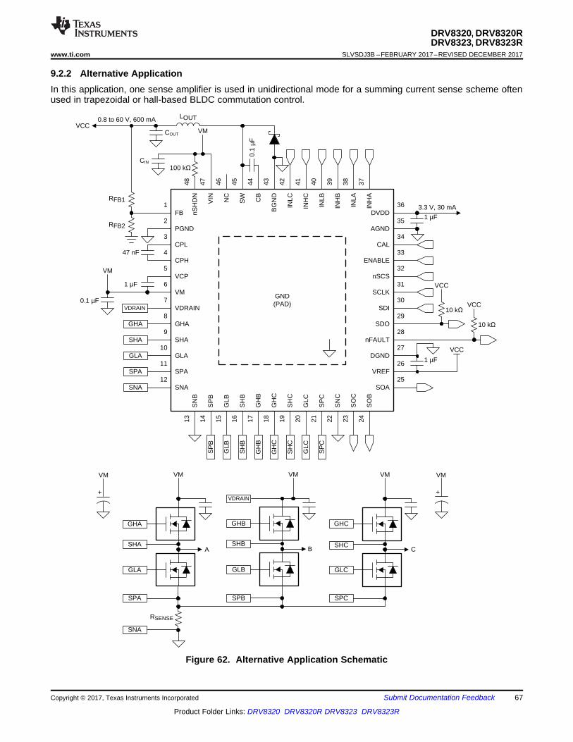
PGND2
FB1
CPH4
CPL3
VM6
VCP5
GHA8
VDRAIN7
GLA10
SHA9
SNA12
SPA11
SP
B14
SN
B13
SH
B16
GLB
15
GH
C18
GH
B17
GLC
20S
HC
19
SN
C22
SP
C21
SO
B24
SO
C23
INLA
47
INH
A
48
INLB
45
INH
B
46
INLC
43
INH
C
44C
B
41
BG
ND
42
NC
39
SW
40
nSH
DN
37
VIN
38
AGND35
DVDD36
ENABLE33
CAL34
SCLK31
nSCS32
SDO29
SDI30
DGND27
nFAULT28
SOA25
VREF26
GND(PAD)
VM
0.8 to 60 V, 600 mA LOUT
3.3 V, 30 mA
VDRAIN
GHA
SHA
GLA
SPA
SNA
SP
B
GLB
SH
B
GH
B
GH
C
SH
C
GLC
SP
C
GHA
SHA
GLA
SPA
SNA
VM
VDRAIN
GHB
SHB
GLB
SPB
VM
GHC
SHC
GLC
SPC
VM
A B C
VM
VM
+ +
VM
VCC
VCC
VCC
100 k
RFB1
RFB2
CIN
COUT
0.1
µF
47 nF
1 µF
0.1 µF
1 µF
10 k VCC
10 k
1 µF
RSENSE
67
DRV8320, DRV8320RDRV8323, DRV8323R
www.ti.com SLVSDJ3B –FEBRUARY 2017–REVISED DECEMBER 2017
Product Folder Links: DRV8320 DRV8320R DRV8323 DRV8323R
Submit Documentation FeedbackCopyright © 2017, Texas Instruments Incorporated
9.2.2 Alternative ApplicationIn this application, one sense amplifier is used in unidirectional mode for a summing current sense scheme oftenused in trapezoidal or hall-based BLDC commutation control.
Figure 62. Alternative Application Schematic
VV
2.8 V3.75 m A 18.7
A 40 A: ! o !
u
2
V
2.8 VR 3 W 28.3 R R 3.75 m
A 40 A ! u o � :
u
OV 3.3 V 0.5 V 2.8 V �
O VREFV V 0.5 V �
2OSENSE RMS
V
VR P I R
A I ! u
u
� �O VREF VREFV V 0.25 V 0.25 V V 0.5 V � � �
68
DRV8320, DRV8320RDRV8323, DRV8323RSLVSDJ3B –FEBRUARY 2017–REVISED DECEMBER 2017 www.ti.com
Product Folder Links: DRV8320 DRV8320R DRV8323 DRV8323R
Submit Documentation Feedback Copyright © 2017, Texas Instruments Incorporated
9.2.2.1 Design RequirementsTable 21 lists the example design input parameters for system design.
Table 21. Design ParametersEXAMPLE DESIGN PARAMETER REFERENCE EXAMPLE VALUEADC reference voltage VVREF 3.3 VSensed current ISENSE 0 to 40 AMotor RMS current IRMS 28.3 ASense-resistor power rating PSENSE 3 WSystem ambient temperature TA –20°C to +105°C
9.2.2.2 Detailed Design Procedure
9.2.2.2.1 Sense Amplifier Unidirectional Configuration
The sense amplifiers are configured to be unidirectional through the registers on SPI devices by writing a 0 to theVREF_DIV bit.
The sense amplifier gain and sense resistor values are selected based on the target current range, VREF, powerrating of the sense resistor, and operating temperature range. In unidirectional operation of the sense amplifier,use Equation 24 to calculate the approximate value of the dynamic range at the output.
(24)
Use Equation 25 to calculate the approximate value of the selected sense resistor.
where• (25)
From Equation 24 and Equation 25, select a target gain setting based on the power rating of a target senseresistor.
9.2.2.2.1.1 Example
In this system example, the value of the VREF voltage is 3.3 V with a sense current from 0 to 40 A. The linearrange of the SOx output for the DRV8323x device is 0.25 V to VVREF – 0.25 V (from the VLINEAR specification).The differential range of the sense-amplifier input is –0.3 to +0.3 V (VDIFF).
(26)
(27)
(28)
Therefore, the gain setting must be selected as 20 V/V or 40 V/V and the value of the sense resistor must beless than 3.75 mΩ to meet the power rating for the sense resistor. For this example, the gain setting wasselected as 20 V/V. The value of the resistor and worst-case current can be verified that R < 3.75 mΩ and Imax =40 A does not violate the differential range specification of the sense amplifier input (VSPxD).
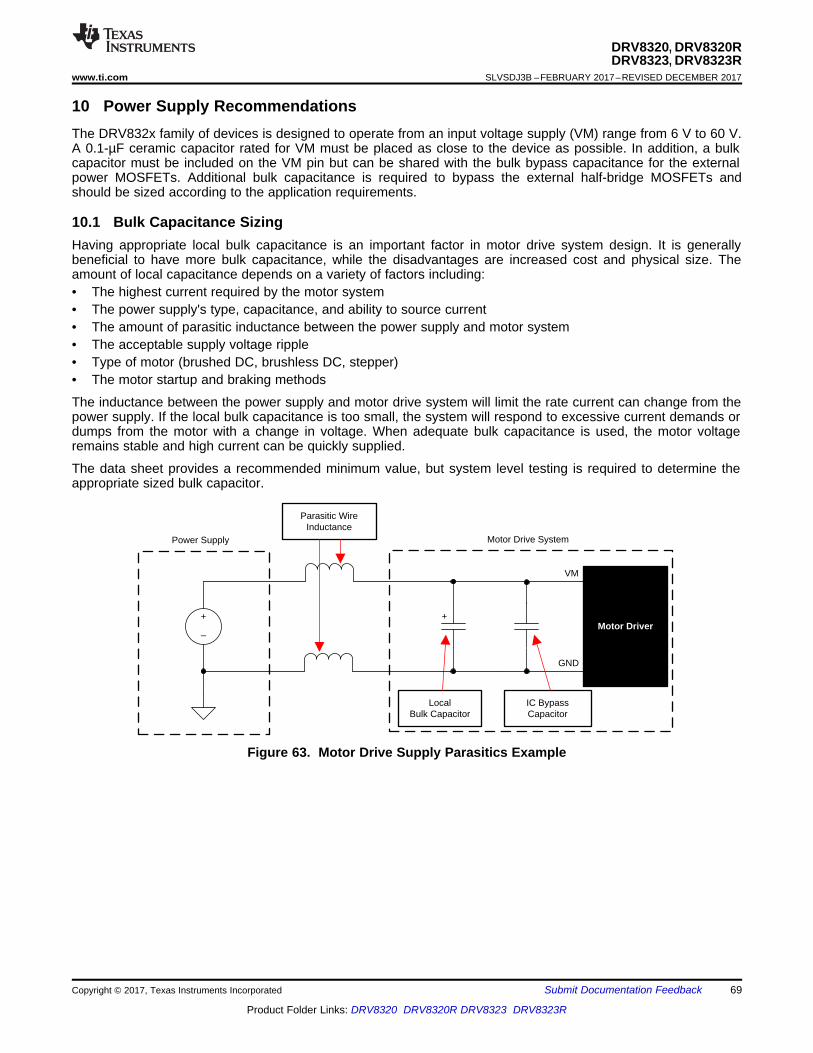
Local Bulk Capacitor
Parasitic WireInductance
+
±
Motor Driver
Power Supply Motor Drive System
VM
GND
+
IC BypassCapacitor
69
DRV8320, DRV8320RDRV8323, DRV8323R
www.ti.com SLVSDJ3B –FEBRUARY 2017–REVISED DECEMBER 2017
Product Folder Links: DRV8320 DRV8320R DRV8323 DRV8323R
Submit Documentation FeedbackCopyright © 2017, Texas Instruments Incorporated
10 Power Supply RecommendationsThe DRV832x family of devices is designed to operate from an input voltage supply (VM) range from 6 V to 60 V.A 0.1-µF ceramic capacitor rated for VM must be placed as close to the device as possible. In addition, a bulkcapacitor must be included on the VM pin but can be shared with the bulk bypass capacitance for the externalpower MOSFETs. Additional bulk capacitance is required to bypass the external half-bridge MOSFETs andshould be sized according to the application requirements.
10.1 Bulk Capacitance SizingHaving appropriate local bulk capacitance is an important factor in motor drive system design. It is generallybeneficial to have more bulk capacitance, while the disadvantages are increased cost and physical size. Theamount of local capacitance depends on a variety of factors including:• The highest current required by the motor system• The power supply's type, capacitance, and ability to source current• The amount of parasitic inductance between the power supply and motor system• The acceptable supply voltage ripple• Type of motor (brushed DC, brushless DC, stepper)• The motor startup and braking methods
The inductance between the power supply and motor drive system will limit the rate current can change from thepower supply. If the local bulk capacitance is too small, the system will respond to excessive current demands ordumps from the motor with a change in voltage. When adequate bulk capacitance is used, the motor voltageremains stable and high current can be quickly supplied.
The data sheet provides a recommended minimum value, but system level testing is required to determine theappropriate sized bulk capacitor.
Figure 63. Motor Drive Supply Parasitics Example
70
DRV8320, DRV8320RDRV8323, DRV8323RSLVSDJ3B –FEBRUARY 2017–REVISED DECEMBER 2017 www.ti.com
Product Folder Links: DRV8320 DRV8320R DRV8323 DRV8323R
Submit Documentation Feedback Copyright © 2017, Texas Instruments Incorporated
11 Layout
11.1 Layout GuidelinesBypass the VM pin to the PGND pin using a low-ESR ceramic bypass capacitor with a recommended value of0.1 µF. Place this capacitor as close to the VM pin as possible with a thick trace or ground plane connected tothe PGND pin. Additionally, bypass the VM pin using a bulk capacitor rated for VM. This component can beelectrolytic. This capacitance must be at least 10 µF.
Additional bulk capacitance is required to bypass the high current path on the external MOSFETs. This bulkcapacitance should be placed such that it minimizes the length of any high current paths through the externalMOSFETs. The connecting metal traces should be as wide as possible, with numerous vias connecting PCBlayers. These practices minimize inductance and let the bulk capacitor deliver high current.
Place a low-ESR ceramic capacitor between the CPL and CPH pins. This capacitor should be 47 nF, rated forVM, and be of type X5R or X7R. Additionally, place a low-ESR ceramic capacitor between the VCP and VM pins.This capacitor should be 1 µF, rated for 16 V, and be of type X5R or X7R.
Bypass the DVDD pin to the AGND pin with a 1-µF low-ESR ceramic capacitor rated for 6.3 V and of type X5Ror X7R. Place this capacitor as close to the pin as possible and minimize the path from the capacitor to theAGND pin.
The VDRAIN pin can be shorted directly to the VM pin. However, if a significant distance is between the deviceand the external MOSFETs, use a dedicated trace to connect to the common point of the drains of the high-sideexternal MOSFETs. Do not connect the SLx pins directly to PGND. Instead, use dedicated traces to connectthese pins to the sources of the low-side external MOSFETs. These recommendations offer more accurate VDSsensing of the external MOSFETs for overcurrent detection.
Minimize the loop length for the high-side and low-side gate drivers. The high-side loop is from the GHx pin ofthe device to the high-side power MOSFET gate, then follows the high-side MOSFET source back to the SHxpin. The low-side loop is from the GLx pin of the device to the low-side power MOSFET gate, then follows thelow-side MOSFET source back to the PGND pin.
11.1.1 Buck-Regulator Layout GuidelinesLayout is a critical portion of good power supply design. The following guidelines help users design a PCB withthe best power conversion performance, thermal performance, and minimized generation of unwantedelectromagnetic interference (EMI):• Place the feedback network resistors close to the FB pin and away from the inductor to minimize coupling
noise into the feedback pin.• Place the input bypass capacitor close to the VIN pin to decrease copper trace resistance which effects the
input voltage ripple of the device.• Place the inductor close to the SW pin to decrease magnetic and electrostatic noise.• Place the output capacitor close to the junction of the inductor and the diode. The inductor, diode, and COUT
trace should be as short as possible to decrease conducted and radiated noise and increase overallefficiency.
• Make the ground connection for the diode, CVIN, and COUT as small as possible and tie it to the systemground plane in only one spot (preferably at the COUT ground point) to minimize conducted noise in thesystem ground plane.
For more detail on switching power supply layout considerations refer to the AN-1149 Layout Guidelines forSwitching Power Supplies application report.
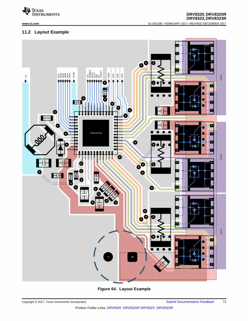
19 SHCThermal Pad
18 GHC
17 GHB
16 SHB
15 GLB
14
13
24
23
22 SNC
21 SPC
20 GLC
6V
M
7V
DR
AIN
8G
HA
9S
HA
10G
LA
11S
PA
12S
NA
1 2 3C
PL
4C
PH
5V
CP
42
43
44
45
46
47
37
38
39
40
41
31 30S
DI
29 28 27 26 2535 34 33 3236
SW
INHA
INLA
INHB
INLB
INHC
INLC
SOB
SPB
SNBnSHDN
VIN
CB
BGND
48
NC
INLC
INH
AIN
HC
INH
BIN
LAIN
HA
DV
DD
CA
LE
NA
BLE
nSC
SS
CLK
SD
IS
OnF
AU
LT
VR
EF
SO
A
SO
B
SO
C
VO
S
S
S
D
D
D
D G
S
S
S
D
D
D
DG
S
S
S
D
D
D
DG
S
S
S
D
D
D
D G
S
S
S
D
D
D
D G
S
S
S
D
D
D
DG
SOC
OU
TC
OU
TB
OU
TA
FB
PG
ND
SC
LK
SD
O
nFA
ULT
DG
ND
AG
ND
CA
L
EN
AB
LE
nSC
S
DV
DD
VR
EF
SO
A
71
DRV8320, DRV8320RDRV8323, DRV8323R
www.ti.com SLVSDJ3B –FEBRUARY 2017–REVISED DECEMBER 2017
Product Folder Links: DRV8320 DRV8320R DRV8323 DRV8323R
Submit Documentation FeedbackCopyright © 2017, Texas Instruments Incorporated
11.2 Layout Example
Figure 64. Layout Example
(RGZ)(2)DRV83
PrefixDRV83 ± Three Phase Brushless DC
(3) (R)
Tape and Reel R ± Tape and Reel T ± Small Tape and Reel
PackageRTV ± 5 × 5 × 0.75 mm QFNRHA ± 6 x 6 × 0.9 mm QFNRTA ± 6 x 6 × 0.75 mm QFNRGZ ± 7 × 7 × 0.9 mm QFN
Series2 ± 60 V device
(R)
Sense amplifiers0 ± No sense amplifiers3 ± 3x sense amplifiers
Buck Regulator[blank] ± No buck regulatorR ± Buck regulator
(S)
InterfaceS ± SPI interfaceH ± Hardware interface
72
DRV8320, DRV8320RDRV8323, DRV8323RSLVSDJ3B –FEBRUARY 2017–REVISED DECEMBER 2017 www.ti.com
Product Folder Links: DRV8320 DRV8320R DRV8323 DRV8323R
Submit Documentation Feedback Copyright © 2017, Texas Instruments Incorporated
12 Device and Documentation Support
12.1 Device Support
12.1.1 Device NomenclatureThe following figure shows a legend for interpreting the complete device name:
12.2 Documentation Support
12.2.1 Related Documentation• Texas Instruments, AN-1149 Layout Guidelines for Switching Power Supplies application report• Texas Instruments, CSD18536KCS 60 V N-Channel NexFET™ Power MOSFET data sheet• Texas Instruments, Hardware Design Considerations for an Efficient Vacuum Cleaner using BLDC Motor• Texas Instruments, Hardware Design Considerations for an Electric Bicycle using BLDC Motor• Texas Instruments, Industrial Motor Drive Solution Guide• Texas Instruments, Layout Guidelines for Switching Power Supplies• Texas Instruments, LMR16006 SIMPLE SWITCHER® 60 V 0.6 A Buck Regulators With High Efficiency Eco-
mode data sheet• Texas Instruments, QFN/SON PCB Attachment application report• Texas Instruments, Sensored 3-Phase BLDC Motor Control Using MSP430™ application report• Texas Instruments, Understanding IDRIVE and TDRIVE In TI Motor Gate Drivers application report
12.3 Related LinksThe table below lists quick access links. Categories include technical documents, support and communityresources, tools and software, and quick access to order now.
Table 22. Related Links
PARTS PRODUCT FOLDER ORDER NOW TECHNICALDOCUMENTS
TOOLS &SOFTWARE
SUPPORT &COMMUNITY
DRV8320 Click here Click here Click here Click here Click hereDRV8320R Click here Click here Click here Click here Click hereDRV8323 Click here Click here Click here Click here Click here
DRV8323R Click here Click here Click here Click here Click here
73
DRV8320, DRV8320RDRV8323, DRV8323R
www.ti.com SLVSDJ3B –FEBRUARY 2017–REVISED DECEMBER 2017
Product Folder Links: DRV8320 DRV8320R DRV8323 DRV8323R
Submit Documentation FeedbackCopyright © 2017, Texas Instruments Incorporated
12.4 Receiving Notification of Documentation UpdatesTo receive notification of documentation updates, navigate to the device product folder on ti.com. In the upperright corner, click on Alert me to register and receive a weekly digest of any product information that haschanged. For change details, review the revision history included in any revised document.
12.5 Community ResourcesThe following links connect to TI community resources. Linked contents are provided "AS IS" by the respectivecontributors. They do not constitute TI specifications and do not necessarily reflect TI's views; see TI's Terms ofUse.
TI E2E™ Online Community TI's Engineer-to-Engineer (E2E) Community. Created to foster collaborationamong engineers. At e2e.ti.com, you can ask questions, share knowledge, explore ideas and helpsolve problems with fellow engineers.
Design Support TI's Design Support Quickly find helpful E2E forums along with design support tools andcontact information for technical support.
12.6 TrademarksEco-mode, NexFET, MSP430, E2E are trademarks of Texas Instruments.SIMPLE SWITCHER is a registered trademark of Texas Instruments.All other trademarks are the property of their respective owners.
12.7 Electrostatic Discharge CautionThis integrated circuit can be damaged by ESD. Texas Instruments recommends that all integrated circuits be handled withappropriate precautions. Failure to observe proper handling and installation procedures can cause damage.
ESD damage can range from subtle performance degradation to complete device failure. Precision integrated circuits may be moresusceptible to damage because very small parametric changes could cause the device not to meet its published specifications.
12.8 GlossarySLYZ022 — TI Glossary.
This glossary lists and explains terms, acronyms, and definitions.
13 Mechanical, Packaging, and Orderable InformationThe following pages include mechanical, packaging, and orderable information. This information is the mostcurrent data available for the designated devices. This data is subject to change without notice and revision ofthis document. For browser-based versions of this data sheet, refer to the left-hand navigation.
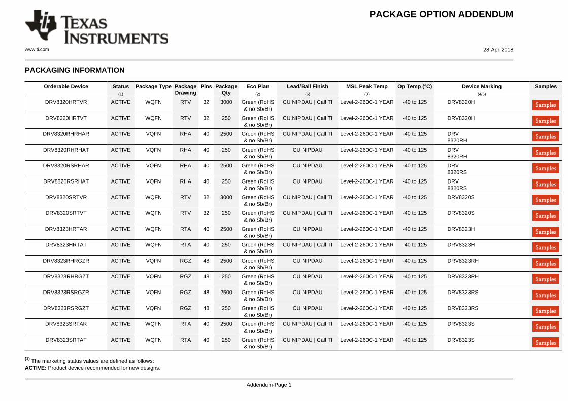
PACKAGE OPTION ADDENDUM
www.ti.com 28-Apr-2018
Addendum-Page 1
PACKAGING INFORMATION
Orderable Device Status(1)
Package Type PackageDrawing
Pins PackageQty
Eco Plan(2)
Lead/Ball Finish(6)
MSL Peak Temp(3)
Op Temp (°C) Device Marking(4/5)
Samples
DRV8320HRTVR ACTIVE WQFN RTV 32 3000 Green (RoHS& no Sb/Br)
CU NIPDAU | Call TI Level-2-260C-1 YEAR -40 to 125 DRV8320H
DRV8320HRTVT ACTIVE WQFN RTV 32 250 Green (RoHS& no Sb/Br)
CU NIPDAU | Call TI Level-2-260C-1 YEAR -40 to 125 DRV8320H
DRV8320RHRHAR ACTIVE VQFN RHA 40 2500 Green (RoHS& no Sb/Br)
CU NIPDAU | Call TI Level-2-260C-1 YEAR -40 to 125 DRV8320RH
DRV8320RHRHAT ACTIVE VQFN RHA 40 250 Green (RoHS& no Sb/Br)
CU NIPDAU Level-2-260C-1 YEAR -40 to 125 DRV8320RH
DRV8320RSRHAR ACTIVE VQFN RHA 40 2500 Green (RoHS& no Sb/Br)
CU NIPDAU Level-2-260C-1 YEAR -40 to 125 DRV8320RS
DRV8320RSRHAT ACTIVE VQFN RHA 40 250 Green (RoHS& no Sb/Br)
CU NIPDAU Level-2-260C-1 YEAR -40 to 125 DRV8320RS
DRV8320SRTVR ACTIVE WQFN RTV 32 3000 Green (RoHS& no Sb/Br)
CU NIPDAU | Call TI Level-2-260C-1 YEAR -40 to 125 DRV8320S
DRV8320SRTVT ACTIVE WQFN RTV 32 250 Green (RoHS& no Sb/Br)
CU NIPDAU | Call TI Level-2-260C-1 YEAR -40 to 125 DRV8320S
DRV8323HRTAR ACTIVE WQFN RTA 40 2500 Green (RoHS& no Sb/Br)
CU NIPDAU Level-2-260C-1 YEAR -40 to 125 DRV8323H
DRV8323HRTAT ACTIVE WQFN RTA 40 250 Green (RoHS& no Sb/Br)
CU NIPDAU | Call TI Level-2-260C-1 YEAR -40 to 125 DRV8323H
DRV8323RHRGZR ACTIVE VQFN RGZ 48 2500 Green (RoHS& no Sb/Br)
CU NIPDAU Level-2-260C-1 YEAR -40 to 125 DRV8323RH
DRV8323RHRGZT ACTIVE VQFN RGZ 48 250 Green (RoHS& no Sb/Br)
CU NIPDAU Level-2-260C-1 YEAR -40 to 125 DRV8323RH
DRV8323RSRGZR ACTIVE VQFN RGZ 48 2500 Green (RoHS& no Sb/Br)
CU NIPDAU Level-2-260C-1 YEAR -40 to 125 DRV8323RS
DRV8323RSRGZT ACTIVE VQFN RGZ 48 250 Green (RoHS& no Sb/Br)
CU NIPDAU Level-2-260C-1 YEAR -40 to 125 DRV8323RS
DRV8323SRTAR ACTIVE WQFN RTA 40 2500 Green (RoHS& no Sb/Br)
CU NIPDAU | Call TI Level-2-260C-1 YEAR -40 to 125 DRV8323S
DRV8323SRTAT ACTIVE WQFN RTA 40 250 Green (RoHS& no Sb/Br)
CU NIPDAU | Call TI Level-2-260C-1 YEAR -40 to 125 DRV8323S
(1) The marketing status values are defined as follows:ACTIVE: Product device recommended for new designs.
PACKAGE OPTION ADDENDUM
www.ti.com 28-Apr-2018
Addendum-Page 2
LIFEBUY: TI has announced that the device will be discontinued, and a lifetime-buy period is in effect.NRND: Not recommended for new designs. Device is in production to support existing customers, but TI does not recommend using this part in a new design.PREVIEW: Device has been announced but is not in production. Samples may or may not be available.OBSOLETE: TI has discontinued the production of the device.
(2) RoHS: TI defines "RoHS" to mean semiconductor products that are compliant with the current EU RoHS requirements for all 10 RoHS substances, including the requirement that RoHS substancedo not exceed 0.1% by weight in homogeneous materials. Where designed to be soldered at high temperatures, "RoHS" products are suitable for use in specified lead-free processes. TI mayreference these types of products as "Pb-Free".RoHS Exempt: TI defines "RoHS Exempt" to mean products that contain lead but are compliant with EU RoHS pursuant to a specific EU RoHS exemption.Green: TI defines "Green" to mean the content of Chlorine (Cl) and Bromine (Br) based flame retardants meet JS709B low halogen requirements of <=1000ppm threshold. Antimony trioxide basedflame retardants must also meet the <=1000ppm threshold requirement.
(3) MSL, Peak Temp. - The Moisture Sensitivity Level rating according to the JEDEC industry standard classifications, and peak solder temperature.
(4) There may be additional marking, which relates to the logo, the lot trace code information, or the environmental category on the device.
(5) Multiple Device Markings will be inside parentheses. Only one Device Marking contained in parentheses and separated by a "~" will appear on a device. If a line is indented then it is a continuationof the previous line and the two combined represent the entire Device Marking for that device.
(6) Lead/Ball Finish - Orderable Devices may have multiple material finish options. Finish options are separated by a vertical ruled line. Lead/Ball Finish values may wrap to two lines if the finishvalue exceeds the maximum column width.
Important Information and Disclaimer:The information provided on this page represents TI's knowledge and belief as of the date that it is provided. TI bases its knowledge and belief on informationprovided by third parties, and makes no representation or warranty as to the accuracy of such information. Efforts are underway to better integrate information from third parties. TI has taken andcontinues to take reasonable steps to provide representative and accurate information but may not have conducted destructive testing or chemical analysis on incoming materials and chemicals.TI and TI suppliers consider certain information to be proprietary, and thus CAS numbers and other limited information may not be available for release.
In no event shall TI's liability arising out of such information exceed the total purchase price of the TI part(s) at issue in this document sold by TI to Customer on an annual basis.
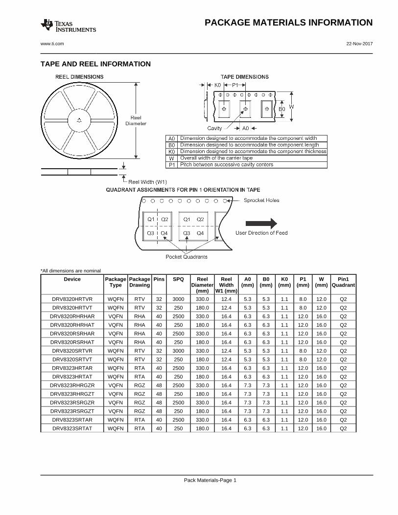
TAPE AND REEL INFORMATION
*All dimensions are nominal
Device PackageType
PackageDrawing
Pins SPQ ReelDiameter
(mm)
ReelWidth
W1 (mm)
A0(mm)
B0(mm)
K0(mm)
P1(mm)
W(mm)
Pin1Quadrant
DRV8320HRTVR WQFN RTV 32 3000 330.0 12.4 5.3 5.3 1.1 8.0 12.0 Q2
DRV8320HRTVT WQFN RTV 32 250 180.0 12.4 5.3 5.3 1.1 8.0 12.0 Q2
DRV8320RHRHAR VQFN RHA 40 2500 330.0 16.4 6.3 6.3 1.1 12.0 16.0 Q2
DRV8320RHRHAT VQFN RHA 40 250 180.0 16.4 6.3 6.3 1.1 12.0 16.0 Q2
DRV8320RSRHAR VQFN RHA 40 2500 330.0 16.4 6.3 6.3 1.1 12.0 16.0 Q2
DRV8320RSRHAT VQFN RHA 40 250 180.0 16.4 6.3 6.3 1.1 12.0 16.0 Q2
DRV8320SRTVR WQFN RTV 32 3000 330.0 12.4 5.3 5.3 1.1 8.0 12.0 Q2
DRV8320SRTVT WQFN RTV 32 250 180.0 12.4 5.3 5.3 1.1 8.0 12.0 Q2
DRV8323HRTAR WQFN RTA 40 2500 330.0 16.4 6.3 6.3 1.1 12.0 16.0 Q2
DRV8323HRTAT WQFN RTA 40 250 180.0 16.4 6.3 6.3 1.1 12.0 16.0 Q2
DRV8323RHRGZR VQFN RGZ 48 2500 330.0 16.4 7.3 7.3 1.1 12.0 16.0 Q2
DRV8323RHRGZT VQFN RGZ 48 250 180.0 16.4 7.3 7.3 1.1 12.0 16.0 Q2
DRV8323RSRGZR VQFN RGZ 48 2500 330.0 16.4 7.3 7.3 1.1 12.0 16.0 Q2
DRV8323RSRGZT VQFN RGZ 48 250 180.0 16.4 7.3 7.3 1.1 12.0 16.0 Q2
DRV8323SRTAR WQFN RTA 40 2500 330.0 16.4 6.3 6.3 1.1 12.0 16.0 Q2
DRV8323SRTAT WQFN RTA 40 250 180.0 16.4 6.3 6.3 1.1 12.0 16.0 Q2
PACKAGE MATERIALS INFORMATION
www.ti.com 22-Nov-2017
Pack Materials-Page 1
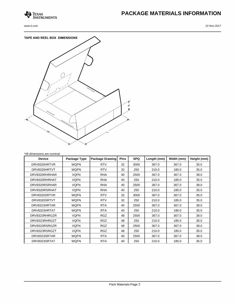
*All dimensions are nominal
Device Package Type Package Drawing Pins SPQ Length (mm) Width (mm) Height (mm)
DRV8320HRTVR WQFN RTV 32 3000 367.0 367.0 35.0
DRV8320HRTVT WQFN RTV 32 250 210.0 185.0 35.0
DRV8320RHRHAR VQFN RHA 40 2500 367.0 367.0 38.0
DRV8320RHRHAT VQFN RHA 40 250 210.0 185.0 35.0
DRV8320RSRHAR VQFN RHA 40 2500 367.0 367.0 38.0
DRV8320RSRHAT VQFN RHA 40 250 210.0 185.0 35.0
DRV8320SRTVR WQFN RTV 32 3000 367.0 367.0 35.0
DRV8320SRTVT WQFN RTV 32 250 210.0 185.0 35.0
DRV8323HRTAR WQFN RTA 40 2500 367.0 367.0 38.0
DRV8323HRTAT WQFN RTA 40 250 210.0 185.0 35.0
DRV8323RHRGZR VQFN RGZ 48 2500 367.0 367.0 38.0
DRV8323RHRGZT VQFN RGZ 48 250 210.0 185.0 35.0
DRV8323RSRGZR VQFN RGZ 48 2500 367.0 367.0 38.0
DRV8323RSRGZT VQFN RGZ 48 250 210.0 185.0 35.0
DRV8323SRTAR WQFN RTA 40 2500 367.0 367.0 38.0
DRV8323SRTAT WQFN RTA 40 250 210.0 185.0 35.0
PACKAGE MATERIALS INFORMATION
www.ti.com 22-Nov-2017
Pack Materials-Page 2
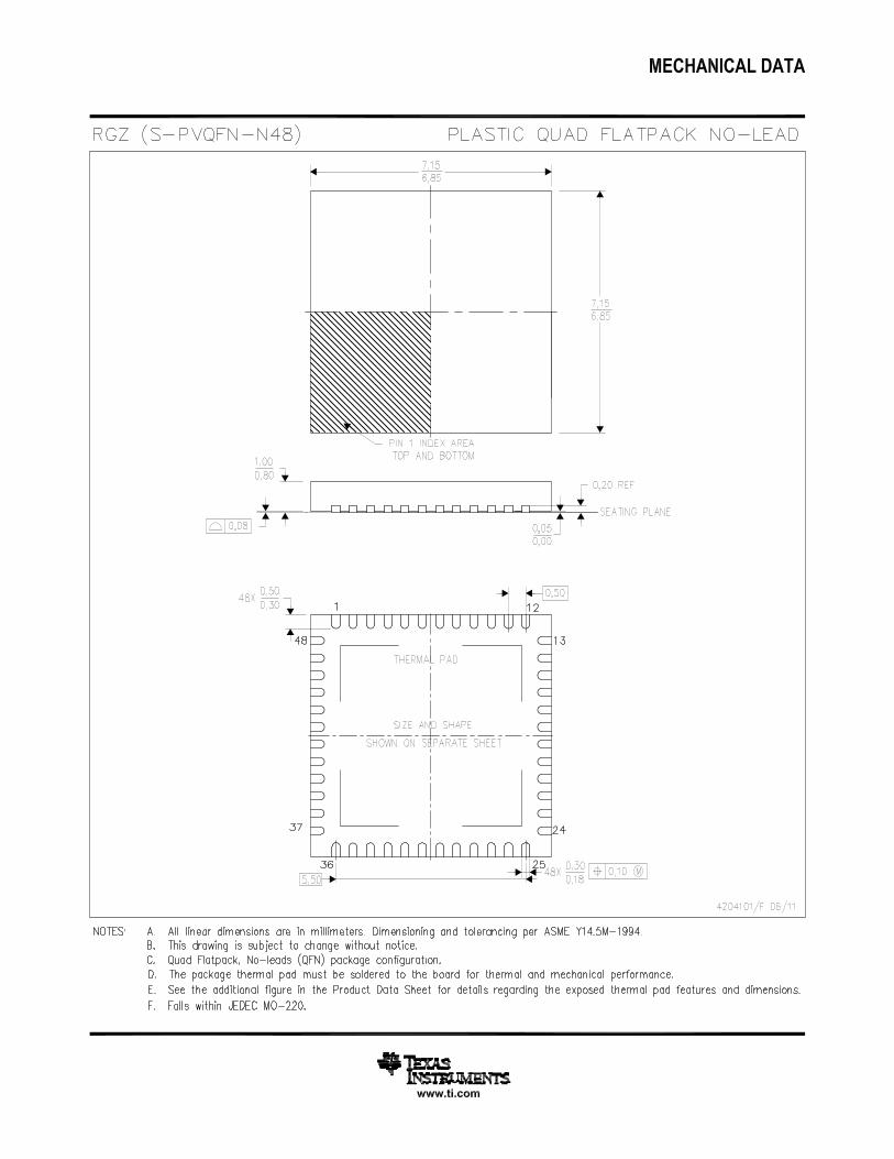
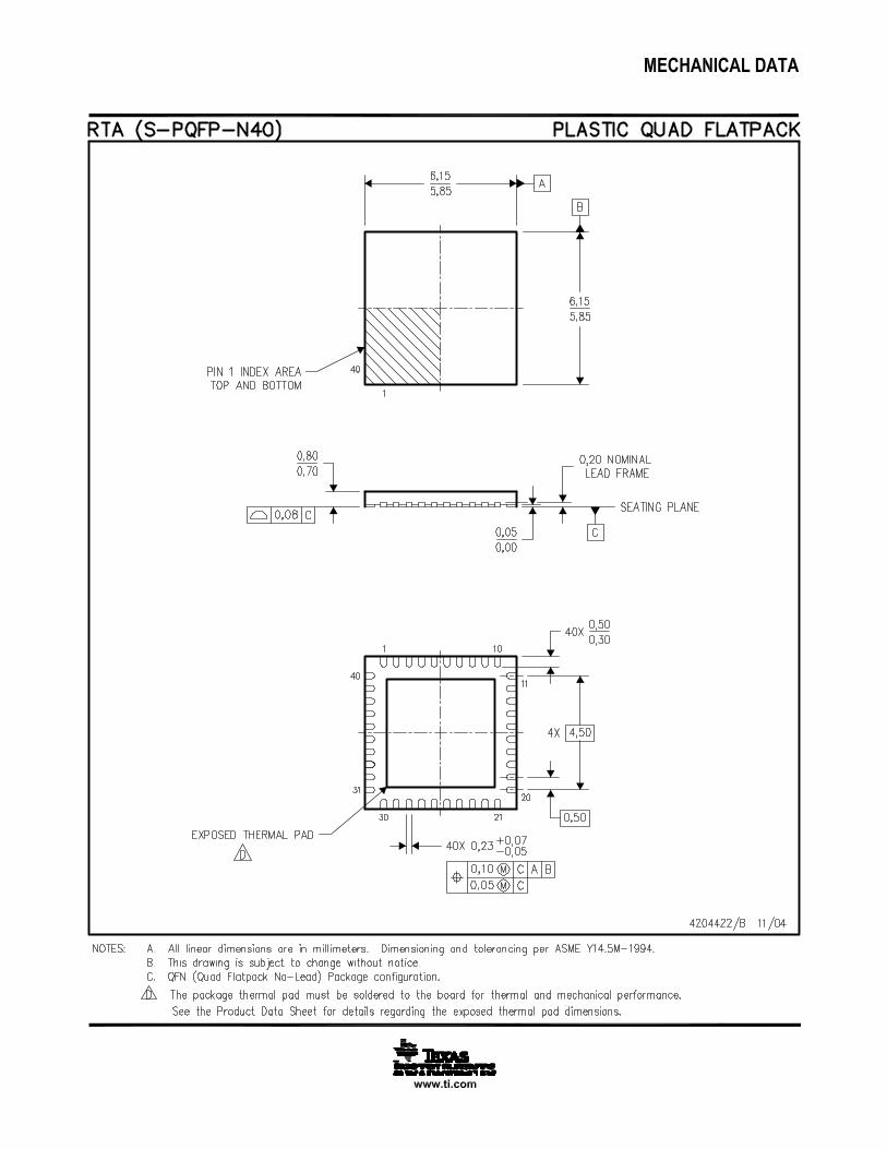
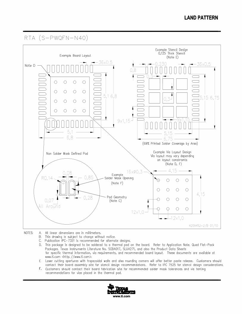
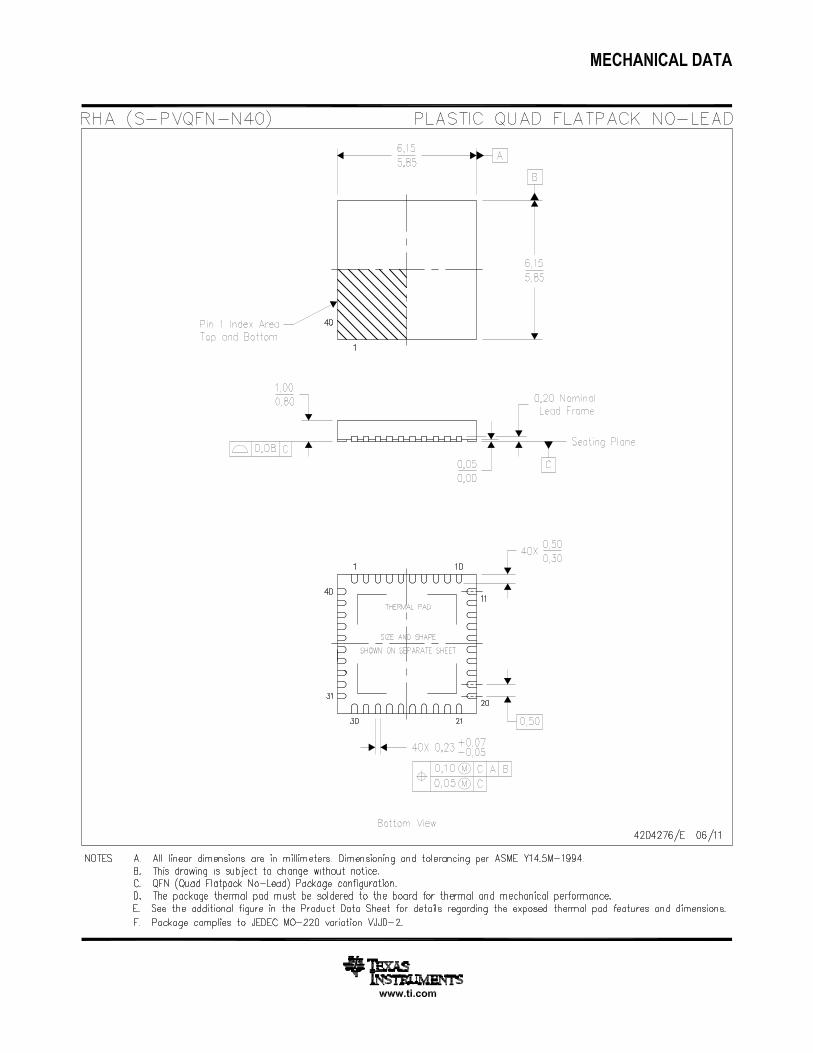
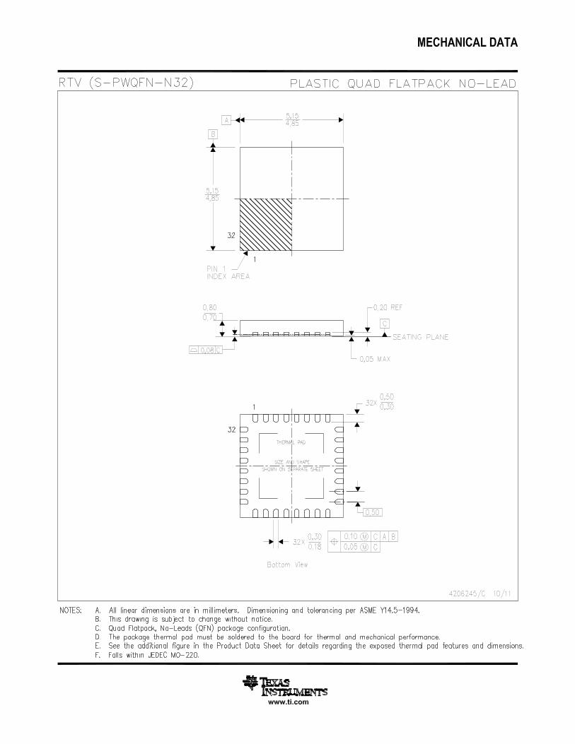
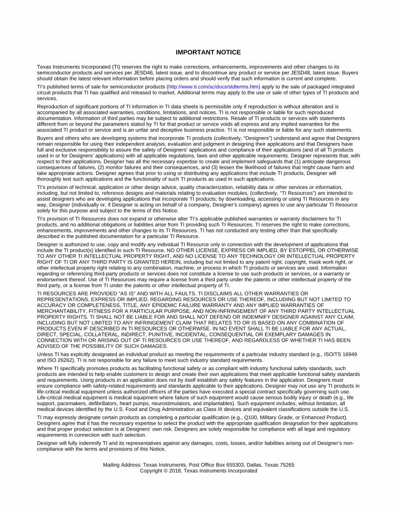
IMPORTANT NOTICE
Texas Instruments Incorporated (TI) reserves the right to make corrections, enhancements, improvements and other changes to itssemiconductor products and services per JESD46, latest issue, and to discontinue any product or service per JESD48, latest issue. Buyersshould obtain the latest relevant information before placing orders and should verify that such information is current and complete.TI’s published terms of sale for semiconductor products (http://www.ti.com/sc/docs/stdterms.htm) apply to the sale of packaged integratedcircuit products that TI has qualified and released to market. Additional terms may apply to the use or sale of other types of TI products andservices.Reproduction of significant portions of TI information in TI data sheets is permissible only if reproduction is without alteration and isaccompanied by all associated warranties, conditions, limitations, and notices. TI is not responsible or liable for such reproduceddocumentation. Information of third parties may be subject to additional restrictions. Resale of TI products or services with statementsdifferent from or beyond the parameters stated by TI for that product or service voids all express and any implied warranties for theassociated TI product or service and is an unfair and deceptive business practice. TI is not responsible or liable for any such statements.Buyers and others who are developing systems that incorporate TI products (collectively, “Designers”) understand and agree that Designersremain responsible for using their independent analysis, evaluation and judgment in designing their applications and that Designers havefull and exclusive responsibility to assure the safety of Designers' applications and compliance of their applications (and of all TI productsused in or for Designers’ applications) with all applicable regulations, laws and other applicable requirements. Designer represents that, withrespect to their applications, Designer has all the necessary expertise to create and implement safeguards that (1) anticipate dangerousconsequences of failures, (2) monitor failures and their consequences, and (3) lessen the likelihood of failures that might cause harm andtake appropriate actions. Designer agrees that prior to using or distributing any applications that include TI products, Designer willthoroughly test such applications and the functionality of such TI products as used in such applications.TI’s provision of technical, application or other design advice, quality characterization, reliability data or other services or information,including, but not limited to, reference designs and materials relating to evaluation modules, (collectively, “TI Resources”) are intended toassist designers who are developing applications that incorporate TI products; by downloading, accessing or using TI Resources in anyway, Designer (individually or, if Designer is acting on behalf of a company, Designer’s company) agrees to use any particular TI Resourcesolely for this purpose and subject to the terms of this Notice.TI’s provision of TI Resources does not expand or otherwise alter TI’s applicable published warranties or warranty disclaimers for TIproducts, and no additional obligations or liabilities arise from TI providing such TI Resources. TI reserves the right to make corrections,enhancements, improvements and other changes to its TI Resources. TI has not conducted any testing other than that specificallydescribed in the published documentation for a particular TI Resource.Designer is authorized to use, copy and modify any individual TI Resource only in connection with the development of applications thatinclude the TI product(s) identified in such TI Resource. NO OTHER LICENSE, EXPRESS OR IMPLIED, BY ESTOPPEL OR OTHERWISETO ANY OTHER TI INTELLECTUAL PROPERTY RIGHT, AND NO LICENSE TO ANY TECHNOLOGY OR INTELLECTUAL PROPERTYRIGHT OF TI OR ANY THIRD PARTY IS GRANTED HEREIN, including but not limited to any patent right, copyright, mask work right, orother intellectual property right relating to any combination, machine, or process in which TI products or services are used. Informationregarding or referencing third-party products or services does not constitute a license to use such products or services, or a warranty orendorsement thereof. Use of TI Resources may require a license from a third party under the patents or other intellectual property of thethird party, or a license from TI under the patents or other intellectual property of TI.TI RESOURCES ARE PROVIDED “AS IS” AND WITH ALL FAULTS. TI DISCLAIMS ALL OTHER WARRANTIES ORREPRESENTATIONS, EXPRESS OR IMPLIED, REGARDING RESOURCES OR USE THEREOF, INCLUDING BUT NOT LIMITED TOACCURACY OR COMPLETENESS, TITLE, ANY EPIDEMIC FAILURE WARRANTY AND ANY IMPLIED WARRANTIES OFMERCHANTABILITY, FITNESS FOR A PARTICULAR PURPOSE, AND NON-INFRINGEMENT OF ANY THIRD PARTY INTELLECTUALPROPERTY RIGHTS. TI SHALL NOT BE LIABLE FOR AND SHALL NOT DEFEND OR INDEMNIFY DESIGNER AGAINST ANY CLAIM,INCLUDING BUT NOT LIMITED TO ANY INFRINGEMENT CLAIM THAT RELATES TO OR IS BASED ON ANY COMBINATION OFPRODUCTS EVEN IF DESCRIBED IN TI RESOURCES OR OTHERWISE. IN NO EVENT SHALL TI BE LIABLE FOR ANY ACTUAL,DIRECT, SPECIAL, COLLATERAL, INDIRECT, PUNITIVE, INCIDENTAL, CONSEQUENTIAL OR EXEMPLARY DAMAGES INCONNECTION WITH OR ARISING OUT OF TI RESOURCES OR USE THEREOF, AND REGARDLESS OF WHETHER TI HAS BEENADVISED OF THE POSSIBILITY OF SUCH DAMAGES.Unless TI has explicitly designated an individual product as meeting the requirements of a particular industry standard (e.g., ISO/TS 16949and ISO 26262), TI is not responsible for any failure to meet such industry standard requirements.Where TI specifically promotes products as facilitating functional safety or as compliant with industry functional safety standards, suchproducts are intended to help enable customers to design and create their own applications that meet applicable functional safety standardsand requirements. Using products in an application does not by itself establish any safety features in the application. Designers mustensure compliance with safety-related requirements and standards applicable to their applications. Designer may not use any TI products inlife-critical medical equipment unless authorized officers of the parties have executed a special contract specifically governing such use.Life-critical medical equipment is medical equipment where failure of such equipment would cause serious bodily injury or death (e.g., lifesupport, pacemakers, defibrillators, heart pumps, neurostimulators, and implantables). Such equipment includes, without limitation, allmedical devices identified by the U.S. Food and Drug Administration as Class III devices and equivalent classifications outside the U.S.TI may expressly designate certain products as completing a particular qualification (e.g., Q100, Military Grade, or Enhanced Product).Designers agree that it has the necessary expertise to select the product with the appropriate qualification designation for their applicationsand that proper product selection is at Designers’ own risk. Designers are solely responsible for compliance with all legal and regulatoryrequirements in connection with such selection.Designer will fully indemnify TI and its representatives against any damages, costs, losses, and/or liabilities arising out of Designer’s non-compliance with the terms and provisions of this Notice.
Mailing Address: Texas Instruments, Post Office Box 655303, Dallas, Texas 75265Copyright © 2018, Texas Instruments Incorporated