
DRV3245Q-Q1 3-Phase Automotive Gate Driver Unit (GDU) … · A Device MCU N-Channel MOSFETs Sense...
12
A Device MCU N-Channel MOSFETs Sense Gate Drive 4.5 to 45 V nFAULT Protection Diagnostics Monitoring Shunt Amplifiers 3-Phase Gate Driver 3(P) + 2(N) 6(Gate) +6(Source) M Shunt Amplifiers 3 SPI 4 PWM 6 Shutdown 2 B Device MCU N-Channel MOSFETs Sense Gate Drive 4.5 to 45 V nFAULT Protection Diagnostics Monitoring Shunt Amplifiers 3-Phase Gate Driver 2(P) + 2(N) 6(Gate) +6(Source) M Shunt Amplifiers 3 SPI 4 PWM 6 Shutdown 2 Phase Comparators Phase Comparators 3 Product Folder Order Now Technical Documents Tools & Software Support & Community An IMPORTANT NOTICE at the end of this data sheet addresses availability, warranty, changes, use in safety-critical applications, intellectual property matters and other important disclaimers. PRODUCTION DATA. DRV3245Q-Q1 SLVSEE3A – NOVEMBER 2017 – REVISED MAY 2018 DRV3245Q-Q1 3-Phase Automotive Gate Driver Unit (GDU) With High Performance Sensing, Protection and Diagnostics 1 1 Features 1• AEC-Q100 Qualified for Automotive Applications: – Device Temperature Grade 1: –40°C to +125°C, T A • SafeTI™ Semiconductor Component – Developed According to the Applicable Requirements of ISO 26262 • 4.5-V to 45-V Operating Voltage • Programmable Peak Gate Drive Currents up to 1A • Charge-Pump Gate Driver for 100% Duty Cycle • Current-Shunt Amplifiers and Phase Comparators – A Device: 3 Current-Shunt Amplifiers and 3- Phase Comparators With Status Through SPI – B Device: 2 Current-Shunt Amplifiers and 3- Phase Comparators With Real-Time Monitor Through Digital Pins • 3-PWM or 6-PWM Input Control up to 20 kHz • Single PWM-Mode Commutation Capability • Supports Both 3.3-V and 5-V Digital Interface • Serial Peripheral Interface (SPI) • Thermally-Enhanced 48-Pin HTQFP • Protection Features: – Internal Regulators, Battery Voltage monitor – SPI CRC – Clock Monitor – Analog Built-In Self Test – Programmable Dead-Time Control – MOSFET Shoot-Through Prevention – MOSFET V DS Overcurrent Monitors – Gate-Source Voltage Real Time Monitor – Overtemperature Warning and Shutdown 2 Applications • 12-V Automotive Motor-Control Applications – Electrical Power Steering (EPS, EHPS) – Electrical Brake and Brake Assist – Transmissions and Pumps 3 Description The DRV3245Q-Q1 device is a FET gate driver IC for three-phase motor-drive applications designed according to the applicable requirements of ISO 26262 for functional safety applications. The device provides three half-bridge drivers each capable of driving a high-side and low-side N-channel MOSFET while also providing sophisticated protection and monitoring of the FETs. A charge-pump driver enables 100% duty cycle and supports low battery voltages during cold-crank operation. The integration of current-sense amplifiers, integrated phase comparators, and SPI-based configuration of the driver and its peripherals enable reduction of the bill of materials (BOM) and space on the printed circuit board (PCB) because of the elimination of most external and passive components. The DRV3245Q-Q1 device also integrates diagnostics and protection for each internal block and provides support for common system diagnostic checks each of which can be instantiated and reported through SPI. This flexibility of the integrated features allows the device to integrate seamlessly into a variety of safety architectures. Device Information (1) PART NUMBER PACKAGE BODY SIZE (NOM) DRV3245Q-Q1 HTQFP (48) 7.00 mm × 7.00 mm (1) For all available packages, see the orderable addendum at the end of the data sheet. Simplified Schematic
Transcript of DRV3245Q-Q1 3-Phase Automotive Gate Driver Unit (GDU) … · A Device MCU N-Channel MOSFETs Sense...

A Device
MC
U
N-C
hann
el M
OS
FE
Ts
Sense
Gate Drive
4.5 to 45 V
nFAULTProtection
DiagnosticsMonitoring
Shunt Amplifiers
3-Phase Gate Driver
3(P) + 2(N)
6(Gate) +6(Source)
M
Shunt Amplifiers
3
SPI
4
PWM
6
Shutdown
2B Device
MC
U
N-C
hann
el M
OS
FE
Ts
Sense
Gate Drive
4.5 to 45 V
nFAULT
ProtectionDiagnosticsMonitoring
Shunt Amplifiers
3-Phase Gate Driver
2(P) + 2(N)
6(Gate) +6(Source)
M
Shunt Amplifiers
3
SPI
4
PWM
6
Shutdown
2
Phase Comparators
PhaseComparators
3
Product
Folder
Order
Now
Technical
Documents
Tools &
Software
Support &Community
An IMPORTANT NOTICE at the end of this data sheet addresses availability, warranty, changes, use in safety-critical applications,intellectual property matters and other important disclaimers. PRODUCTION DATA.
DRV3245Q-Q1SLVSEE3A –NOVEMBER 2017–REVISED MAY 2018
DRV3245Q-Q1 3-Phase Automotive Gate Driver Unit (GDU) With High PerformanceSensing, Protection and Diagnostics
1
1 Features1• AEC-Q100 Qualified for Automotive Applications:
– Device Temperature Grade 1:–40°C to +125°C, TA
• SafeTI™ Semiconductor Component– Developed According to the Applicable
Requirements of ISO 26262• 4.5-V to 45-V Operating Voltage• Programmable Peak Gate Drive Currents up to 1A• Charge-Pump Gate Driver for 100% Duty Cycle• Current-Shunt Amplifiers and Phase Comparators
– A Device: 3 Current-Shunt Amplifiers and 3-Phase Comparators With Status Through SPI
– B Device: 2 Current-Shunt Amplifiers and 3-Phase Comparators With Real-Time MonitorThrough Digital Pins
• 3-PWM or 6-PWM Input Control up to 20 kHz• Single PWM-Mode Commutation Capability• Supports Both 3.3-V and 5-V Digital Interface• Serial Peripheral Interface (SPI)• Thermally-Enhanced 48-Pin HTQFP• Protection Features:
– Internal Regulators, Battery Voltage monitor– SPI CRC– Clock Monitor– Analog Built-In Self Test– Programmable Dead-Time Control– MOSFET Shoot-Through Prevention– MOSFET VDS Overcurrent Monitors– Gate-Source Voltage Real Time Monitor– Overtemperature Warning and Shutdown
2 Applications• 12-V Automotive Motor-Control Applications
– Electrical Power Steering (EPS, EHPS)– Electrical Brake and Brake Assist– Transmissions and Pumps
3 DescriptionThe DRV3245Q-Q1 device is a FET gate driver IC forthree-phase motor-drive applications designedaccording to the applicable requirements of ISO26262 for functional safety applications. The deviceprovides three half-bridge drivers each capable ofdriving a high-side and low-side N-channel MOSFETwhile also providing sophisticated protection andmonitoring of the FETs. A charge-pump driverenables 100% duty cycle and supports low batteryvoltages during cold-crank operation. The integrationof current-sense amplifiers, integrated phasecomparators, and SPI-based configuration of thedriver and its peripherals enable reduction of the billof materials (BOM) and space on the printed circuitboard (PCB) because of the elimination of mostexternal and passive components.
The DRV3245Q-Q1 device also integratesdiagnostics and protection for each internal block andprovides support for common system diagnosticchecks each of which can be instantiated andreported through SPI. This flexibility of the integratedfeatures allows the device to integrate seamlesslyinto a variety of safety architectures.
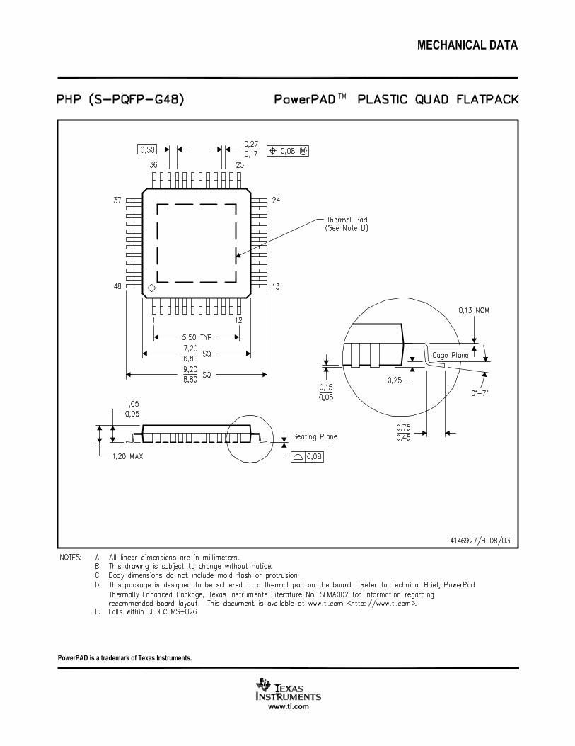
Device Information (1)
PART NUMBER PACKAGE BODY SIZE (NOM)DRV3245Q-Q1 HTQFP (48) 7.00 mm × 7.00 mm
(1) For all available packages, see the orderable addendum atthe end of the data sheet.
Simplified Schematic
2
DRV3245Q-Q1SLVSEE3A –NOVEMBER 2017–REVISED MAY 2018 www.ti.com
Product Folder Links: DRV3245Q-Q1
Submit Documentation Feedback Copyright © 2017–2018, Texas Instruments Incorporated
Table of Contents1 Features .................................................................. 12 Applications ........................................................... 13 Description ............................................................. 14 Revision History..................................................... 25 Device and Documentation Support.................... 3
5.1 Device Support.......................................................... 35.2 Documentation Support ............................................ 3
5.3 Receiving Notification of Documentation Updates.... 35.4 Community Resources.............................................. 35.5 Trademarks ............................................................... 35.6 Electrostatic Discharge Caution................................ 45.7 Glossary .................................................................... 4
6 Mechanical, Packaging, and OrderableInformation ............................................................. 4
4 Revision HistoryNOTE: Page numbers for previous revisions may differ from page numbers in the current version.
Changes from Original (November 2017) to Revision A Page
• Changed the device status from: Advance Information to: Production Data.......................................................................... 1
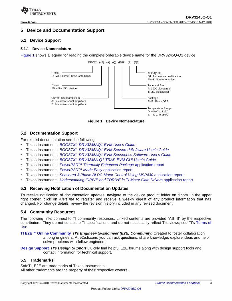
(R)(45)DRV32
PrefixDRV32: Three Phase Gate Driver
(A) (Q1)
Tape and Reel R: 3000 pieces/reel T: 250 pieces/reel
Series45: 4.5 ± 45 V device
(Q)
Current-shunt amplifiersA: 3x current-shunt amplifiersB: 2x current-shunt amplifiers
Temperature RangeQ: ±40°C to 125°CE: ±40°C to 150°C
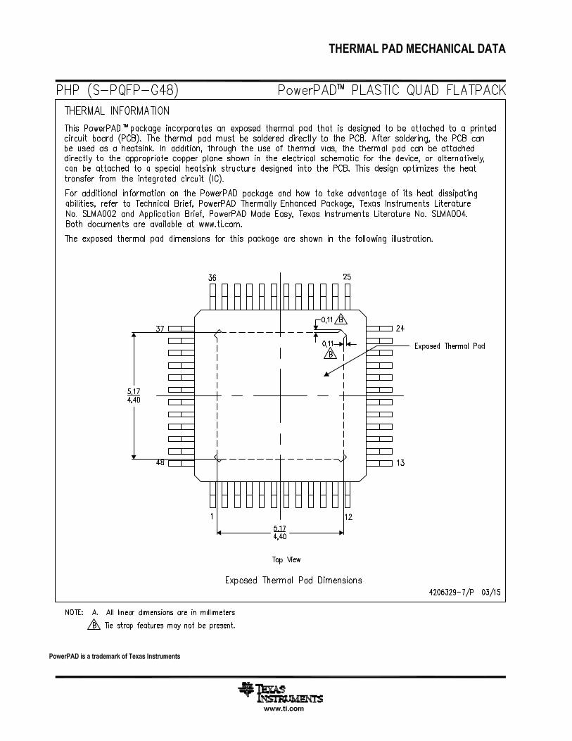
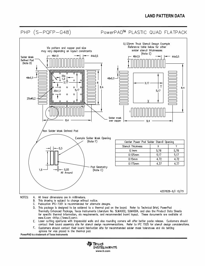
(PHP)
PackagePHP: 48-pin QFP
AEC-Q100 Q1: Automotive qualification Blank: Non-automotive
3
DRV3245Q-Q1www.ti.com SLVSEE3A –NOVEMBER 2017–REVISED MAY 2018
Product Folder Links: DRV3245Q-Q1
Submit Documentation FeedbackCopyright © 2017–2018, Texas Instruments Incorporated
5 Device and Documentation Support
5.1 Device Support
5.1.1 Device NomenclatureFigure 1 shows a legend for reading the complete orderable device name for the DRV3245Q-Q1 device
Figure 1. Device Nomenclature
5.2 Documentation SupportFor related documentation see the following:• Texas Instruments, BOOSTXL-DRV3245AQ1 EVM User's Guide• Texas Instruments, BOOSTXL-DRV3245AQ1 EVM Sensored Software User's Guide• Texas Instruments, BOOSTXL-DRV3245AQ1 EVM Sensorless Software User's Guide• Texas Instruments, BOOSTXL-DRV3245A-Q1 TRAP-EVM GUI User’s Guide• Texas Instruments, PowerPAD™ Thermally Enhanced Package application report• Texas Instruments, PowerPAD™ Made Easy application report• Texas Instruments, Sensored 3-Phase BLDC Motor Control Using MSP430 application report• Texas Instruments, Understanding IDRIVE and TDRIVE in TI Motor Gate Drivers application report
5.3 Receiving Notification of Documentation UpdatesTo receive notification of documentation updates, navigate to the device product folder on ti.com. In the upperright corner, click on Alert me to register and receive a weekly digest of any product information that haschanged. For change details, review the revision history included in any revised document.
5.4 Community ResourcesThe following links connect to TI community resources. Linked contents are provided "AS IS" by the respectivecontributors. They do not constitute TI specifications and do not necessarily reflect TI's views; see TI's Terms ofUse.
TI E2E™ Online Community TI's Engineer-to-Engineer (E2E) Community. Created to foster collaborationamong engineers. At e2e.ti.com, you can ask questions, share knowledge, explore ideas and helpsolve problems with fellow engineers.
Design Support TI's Design Support Quickly find helpful E2E forums along with design support tools andcontact information for technical support.
5.5 TrademarksSafeTI, E2E are trademarks of Texas Instruments.All other trademarks are the property of their respective owners.

4
DRV3245Q-Q1SLVSEE3A –NOVEMBER 2017–REVISED MAY 2018 www.ti.com
Product Folder Links: DRV3245Q-Q1
Submit Documentation Feedback Copyright © 2017–2018, Texas Instruments Incorporated
5.6 Electrostatic Discharge CautionThis integrated circuit can be damaged by ESD. Texas Instruments recommends that all integrated circuits be handled withappropriate precautions. Failure to observe proper handling and installation procedures can cause damage.
ESD damage can range from subtle performance degradation to complete device failure. Precision integrated circuits may be moresusceptible to damage because very small parametric changes could cause the device not to meet its published specifications.
5.7 GlossarySLYZ022 — TI Glossary.
This glossary lists and explains terms, acronyms, and definitions.
6 Mechanical, Packaging, and Orderable InformationThe following pages include mechanical, packaging, and orderable information. This information is the mostcurrent data available for the designated devices. This data is subject to change without notice and revision ofthis document. For browser-based versions of this data sheet, refer to the left-hand navigation.
PACKAGE OPTION ADDENDUM
www.ti.com 9-Jun-2018
Addendum-Page 1
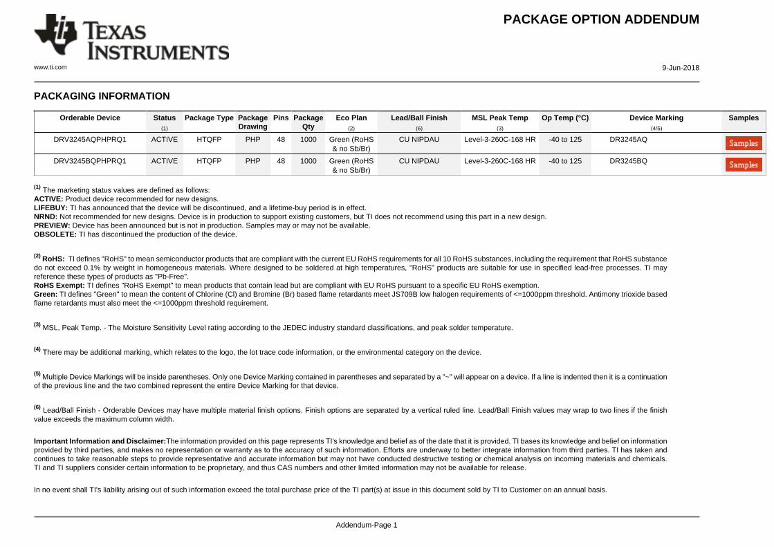
PACKAGING INFORMATION
Orderable Device Status(1)
Package Type PackageDrawing
Pins PackageQty
Eco Plan(2)
Lead/Ball Finish(6)
MSL Peak Temp(3)
Op Temp (°C) Device Marking(4/5)
Samples
DRV3245AQPHPRQ1 ACTIVE HTQFP PHP 48 1000 Green (RoHS& no Sb/Br)
CU NIPDAU Level-3-260C-168 HR -40 to 125 DR3245AQ
DRV3245BQPHPRQ1 ACTIVE HTQFP PHP 48 1000 Green (RoHS& no Sb/Br)
CU NIPDAU Level-3-260C-168 HR -40 to 125 DR3245BQ
(1) The marketing status values are defined as follows:ACTIVE: Product device recommended for new designs.LIFEBUY: TI has announced that the device will be discontinued, and a lifetime-buy period is in effect.NRND: Not recommended for new designs. Device is in production to support existing customers, but TI does not recommend using this part in a new design.PREVIEW: Device has been announced but is not in production. Samples may or may not be available.OBSOLETE: TI has discontinued the production of the device.
(2) RoHS: TI defines "RoHS" to mean semiconductor products that are compliant with the current EU RoHS requirements for all 10 RoHS substances, including the requirement that RoHS substancedo not exceed 0.1% by weight in homogeneous materials. Where designed to be soldered at high temperatures, "RoHS" products are suitable for use in specified lead-free processes. TI mayreference these types of products as "Pb-Free".RoHS Exempt: TI defines "RoHS Exempt" to mean products that contain lead but are compliant with EU RoHS pursuant to a specific EU RoHS exemption.Green: TI defines "Green" to mean the content of Chlorine (Cl) and Bromine (Br) based flame retardants meet JS709B low halogen requirements of <=1000ppm threshold. Antimony trioxide basedflame retardants must also meet the <=1000ppm threshold requirement.
(3) MSL, Peak Temp. - The Moisture Sensitivity Level rating according to the JEDEC industry standard classifications, and peak solder temperature.
(4) There may be additional marking, which relates to the logo, the lot trace code information, or the environmental category on the device.
(5) Multiple Device Markings will be inside parentheses. Only one Device Marking contained in parentheses and separated by a "~" will appear on a device. If a line is indented then it is a continuationof the previous line and the two combined represent the entire Device Marking for that device.
(6) Lead/Ball Finish - Orderable Devices may have multiple material finish options. Finish options are separated by a vertical ruled line. Lead/Ball Finish values may wrap to two lines if the finishvalue exceeds the maximum column width.
Important Information and Disclaimer:The information provided on this page represents TI's knowledge and belief as of the date that it is provided. TI bases its knowledge and belief on informationprovided by third parties, and makes no representation or warranty as to the accuracy of such information. Efforts are underway to better integrate information from third parties. TI has taken andcontinues to take reasonable steps to provide representative and accurate information but may not have conducted destructive testing or chemical analysis on incoming materials and chemicals.TI and TI suppliers consider certain information to be proprietary, and thus CAS numbers and other limited information may not be available for release.
In no event shall TI's liability arising out of such information exceed the total purchase price of the TI part(s) at issue in this document sold by TI to Customer on an annual basis.
PACKAGE OPTION ADDENDUM
www.ti.com 9-Jun-2018
Addendum-Page 2
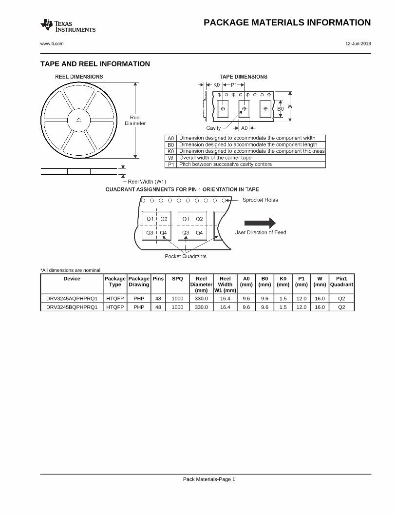
TAPE AND REEL INFORMATION
*All dimensions are nominal
Device PackageType
PackageDrawing
Pins SPQ ReelDiameter
(mm)
ReelWidth
W1 (mm)
A0(mm)
B0(mm)
K0(mm)
P1(mm)
W(mm)
Pin1Quadrant
DRV3245AQPHPRQ1 HTQFP PHP 48 1000 330.0 16.4 9.6 9.6 1.5 12.0 16.0 Q2
DRV3245BQPHPRQ1 HTQFP PHP 48 1000 330.0 16.4 9.6 9.6 1.5 12.0 16.0 Q2
PACKAGE MATERIALS INFORMATION
www.ti.com 12-Jun-2018
Pack Materials-Page 1
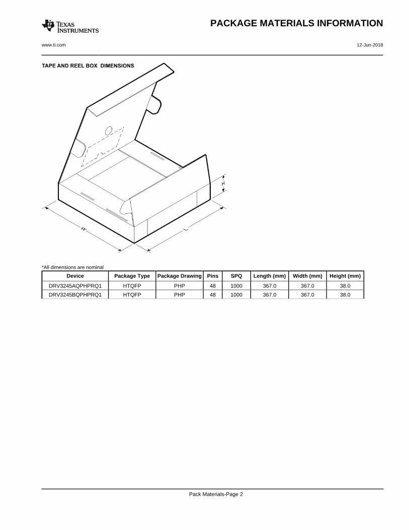
*All dimensions are nominal
Device Package Type Package Drawing Pins SPQ Length (mm) Width (mm) Height (mm)
DRV3245AQPHPRQ1 HTQFP PHP 48 1000 367.0 367.0 38.0
DRV3245BQPHPRQ1 HTQFP PHP 48 1000 367.0 367.0 38.0
PACKAGE MATERIALS INFORMATION
www.ti.com 12-Jun-2018
Pack Materials-Page 2
IMPORTANT NOTICE
Texas Instruments Incorporated (TI) reserves the right to make corrections, enhancements, improvements and other changes to itssemiconductor products and services per JESD46, latest issue, and to discontinue any product or service per JESD48, latest issue. Buyersshould obtain the latest relevant information before placing orders and should verify that such information is current and complete.TI’s published terms of sale for semiconductor products (http://www.ti.com/sc/docs/stdterms.htm) apply to the sale of packaged integratedcircuit products that TI has qualified and released to market. Additional terms may apply to the use or sale of other types of TI products andservices.Reproduction of significant portions of TI information in TI data sheets is permissible only if reproduction is without alteration and isaccompanied by all associated warranties, conditions, limitations, and notices. TI is not responsible or liable for such reproduceddocumentation. Information of third parties may be subject to additional restrictions. Resale of TI products or services with statementsdifferent from or beyond the parameters stated by TI for that product or service voids all express and any implied warranties for theassociated TI product or service and is an unfair and deceptive business practice. TI is not responsible or liable for any such statements.Buyers and others who are developing systems that incorporate TI products (collectively, “Designers”) understand and agree that Designersremain responsible for using their independent analysis, evaluation and judgment in designing their applications and that Designers havefull and exclusive responsibility to assure the safety of Designers' applications and compliance of their applications (and of all TI productsused in or for Designers’ applications) with all applicable regulations, laws and other applicable requirements. Designer represents that, withrespect to their applications, Designer has all the necessary expertise to create and implement safeguards that (1) anticipate dangerousconsequences of failures, (2) monitor failures and their consequences, and (3) lessen the likelihood of failures that might cause harm andtake appropriate actions. Designer agrees that prior to using or distributing any applications that include TI products, Designer willthoroughly test such applications and the functionality of such TI products as used in such applications.TI’s provision of technical, application or other design advice, quality characterization, reliability data or other services or information,including, but not limited to, reference designs and materials relating to evaluation modules, (collectively, “TI Resources”) are intended toassist designers who are developing applications that incorporate TI products; by downloading, accessing or using TI Resources in anyway, Designer (individually or, if Designer is acting on behalf of a company, Designer’s company) agrees to use any particular TI Resourcesolely for this purpose and subject to the terms of this Notice.TI’s provision of TI Resources does not expand or otherwise alter TI’s applicable published warranties or warranty disclaimers for TIproducts, and no additional obligations or liabilities arise from TI providing such TI Resources. TI reserves the right to make corrections,enhancements, improvements and other changes to its TI Resources. TI has not conducted any testing other than that specificallydescribed in the published documentation for a particular TI Resource.Designer is authorized to use, copy and modify any individual TI Resource only in connection with the development of applications thatinclude the TI product(s) identified in such TI Resource. NO OTHER LICENSE, EXPRESS OR IMPLIED, BY ESTOPPEL OR OTHERWISETO ANY OTHER TI INTELLECTUAL PROPERTY RIGHT, AND NO LICENSE TO ANY TECHNOLOGY OR INTELLECTUAL PROPERTYRIGHT OF TI OR ANY THIRD PARTY IS GRANTED HEREIN, including but not limited to any patent right, copyright, mask work right, orother intellectual property right relating to any combination, machine, or process in which TI products or services are used. Informationregarding or referencing third-party products or services does not constitute a license to use such products or services, or a warranty orendorsement thereof. Use of TI Resources may require a license from a third party under the patents or other intellectual property of thethird party, or a license from TI under the patents or other intellectual property of TI.TI RESOURCES ARE PROVIDED “AS IS” AND WITH ALL FAULTS. TI DISCLAIMS ALL OTHER WARRANTIES ORREPRESENTATIONS, EXPRESS OR IMPLIED, REGARDING RESOURCES OR USE THEREOF, INCLUDING BUT NOT LIMITED TOACCURACY OR COMPLETENESS, TITLE, ANY EPIDEMIC FAILURE WARRANTY AND ANY IMPLIED WARRANTIES OFMERCHANTABILITY, FITNESS FOR A PARTICULAR PURPOSE, AND NON-INFRINGEMENT OF ANY THIRD PARTY INTELLECTUALPROPERTY RIGHTS. TI SHALL NOT BE LIABLE FOR AND SHALL NOT DEFEND OR INDEMNIFY DESIGNER AGAINST ANY CLAIM,INCLUDING BUT NOT LIMITED TO ANY INFRINGEMENT CLAIM THAT RELATES TO OR IS BASED ON ANY COMBINATION OFPRODUCTS EVEN IF DESCRIBED IN TI RESOURCES OR OTHERWISE. IN NO EVENT SHALL TI BE LIABLE FOR ANY ACTUAL,DIRECT, SPECIAL, COLLATERAL, INDIRECT, PUNITIVE, INCIDENTAL, CONSEQUENTIAL OR EXEMPLARY DAMAGES INCONNECTION WITH OR ARISING OUT OF TI RESOURCES OR USE THEREOF, AND REGARDLESS OF WHETHER TI HAS BEENADVISED OF THE POSSIBILITY OF SUCH DAMAGES.Unless TI has explicitly designated an individual product as meeting the requirements of a particular industry standard (e.g., ISO/TS 16949and ISO 26262), TI is not responsible for any failure to meet such industry standard requirements.Where TI specifically promotes products as facilitating functional safety or as compliant with industry functional safety standards, suchproducts are intended to help enable customers to design and create their own applications that meet applicable functional safety standardsand requirements. Using products in an application does not by itself establish any safety features in the application. Designers mustensure compliance with safety-related requirements and standards applicable to their applications. Designer may not use any TI products inlife-critical medical equipment unless authorized officers of the parties have executed a special contract specifically governing such use.Life-critical medical equipment is medical equipment where failure of such equipment would cause serious bodily injury or death (e.g., lifesupport, pacemakers, defibrillators, heart pumps, neurostimulators, and implantables). Such equipment includes, without limitation, allmedical devices identified by the U.S. Food and Drug Administration as Class III devices and equivalent classifications outside the U.S.TI may expressly designate certain products as completing a particular qualification (e.g., Q100, Military Grade, or Enhanced Product).Designers agree that it has the necessary expertise to select the product with the appropriate qualification designation for their applicationsand that proper product selection is at Designers’ own risk. Designers are solely responsible for compliance with all legal and regulatoryrequirements in connection with such selection.Designer will fully indemnify TI and its representatives against any damages, costs, losses, and/or liabilities arising out of Designer’s non-compliance with the terms and provisions of this Notice.
Mailing Address: Texas Instruments, Post Office Box 655303, Dallas, Texas 75265Copyright © 2018, Texas Instruments Incorporated