Document Number: MRF6V4300N Technical Data Rev. 3, 4/2010...
15
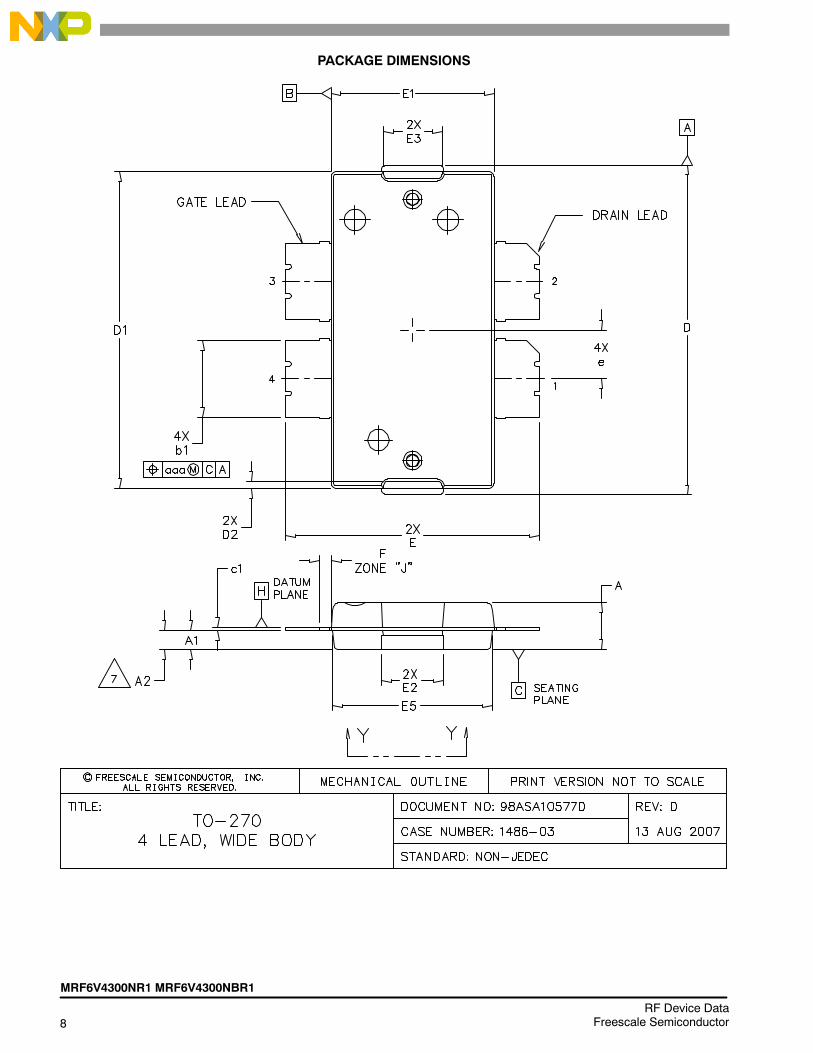
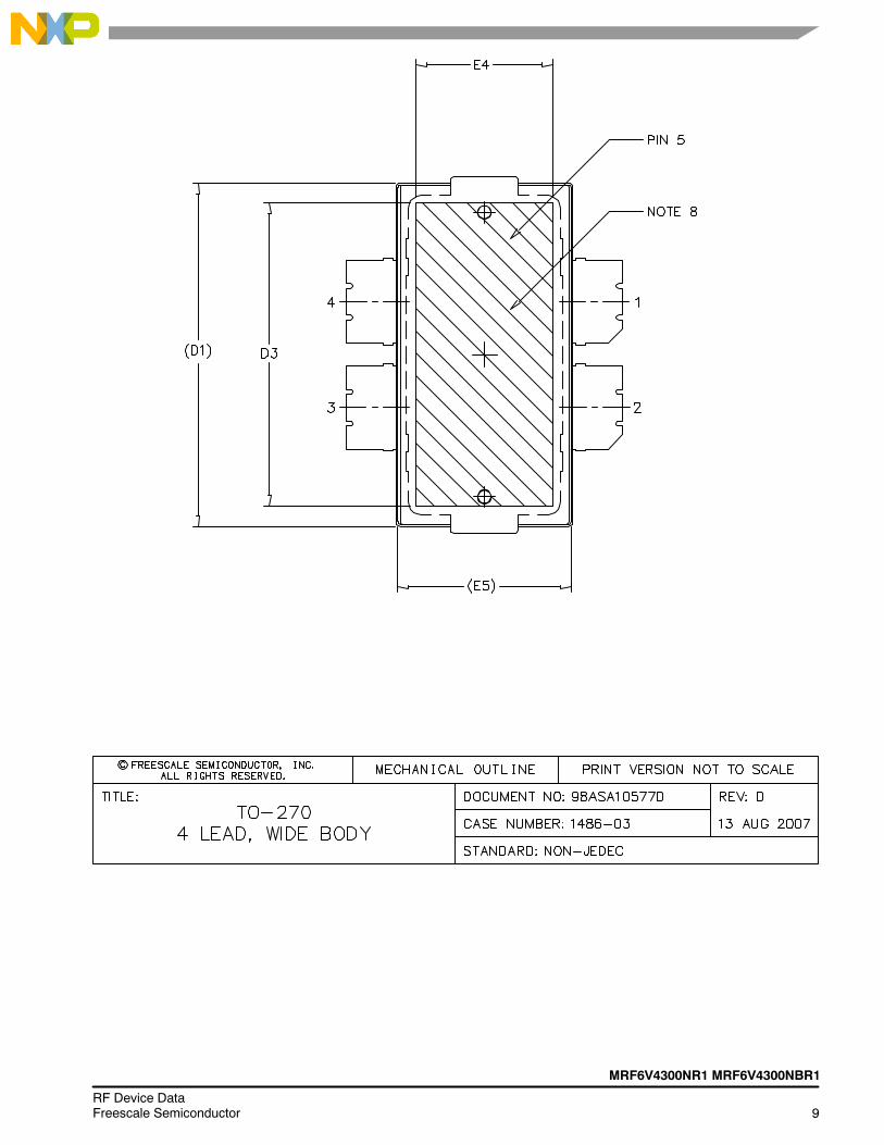
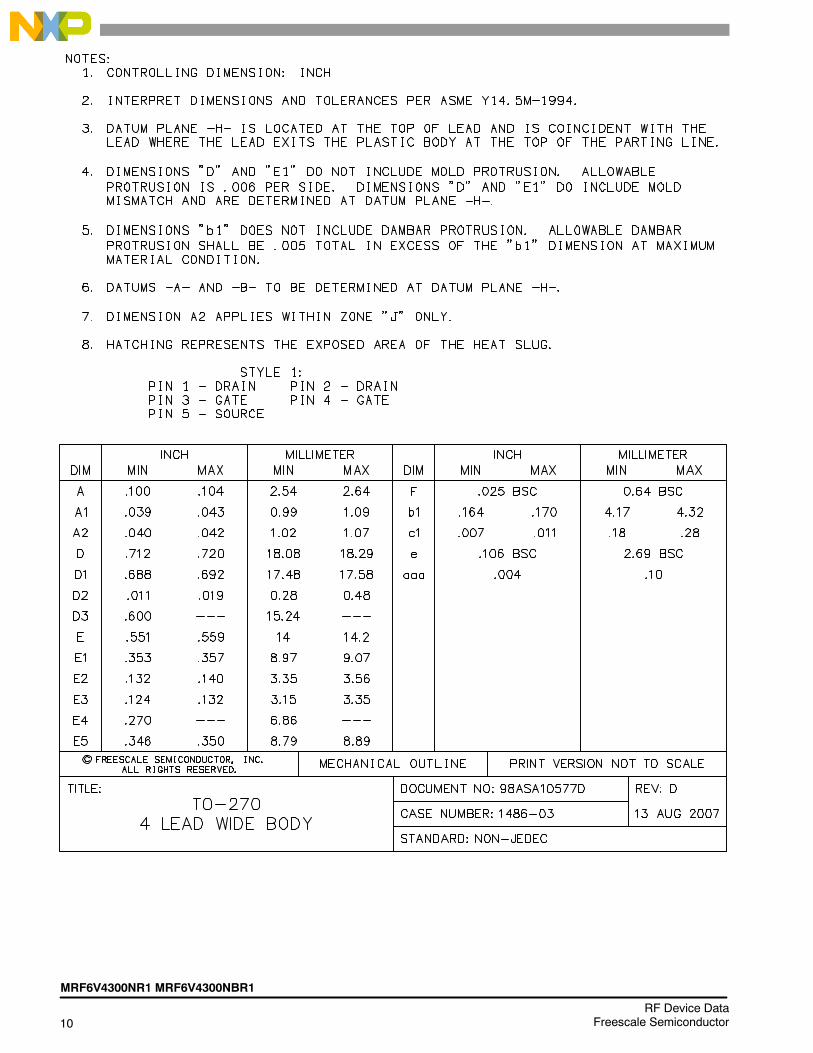
RF Power Field Effect Transistors N--Channel Enhancement--Mode Lateral MOSFETs Designed primarily for CW large--signal output and driver applications with frequencies up to 600 MHz. Devices are unmatched and are suitable for use in industrial, medical and scientific applications. • Typical CW Performance: V DD = 50 Volts, I DQ = 900 mA, P out = 300 Watts, f = 450 MHz Power Gain 22 dB Drain Efficiency 60% • Capable of Handling 10:1 VSWR, @ 50 Vdc, 450 MHz, 300 Watts CW Output Power Features • Characterized with Series Equivalent Large--Signal Impedance Parameters • Qualified Up to a Maximum of 50 V DD Operation • Integrated ESD Protection • Greater Negative Gate--Source Voltage Range for Improved Class C Operation • 225°C Capable Plastic Package • RoHS Compliant • In Tape and Reel. R1 Suffix = 500 Units per 44 mm, 13 inch Reel. Table 1. Maximum Ratings Rating Symbol Value Unit Drain--Source Voltage V DSS --0.5, +110 Vdc Gate--Source Voltage V GS --6.0, +10 Vdc Storage Temperature Range T stg --65 to +150 °C Case Operating Temperature T C 150 °C Operating Junction Temperature (1,2) T J 225 °C 1. Continuous use at maximum temperature will affect MTTF. 2. MTTF calculator available at http://www.freescale.com/rf . Select Software & Tools/Development Tools/Calculators to access MTTF calculators by product. Document Number: MRF6V4300N Rev. 3, 4/2010 Freescale Semiconductor Technical Data MRF6V4300NR1 MRF6V4300NBR1 CASE 1484--04, STYLE 1 TO--272 WB--4 PLASTIC MRF6V4300NBR1 CASE 1486--03, STYLE 1 TO--270 WB--4 PLASTIC MRF6V4300NR1 10--600 MHz, 300 W, 50 V LATERAL N--CHANNEL SINGLE--ENDED BROADBAND RF POWER MOSFETs PARTS ARE SINGLE--ENDED (Top View) RF out /V DS Figure 1. Pin Connections RF out /V DS RF in /V GS RF in /V GS Note: Exposed backside of the package is the source terminal for the transistor. © Freescale Semiconductor, Inc., 2008--2010. All rights reserved.
Transcript of Document Number: MRF6V4300N Technical Data Rev. 3, 4/2010...

MRF6V4300NR1 MRF6V4300NBR1
1RF Device DataFreescale Semiconductor
RF Power Field Effect TransistorsN--Channel Enhancement--Mode Lateral MOSFETsDesigned primarily for CW large--signal output and driver applications with
frequencies up to 600 MHz. Devices are unmatched and are suitable for use inindustrial, medical and scientific applications.
• Typical CW Performance: VDD = 50 Volts, IDQ = 900 mA, Pout = 300 Watts,f = 450 MHzPower Gain 22 dBDrain Efficiency 60%
• Capable of Handling 10:1 VSWR, @ 50 Vdc, 450 MHz, 300 Watts CWOutput Power
Features• Characterized with Series Equivalent Large--Signal Impedance Parameters
• Qualified Up to a Maximum of 50 VDD Operation
• Integrated ESD Protection
• Greater Negative Gate--Source Voltage Range for Improved Class COperation
• 225°C Capable Plastic Package
• RoHS Compliant
• In Tape and Reel. R1 Suffix = 500 Units per 44 mm, 13 inch Reel.
Table 1. Maximum Ratings
Rating Symbol Value Unit
Drain--Source Voltage VDSS --0.5, +110 Vdc
Gate--Source Voltage VGS --6.0, +10 Vdc
Storage Temperature Range Tstg -- 65 to +150 °C
Case Operating Temperature TC 150 °C
Operating Junction Temperature (1,2) TJ 225 °C
1. Continuous use at maximum temperature will affect MTTF.2. MTTF calculator available at http://www.freescale.com/rf. Select Software & Tools/Development Tools/Calculators to access
MTTF calculators by product.
Document Number: MRF6V4300NRev. 3, 4/2010
Freescale SemiconductorTechnical Data
MRF6V4300NR1MRF6V4300NBR1
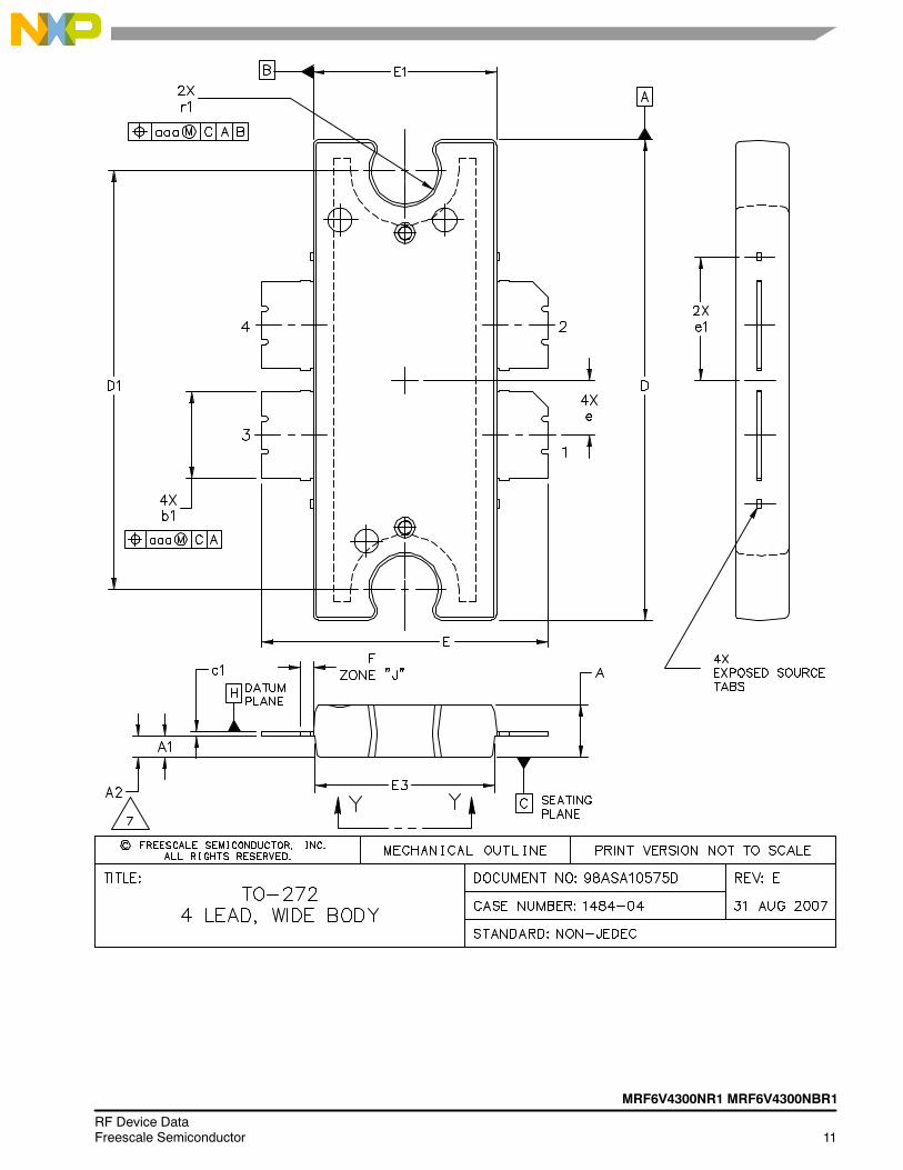
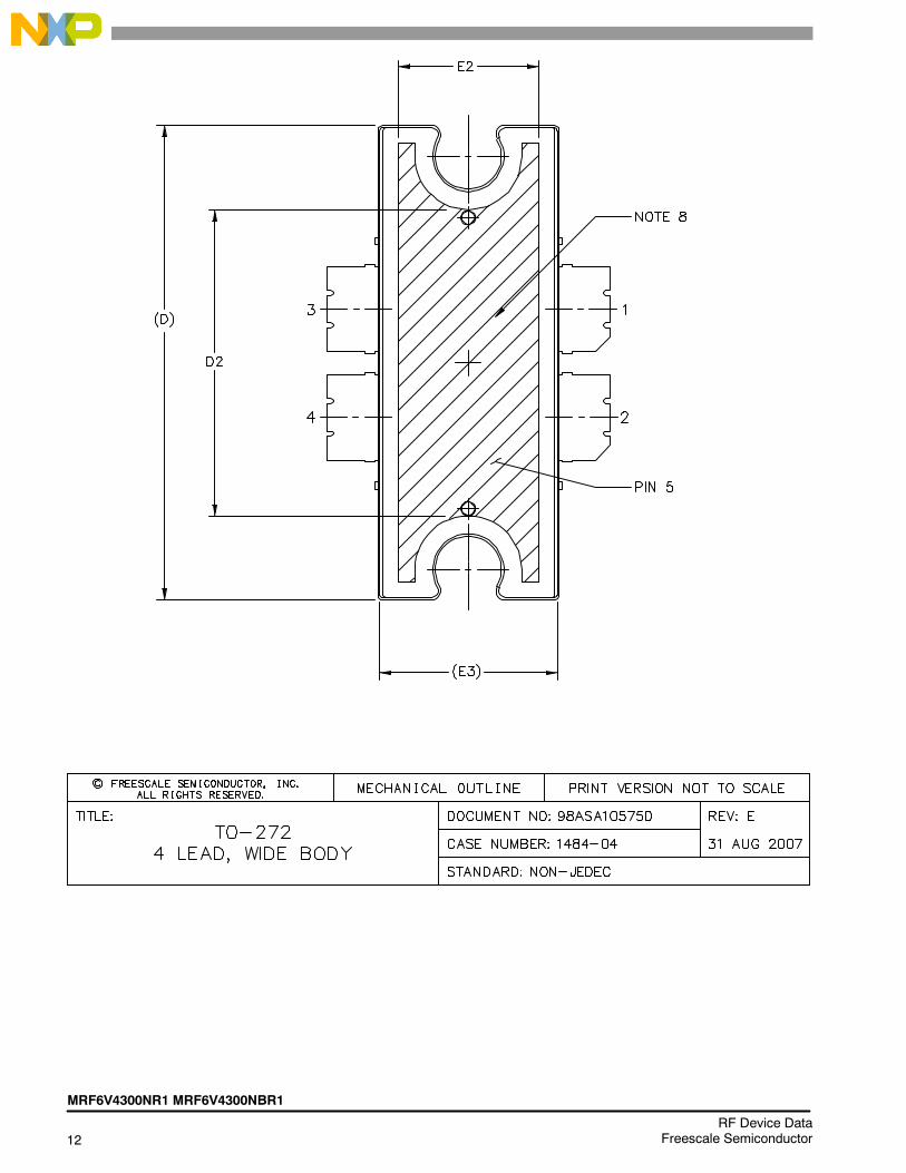
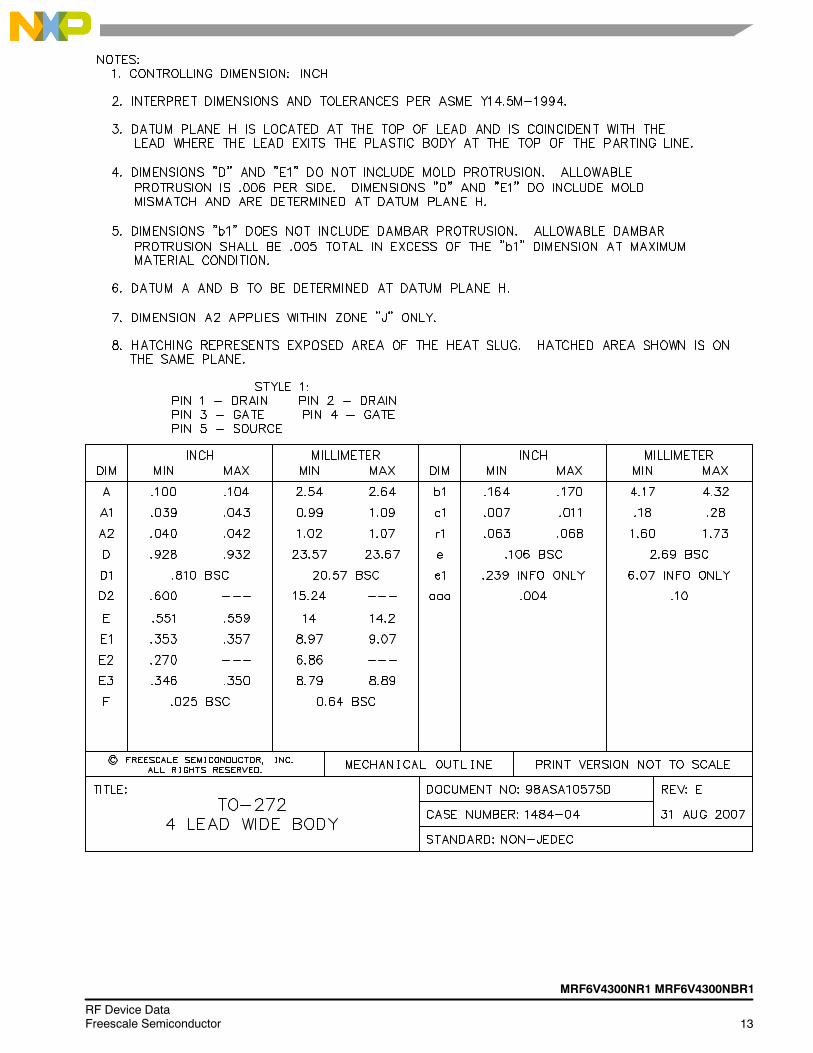
CASE 1484--04, STYLE 1TO--272 WB--4PLASTIC
MRF6V4300NBR1
CASE 1486--03, STYLE 1TO--270 WB--4PLASTIC
MRF6V4300NR1
10--600 MHz, 300 W, 50 VLATERAL N--CHANNEL
SINGLE--ENDEDBROADBAND
RF POWER MOSFETs
PARTS ARE SINGLE--ENDED
(Top View)
RFout/VDS
Figure 1. Pin Connections
RFout/VDS
RFin/VGS
RFin/VGS
Note: Exposed backside of the package isthe source terminal for the transistor.
© Freescale Semiconductor, Inc., 2008--2010. All rights reserved.
2RF Device Data
Freescale Semiconductor
MRF6V4300NR1 MRF6V4300NBR1
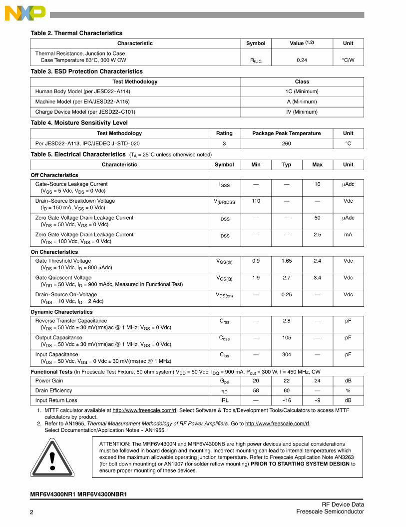
Table 2. Thermal Characteristics
Characteristic Symbol Value (1,2) Unit
Thermal Resistance, Junction to CaseCase Temperature 83°C, 300 W CW RθJC 0.24 °C/W
Table 3. ESD Protection Characteristics
Test Methodology Class
Human Body Model (per JESD22--A114) 1C (Minimum)
Machine Model (per EIA/JESD22--A115) A (Minimum)
Charge Device Model (per JESD22--C101) IV (Minimum)
Table 4. Moisture Sensitivity Level
Test Methodology Rating Package Peak Temperature Unit
Per JESD22--A113, IPC/JEDEC J--STD--020 3 260 °C
Table 5. Electrical Characteristics (TA = 25°C unless otherwise noted)
Characteristic Symbol Min Typ Max Unit
Off Characteristics
Gate--Source Leakage Current(VGS = 5 Vdc, VDS = 0 Vdc)
IGSS 10 μAdc
Drain--Source Breakdown Voltage(ID = 150 mA, VGS = 0 Vdc)
V(BR)DSS 110 Vdc
Zero Gate Voltage Drain Leakage Current(VDS = 50 Vdc, VGS = 0 Vdc)
IDSS 50 μAdc
Zero Gate Voltage Drain Leakage Current(VDS = 100 Vdc, VGS = 0 Vdc)
IDSS 2.5 mA
On Characteristics
Gate Threshold Voltage(VDS = 10 Vdc, ID = 800 μAdc)
VGS(th) 0.9 1.65 2.4 Vdc
Gate Quiescent Voltage(VDD = 50 Vdc, ID = 900 mAdc, Measured in Functional Test)
VGS(Q) 1.9 2.7 3.4 Vdc
Drain--Source On--Voltage(VGS = 10 Vdc, ID = 2 Adc)
VDS(on) 0.25 Vdc
Dynamic Characteristics
Reverse Transfer Capacitance(VDS = 50 Vdc ± 30 mV(rms)ac @ 1 MHz, VGS = 0 Vdc)
Crss 2.8 pF
Output Capacitance(VDS = 50 Vdc ± 30 mV(rms)ac @ 1 MHz, VGS = 0 Vdc)
Coss 105 pF
Input Capacitance(VDS = 50 Vdc, VGS = 0 Vdc ± 30 mV(rms)ac @ 1 MHz)
Ciss 304 pF
Functional Tests (In Freescale Test Fixture, 50 ohm system) VDD = 50 Vdc, IDQ = 900 mA, Pout = 300 W, f = 450 MHz, CW
Power Gain Gps 20 22 24 dB
Drain Efficiency ηD 58 60 %
Input Return Loss IRL --16 --9 dB
1. MTTF calculator available at http://www.freescale.com/rf. Select Software & Tools/Development Tools/Calculators to access MTTFcalculators by product.
2. Refer to AN1955, Thermal Measurement Methodology of RF Power Amplifiers. Go to http://www.freescale.com/rf.Select Documentation/Application Notes -- AN1955.
ATTENTION: The MRF6V4300N and MRF6V4300NB are high power devices and special considerationsmust be followed in board design and mounting. Incorrect mounting can lead to internal temperatures whichexceed the maximum allowable operating junction temperature. Refer to Freescale Application Note AN3263(for bolt down mounting) or AN1907 (for solder reflow mounting) PRIOR TO STARTING SYSTEM DESIGN toensure proper mounting of these devices.
MRF6V4300NR1 MRF6V4300NBR1
3RF Device DataFreescale Semiconductor
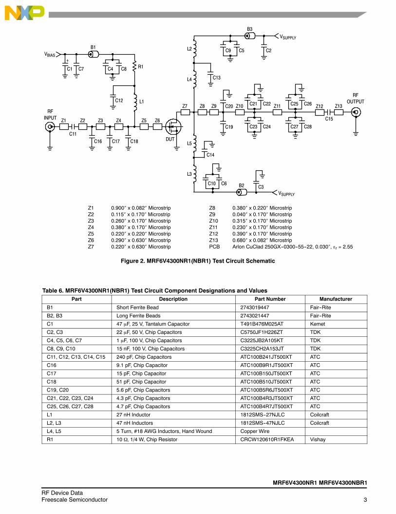
Figure 2. MRF6V4300NR1(NBR1) Test Circuit Schematic
Z8 0.380″ x 0.220″ MicrostripZ9 0.040″ x 0.170″ MicrostripZ10 0.315″ x 0.170″ MicrostripZ11 0.230″ x 0.170″ MicrostripZ12 0.390″ x 0.170″ MicrostripZ13 0.680″ x 0.082″ MicrostripPCB Arlon CuClad 250GX--0300--55--22, 0.030″, εr = 2.55
Z1 0.900″ x 0.082″ MicrostripZ2 0.115″ x 0.170″ MicrostripZ3 0.260″ x 0.170″ MicrostripZ4 0.380″ x 0.170″ MicrostripZ5 0.220″ x 0.220″ MicrostripZ6 0.290″ x 0.630″ MicrostripZ7 0.220″ x 0.630″ Microstrip
Z1
RFINPUT
C11
Z2 Z3 Z4 Z5 Z6
DUT
Z9
C15
RFOUTPUT
Z10
C4
B1VBIAS
VSUPPLY
C7 R1
C2
C1
+
C8
Z7 Z13Z8
B3
C19
L1C12
C16
L4
L2
C13
C17 C18
C9 C5
C21 C22C20
C23 C24
Z12C25 C26
C27 C28
Z11
L3
L5
C14
C10 C6 B2 C3VSUPPLY
Table 6. MRF6V4300NR1(NBR1) Test Circuit Component Designations and ValuesPart Description Part Number Manufacturer
B1 Short Ferrite Bead 2743019447 Fair--Rite
B2, B3 Long Ferrite Beads 2743021447 Fair--Rite
C1 47 μF, 25 V, Tantalum Capacitor T491B476M025AT Kemet
C2, C3 22 μF, 50 V, Chip Capacitors C5750JF1H226ZT TDK
C4, C5, C6, C7 1 μF, 100 V, Chip Capacitors C3225JB2A105KT TDK
C8, C9, C10 15 nF, 100 V, Chip Capacitors C3225CH2A153JT TDK
C11, C12, C13, C14, C15 240 pF, Chip Capacitors ATC100B241JT500XT ATC
C16 9.1 pF, Chip Capacitor ATC100B9R1JT500XT ATC
C17 15 pF, Chip Capacitor ATC100B150JT500XT ATC
C18 51 pF, Chip Capacitor ATC100B510JT500XT ATC
C19, C20 5.6 pF, Chip Capacitors ATC100B5R6JT500XT ATC
C21, C22, C23, C24 4.3 pF, Chip Capacitors ATC100B4R3JT500XT ATC
C25, C26, C27, C28 4.7 pF, Chip Capacitors ATC100B4R7JT500XT ATC
L1 27 nH Inductor 1812SMS--27NJLC Coilcraft
L2, L3 47 nH Inductors 1812SMS--47NJLC Coilcraft
L4, L5 5 Turn, #18 AWG Inductors, Hand Wound Copper Wire
R1 10 Ω, 1/4 W, Chip Resistor CRCW120610R1FKEA Vishay
4RF Device Data
Freescale Semiconductor
MRF6V4300NR1 MRF6V4300NBR1
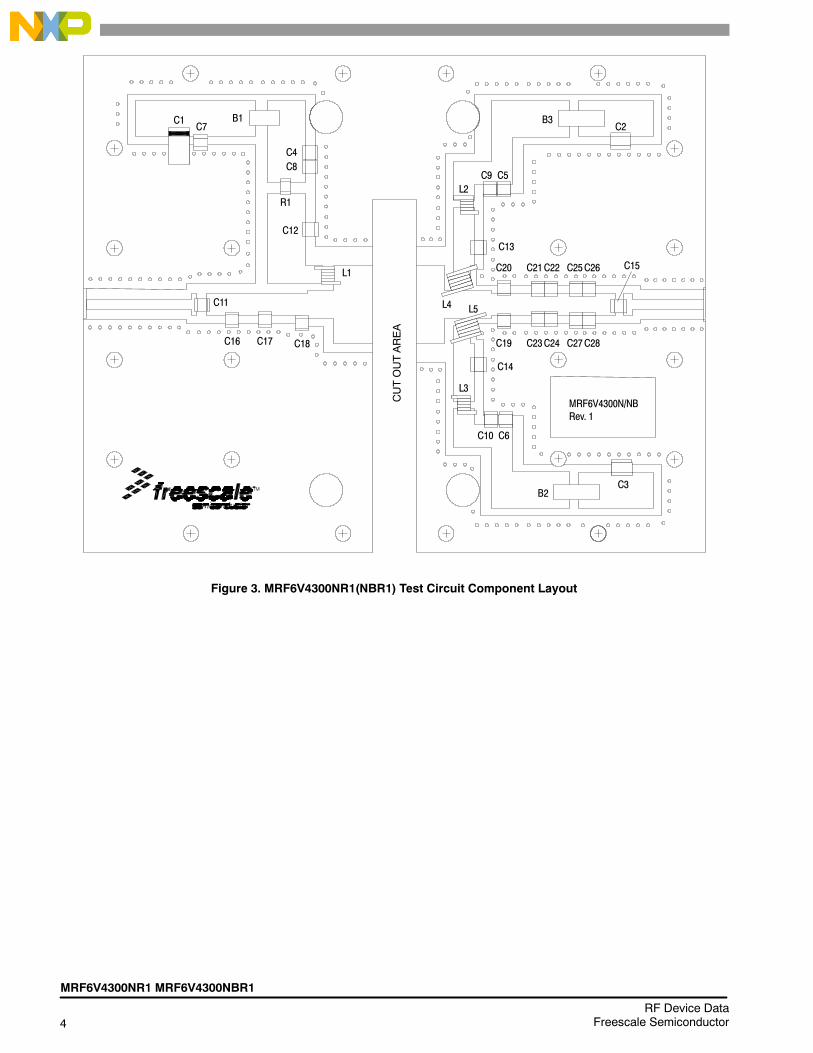
Figure 3. MRF6V4300NR1(NBR1) Test Circuit Component Layout
ATC
MRF6V4300N/NBCUTOUTAREA
Rev. 1
C1C7
B1
R1
C4C8
C12
L1
C11
C16 C17 C18
B3C2
C9 C5L2
C13
L4 L5
C20 C21C22 C25C26
C19 C23C24 C27C28
C15
L3
C14
C10 C6
B2C3

MRF6V4300NR1 MRF6V4300NBR1
5RF Device DataFreescale Semiconductor
TYPICAL CHARACTERISTICS
501
1000
0 2010
VDS, DRAIN--SOURCE VOLTAGE (VOLTS)
Figure 4. Capacitance versus Drain--Source Voltage
C,CAPACITANCE(pF)
30
Ciss
1
100
1
TC = 25°C
10
10
VDS, DRAIN--SOURCE VOLTAGE (VOLTS)
Figure 5. DC Safe Operating Area
I D,DRAINCURRENT(AMPS)
400
10
0
DRAIN VOLTAGE (VOLTS)
9
8
7
6
20 120
Figure 6. DC Drain Current versus Drain Voltage
I D,DRAINCURRENT(AMPS)
60 60018
23
IDQ = 1350 mA
10
22
21
20
Pout, OUTPUT POWER (WATTS) CW
Figure 7. CW Power Gain versus Output Power
Gps,POWER
GAIN(dB)
VDD = 50 Vdcf = 450 MHz
100
10
40 100
5
VGS = 3 V
Coss
Crss
80 100
4
3
2
1
2.75 V
2.63 V
2.5 V
2.25 V
19
100
1125 mA900 mA
450 mA
100
--55
--15
10
Pout, OUTPUT POWER (WATTS) PEP
--25--30
--35
--40
600
Figure 8. Third Order Intermodulation Distortionversus Output Power
IMD,THIRDORDER
INTERMODULATION
DISTORTION(dBc)
VDD = 50 Vdc, f1 = 450 MHz, f2 = 450.1 MHzTwo--Tone Measurements, 100 kHz Tone Spacing
--45--50
--20
IDQ = 450 mA
1350 mA
900 mA
650 mA
1125 mA
3850
60
28 3129
58
56
54
52
Pin, INPUT POWER (dBm)
Figure 9. CW Output Power versus Input Power
P out,OUTPUTPOWER
(dBm
)
30 34
P3dB = 56.06 dBm (403 W)
Actual
Ideal
P1dB = 55.15 dBm (327 W)
VDD = 50 Vdc, IDQ = 900 mAf = 450 MHz
Measured with ±30 mV(rms)ac @ 1 MHzVGS = 0 Vdc
650 mA
--60
--10
--5
0
59
57
55
53
51
3332 35 36 37
6RF Device Data
Freescale Semiconductor
MRF6V4300NR1 MRF6V4300NBR1
TYPICAL CHARACTERISTICS
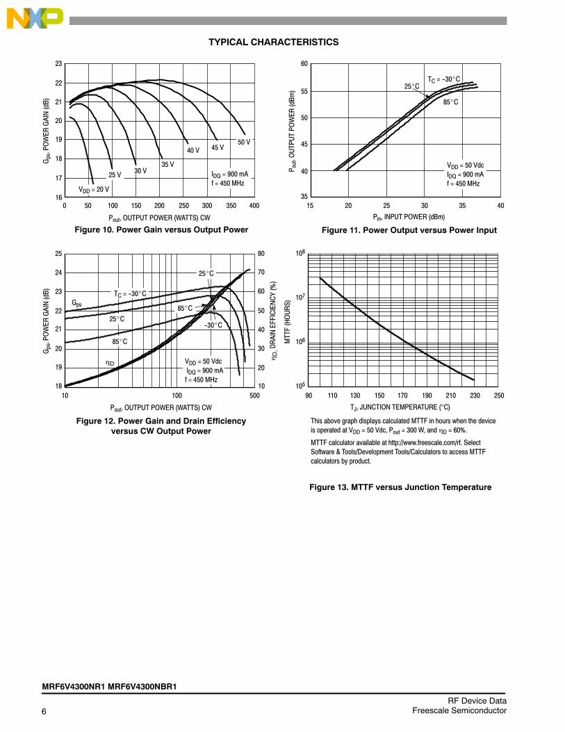
Figure 10. Power Gain versus Output PowerPout, OUTPUT POWER (WATTS) CW
Gps,POWER
GAIN(dB)
VDD = 20 V
25 V
40016
23
0 20050
18
17
100 150
21
20
22
IDQ = 900 mAf = 450 MHz
35 V
40 V
19
250 300 350
45 V
4035
60
15
25_CTC = --30_C
85_C
25
50
45
40
Pin, INPUT POWER (dBm)
Figure 11. Power Output versus Power Input
P out,OUTPUTPOWER
(dBm
)
VDD = 50 VdcIDQ = 900 mAf = 450 MHz
20 30
55
18
25
1010
80
24
22
20
70
60
50
40
30
20
Pout, OUTPUT POWER (WATTS) CW
Figure 12. Power Gain and Drain Efficiencyversus CW Output Power
Gps,POWER
GAIN(dB)
ηD,DRAINEFFICIENCY(%)
ηD
23
21
19
100 500
25_C
TC = --30_C
85_C
85_CGps
VDD = 50 VdcIDQ = 900 mAf = 450 MHz
25_C
--30_C
30 V
50 V
35
25090
TJ, JUNCTION TEMPERATURE (°C)
Figure 13. MTTF versus Junction Temperature
This above graph displays calculated MTTF in hours when the deviceis operated at VDD = 50 Vdc, Pout = 300 W, and ηD = 60%.
MTTF calculator available at http://www.freescale.com/rf. SelectSoftware & Tools/Development Tools/Calculators to access MTTFcalculators by product.
108
107
105
110 130 150 170 190
MTTF(HOURS)
210 230
106

MRF6V4300NR1 MRF6V4300NBR1
7RF Device DataFreescale Semiconductor
Zo = 2Ω
Zload
Zsource
f = 450 MHz
f = 450 MHz
VDD = 50 Vdc, IDQ = 900 mA, Pout = 300 W CW
fMHz
ZsourceΩ
ZloadΩ
450 0.39 + j1.26 1.27 + j0.96
Zsource = Test circuit impedance as measured fromgate to ground.
Zload = Test circuit impedance as measured fromdrain to ground.
Figure 14. Series Equivalent Source and Load Impedance
Zsource Z load
InputMatchingNetwork
DeviceUnderTest
OutputMatchingNetwork
8RF Device Data
Freescale Semiconductor
MRF6V4300NR1 MRF6V4300NBR1
PACKAGE DIMENSIONS
MRF6V4300NR1 MRF6V4300NBR1
9RF Device DataFreescale Semiconductor
10RF Device Data
Freescale Semiconductor
MRF6V4300NR1 MRF6V4300NBR1
MRF6V4300NR1 MRF6V4300NBR1
11RF Device DataFreescale Semiconductor
12RF Device Data
Freescale Semiconductor
MRF6V4300NR1 MRF6V4300NBR1
MRF6V4300NR1 MRF6V4300NBR1
13RF Device DataFreescale Semiconductor

14RF Device Data
Freescale Semiconductor
MRF6V4300NR1 MRF6V4300NBR1
PRODUCT DOCUMENTATION AND SOFTWARE
Refer to the following documents to aid your design process.
Application Notes• AN1907: Solder Reflow Attach Method for High Power RF Devices in Plastic Packages
• AN1955: Thermal Measurement Methodology of RF Power Amplifiers
• AN3263: Bolt Down Mounting Method for High Power RF Transistors and RFICs in Over--Molded Plastic Packages
• AN3789: Clamping of High Power RF Transistors and RFICs in Over--Molded Plastic Packages
Engineering Bulletins• EB212: Using Data Sheet Impedances for RF LDMOS Devices
Software• Electromigration MTTF Calculator• RF High Power Model
For Software, do a Part Number search at http://www.freescale.com, and select the Part Number link. Go to the Software &Tools tab on the parts Product Summary page to download the respective tool.
REVISION HISTORY
The following table summarizes revisions to this document.
Revision Date Description
0 July 2008 • Initial Release of Data Sheet
1 Oct. 2008 • Added Fig. 13, MTTF versus Junction Temperature, p. 6
2 Mar. 2009 • Corrected Zsource, 0.40 + j5.93 to 0.39 + j1.26 and Zload, 1.42 + j5.5 to 1.27 + j0.96 in Fig. 14, SeriesEquivalent Source and Load Impedance data table and replotted data, p. 7
3 Apr. 2010 • Operating Junction Temperature increased from 200°C to 225°C in Maximum Ratings table, relatedContinuous use at maximum temperature will affect MTTF footnote added and changed 200°C to 225°Cin Capable Plastic Package bullet, p. 1
• Added Electromigration MTTF Calculator and RF High Power Model availability to Product Software,p. 14
MRF6V4300NR1 MRF6V4300NBR1
15RF Device DataFreescale Semiconductor
Information in this document is provided solely to enable system and softwareimplementers to use Freescale Semiconductor products. There are no express orimplied copyright licenses granted hereunder to design or fabricate any integratedcircuits or integrated circuits based on the information in this document.
Freescale Semiconductor reserves the right to make changes without further notice toany products herein. Freescale Semiconductor makes no warranty, representation orguarantee regarding the suitability of its products for any particular purpose, nor doesFreescale Semiconductor assume any liability arising out of the application or use ofany product or circuit, and specifically disclaims any and all liability, including withoutlimitation consequential or incidental damages. Typical parameters that may beprovided in Freescale Semiconductor data sheets and/or specifications can and dovary in different applications and actual performance may vary over time. All operatingparameters, including Typicals, must be validated for each customer application bycustomers technical experts. Freescale Semiconductor does not convey any licenseunder its patent rights nor the rights of others. Freescale Semiconductor products arenot designed, intended, or authorized for use as components in systems intended forsurgical implant into the body, or other applications intended to support or sustain life,or for any other application in which the failure of the Freescale Semiconductor productcould create a situation where personal injury or death may occur. Should Buyerpurchase or use Freescale Semiconductor products for any such unintended orunauthorized application, Buyer shall indemnify and hold Freescale Semiconductorand its officers, employees, subsidiaries, affiliates, and distributors harmless against allclaims, costs, damages, and expenses, and reasonable attorney fees arising out of,directly or indirectly, any claim of personal injury or death associated with suchunintended or unauthorized use, even if such claim alleges that FreescaleSemiconductor was negligent regarding the design or manufacture of the part.
Freescalet and the Freescale logo are trademarks of Freescale Semiconductor, Inc.All other product or service names are the property of their respective owners.© Freescale Semiconductor, Inc. 2008--2010. All rights reserved.
How to Reach Us:
Home Page:www.freescale.com
Web Support:http://www.freescale.com/support
USA/Europe or Locations Not Listed:Freescale Semiconductor, Inc.Technical Information Center, EL5162100 East Elliot RoadTempe, Arizona 852841--800--521--6274 or +1--480--768--2130www.freescale.com/support
Europe, Middle East, and Africa:Freescale Halbleiter Deutschland GmbHTechnical Information CenterSchatzbogen 781829 Muenchen, Germany+44 1296 380 456 (English)+46 8 52200080 (English)+49 89 92103 559 (German)+33 1 69 35 48 48 (French)www.freescale.com/support
Japan:Freescale Semiconductor Japan Ltd.HeadquartersARCO Tower 15F1--8--1, Shimo--Meguro, Meguro--ku,Tokyo 153--0064Japan0120 191014 or +81 3 5437 [email protected]
Asia/Pacific:Freescale Semiconductor China Ltd.Exchange Building 23FNo. 118 Jianguo RoadChaoyang DistrictBeijing 100022China+86 10 5879 [email protected]
For Literature Requests Only:Freescale Semiconductor Literature Distribution Center1--800--441--2447 or +1--303--675--2140Fax: [email protected]
Document Number: MRF6V4300NRev. 3, 4/2010