
Illumínati E-Learning Solutions Nathalie Laforet Final Project.

FACTA UNIVERSITATIS
Series: Electronics and Energetics Vol. 28, No 3, September 2015, pp. 477 - 494
DOI: 10.2298/FUEE1503477S
DEVELOPMENT OF LOW-VOLTAGE POWER MOSFET
BASED ON APPLICATION REQUIREMENT ANALYSIS
Ralf Siemieniec, Michael Hutzler, Oliver Blank, David Laforet,
Li Juin Yip, Alan Huang, Ralf Walter
Infineon Technologies Austria AG, Villach, Austria
Abstract. Low-voltage power MOSFETs based on charge-compensation using a field-
plate offer a significant reduction of the area-specific on-resistance. Beside a further
improvement of this key parameter, the new device generation takes an in-depth focus
on the other device parameters which are essential to the targeted application fields.
To allow a high efficiency also in light-load conditions, the power MOSFET not only
needs to meet general requirements like low on-resistance, low gate charge and good
avalanche capability, but must also have a low output capacitance and low reverse-
recovery charge. The paper discusses how the most important of these often conflicting
requirements were identified. It is shown that beside the device technology the package
contributes significantly to the overall device performance. A new package solution is
introduced which is especially suited for high current applications linked to high
reliability requirements such as industrial motor drives or servers.
Key words. power MOSFET, charge compensation, synchronous rectification, motor
drives, package, overall efficiency
1. INTRODUCTION
Several years ago the then upcoming 80PLUS® requirements for SMPS (switched-
mode power supply) forced the designers of power supplies to rethink the concept of
secondary side rectification [1]. At that time, conventional diodes with a forward voltage
drop of roughly 0.5 V were used leading to a poor efficiency level at high output power
due to the large output currents. The change to SR (synchronous rectification) by using
standard MOSFETs with low on-resistance RDS(ON) was the solution to increase the
efficiency level above 80%. Further design steps like improved PCB layout, enhanced
snubber networks for better spiking behavior of the MOSFET, in addition to lower RDS(ON),
increased the efficiency level to a peak of around 90 %.
Received February 20, 2015; received in revised form March 24, 2015
Corresponding author: Ralf Siemieniec
Infineon Technologies Austria AG, Siemensstrasse 2, A-9500 Villach, Austria
(e-mail: [email protected])

478 R, SIEMIENIEC, M. HUTZLER, O. BLANK, D. LAFORET, L. J. YIP, A. HUANG, R. WALTER
However, the following 80PLUS platinum certification required much more. The
efficiency for single output PSUs (power supply units) with an AC input voltage of 230 V
(e.g. server PSU) has to be above 90 %, 94 % and 91 % at respectively 20 %, 50 % and
100 % of the output power [1]. An optimization at full load could be enabled by using the
lowest available RDS(ON) for the SR MOSFET, but this approach does not allow the
highest performance to be reached at low output power. To reach or exceed such
requirements in the coming years, it is essential to have MOSFETs offering a well-
balanced ratio between switching losses and conduction losses with absolute loss values
being on an extremely low level. However, the device must also be rugged to withstand
critical operation conditions often manifesting as avalanche events. Due to unavoidable
parasitic elements in the circuitry, it is also likely that the devices may enter avalanche
mode for very short times at low avalanche energies repetitively even under regular
operating conditions. As a consequence, the device is expected to be robust against such
short repetitive avalanche events.
Very similar requirements exist also for other application fields such as primary side
switches or devices used in motor drives, still there might be additional parameters to
consider. Due to the large number of parameters which could be improved it is important
to identify those having the highest impact on the device parameters being essential for all
application fields considered.
2. APPLICATION REQUIREMENTS
2.1. Methodology for analysis of customer needs
Addressing a wide range of voltage classes from 60 V to 150 V is linked with targeting a
significantly wider range of differing application fields. To offer a solution capable of
delivering the best performance for as many of them as possible, one needs to identify the
device properties which are beneficial for all applications, in order to focus on the
optimization of the right device features. An in-depth analysis of the application requirements
also allows a ranking of the different device properties in order of their importance. Ideally
this procedure also identifies the essential parameters which need to be optimized in
opposing directions for different applications, thereby indicating opportunities or requirements
to develop technology derivatives. Established methodologies for such an analysis are
offered in general by the Quality Function Deployment [2],[3].
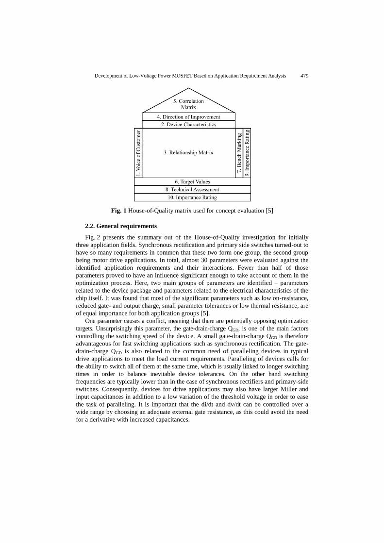
Within our work, the House-of-Quality Matrix was employed as an aid in determining how
products live up to customer needs [4]. Fig. 1 illustrates the basic worksheet used in this process
for analyzing the relationship between customer wishes and product capabilities and their
interactions, identifying development priorities and including a benchmarking of the new
concepts against predecessor products and the competition in the market. As the required inputs
are delivered from different functional units such as marketing, engineering and manufacturing,
the methodology also increases the cross-functional integration within the organization.
Development of Low-Voltage Power MOSFET Based on Application Requirement Analysis 479
Fig. 1 House-of-Quality matrix used for concept evaluation [5]
2.2. General requirements
Fig. 2 presents the summary out of the House-of-Quality investigation for initially
three application fields. Synchronous rectification and primary side switches turned-out to
have so many requirements in common that these two form one group, the second group
being motor drive applications. In total, almost 30 parameters were evaluated against the
identified application requirements and their interactions. Fewer than half of those
parameters proved to have an influence significant enough to take account of them in the
optimization process. Here, two main groups of parameters are identified – parameters
related to the device package and parameters related to the electrical characteristics of the
chip itself. It was found that most of the significant parameters such as low on-resistance,
reduced gate- and output charge, small parameter tolerances or low thermal resistance, are
of equal importance for both application groups [5].
One parameter causes a conflict, meaning that there are potentially opposing optimization
targets. Unsurprisingly this parameter, the gate-drain-charge QGD, is one of the main factors
controlling the switching speed of the device. A small gate-drain-charge QGD is therefore
advantageous for fast switching applications such as synchronous rectification. The gate-
drain-charge QGD is also related to the common need of paralleling devices in typical
drive applications to meet the load current requirements. Paralleling of devices calls for
the ability to switch all of them at the same time, which is usually linked to longer switching
times in order to balance inevitable device tolerances. On the other hand switching
frequencies are typically lower than in the case of synchronous rectifiers and primary-side
switches. Consequently, devices for drive applications may also have larger Miller and
input capacitances in addition to a low variation of the threshold voltage in order to ease
the task of paralleling. It is important that the di/dt and dv/dt can be controlled over a
wide range by choosing an adequate external gate resistance, as this could avoid the need
for a derivative with increased capacitances.
480 R, SIEMIENIEC, M. HUTZLER, O. BLANK, D. LAFORET, L. J. YIP, A. HUANG, R. WALTER
It is further known that avalanche events due to unclamped inductive switching can
affect the device in all addressed application fields. In case of single pulse events found
under critical operation conditions (as abrupt load changes, abrupt disconnection from the
power grid, blocked motors etc.) the energy which needs to be dissipated by the device
can be large. Also, the peak current density may exceed the nominal current rating. Here a
good suppression of the unwanted turn-on of the parasitic BJT is required and given for
most modern MOSFETs. However, the avalanche capability is limited by the intrinsic
temperature of the device where the intrinsic carrier density equals the background
doping, leading to thermal destruction of the device [6],[7],[8]. As active device areas
become smaller due to a lower specific on-resistance not only the overall device volume
for energy dissipation gets smaller but also the current densities increase. Also the thermal
resistance from junction to case RthJC increases at smaller chip sizes which imposes
another challenge in order to maintain the required device robustness.
Fig. 2 Requirements for synchronous rectification and primary-side switch applications
(left) and motor drive applications (right) [5]
A first conclusion to draw out of this analysis is that just one technology needs to be
developed since it is relatively easy to adapt it later to get a derivate for the other field of
application in case it is really needed. The second conclusion underlines the need for further
improved package technologies. Here, the most important requirements are a further reduction
of the package contribution to the overall on-resistance of the product and improved cooling
capabilities (lower RthJC). However, it is not only the package contribution to the on-resistance
of the device that matters, but also the parasitic inductance which it introduces. The inductance
due to the package leads to additional switching losses, slower switching speed, or may even
cause an unwanted turn-on of the device, all lowering the overall efficiency of the power-
electronic device. This parasitic inductance might also trigger repetitive avalanche events. The
number of repeated avalanche cycles, even when dissipating low energies in the range of 1 µJ
only, may affect the semiconductor in case of poor device designs.
2.3. Specific synchronous rectification requirements
The power losses in the MOSFET must be separated into load dependent conduction
losses and constant switching losses [9]. Conduction losses are determined by the RDS(ON)
of the switch. They increase with increasing output load of the power supply. On the other
hand the switching losses are constant over the whole output load, and are mainly
determined by the gate charge QG and the output charge QOSS.

Development of Low-Voltage Power MOSFET Based on Application Requirement Analysis 481
Fig. 3 Simplified model of the Synchronous Rectification MOSFET turn-off [9]
Further considering the turn-off process, also the stored charge QRR of the body diode
must be removed and the output capacitance COSS, formed by the gate-drain-capacitance CGD
and the drain-source-capacitance CDS, has to be charged up to the input voltage of the SR
stage as explained in Fig. 3. This process results in a reverse current peak IRRM which is
linked to the overall inductance of the commutation loop. The energy stored in this
inductance is transferred to the output capacitance as soon as the drain-source-voltage VDS of
the MOSFET exceeds the input voltage VIN with a voltage spike carrying this energy. The
amount of energy is defined by the reverse-recovery charge stored in the body diode QRR
and the charge stored in the output capacitance QOSS and is lost in every switching cycle.
A high QOSS + QRR does not only generate power losses but also causes a large reverse
current peak IRRM as shown schematically in Fig. 3. The higher the reverse current peak,
the higher the rate of voltage rise dv/dt, and thus the greater the turn-off voltage spike,
will be. This high dv/dt can also trigger a dynamic re-turn-on of the MOSFET by raising
the gate voltage above the threshold voltage due to the capacitive voltage divider
CGD / CGS as depicted in Fig. 4 [10]. To prevent this, a small output capacitance COSS, a small
stored charge QRR, a non-critical ratio CGD / CGS and a narrow tolerance of all MOSFET
capacitances are essential.
Fig. 4 Dynamic turn-on of a MOSFET by large dv/dt [10]

482 R, SIEMIENIEC, M. HUTZLER, O. BLANK, D. LAFORET, L. J. YIP, A. HUANG, R. WALTER
2.4. How to gain highest efficiency
To optimize the power MOSFET for highest efficiency, a well-balanced ratio between
switching losses and conduction losses must be found. At low output loads the conduction
losses only play a minor role while switching losses are dominant. For higher loads the
weighting of the losses is the other way around. To calculate the losses and to get an
indication how the technology will perform in the system, different figures-of-merit
(FOM) need to be considered [11],[12]. The FOMG is the product of the RDS(ON) and the
QG, while the FOMOSS is the product of RDS(ON) and QOSS. As the capacitances of a MOSFET
are inversely proportional to the RDS(ON), this product is fixed over the whole RDS(ON)
range of a given technology. Fig. 5 illustrates the derived relation between on-resistance
and overall power losses on example of a synchronous rectifier. As illustrated herein, the
conduction losses increase linearly with higher RDS(ON).
Since switching losses increase at low RDS(ON) values, a local minimum is found
considering the total power losses [13]. Here the MOSFET generates the lowest losses in
a given system and therefore the highest efficiency is found. Further optimization of a
synchronous rectification system cannot be done within this given MOSFET technology.
Consequently, the main goal of a new synchronous rectification MOSFET is moving this
point of minimum losses to the bottom left corner in Fig. 5. This can only be achieved by
a further massive reduction of switching losses and conduction losses at the same time.
This will raise the whole system efficiency both at low output power and at high output
power. An improvement of the FOMOSS will mainly affect the system efficiency at low
output power while the RDS(ON) will primarily affect the efficiency at high currents. Also
the stored charge QRR negatively affects the system efficiency at medium and high output
power and adequate measures might be required to reduce it.
These considerations are also valid for motor-drives, however the usually lower
switching frequency shifts the optimum point to a significantly reduced on-resistance.
Fig. 5 Power losses per device vs. on-resistance in synchronous rectification for a given
60 V MOSFET technology (VIN = 30 V, VGS = 10 V, I = 15 A, f = 125 kHz) [13]

Development of Low-Voltage Power MOSFET Based on Application Requirement Analysis 483
3. POWER SEMICONDUCTOR OPTIMIZATION
3.1. Introduction of device concept
The device concept discussed is related to a field-
plate trench MOSFET as shown schematically in Fig. 6.
Such devices entered the market more than 10 years ago
and developed into a kind of standard technology for
fast-switching devices. The basics and properties of
these devices have been discussed in more details in
many publications over the years, e.g [14]-[18].
The basic principle to realize an area-specific on-
resistance well below the 1D silicon limit [19],[20] is
similar to the charge-compensation principle in super-
junction devices like the CoolMOS™, as schematically
shown in Fig. 7a. Here the compensation of n-drift region
donors is realized by acceptors located in p-columns. In
field-plate type devices, an isolated field-plate provides
the mobile charges required to compensate the drift region
donors under blocking conditions as indicated in Fig. 7b.
a) b)
Fig. 7 a) Compensation by p- & n-columns; b) Compensation using a field-plate
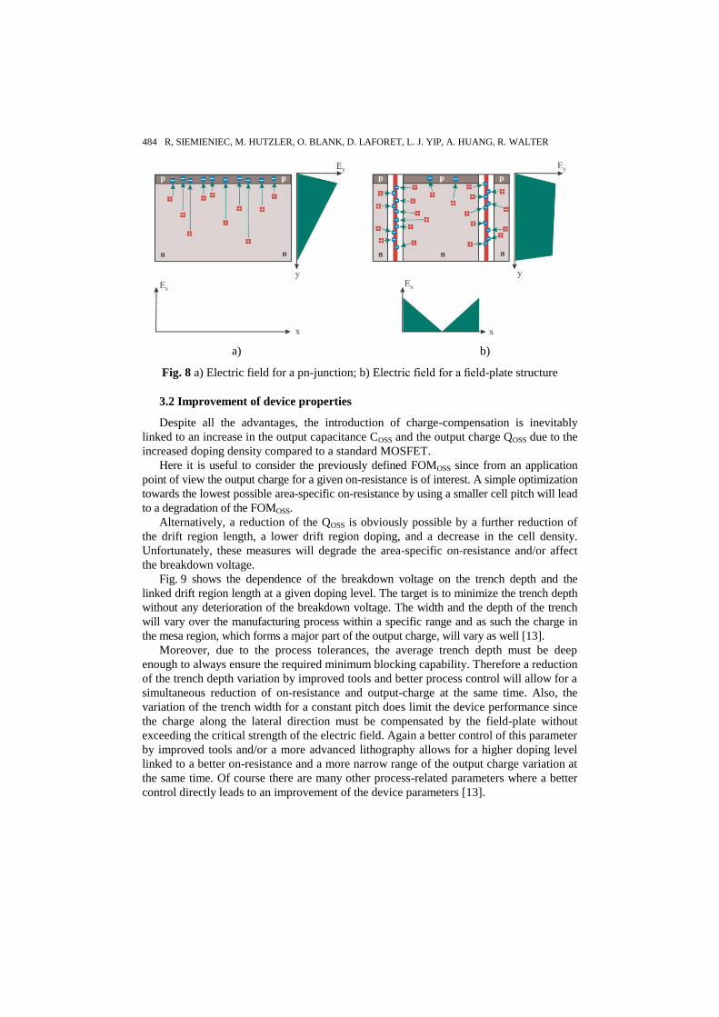
Compared to a device using a simple planar pn-junction, the electric field now also
has a component in the lateral direction. Fig. 8 explains the basic differences in the
electric field for a simple pn-junction and for the case where a field-plate compensates the
donors in the drift region. The application of a field-plate leads to an almost constant field
distribution in the vertical direction since the ionized dopants in the drift region are
laterally compensated by mobile carriers in the field-plate, thereby reducing the necessary
drift region length and increasing the allowed drift region doping for a given breakdown
voltage. Both contribute to the significantly reduced area-specific on-resistance. Since the
field-plate electrode is connected to the source electrode of the MOSFET and the gate is
formed by a separate electrode, such a device offers an outstanding area-specific on-
resistance and a low gate-charge at the same time.
Fig. 6 Schematic structure of
a field-plate MOSFET
484 R, SIEMIENIEC, M. HUTZLER, O. BLANK, D. LAFORET, L. J. YIP, A. HUANG, R. WALTER
a) b)
Fig. 8 a) Electric field for a pn-junction; b) Electric field for a field-plate structure
3.2 Improvement of device properties
Despite all the advantages, the introduction of charge-compensation is inevitably
linked to an increase in the output capacitance COSS and the output charge QOSS due to the
increased doping density compared to a standard MOSFET.
Here it is useful to consider the previously defined FOMOSS since from an application
point of view the output charge for a given on-resistance is of interest. A simple optimization
towards the lowest possible area-specific on-resistance by using a smaller cell pitch will lead
to a degradation of the FOMOSS.
Alternatively, a reduction of the QOSS is obviously possible by a further reduction of
the drift region length, a lower drift region doping, and a decrease in the cell density.
Unfortunately, these measures will degrade the area-specific on-resistance and/or affect
the breakdown voltage.
Fig. 9 shows the dependence of the breakdown voltage on the trench depth and the
linked drift region length at a given doping level. The target is to minimize the trench depth
without any deterioration of the breakdown voltage. The width and the depth of the trench
will vary over the manufacturing process within a specific range and as such the charge in
the mesa region, which forms a major part of the output charge, will vary as well [13].
Moreover, due to the process tolerances, the average trench depth must be deep
enough to always ensure the required minimum blocking capability. Therefore a reduction
of the trench depth variation by improved tools and better process control will allow for a
simultaneous reduction of on-resistance and output-charge at the same time. Also, the
variation of the trench width for a constant pitch does limit the device performance since
the charge along the lateral direction must be compensated by the field-plate without
exceeding the critical strength of the electric field. Again a better control of this parameter
by improved tools and/or a more advanced lithography allows for a higher doping level
linked to a better on-resistance and a more narrow range of the output charge variation at
the same time. Of course there are many other process-related parameters where a better
control directly leads to an improvement of the device parameters [13].
Development of Low-Voltage Power MOSFET Based on Application Requirement Analysis 485
Fig. 9 Breakdown voltage dependence on trench depth and linked drift region length for a
given doping [13]
Independent of the exact device structure, these thoughts can be transferred to any
similar device design. As example, Fig. 10 indicates the result for different ways of
optimizing the FOMOSS vs. RDS(ON) x Aactive. Despite the clear improvement of both key
parameters in the sweet spot, there are two particularly interesting facts to note. First, the
strong reduction of the output-charge results in only a minor increase in the area-specific
on-resistance compared to what would be achieved by a straightforward reduction of the
on-resistance. Second, also the FOMOSS of such an optimized device is competitive to
devices with pure focus on output charge reduction.
Fig. 10 Comparison of device performance of 1st and 2
nd generation field-plate trench
MOSFET to a standard trench MOSFET in the 60 V class
486 R, SIEMIENIEC, M. HUTZLER, O. BLANK, D. LAFORET, L. J. YIP, A. HUANG, R. WALTER
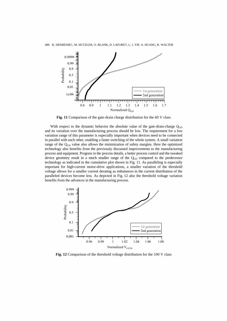
Fig. 11 Comparison of the gate-drain charge distribution for the 60 V class
With respect to the dynamic behavior the absolute value of the gate-drain-charge QGD
and its variation over the manufacturing process should be low. The requirement for a low
variation range of this parameter is especially important when devices need to be connected
in parallel with each other, enabling a faster switching of the whole system. A small variation
range of the QGD value also allows the minimization of safety margins. Here the optimized
technology also benefits from the previously discussed improvements to the manufacturing
process and equipment. Progress in the process details, a better process control and the tweaked
device geometry result in a much smaller range of the QGD compared to the predecessor
technology as indicated in the cumulative plot shown in Fig. 11. As paralleling is especially
important for high-current motor-drive applications, a smaller variation of the threshold
voltage allows for a smaller current derating as imbalances in the current distribution of the
paralleled devices become less. As depicted in Fig. 12 also the threshold voltage variation
benefits from the advances in the manufacturing process.
Fig. 12 Comparison of the threshold voltage distribution for the 100 V class

Development of Low-Voltage Power MOSFET Based on Application Requirement Analysis 487
4. PACKAGING ISSUES
With silicon technology moving rapidly forward the package becomes an increasingly
important part for low-voltage MOSFETs. The on-resistance of the latest device technologies
has become remarkably low; the package proportion of the overall on-resistance has
changed from a negligible 1:10 to 1:1 or even worse. In the past this need for low-resistive
packages to avoid a limitation of the device by the package characteristics drove the
development of new packages, optimized for high currents and high switching frequencies.
This becomes clear when referring to the package contributions of the discussed low-
voltage MOSFET devices with maximum die-size for the given package in Fig. 13. These
advanced device technologies allow for MOSFET dies in a still widely used TO-220 with
an on-resistance being equal to or lower than the package resistance. Therefore, the package
resistance clearly limits the minimum achievable on-resistance as it is explained on example
of three generations of 100 V devices with maximum die size in the respective package
shown in Fig. 14. For a TO-220 device, only 50 % of the gained on-resistance improvement
on chip level is realized in the packaged device due to the significant package contribution.
To follow the route towards denser and more efficient power converter designs, available
surface-mounted package types, such as the new TO-Leadless (TO-LL) [21], the SuperSO8,
the Shrinked SuperSO8 (S3O8) or the CanPAK™, are needed to replace the leaded SMD
or through-hole devices for low-voltage MOSFETs as they contribute significantly less to
the overall on-resistance of the product.
Fig. 13 Package contribution to the overall on-resistance for devices of different voltage
classes of the latest generation with maximum die-size in the respective package
Of course it is not only the package contribution to the on-resistance of the device
which matters, but also the parasitic inductance it introduces. At increasing switching
frequencies and switching speeds, the package inductance can play a major part in loss
generation for the overall device and application performance. For example, a buck-converter
with an output current of 30 A, operating at 250 kHz, generates 0.7 W of losses in a D-

488 R, SIEMIENIEC, M. HUTZLER, O. BLANK, D. LAFORET, L. J. YIP, A. HUANG, R. WALTER
PAK design due to the total package inductance of 6 nH. With a low-inductive package like the
SuperSO8, showing an inductance of less than 0.5 nH, these losses drop below 0.1 W.
However, most surface-mounted devices available so far were less suited for high-
current applications due to their limited footprint area and the corresponding limited
current-density due to the package itself. A recent solution addressing such applications is
the already mentioned TO-Leadless (TO-LL), which offers a lower parasitic resistance
and inductance, a lower thermal resistance and a higher current capability [21]. This
solution also extends the maximum allowed continuous current capability compared to the
commonly available TO-packages such as TO-220 or D²PAK 7-pin up to 300 A as it
offers a 50 % bigger solder contact area. This reduces the current density through the
solder contact areas and thus avoids electromigration issues at high current levels.
Fig. 14 Typical on-resistance reduction comparison of three 100 V MOSFET generations
on chip and package level
5. DEVICE PERFORMANCE
5.1. Efficiency and voltage overshoot
Improvements of the MOSFET die itself are mainly based on a detailed understanding
of the device physics and consequent improvement of manufacturing capabilities as
discussed briefly in this work or more detailed in [13]. The improvements realized by the
new 2nd
generation 80 V and 100 V MOSFETs over the equivalent 1st generation products
were investigated in a 400 W Power Supply (PSU) based on a full-bridge converter with
full wave synchronous rectification as schematically shown in Fig. 15.
For the efficiency evaluation, the synchronous rectifier stage was equipped with either
80 V or 100 V devices:
for 80 V: one 1st generation / 4.7 m device or
one 2nd
generation / 3 m device.
for 100 V: two paralleled 1st generation / 4.6 m devices or
two paralleled 2nd
generation / 4 m devices.

Development of Low-Voltage Power MOSFET Based on Application Requirement Analysis 489
Fig. 15 Simplified schematic of a 400 W / 33 A PSU using a full-bridge converter on the
primary side and full wave synchronous rectification
Fig. 16 compares the measured efficiency over the full load range of the PSU equipped
with 1st generation or 2
nd generation devices in the synchronous rectifier stage.
While the on-resistance of the 2nd
generation device is much lower, resulting in the better
high-load efficiency, the efficiency at low and medium load conditions is also maintained
due to the improved FOMOSS. By choosing the right on-resistance of the device, efficiency
can be easily improved over the full load range.
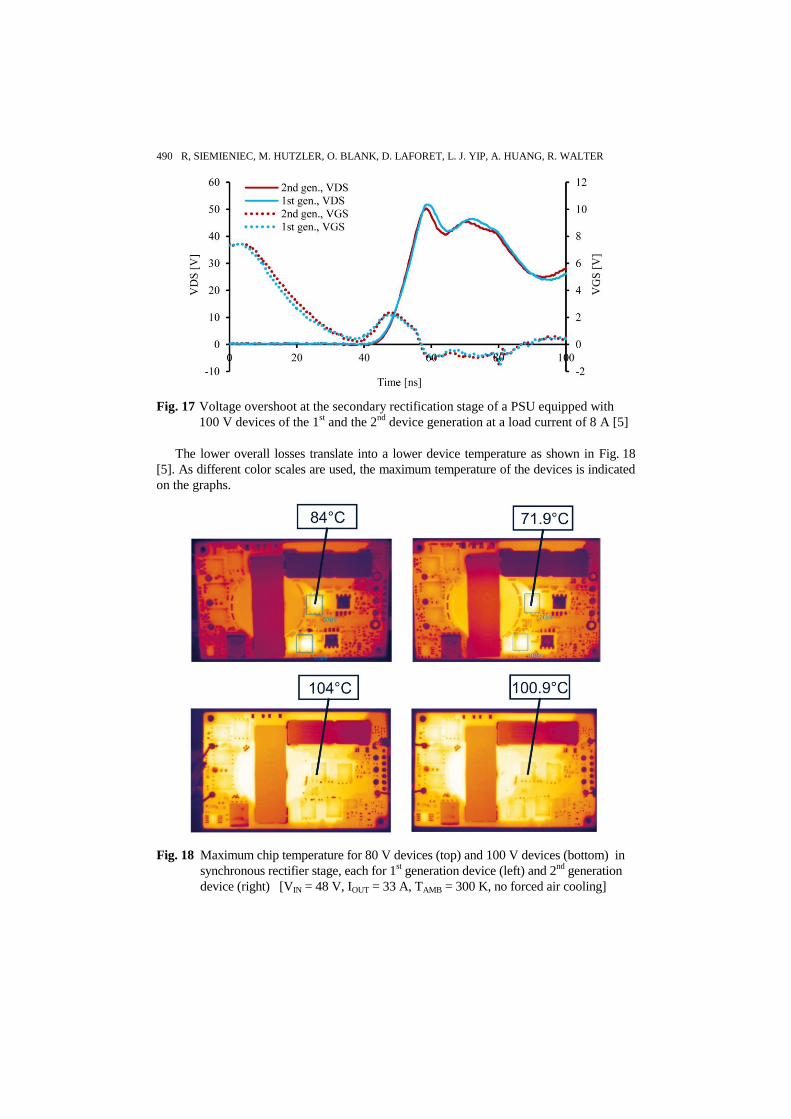
Fig. 17 indicates the voltage overshoot at the synchronous rectification switches for
the example of the 100 V devices at low load. Even at this condition the voltage spike is
lowered despite the higher degree of charge-compensation responsible for the lower on-
resistance. As designers need to ensure that the level of this peak does not exceed the
maximum rating of the device, a snubber network is commonly used which is costly and
typically decreases the performance of the power supply [22]. A snubber in its easiest
version consists of a series-connected resistor and capacitor connected in parallel to the
drain and source of the MOSFET. Any reduction its capacitance improves the efficiency
of the circuit and supports a lowered voltage spike of the power MOSFET.
Fig. 16 Comparison of the overall efficiency at an input voltage of 48 V [5]
490 R, SIEMIENIEC, M. HUTZLER, O. BLANK, D. LAFORET, L. J. YIP, A. HUANG, R. WALTER
Fig. 17 Voltage overshoot at the secondary rectification stage of a PSU equipped with
100 V devices of the 1st and the 2
nd device generation at a load current of 8 A [5]
The lower overall losses translate into a lower device temperature as shown in Fig. 18
[5]. As different color scales are used, the maximum temperature of the devices is indicated
on the graphs.
Fig. 18 Maximum chip temperature for 80 V devices (top) and 100 V devices (bottom) in
synchronous rectifier stage, each for 1st generation device (left) and 2
nd generation
device (right) [VIN = 48 V, IOUT = 33 A, TAMB = 300 K, no forced air cooling]

Development of Low-Voltage Power MOSFET Based on Application Requirement Analysis 491
5.2 Avalanche ruggedness
During development, the single-pulse avalanche destruction current was investigated
following a mixed-mode 2D simulation approach using two slightly different MOSFET
cells as proposed in earlier work [23]. The good agreement of the simulated and measured
destruction currents as shown in Fig. 19 indicates a proper chip design since no serious
degradation is introduced by the real, three-dimensional device structure.
Fig. 19 Measured and simulated single-pulse avalanche destruction current
To compare the avalanche capability of the 1st and 2
nd generation, single-pulse avalanche
measurements were done for different inductances and temperature values. Fig. 20 presents the
result of these measurements on example of 100 V devices having an identical active area. To
estimate the intrinsic temperature, extrapolation lines are fit to the average failure current
points determined at the various temperatures. The intersection point with the zero-current
line is found at the intrinsic temperature of the device.
The thermal destruction is found at approximately the same intrinsic temperature for
both device generations under identical conditions [7]. Consequently, the improved
device properties are not linked to an avalanche weakness.
Fig. 20 Measured avalanche capability vs. junction temperature for 100 V MOSFET

492 R, SIEMIENIEC, M. HUTZLER, O. BLANK, D. LAFORET, L. J. YIP, A. HUANG, R. WALTER
5.3 Performance of TO-LL package
As previously discussed, advanced package concepts enable a significant reduction of
the package contribution to the overall on-resistance of a device. How big this difference
can be is shown in a direct comparison between a D2PAK 7 pin and a TO-LL, both with
identical chip size. A typical application for such low resistive MOSFETs in a high current
package is the inverter for an electric 3-phase motor. Starting with a few tenths of an
Ampere, the continuous current easily reaches several hundred Amperes or more. A typical
battery voltage is 24 V therefore 60 V MOSFETs are an appropriate choice. The lowest
available on-resistance of such a device in D2PAK 7 Pin is 1 mΩ. This is the upper
guaranteed limit, including both silicon and package resistance. The package (= “copper“)
losses are already around 0.4 mΩ, representing nearly 50 % of the conduction losses. A
better solution would be a package with an improved design for lower copper losses. In
TO-LL with its optimized electrical and mechanical design, the package resistance goes down
to app. 0.25 mΩ. This enables a 60 V MOSFET with a maximum on-resistance of less than
0.75 mΩ. The reduction of package resistance results in dramatically lower losses, enabling, for
example, the chip temperature to be kept lower. Fig. 21 shows the chip temperature in a typical
motor control application (3-phase 24 V motor system, IRMS = 100 A) for the two packages,
D2PAK 7 Pin and TO-Leadless with identical chip size. After one hour the temperature
difference is already around 10 K. As a consequence the temperature stress to the TO-LL
parts is less, leading to an increased reliability of the parts linked to fewer failures in the
field and as such longer expected lifetimes [5].
Fig. 21 Evolution of chip temperature with time for 60 V MOSFET in a typical drives
application for devices with identical chip area in two different package types [5]
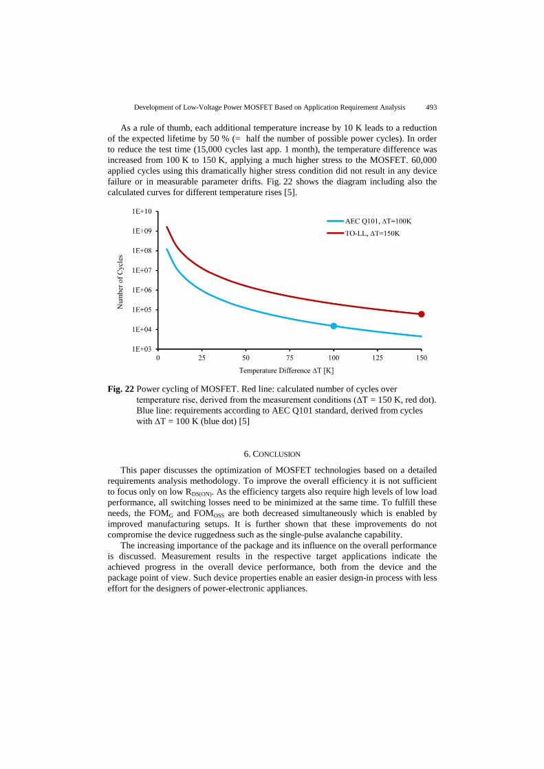
Using Intermittent Operating Lifetime tests (IOL), also called „Power Cycling“, the
reliability of the devices in the new TO-LL package was proven. In this test, the device is
heated up by a high current flow in each cycle until the defined temperature difference is
reached. The relevant industry standard AEC Q101 requires the device to survive a
minimum of 15,000 cycles at a temperature difference of 100 K.
Development of Low-Voltage Power MOSFET Based on Application Requirement Analysis 493
As a rule of thumb, each additional temperature increase by 10 K leads to a reduction
of the expected lifetime by 50 % (= half the number of possible power cycles). In order
to reduce the test time (15,000 cycles last app. 1 month), the temperature difference was
increased from 100 K to 150 K, applying a much higher stress to the MOSFET. 60,000
applied cycles using this dramatically higher stress condition did not result in any device
failure or in measurable parameter drifts. Fig. 22 shows the diagram including also the
calculated curves for different temperature rises [5].
Fig. 22 Power cycling of MOSFET. Red line: calculated number of cycles over
temperature rise, derived from the measurement conditions (∆T = 150 K, red dot).
Blue line: requirements according to AEC Q101 standard, derived from cycles
with ∆T = 100 K (blue dot) [5]
6. CONCLUSION
This paper discusses the optimization of MOSFET technologies based on a detailed
requirements analysis methodology. To improve the overall efficiency it is not sufficient
to focus only on low RDS(ON). As the efficiency targets also require high levels of low load
performance, all switching losses need to be minimized at the same time. To fulfill these
needs, the FOMG and FOMOSS are both decreased simultaneously which is enabled by
improved manufacturing setups. It is further shown that these improvements do not
compromise the device ruggedness such as the single-pulse avalanche capability.
The increasing importance of the package and its influence on the overall performance
is discussed. Measurement results in the respective target applications indicate the
achieved progress in the overall device performance, both from the device and the
package point of view. Such device properties enable an easier design-in process with less
effort for the designers of power-electronic appliances.

494 R, SIEMIENIEC, M. HUTZLER, O. BLANK, D. LAFORET, L. J. YIP, A. HUANG, R. WALTER
REFERENCES
[1] http://www.plugloadsolutions.com/80PlusPowerSupplies.aspx.
[2] Y. Akao. QFD - Quality Function Deployment. Verlag Moderne Industrie, Landsberg / Lech, 1992.
[3] http://www.qfdonline.com/.
[4] http://www.webducate.net/qfd/qfd.html.
[5] R. Siemieniec, M. Hutzler, D. Laforet, L.-J. Yip, A. Huang and R. Walter, "Application-tailored
development of Power MOSFET", in Proc. ISPS 2014, Prague, 2014.
[6] S. K. Ghandhi, Semiconductor Power Devices: Physics of Operation and Fabrication Technology, John
Wiley and Sons, New York, 1977.
[7] D. Kinzer, "Advances in power switch technology for 40V - 300V applications", in Proc. EPE 2005,
Dresden, 2005.
[8] J. Lutz, H. Schlangenotto, U. Scheuermann and R. de Doncker, Semiconductor Power Devices,
Springer, 2011, pp. 419-421.
[9] C. Mößlacher and L. Görgens, "Improving Efficiency of Synchronous Rectification by Analysis of the
Mosfet Power Loss Mechanism", in Proc. PCIM 2009, Nürnberg, 2009.
[10] L. Görgens and R. Siemieniec, "Niedriger Widerstand und kurze Schaltzeiten - OptiMOS-2 - 100V-
MOSFETs für Leistungsanwendungen mit hohem Wirkungsgrad", in Elektronik, pp. 60 - 63, June, 2006.
[11] A. Nakagawa, Y. Kawaguchi and K. Nakamura, "Silicon Limit Electrical Characteristics of Power
Devices and ICs", in Proc. ISPS 2008, Prague, 2008, pp. 25-32.
[12] C. Mößlacher and L. Görgens, "Simple design techniques for optimizing efficiency and overvoltage
spike of synchronous rectification in DC to DC converters", in Proc. PCIM 2010, Nürnberg, 2010.
[13] R. Siemieniec, C. Mößlacher, O. Blank, M. Rösch, M. Frank and M. Hutzler, "A new Power MOSFET
Generation designed for Synchronous Rectification", in Proc. EPE 2011, Birmingham, 2011.
[14] A. Schlögl, F. Hirler, J. Ropohl, U. Hiller, M. Rösch, N. Soufi-Amlashi and R. Siemieniec, "A new
robust power MOSFET family in the voltage range 80 V-150 V with superior low RDSon, excellent
switching properties and improved body diode", in Proc. EPE 2005, Dresden, 2005.
[15] J. Yedinak, D. Probst, G. Dolny, A. Challa and J. Andrews, "Optimizing Oxide Charge Balanced
Devices for Unclamped Inductive Switching (UIS) ", in Proc. ISPSD 2010, Hiroshima, 2010.
[16] F. Tong, P.A. Mawby, J.A. Covington and A. Pérez-Tomás, "Investigation on Split-Gate RSO MOSFET
for 30V Breakdown", in Proc. ISPS 2008, Prague, 2008.
[17] D. Pattanyak, "Low Voltage Super Junction technology", in Proc. ISPS 2006, Prague, 2006.
[18] J. Roig, D. Lee, F. Bauwens, B. Burra, A. Rinaldi, J. McDonald and B. Desoete, "Suitable Operation
Conditions for Different 100V Trench-Based Power MOSFETs in 48V-input Synchronous Buck
Converters", in Proc. EPE 2011, Birmingham, 2011.
[19] C. Hu, "A parametric study of power MOSFETs", in Proc. PESC 1979, San Diego, 1979, pp. 385-395.
[20] I. Pawel, R. Siemieniec and M. Born, "Theoretical Evaluation of Maximum Doping Concentration,
Breakdown Voltage and On-state Resistance of Field-Plate Compensated Devices", in Proc. ISPS 2008,
Prague, 2008, pp. 55-61.
[21] Infineon Technologies AG: OptiMOS™ in TO-Leadless, Product Brief, http://www.infineon.com
[22] R. Severns, "Design of Snubbers for Power Circuits", http://www.cde.com/resources/technical-
papers/design.pdf, July 2009.
[23] I. Pawel and R. Siemieniec, A New Simulation Approach to Investigate Avalanche Behaviour, in K.
Elleithy (Ed.): Innovations and Advanced Techniques in Systems, Computing Sciences and Software
Engineering, Springer, 2008, pp. 9-14.