Development of a Co deposition method for Deposition ... · Schematic Diagram of Sequential...
41
Development of a Co–deposition method for Deposition of Low–Contamination Pyrite Thin Films by Aditya Walimbe A Thesis Presented in Partial Fulfillment of the Requirements for the Degree Master of Science Approved April 2016 by the Graduate Supervisory Committee: Nathan Newman, Chair Rakesh Singh Terry Alford ARIZONA STATE UNIVERSITY May 2016
Transcript of Development of a Co deposition method for Deposition ... · Schematic Diagram of Sequential...

Development of a Co–deposition method for Deposition
of Low–Contamination Pyrite Thin Films
by
Aditya Walimbe
A Thesis Presented in Partial Fulfillment
of the Requirements for the Degree
Master of Science
Approved April 2016 by the
Graduate Supervisory Committee:
Nathan Newman, Chair
Rakesh Singh
Terry Alford
ARIZONA STATE UNIVERSITY
May 2016

i
ABSTRACT
Pyrite is a 0.95 eV bandgap semiconductor which is purported to have great
potential in widespread, low–cost photovoltaic cells. A thorough material selection process
was used in the design of a pyrite sequential vapor deposition chamber aimed at reducing
and possibly eliminating contamination during thin film growth. The design process
focused on identifying materials that do not produce volatile components when exposed to
high temperatures and high sulfur pressures. Once the materials were identified and design
was completed, the ultra–high vacuum growth system was constructed and tested.
Pyrite thin films were deposited using the upgraded sequential vapor deposition
chamber by varying the substrate temperature from 250°C to 420°C during deposition,
keeping sulfur pressure constant at 1 Torr. Secondary Ion Mass Spectrometry (SIMS)
results showed that all contaminants in the films were reduced in concentration by orders
of magnitude from those grown with the previous system. Characterization techniques of
Rutherford Back–scattering Spectrometry (RBS), X–Ray Diffraction (XRD), Raman
Spectroscopy, Optical Profilometry and UV/Vis/Near–IR Spectroscopy were performed
on the deposited thin films. The results indicate that stoichiometric ratio of S:Fe, structural–
quality (epitaxy), optical roughness and percentage of pyrite in the deposited thin films
improve with increase in deposition temperature. A Tauc plot of the optical measurements
indicates that the pyrite thin films have a bandgap of 0.94 eV.
ii
ACKNOWLEDGMENTS
I express my gratitude towards Prof. Nathan Newman, my research advisor, for
providing me the opportunity to undertake this project and his continuous guidance
throughout the project. I appreciate the motivation and encouragement he provided to help
me perform some challenging experiments in this project. I extend my thanks to Dr. Rakesh
Singh for his guidance and important discussions regarding results from Rutherford Back-
Scattering Spectrometry and for agreeing to serve on my Supervisory Committee. I am
grateful to Prof. Terry Alford for accepting to serve on my Supervisory Committee. I would
like to make a special mention of the help extended by Mr. Cameron Kopas and Mr. John
Domenico for XRD characterization, Mr. Cougar Garcia and Mr. Matthew Edwards for
RBS tool, simulation and analysis of the data, Mr. Aditya Ravi and Mr. Siddhesh Gajare
for helping me with electrical measurements and assembly of certain parts of chamber
itself. I am also grateful to Mr. Shengke Zhang and Mr. Makram Abd El Qader for
motivating me over the duration of my project. I thank Mr. Thomas Chamberlin for his
extensive support with SolidWorks in designing components of the chamber. I thank Mr.
James Makar from ASU machine shop for fabricating some vital parts of my chamber. I
am particularly grateful to Mr. Richard Henley for his continuous support in fixing
equipments and also procuring supplies required for the chamber. The use of facilities in
the LeRoy Eyring Center for Solid State Science at Arizona State University is
acknowledged. Last but not least, I would like to convey thanks to all other members of
Newman Research group for their constant support in carrying out this project.
iii
TABLE OF CONTENTS
Page
LIST OF TABLES………………………………………………………………………..iv
LIST OF FIGURES………………………………………………………………………..v
CHAPTER
1. INTRODUCTION…………………………………………………………….......1
2. MOTIVATION…………………………………………………………………....6
3. EXPERIMENTAL PROCEDURE………………………………………………..8
4. RESULTS AND DISCUSSIONS………………………………………………..16
5. CONCLUSIONS…...………………………………………………………........31
6. FUTURE WORK………………………………………………………………...32
7. REFERENCES…………………………………………………………………..33

iv
LIST OF TABLES
Table Page
1. Sulfides Present in Iron–Sulfur Phase Diagram…………………………..………..3
2. Enthalpy of Formation for Sulfides of Materials Chosen for the Study….……….17
3. Summary of SIMS Performed on Deposited Thin Films………………...…….…20
v
LIST OF FIGURES
Figure Page
1. Plot showing Dependence of Efficiency of Single–Junction Solar Cell on
Bandgap………...…………..…………………………………………………………1
2. Iron – Sulfur Binary Phase Diagram…………….………………….……………..…...3
3. Schematic Diagram of Sequential Evaporation System….…........................................4
4. Design of the Chamber used for Pyrite Thin Film Deposition showing Important
Parts……………………………….…………………..………….……………..……..9
5. Design of the Substrate Heater Assembly used in the Upgraded Chamber…………...10
6. Ellingham Diagram of Known Sulfides…………………..…………………………..11
7. Plot showing Profile of Process Parameters for Deposition at 350°C and 1 Torr…….12
8. Results of TGA for Al, Macor and SiO2–coated Stainless Steel Samples…………….17
9. RBS Plot for Al Sample showing Reaction Products and Layer Thicknesses………..18
10. RBS Plot for Macor Sample showing no Reaction with Sulfur………………………18
11. HeIXE Plot showing no Aluminum Contamination of Deposited Thin Film………..19
12. S:Fe Ratio in Deposited Thin Films Determined from RBS Simulation……………...22
13. FWHM of Pyrite (200) Peak in XRD Plots of Deposited Thin Films………………..23
14. Raman Spectra from Iron Sulfides Obtained using Green (523 nm) Excitation………24
15. Raman Spectra obtained from Natural Pyrite Samples…..…......................................24
16. Raman Spectra from Films with Pyrite:Marcasite Ratios of 99:1 and 49:51………….25
17. Plot showing increase in Proportion of Pyrite Phase with Deposition Temperature…26
18. Plot showing Relation between Roughness of Deposited Thin Films and Deposition
(Substrate) Temperature……………………………………………………………...26

vi
Figure Page
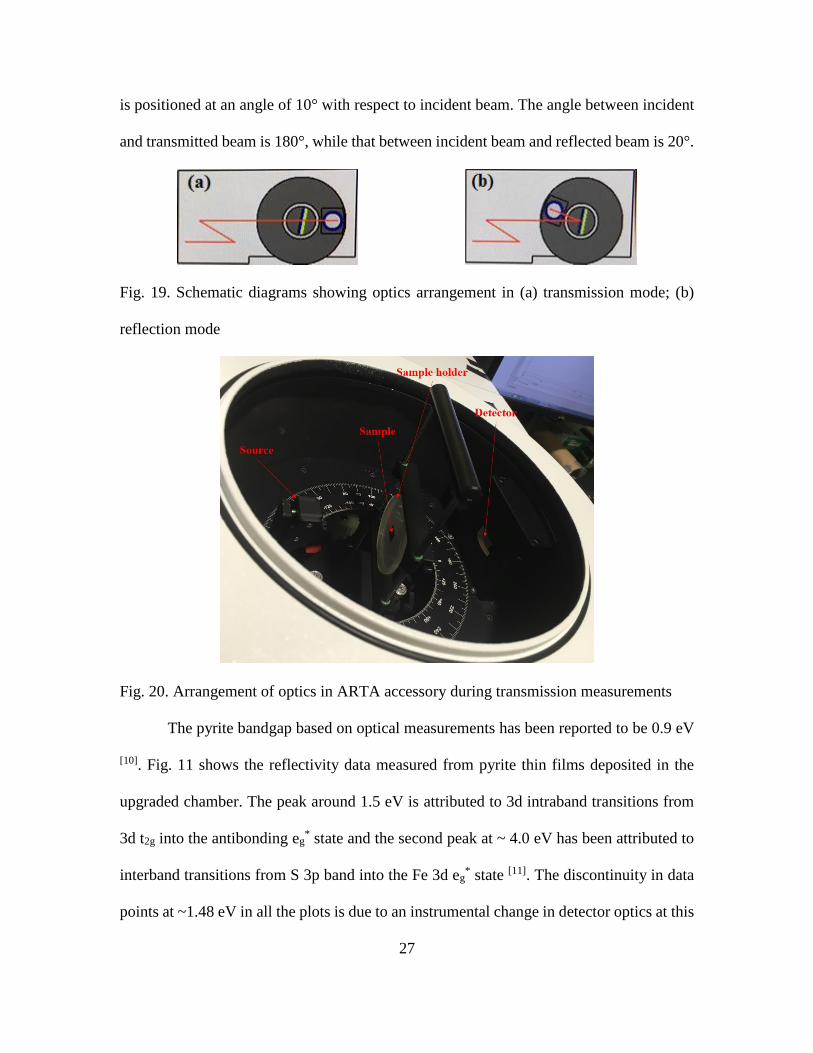
19. Schematic Diagrams showing Optics Arrangement in (a) Transmission Mode; (b)
Reflection Mode……………………………………………………………………...27
20. Arrangement of Optics in ARTA Accessory during Transmission Measurements…...27
21. Reflectivity Plot obtained from Deposited Pyrite Thin Films………………………...28
22. Transmission Data obtained from Deposited Pyrite Thin Films……………………...29
23. Variation in Absorption Coefficient with increasing Photon Energy…………………29
24. Estimation of Bandgap Energy of Pyrite Thin Films using Optical Method………...30

1
CHAPTER 1
INTRODUCTION
1.1 Operation and efficiency of single–cell photovoltaic cell
A p–n junction photovoltaic (PV) cell operates by absorbing a photon of light with
energy greater than or equal to bandgap of its material. The electrons and holes that are
generated drift to the edge of the depletion region and then through the semiconductor
neutral region and then, are collected at their respective electrodes. The efficiency of a PV
cell primarily depends on: (i) fraction of light with energies above the bandgap, (ii) energy
lost to thermalization of photons above the bandgap and (iii) the ratio between the time
charge carriers take to cross the depletion region and their lifetimes. According to Shockley
and Queisser [1], recombination between electrons and holes resulting in radiation, i.e.
radiative recombination, determines the detailed balance limit for efficiency by setting a
limit to minority carrier lifetimes. This theoretical limit of efficiency, also called Shockley–
Queisser limit, has maximum value of 30% at 1.1 eV bandgap exposed to sunlight of 1.5
global air mass, as shown in Fig. 1.
Fig. 1. Plot showing dependence of efficiency of single–junction solar cell on bandgap [1]
2
From the data published by Green, M. A. et al. (2015) [2], crystalline silicon (x–Si)
photovoltaic cells have obtained an efficiency of up to 25.6% ± 0.5%, when measured at
25°C in a global AM 1.5 spectrum (1000W/m2). On the other hand, low–cost photovoltaic
technologies such as amorphous silicon (a–Si) and micro–crystalline silicon have exhibited
efficiencies as high as 10.2% ± 0.3% and 11.4% ± 0.3%, respectively. Thin film cells
based on gallium arsenide (GaAs), chalcogenides such as copper indium gallium selenide
(CuInxGa1-xSe2; CIGS) and cadmium telluride (CdTe) respectively show cell efficiency of
28.8% ± 0.9%, 20.5% ± 0.6% and 21.0% ± 0.4% [2]. Due to its low absorption cross–
section and high processing cost, x–Si does not show promise for a low–cost, thin film PV
device. However, toxicity, scarcity and thereby the cost associated using As, In, Ga and Cd
in the GaAs, CIGS and CdTe cells limits their potential for wide–spread use in the future.
Thus, when seeking alternatives for present PV materials, these drawbacks along with the
need of decrease in cost, must be given prime importance.
Semiconductors like copper zinc tin sulfide (Cu2ZnSnS4; CZTS), pyrite (FeS2) and
copper oxide (CuO) have been identified as materials which could potentially overcome
the drawbacks of conventional PV materials and attain wide–spread use by the PV industry
in the future [3]. Each of these semiconductors are comprised on inexpensive materials and
have: (a) an appropriate bandgap for efficient conversion, (b) low toxicity, (c) low
extraction cost, and (d) a high absorption cross–section [4].
1.2 Pyrite as a candidate for thin film photovoltaic cells
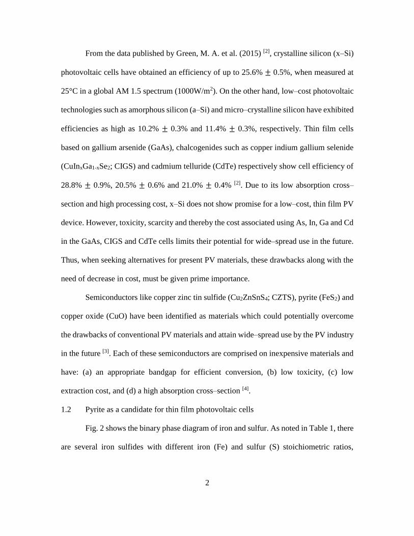
Fig. 2 shows the binary phase diagram of iron and sulfur. As noted in Table 1, there
are several iron sulfides with different iron (Fe) and sulfur (S) stoichiometric ratios,
3
different crystal structures and thus, different properties. This has proven to make the
synthesis of a phase–pure, high–quality pyrite thin film challenging.
Fig. 2. Iron – Sulfur binary phase diagram [5]
Table 1. Sulfides present in iron–sulfur phase diagram [5]
Phase Composition, wt. % S Crystal structure
γFeS 36.5 to 41 *
Troilite; βFeS 36.5 to ~38 Hexagonal
αFeS 36.5 to ~38 *
Pyrite; βFeS2 ~53.5 Cubic
Marcasite; αFeS2 ~53.5 Orthorhombic
* Crystal structure can be hexagonal or monoclinic.
4
1.3 Deposition of pyrite thin films
Experimental techniques used to grow pyrite thin films include chemical vapor
transport (CVT), metal–organic chemical vapor deposition (MOCVD), spray pyrolysis
methods and sulfurization of iron and iron oxides [4]. These methods extensively rely on
the use of chemical compound precursors which can be expensive and toxic.
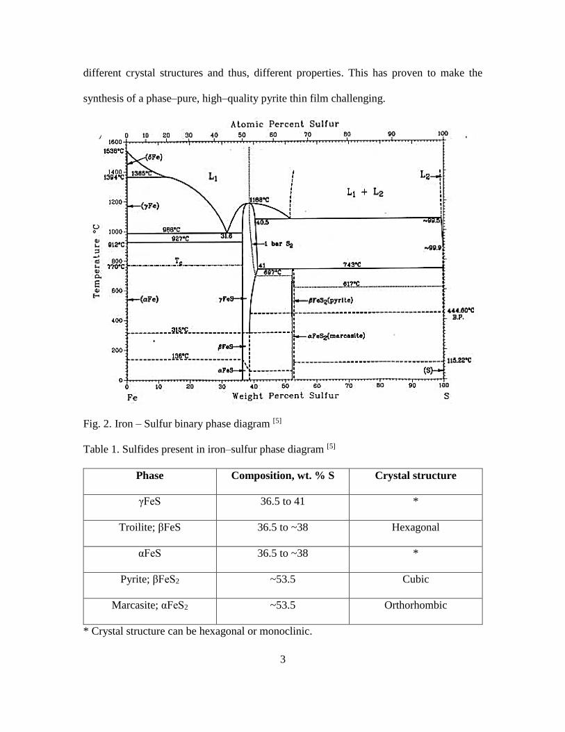
A high vapor pressure of sulfur is required when using physical vapor deposition
(PVD) techniques to synthesize pyrite. Vahidi M. et al. (2013) developed a simple and
robust PVD layer–by–layer growth process to make high–quality, single phase pyrite thin
films from their elemental constituents, S and Fe [6]. This technique was subsequently
modified by Wertheim A. to achieve better control of sulfur pressure and substrate
temperature. This is the sequential vapor deposition system in which heated substrates are
alternately exposed to iron in high vacuum and sulfur at high pressure (0.1 Torr – 1 Torr)
using a rotating substrate holder mechanism as seen in fig. 3.
Fig. 3. Schematic diagram of sequential evaporation system [6]

5
The films deposited in this system were found to have a significant level of
contamination in the thin films arising from re–evaporation of the reaction products
between sulfur and chamber components (eg. gaskets, substrate heater and electrical
feedthroughs). My work focused on reducing the concentration of contaminants and
improving the quality of deposited thin films. I have followed a similar deposition process,
however, growths were performed at higher sulfur pressure, i.e. 1 Torr. The following
chapters elaborate on the motivation for this project, the procedures followed when
conducting experiments, results of characterization techniques and conclusions based on
these results.

6
CHAPTER 2
MOTIVATION
In a study conducted by Wadia C. et al. (2009) [3], the potential to produce
inexpensive and efficient photovoltaics for widespread use was evaluate for 23 inorganic
semiconductors. The investigators took into account the single junction efficiency limits,
cost of extraction of respective raw materials, worldwide material reserves and the
electricity production potential.
Iron pyrite (FeS2), crystalline silicon (x–Si), amorphous silicon (a–Si) and gallium
arsenide have raw material cost of $1.9 x 10⁻⁸, $3.9 x 10⁻⁴, $1.8 x 10⁻⁶ and $2.5 x 10⁻³ for
every watt ($/W) of the potential amount of electricity produced by photovoltaic cells made
from these materials. About 55% of total installed cost for existing PV comes from the
module cost. If pyrite–based photovoltaic cells could be produced with inexpensive
methods and also achieve the same performance as x–Si, it could produce 102 to 103 times
the current global annual electricity consumption compared to 10-2 to 10-1 times achievable
by x–Si [3].
In chapter 1, I discussed fundamental aspects of operation, cell efficiency and
material choice for a photovoltaic cell. Large bandgap materials (> ~1.3 eV) absorb a
relatively small part of the available spectrum, thereby exhibiting smaller short–circuit
current (ISC), while small bandgap materials absorb broad section of the spectrum, but
exhibit a lower open–circuit voltage (VOC). Poor quality semiconductors with significant
concentrations of midgap levels have low carrier mobilities and minority–carrier lifetimes,
also resulting in poor cell efficiencies. Such performance degrading levels are formed by

7
native and impurity defects. Although the sequential evaporation process developed by my
group showed great promise to make stoichiometric, high–structural quality pyrite thin
films, methods to prevent high level of contamination during deposition had not been
developed. The primary objective of my project was reduction and elimination of
contaminants in deposited pyrite thin films.
8
CHAPTER 3
EXPERIMENTAL PROCEDURE
In this chapter, the procedures used to carry out the experiments in this project are
outlined. The first section, 3.1, describes the design, fabrication and testing of the new
upgraded growth system. In the second section, 3.2, procedures for depositing pyrite thin
films are elaborated. Finally, in section 3.3, the capabilities and methodology of
characterization techniques has been reviewed.
3.1 Design of substrate holder for upgraded chamber
The secondary ion mass spectrometry (SIMS) analysis performed on thin films
deposited using sequential vapor deposition chamber designed by Vahidi M. et al. [6]
indicated large concentrations of impurities such as copper (Cu), chromium (Cr), nickel
(Ni) and manganese (Mn). The copper impurity arose from re–evaporation of products of
reaction of sulfur with components of vacuum chamber, mainly, gaskets used for vacuum-
sealing flanges and electrical feedthroughs used to supply power to the heating elements.
The source of tungsten impurity was identified to be the iron–evaporation crucible. The
source for Ni, Cr and other constituents was the heated stainless steel substrate holder,
bottom–plate and bottom–disc. These components were exposed to high sulfur pressures
and temperatures (300°C – 450°C), which resulted in a strong reaction with sulfur. To
eliminate contamination, it is necessary to eliminate materials which react with sulfur and
form volatile products. Fig. 4 shows a schematic of the deposition chamber indicating main
components of the system.

9
Fig. 4. Design of the chamber used of pyrite thin film deposition showing important parts

10
Fig. 5. Design images of the substrate heater assembly used in the upgraded chamber
Some common metals, compounds and ceramics commonly used in vacuum
systems were chosen for investigation. For each candidate material, potential reaction
products formed when exposed to sulfur under the temperature and pressure conditions
present in chamber were determined using appropriate phase diagrams, including those
presented as Ellingham diagrams (fig. 6). To carry out this experiment, the amount of sulfur
required to attain a pressure of 100 Torr in the ampoule was determined. Then a specimen
of each candidate material was weighed, placed in a separate ampoule with appropriate
amount of sulfur and then vacuum–sealed. To test the materials under accelerated
degradation conditions, the ampoules were subsequently heated in a tubular furnace at
temperature to 450°C for 24 hours. After the heat treatment, each of the materials was
removed from the ampoules and characterized using X-Ray Diffraction (XRD) for phase
identification, Rutherford Back-scattering Spectrometry (RBS) for determination of the
thickness and composition of the reacted layer and Thermo-gravimetric Analysis (TGA)
for quantifying the volatility of the reaction products.
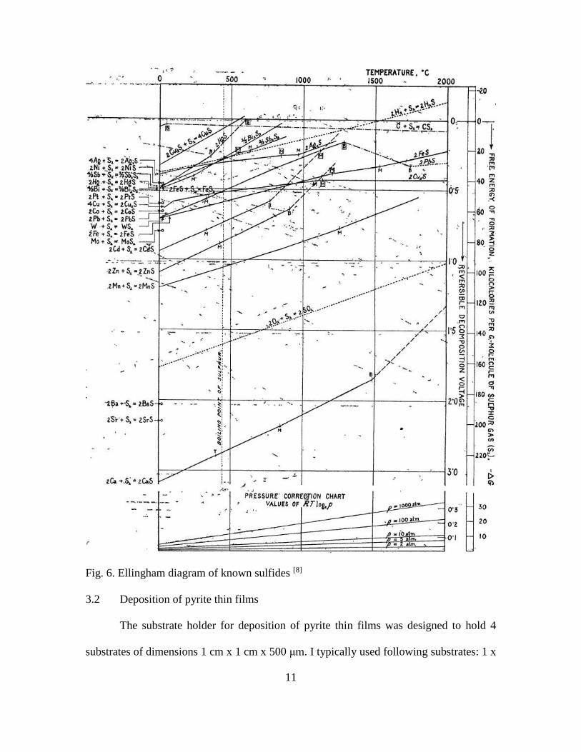
11
Fig. 6. Ellingham diagram of known sulfides [8]
3.2 Deposition of pyrite thin films
The substrate holder for deposition of pyrite thin films was designed to hold 4
substrates of dimensions 1 cm x 1 cm x 500 μm. I typically used following substrates: 1 x

12
Si (100), 2 x SiO2–coated Si and 1 x Al2O3 (r–plane) for the following reasons. Iron pyrite
(FeS2) and silicon (Si) both have a cubic structure and the lattice mismatch is only 0.25%
(FeS2: 5.418 Å; Si 5.431 Å). The SiO2–coated Si substrates have an amorphous and
insulating thermal–oxide buffer layer of approximately 2000 Å. Prior to loading substrates
in the chamber, the surfaces were cleaned by ultra–sonicating them in semiconductor–
grade acetone followed by isopropyl alcohol for 5 minutes. All substrates, except Si (100),
were rinsed with de–ionized (DI) water which was subsequently blown off with dry N2 gas
and then mounted onto the substrate holder. Silicon substrates were subjected to an
additional etch step in order to remove the native oxide layer from its surface. The Si
substrate surface was exposed for 3 minutes to a freshly prepared 5% (by volume) solution
of HF acid in DI water, followed by rinsing with DI water and blow–off with dry N2.
Immediately after this step, the Si substrate was mounted on the substrate holder, which
was subsequently loaded into the chamber and connected with the substrate heater
assembly. The chamber was then pumped down to high vacuum conditions and typically
left overnight to achieve a low base pressure (typically on the order of 1.2 × 10⁻⁵ Torr).
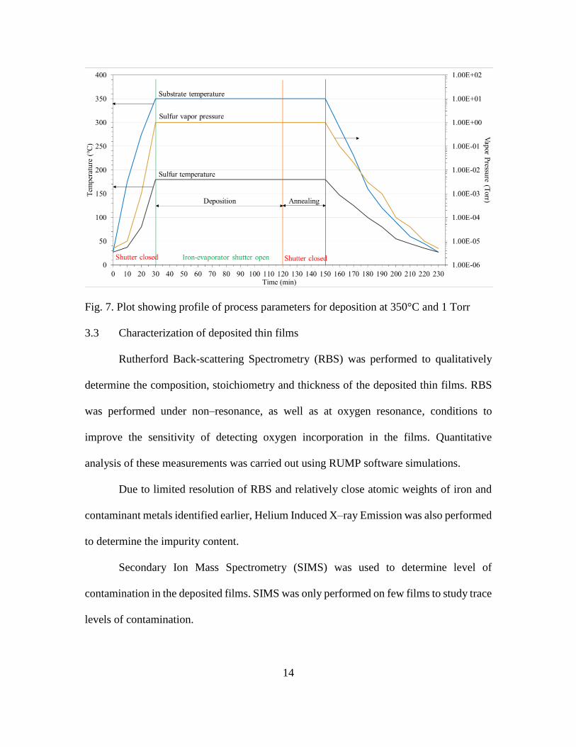
For conducting each deposition experiment, a single–step temperature sequence for
substrate heater was used. The raw materials used for deposition experiments were iron
(Alfa Aesar; 99.98% metals basis purity) and sulfur (STREM Chemicals; 99.999% purity)
loaded into their respective crucibles. Iron was evaporated from an alumina–coated
tungsten crucible heated by passing constant current (37.5 A) through it. The sulfur
pressure was maintained at either 100 mTorr or 1 Torr by heating sulfur–evaporation
crucible to corresponding temperature of 147°C or 180°C. Through the course of the
experiment, substrate holder along with substrate stage assembly was rotated inside the

13
substrate heater at rotation speed of ~5 rpm. The substrate temperature chosen for each
deposition was varied between 250°C and 425°C (in steps of 25°C). Substrates were heated
from room temperature to the deposition temperature, held at that temperature in presence
of iron–evaporation and sulfur at 1 Torr for growth duration (90 minutes), annealed at same
temperature for 30 minutes and then cooled to room temperature in vacuum. When the
substrates reached the deposition temperature and the sulfur crucible temperature was
stable at 147°C or 180°C, the iron–evaporation crucible was heated up to temperature in
~1 minute and its shutter was opened. After 90 minutes, the shutter was closed and the
current supplied to the iron–evaporation crucible was brought down to zero over a period
of 2 minutes. During annealing, the substrate temperature and 1 Torr sulfur pressure were
maintained at same values as during deposition. At the end of annealing stage, the current
supplied to the substrate heater as well as the sulfur–evaporation crucible was stopped and
the substrates were allowed to cool to room temperature. After each deposition, the
substrates with their deposited thin films were removed from the chamber for
characterization.
14
Fig. 7. Plot showing profile of process parameters for deposition at 350°C and 1 Torr
3.3 Characterization of deposited thin films
Rutherford Back-scattering Spectrometry (RBS) was performed to qualitatively
determine the composition, stoichiometry and thickness of the deposited thin films. RBS
was performed under non–resonance, as well as at oxygen resonance, conditions to
improve the sensitivity of detecting oxygen incorporation in the films. Quantitative
analysis of these measurements was carried out using RUMP software simulations.
Due to limited resolution of RBS and relatively close atomic weights of iron and
contaminant metals identified earlier, Helium Induced X–ray Emission was also performed
to determine the impurity content.
Secondary Ion Mass Spectrometry (SIMS) was used to determine level of
contamination in the deposited films. SIMS was only performed on few films to study trace
levels of contamination.

15
Glancing–angle X–ray Diffraction (GA–XRD) was performed on thin films
deposited on Si (100) substrates to determine the crystal quality of the primary phase and
the detection of any secondary phases of iron disulfide. Marcasite is a phase in iron-sulfur
phase diagram that has chemical composition FeS2 and although it has orthorhombic
crystal structure, peaks in the XRD pattern from both marcasite and pyrite occur at similar
values of 2θ. Raman Spectroscopy was also used to distinguish between pyrite and
marcasite as Raman shift occurs at distinct wavelengths for each of these phases.
Measurements were performed using an optical profilometer to investigate the
surface topography characteristics. Along with these, transmission and reflection
measurements were also performed in UV/Vis/Near–IR range of spectrum to measure the
absorption and absorbance of pyrite thin films with the aim of determining the bandgap of
iron pyrite and detecting any mid–gap levels that may be present.
16
CHAPTER 4
RESULTS AND DISCUSSIONS
4.1 Selection of material for substrate holder
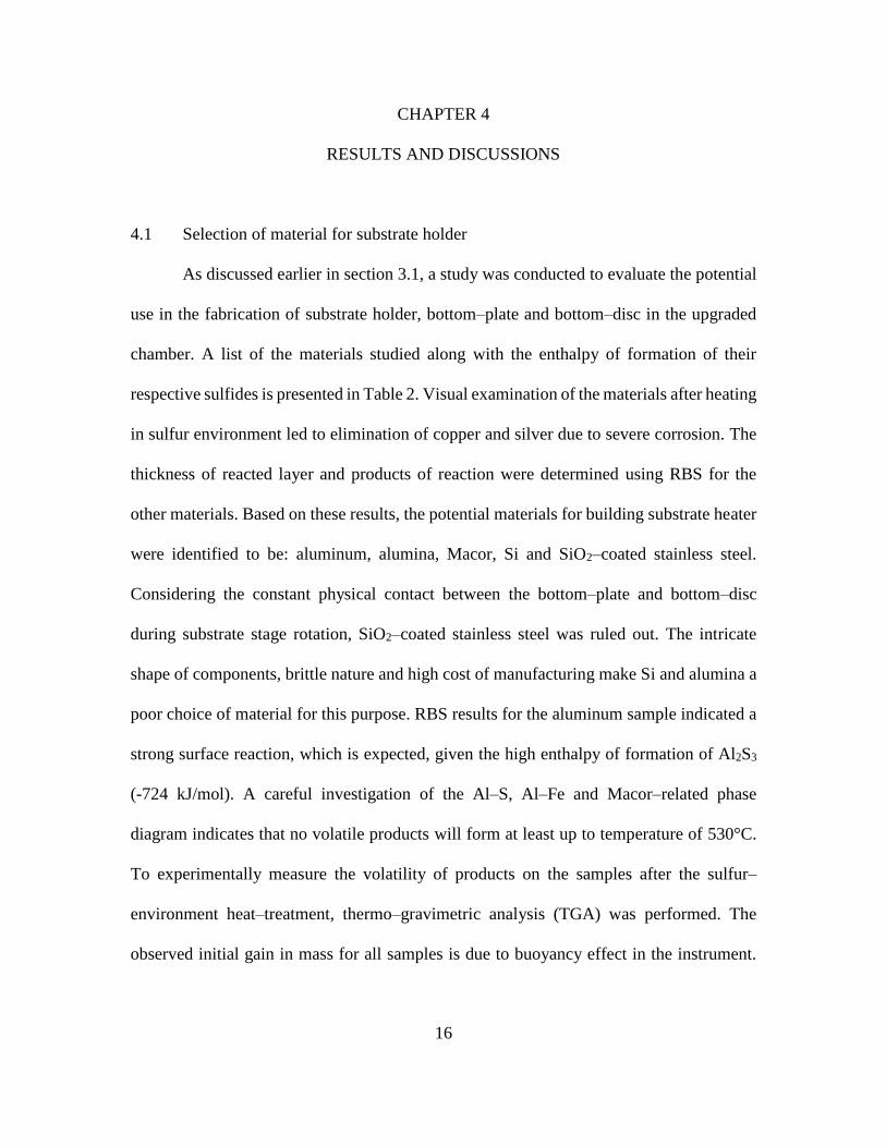
As discussed earlier in section 3.1, a study was conducted to evaluate the potential
use in the fabrication of substrate holder, bottom–plate and bottom–disc in the upgraded
chamber. A list of the materials studied along with the enthalpy of formation of their
respective sulfides is presented in Table 2. Visual examination of the materials after heating
in sulfur environment led to elimination of copper and silver due to severe corrosion. The
thickness of reacted layer and products of reaction were determined using RBS for the
other materials. Based on these results, the potential materials for building substrate heater
were identified to be: aluminum, alumina, Macor, Si and SiO2–coated stainless steel.
Considering the constant physical contact between the bottom–plate and bottom–disc
during substrate stage rotation, SiO2–coated stainless steel was ruled out. The intricate
shape of components, brittle nature and high cost of manufacturing make Si and alumina a
poor choice of material for this purpose. RBS results for the aluminum sample indicated a
strong surface reaction, which is expected, given the high enthalpy of formation of Al2S3
(-724 kJ/mol). A careful investigation of the Al–S, Al–Fe and Macor–related phase
diagram indicates that no volatile products will form at least up to temperature of 530°C.
To experimentally measure the volatility of products on the samples after the sulfur–
environment heat–treatment, thermo–gravimetric analysis (TGA) was performed. The
observed initial gain in mass for all samples is due to buoyancy effect in the instrument.
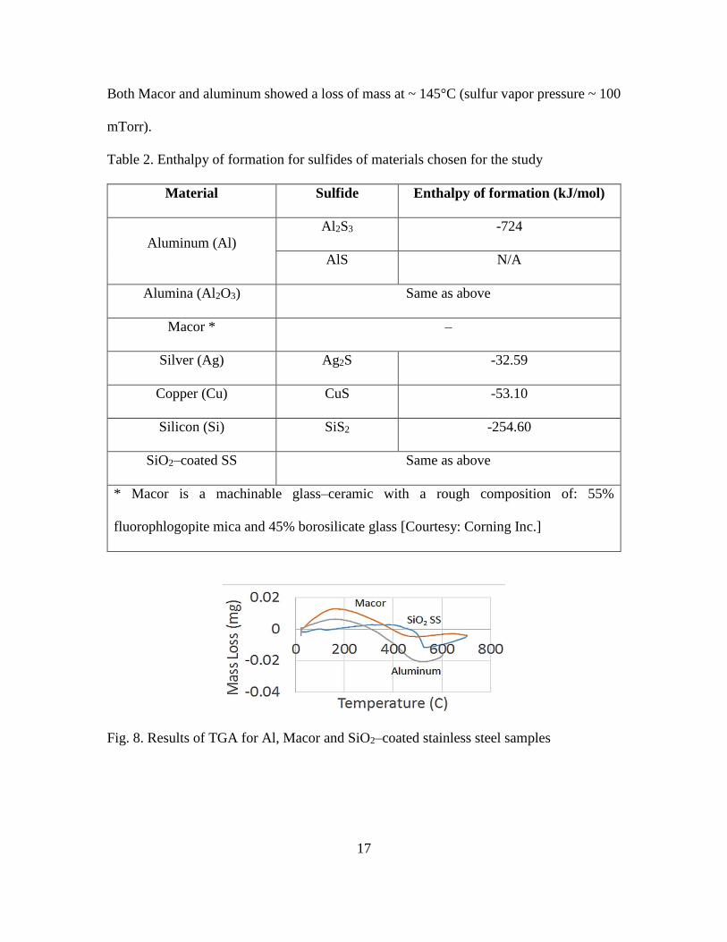
17
Both Macor and aluminum showed a loss of mass at ~ 145°C (sulfur vapor pressure ~ 100
mTorr).
Table 2. Enthalpy of formation for sulfides of materials chosen for the study
Material Sulfide Enthalpy of formation (kJ/mol)
Aluminum (Al)
Al2S3 -724
AlS N/A
Alumina (Al2O3) Same as above
Macor * –
Silver (Ag) Ag2S -32.59
Copper (Cu) CuS -53.10
Silicon (Si) SiS2 -254.60
SiO2–coated SS Same as above
* Macor is a machinable glass–ceramic with a rough composition of: 55%
fluorophlogopite mica and 45% borosilicate glass [Courtesy: Corning Inc.]
Fig. 8. Results of TGA for Al, Macor and SiO2–coated stainless steel samples

18
Fig. 9. RBS plot for Al sample showing reaction products and layer thicknesses
Fig. 10. RBS plot for Macor sample showing no reaction with sulfur

19
4.2 Helium Induced X–ray Emission (HeIXE)
Aluminum was used to fabricate the substrate holder and bottom–disc of the heater
assembly. Since the substrate holder surrounds and is also in direct physical contact with
the substrates for the entire duration of the growth, it is essential to check if aluminum
contaminates the deposited films in the upgraded chamber system. As mentioned in section
3.2, the pyrite thin films were deposited on silicon, thermally–oxidized silicon and sapphire
substrates.
HeIXE was performed on a thin film deposited (PTF073015) on magnesium oxide
(MgO) substrate. There was no detectable aluminum contamination in the deposited thin
films up to the detection limit of ~100 ppm as shown in the next figure.
Fig. 11. HeIXE plot showing no aluminum contamination of deposited thin film
20
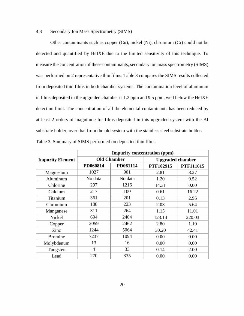
4.3 Secondary Ion Mass Spectrometry (SIMS)
Other contaminants such as copper (Cu), nickel (Ni), chromium (Cr) could not be
detected and quantified by HeIXE due to the limited sensitivity of this technique. To
measure the concentration of these contaminants, secondary ion mass spectrometry (SIMS)
was performed on 2 representative thin films. Table 3 compares the SIMS results collected
from deposited thin films in both chamber systems. The contamination level of aluminum
in films deposited in the upgraded chamber is 1.2 ppm and 9.5 ppm, well below the HeIXE
detection limit. The concentration of all the elemental contaminants has been reduced by
at least 2 orders of magnitude for films deposited in this upgraded system with the Al
substrate holder, over that from the old system with the stainless steel substrate holder.
Table 3. Summary of SIMS performed on deposited thin films
Impurity Element
Impurity concentration (ppm)
Old Chamber Upgraded chamber
PD060814 PD061114 PTF102915 PTF111615
Magnesium 1027 901 2.81 8.27
Aluminum No data No data 1.20 9.52
Chlorine 297 1216 14.31 0.00
Calcium 217 100 0.61 16.22
Titanium 361 201 0.13 2.95
Chromium 188 223 2.03 5.64
Manganese 311 264 1.15 11.01
Nickel 694 2404 123.14 220.03
Copper 2059 2462 2.80 1.19
Zinc 1244 5064 30.20 42.41
Bromine 7237 1094 0.00 0.00
Molybdenum 13 16 0.00 0.00
Tungsten 4 33 0.14 2.00
Lead 270 335 0.00 0.00

21
In order to eliminate contamination from copper, I replaced all copper gaskets with
alternate materials. Aluminum gaskets were used in all cases, except for one Viton gasket
between the top–nipple and substrate–heater housing assembly (refer to fig. 4). Viton was
used in this case to save time when repairs were needed inside the chamber, an event that
occurred relatively frequently during the initial stages of this project. Finally, I replaced all
copper electrical feedthroughs with those made from iron. In this way, the use of copper in
the chamber was completely eliminated.
Lead was another contaminant found in films made with the first generation heater.
This was found to come from a lubricant used on the rotating substrate stage. This lubricant
was not needed or used in my design because of the more precise alignment tolerances
between the substrate stage and polished bottom–disc. I found that the ever–present sulfur
can work as a very effective lubricant itself.
Alumina–coated tungsten crucibles were used to evaporate iron. Although both
chambers used crucibles of the same shape (fig. 8), in the old chamber, it was made by
bending legs of a commercially available crucible design. Such bending resulting in
cracking and flaking of alumina, thereby exposing the tungsten wire. We were able to
reduce the tungsten impurity concentration in the deposited films by using “custom–made”
crucibles that had their legs bent first and then followed by the application of the alumina
coating [Courtesy: R. D. Mathis Company].
The source of chromium (Cr) and nickel (Ni) contamination was attributed to the
substrate holder’s stainless steel being exposed to high temperatures in the sulfur growth
environment. Evidence of etching could be seen throughout the heater assembly, especially
in a circular erosion track in the bottom–plate near the substrate mounts in the old chamber.
22
By replacing these components with aluminum ones, the concentration of chromium (Cr),
nickel (Ni), manganese (Mn), zinc (Zn) and titanium (Ti) is markedly diminished in the
deposited thin films. Contamination from Ni, though lower than previous chamber, was
still found to be considerable (120 ppm and 220 ppm in the two films). This contamination
arises from Inconel, a nickel–chromium alloy, used in the outer sheath of Thermocoax
wires used to heat the substrate heater and the sulfur–evaporation crucible.
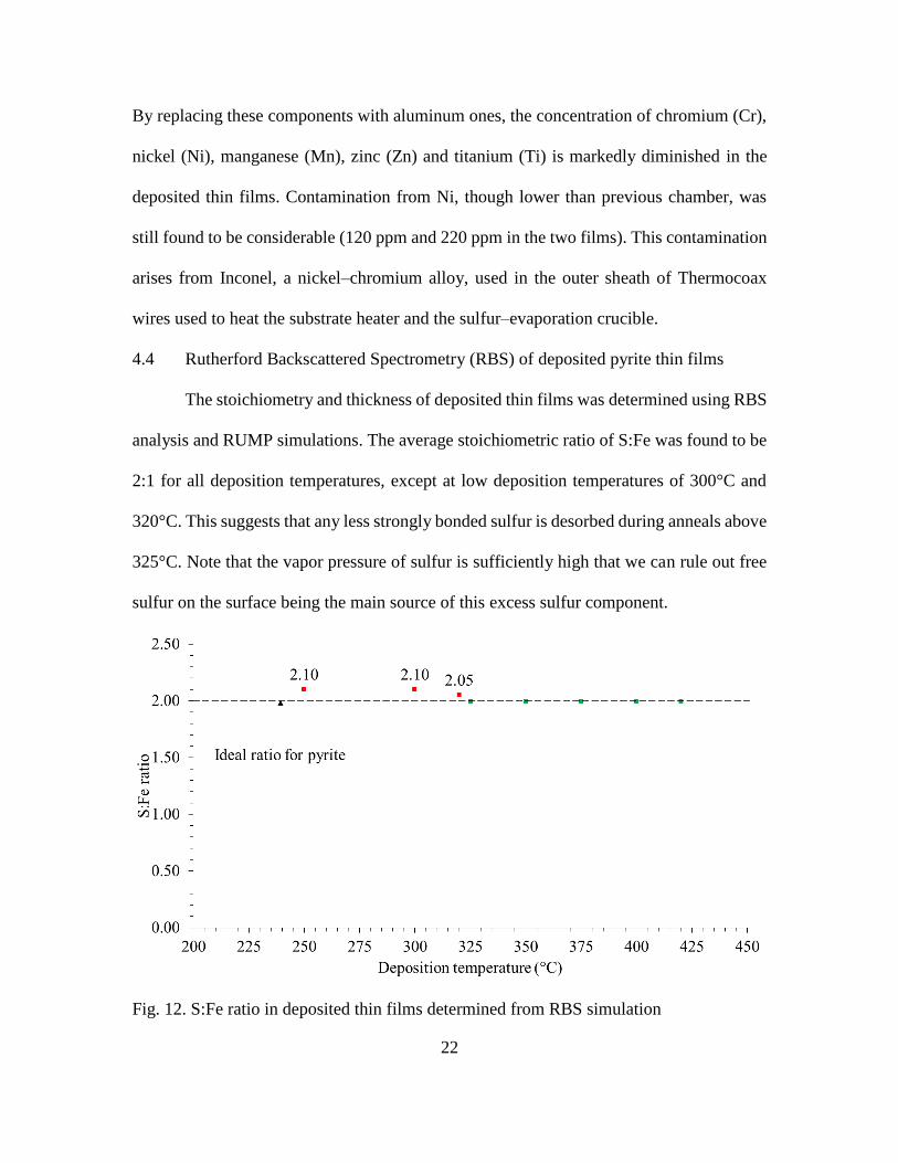
4.4 Rutherford Backscattered Spectrometry (RBS) of deposited pyrite thin films
The stoichiometry and thickness of deposited thin films was determined using RBS
analysis and RUMP simulations. The average stoichiometric ratio of S:Fe was found to be
2:1 for all deposition temperatures, except at low deposition temperatures of 300°C and
320°C. This suggests that any less strongly bonded sulfur is desorbed during anneals above
325°C. Note that the vapor pressure of sulfur is sufficiently high that we can rule out free
sulfur on the surface being the main source of this excess sulfur component.
Fig. 12. S:Fe ratio in deposited thin films determined from RBS simulation
23
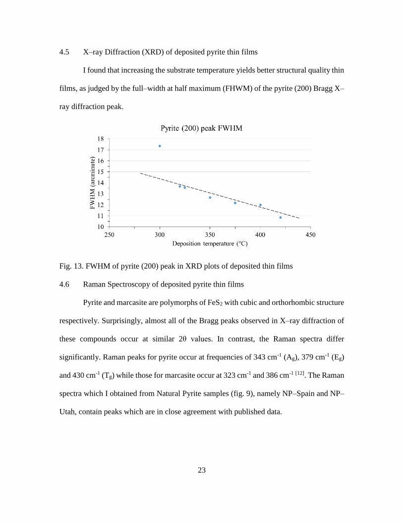
4.5 X–ray Diffraction (XRD) of deposited pyrite thin films
I found that increasing the substrate temperature yields better structural quality thin
films, as judged by the full–width at half maximum (FHWM) of the pyrite (200) Bragg X–
ray diffraction peak.
Fig. 13. FWHM of pyrite (200) peak in XRD plots of deposited thin films
4.6 Raman Spectroscopy of deposited pyrite thin films
Pyrite and marcasite are polymorphs of FeS2 with cubic and orthorhombic structure
respectively. Surprisingly, almost all of the Bragg peaks observed in X–ray diffraction of
these compounds occur at similar 2θ values. In contrast, the Raman spectra differ
significantly. Raman peaks for pyrite occur at frequencies of 343 cm-1 (Ag), 379 cm-1 (Eg)
and 430 cm-1 (Tg) while those for marcasite occur at 323 cm-1 and 386 cm-1 [12]. The Raman
spectra which I obtained from Natural Pyrite samples (fig. 9), namely NP–Spain and NP–
Utah, contain peaks which are in close agreement with published data.

24
Fig. 14. Raman spectra from iron sulfides obtained using green (523 nm) excitation [12]
Fig. 15. Raman spectra obtained from natural pyrite samples
(Grey: NP–Spain; Blue and Orange: NP–Utah)
By performing Raman spectroscopy measurements on deposited thin films, I was
able to distinguish between pyrite and marcasite thin films. I also quantified the relative
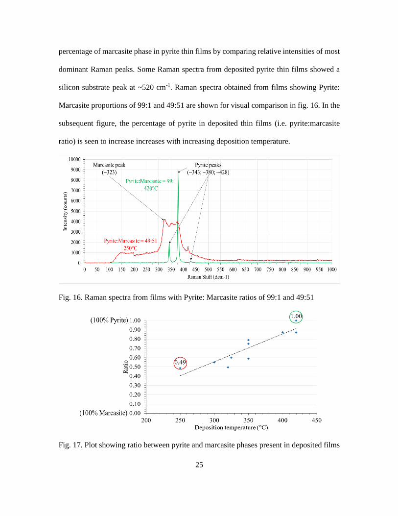
25
percentage of marcasite phase in pyrite thin films by comparing relative intensities of most
dominant Raman peaks. Some Raman spectra from deposited pyrite thin films showed a
silicon substrate peak at ~520 cm-1. Raman spectra obtained from films showing Pyrite:
Marcasite proportions of 99:1 and 49:51 are shown for visual comparison in fig. 16. In the
subsequent figure, the percentage of pyrite in deposited thin films (i.e. pyrite:marcasite
ratio) is seen to increase increases with increasing deposition temperature.
Fig. 16. Raman spectra from films with Pyrite: Marcasite ratios of 99:1 and 49:51
Fig. 17. Plot showing ratio between pyrite and marcasite phases present in deposited films

26
4.7 Optical topography of deposited pyrite thin films
The optical topography of the pyrite thin films deposited in the upgraded chamber
was characterized using an optical profilometer (Zemetrics, Model ZeScope, at LeRoy
Eyring Center for Solid State Science) with a depth resolution better than 1 Å. The figure
below shows that the average roughness decreases with increasing deposition temperature.
This can be attributed to improved diffusion and mass transport at elevated temperatures
on the growth surface.
Fig. 18. Plot showing relation between optical roughness of deposited thin films and
deposition temperature
4.8 UV/Vis/Near–IR spectroscopy of deposited pyrite thin films
Transmission and reflection measurements were performed on pyrite thin films
deposited in the upgraded chamber using a spectrophotometer (PerkinElmer, Model
Lambda 950 S with Automated Reflectance/Transmittance Analyzer (ARTA) accessory).
The range of spectrum analyzed during measurements is 250 nm (4.96 eV) to 2000 nm
(0.62 eV). The optics configuration of this tool is shown in the figure below. The substrate
27
is positioned at an angle of 10° with respect to incident beam. The angle between incident
and transmitted beam is 180°, while that between incident beam and reflected beam is 20°.
Fig. 19. Schematic diagrams showing optics arrangement in (a) transmission mode; (b)
reflection mode
Fig. 20. Arrangement of optics in ARTA accessory during transmission measurements
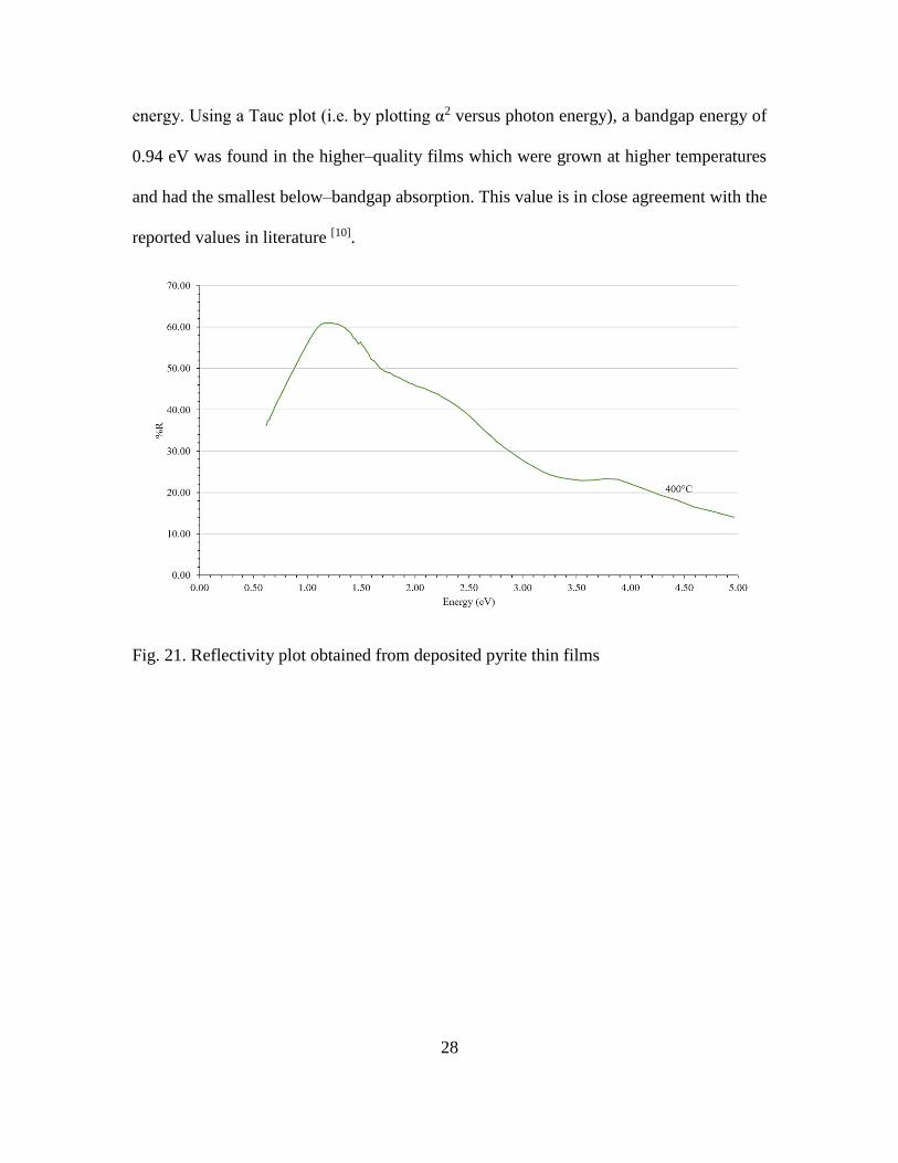
The pyrite bandgap based on optical measurements has been reported to be 0.9 eV
[10]. Fig. 11 shows the reflectivity data measured from pyrite thin films deposited in the
upgraded chamber. The peak around 1.5 eV is attributed to 3d intraband transitions from
3d t2g into the antibonding eg* state and the second peak at ~ 4.0 eV has been attributed to
interband transitions from S 3p band into the Fe 3d eg* state [11]. The discontinuity in data
points at ~1.48 eV in all the plots is due to an instrumental change in detector optics at this
28
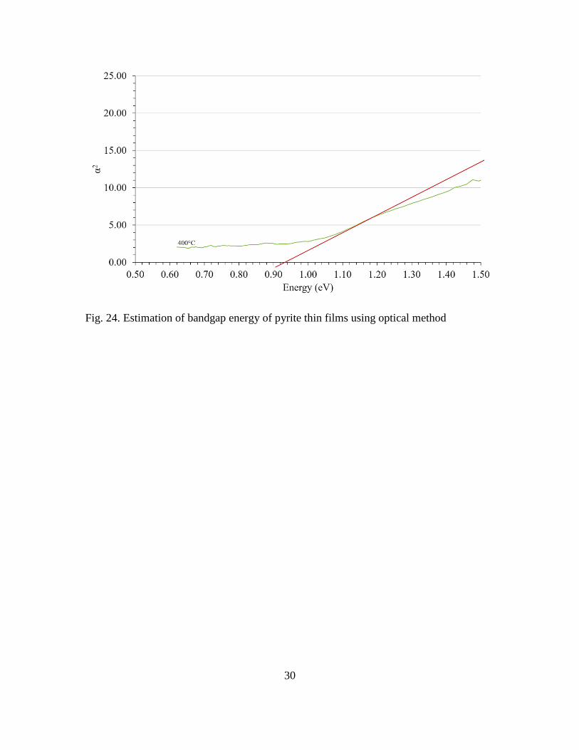
energy. Using a Tauc plot (i.e. by plotting α2 versus photon energy), a bandgap energy of
0.94 eV was found in the higher–quality films which were grown at higher temperatures
and had the smallest below–bandgap absorption. This value is in close agreement with the
reported values in literature [10].
Fig. 21. Reflectivity plot obtained from deposited pyrite thin films

29
Fig. 22. Transmission data obtained from deposited pyrite thin films
Fig. 23. Variation in absorption coefficient with increasing photon energy
30
Fig. 24. Estimation of bandgap energy of pyrite thin films using optical method

31
CHAPTER 5
CONCLUSIONS
Using a systematic material selection process, I designed, built and used a
sequential–evaporation growth system to improve the structural quality, surface
smoothness, chemical stoichiometry and phase purity of pyrite thin films.
Stoichiometric pyrite thin films were obtained at all temperatures above 325°C. The
smoothness of films, as measured by optical profilometer, and crystal quality, as judged by
FWHM of X–ray diffraction pyrite (200) Bragg peak, improved with increasing deposition
temperature up to highest temperature used, i.e. 420°C. The percentage of pyrite phase in
the deposited thin films, as determined from Raman spectra, also increased with increasing
deposition temperature up to a value of 100% at 420°C. SIMS measurements from thin
films deposited in the upgraded chamber, with mostly Al parts, have contamination levels
3 orders of magnitude smaller than those found for the older chamber, with mostly stainless
steel and copper parts. Contamination from some elements such as bromine (Br), lead (Pb)
and molybdenum (Mo) has been completely eliminated.
Using a Tauc plot, I measured the bandgap energy of highest–quality pyrite thin
films deposited using my chamber to be 0.94 eV.

32
CHAPTER 6
FUTURE WORK
In order to further reduce impurity concentrations in the deposited pyrite thin films,
it is necessary to identify the source of the remaining contaminants. For example, nickel
(Ni) is present in the Inconel alloy covering the Thermocoax heating elements. Alternative
materials should be sought in order to completely eliminate sources of nickel
contamination. An iron heating element might also be considered. A ceramic covering
should also be used to cover the wiring, especially where the element enters the heater,
since they are not thermally anchored and are thus at a much higher temperature than the
rest of the wiring. A thorough study to determine the mean time to failure should be
performed.
It was noted that crystal quality and phase purity of pyrite thin films improves with
increasing deposition temperature. In order to attain higher deposition temperatures, up to
530°C for 1 Torr sulfur pressure, I would suggest that the aluminum bottom–plate and
bottom–disc should be replaced with more heat–resistant materials, like Macor ceramics.
Having optimized the chamber for high–structural quality pyrite thin film deposition,
doping with donors dopants and acceptor dopants to form n– and p–type pyrite,
respectively, can be considered as the next objective. The upgraded chamber built during
this project is capable of incorporating an additional evaporation source on the bottom
flange.

33
CHAPTER 7
REFERENCES
1. W. Shockley and H. J. Queisser, “Detailed Balance Limit of Efficiency of p–n Junction
Solar Cells”, Journal of Applied Physics 32 (1960): pp. 510–519
2. Martin A. Green, Keith Emery, Yoshihiro Hishikawa, Wilhelm Warta and Ewan D.
Dunlop, “Solar cell efficiency tables (Version 45)”, Progress in Photovoltaics:
Research and Applications 23 (2015): pp. 1–9
3. C. Wadia, A. P. Alivisatos and D. M. Kammen, “Materials Availability Expands the
Opportunity for Large–Scale Photovoltaics Deployment”, Environmental Science &
Technology 43 (2009): pp. 2072–2077
4. P. S. Vasekar and T. P. Dhakal, Thin Film Solar Cells Using Earth–Abundant
Materials, Solar Cells – Research and Application Perspectives, (InTech, 2013, ISBN:
978-953-51-1003-3): pp. 145–168
5. ASM Handbook 3, (ASM International, Ed. Hugh Baker, Materials Park, Ohio, 1992)
6. M. Vahidi, S. W. Lehner, P. R. Buseck and N. Newman, “Growth of epitaxial pyrite
(FeS2) thin films using sequential evaporation”, Acta Materialia 61 (2013): pp. 7392–
7398
7. A. Wertheim, “Growth and Characterization of Pyrite thin films for photovoltaic
applications, A thesis submitted in partial fulfillment of the requirements for the degree
Masters of Science”, (2014): pp. 24–27
8. H. J. T. Ellingham, “Reducibility of Oxides and Sulphides in Metallurgical Processes,”
Journal of the Society of Chemical Industry 63 (1944): pp. 125–133
9. Y. Alaskar, S. Arafin, Q. Lin, D. Wickramaratne, J. McKay, A. G. Norman, Z. Zhang,
L. Yao, F. Ding, J. Zou, M. S. Goorsky, R. K. Lake, M. A. Zurbuchen and K. L. Wang,
“Theoretical and experimental study of highly textured GaAs on silicon using a
graphene buffer layer”, Journal of Crystal Growth 425 (2015): p. 271
10. A. Schlegel and P. Wachter, “Optical properties, phonons and electronic structure of
iron pyrite (FeS2)”, Journal of Physics C: Solid State Physics 9 (1976): pp. 3363–3369
11. I. J. Ferrer, D. M. Nevskaia, C. de las Heras and C. Sánchez, “About the band gap
nature of FeS2 as determined from optical and photo–electrochemical measurements”,
Solid State Communications 74 (1990): pp. 913–916

34
12. S. N. White, “Laser Raman spectroscopy as a technique for identification of seafloor
hydrothermal and cold seep minerals”, Chemical Geology 259 (2009): pp. 240–252
13. S. W. Lehner, N. Newman, M. van Schilfgaarde, S. Bandyopadhyay, K. Savage and P.
R. Buseck, “Defect energy levels and electronic behavior of Ni–, Co–, and As–doped
synthetic pyrite (FeS2)”, Journal of Applied Physics 111 (2012): p. 083717-7


![Ti and Ni - Oxidation Paper - REVISED · 2013-05-21 · [22] added a nomographic scale to the Ellingham diagram. The Ellingham-Richardson diagram for a series of oxides is shown in](https://static.fdocuments.in/doc/165x107/5f0fe5457e708231d4466bdd/ti-and-ni-oxidation-paper-revised-2013-05-21-22-added-a-nomographic-scale.jpg)