
Design of a Dual Band GaN PA Utilizing Dual Band Impedance ...
34
APPROVED: Hyoung Soo Kim, Major Professor Hualiang Zhang, Committee Member Shengli Fu, Committee Member and Interim Chair of the Department of Electrical Engineering Costas Tsatsoulis, Dean of the College of Engineering Mark Wardell, Dean of the Toulouse Graduate School DESIGN OF A DUAL BAND GaN PA UTILIZING DUAL BAND IMPEDANCE TRANSFORMERS David R. Poe Thesis Prepared for the Degree of MASTER OF SCIENCE UNIVERSITY OF NORTH TEXAS May 2013
Transcript of Design of a Dual Band GaN PA Utilizing Dual Band Impedance ...
APPROVED:
Hyoung Soo Kim, Major Professor Hualiang Zhang, Committee Member Shengli Fu, Committee Member and Interim
Chair of the Department of Electrical Engineering
Costas Tsatsoulis, Dean of the College of Engineering
Mark Wardell, Dean of the Toulouse Graduate School
DESIGN OF A DUAL BAND GaN PA UTILIZING DUAL BAND IMPEDANCE TRANSFORMERS
David R. Poe
Thesis Prepared for the Degree of
MASTER OF SCIENCE
UNIVERSITY OF NORTH TEXAS
May 2013

Poe, David R. Design of a Dual Band GaN PA Utilizing Dual Band Impedance
Transformers. Master of Science (Electrical Engineering), May 2013, 30 pp., 12
figures, references, 14 titles.
This thesis discusses the design, fabrication, and testing of a high efficiency, dual band
radio frequency power amplifier. While it is difficult to demonstrate an exact mode of
operation for power amplifiers at radio frequencies, based on the characteristics of the
transistor itself, the argument can be made that our high efficiency performance is due to an
approximation to class E operation. The PA is designed around a CGH40025 transistor
manufactured by Cree, Inc, which has developed a very useful nonlinear model of its transistor,
which allows use of software load/source pull methods to determine optimum impedances to
be presented to the gate and drain (hereafter referred to as source and load) of the transistor
at each band of operation. A recent work on dual-band impedance matching is then used to
design distributed element networks in order to present conjugate matches of these
impedances to the transistor. This is followed by a careful layout, after which the PA is then
fabricated on a low-impedance substrate using a LPKF Protomat S63 rapid prototyping
machine. Measurements of gain and drain current provide values for power-added-efficiency.
Simulated gains were 21 and 18 dB at 800 MHz and 1.85 GHz, respectively, with PAE around
63% for both bands. Measurements taken from the fabricated PA showed gains of 20 and 16 dB
at each band, but PAE of 80% at 800 MHz and 43% at 1.85 GHz.

Copyright 2013
by
David R. Poe
ii

TABLE OF CONTENTS
Page
Chapters
1. INTRODUCTION TO RADIO FREQUENCY POWER AMPLIFIER DESIGN ............................ 1
2. RESEARCH BACKGROUND ............................................................................................. 11
3. APPLICATION OF RESEARCH BACKGROUND TO DESIGN PROBLEM ............................. 16
4. LAYOUT AND FABRICATION OF THE POWER AMPLIFIER .............................................. 23
5. MEASUREMENT OF FABRICATED POWER AMPLIFIER AND RESULTS ........................... 26
REFERENCES .................................................................................................................................. 30
iii

CHAPTER 1
INTRODUCTION TO RADIO FREQUENCY POWER AMPLIFIER DESIGN
1.1 General Power Amplifier Design
The heart of any modern amplifier design is the transistor. Transistors used in radio
frequency (RF) applications require more careful design, specialized materials and packages,
and smaller feature sizes than lower frequency applications; these efforts to minimize feature
sizes are necessary to minimize parasitic reactances and allow meaningful RF operation, but
substantially increase the cost of such transistors. RF bipolar junction transistors (BJTs) came
before RF metal-oxide-semiconductor field-effect transistors (MOSFETS); at lower frequencies
the high input impedance to the MOSFET gives it an advantage in that it is easier to match, but
as parasitics take their toll above 800 MHz this advantage disappears [1]. In general, MOSFETs
suffer from lower transconductance than BJTs for a given current; however, special design
methods yielding high-electron-mobility transistors (HEMTs), a form of FET, yield better
transconductances than BJTs. An example of a HEMT would be the CGH40025F, the transistor
utilized in this design [2].
Power amplifier (PA) designs can incorporate a single or multiple transistors; multiple
transistor designs can be divided into parallel and push-pull topologies. Parallel designs are
used when they would give an overall advantage in power output than using a single transistor
alone; BJTs used for this purpose usually require intermediate impedance transformers at their
inputs to prevent the parallel combination of input resistances from causing the overall input
impedance from becoming too small. A naive understanding of this issue would suggest that
1
the extremely high input impedances of MOSFETS would make them ideal for parallel
topologies; alas, the inductances resulting from packages and capacitance from the internal
structures of MOSFETs conspire to make oscillators out of two devices in parallel. Careful
isolation strategies must be employed to avoid this device damaging phenomenon, which limit
the usefulness of these transistors in parallel configurations. Push-pull configurations, where
two transistors conduct for half of the input cycle, can eliminate production of even harmonics,
but require careful matching, especially at higher frequencies [1].
Taken with a host of idealizations, we may divide general amplifier design into two
broad categories: conventional conduction-mode [3] (also called transconductance [4])
amplifiers, which amplify a signal by varying the current through a transistor with an input
voltage, and switch-mode amplifiers, which operate transistors as switches with nearly
instantaneous voltage switching between saturation and cutoff and use specialized output
networks to pass only the fundamental frequency to the load; we may also remark that
transconductance amplifiers have the theoretical possibility of perfect linearity, while at least
two classes of switch-mode operation are theoretically perfectly efficient.
1.2 Conventional Conduction Modes
Transconductance amplifiers may be subdivided into four classes of operation, based
upon the “conduction angle” of the circuit in question. The conduction angle of an amplifier is
the angle, out of the full cycle of 2π, of an input sinusoid for which a transistor is conducting;
for example, for a transistor with Vt = 1.0 V, a direct current (DC) gate bias of 2 V and a 2V peak-
to-peak alternating current (AC) signal will result in a conduction angle of 2π, while the same AC
signal applied to the input of the same transistor with a DC gate bias of 1 V will result in a
2

conduction angle of π. As the maximum input voltage is restricted by the IMAX of the device, the
conduction angle and therefore the class of operation for transconductance amplifiers will be
given primarily by the DC gate bias VG. Class A amplifiers have θC = 2π and conduct over the full
input cycle while class B amplifiers have θC = π and conduct only exactly half the input cycle.
Class AB amplifiers, as the name implies, conduct for an angle π < θC < 2π; class C amplifiers
conduct for any θC < π.
Presuming perfect linear transconductance of the transistor, two important attributes
arise from analysis of the effects of “clipping” the output current waveform in such a manner.
Lowering the bias voltage and so reducing the conduction angle results in less current drawn
through the transistor for a given AC input voltage; Fourier analysis of this current reveals that
the DC component of the current waveform falls below the fundamental harmonic component
as the conduction angle is decreased, resulting in increased DC-to-AC efficiency, the primary
draw of reducing the conduction angle. However, Fourier analysis also reveals the drawback to
increasing efficiency in such a manner: generation of higher-order transistor current harmonics
of the fundamental input voltage. In ideal analyses, a parallel LC tank across the load at the
design frequency can be used to short these harmonics to ground, preventing a voltage drop
across the load at these harmonics and ensuring no AC power is generated at these
frequencies; however, the decreasing amounts of fundamental current for a given AC input
voltage still effects the linearity of the amplifier [3].
In the absence of perfect linear transconductance, however, even class A amplifiers are
not perfectly linear; by linearity, we mean “a measure of how closely the output signal of the
amplifier resembles the input signal” [5:155]. When the output voltage can be expressed as a
3

constant multiplied by the input voltage, we have perfect linearity; when this equation has
higher order polynomials of input voltage, trigonometry results in the production of higher-
order harmonics in the output current. In practice, perfect harmonic shorts are not available,
inevitably resulting in some power production at the higher order harmonics of the input
fundamental frequency whenever harmonic current is produced, whether by transconductance
or bias point [3],[5].
1.3 Switch-Mode Amplifiers
Sharing a common topology, ideal transconductance amplifiers present different output
current harmonics based on the input bias voltage. For switch-mode amplifiers, bias voltage is
irrelevant – the transistor is operated as a switch which ideally transitions instantaneously
between open and closed; for voltage controlled transistors, this implies square-wave voltage
inputs. Contrary to intuition, this does not result in a square wave of current at the output;
switch-mode amplifiers use a resonator circuit at the output to force sinusoidal current through
the load, which results in sinusoidal current through the transistor when in conduction and
highly irregular voltage waveforms across the transistor. Accordingly, the topologies of
different classes of operation for switch mode operation vary substantially, though many share
output series LC resonators at the design frequency. Class F amplifiers arise from consideration
of “overdriven” Class A and Class AB amplifiers and makes use of a similar topology, but with a
series resonator through the load. Class D amplifiers use a pair of transistors, in series between
VDD and ground, with the output taken at the source of the “upper” transistor and drain of the
“lower” transistor; each conducts one half of a sinusoidal load current through an output series
resonator. Class E amplifiers use a single transistor in parallel with a shunt capacitance, again
4
with a series output resonator. Class F and variants are theoretically capable of around 90%
maximum efficiency, while Class D and E are both theoretically capable of 100% efficiency.
As the design methodology presented in this thesis is based on achieving RF class E
operation, both by exploiting properties inherent to the chosen transistor as well as design of
matching networks that have similar properties to a broadband Class E work using the same
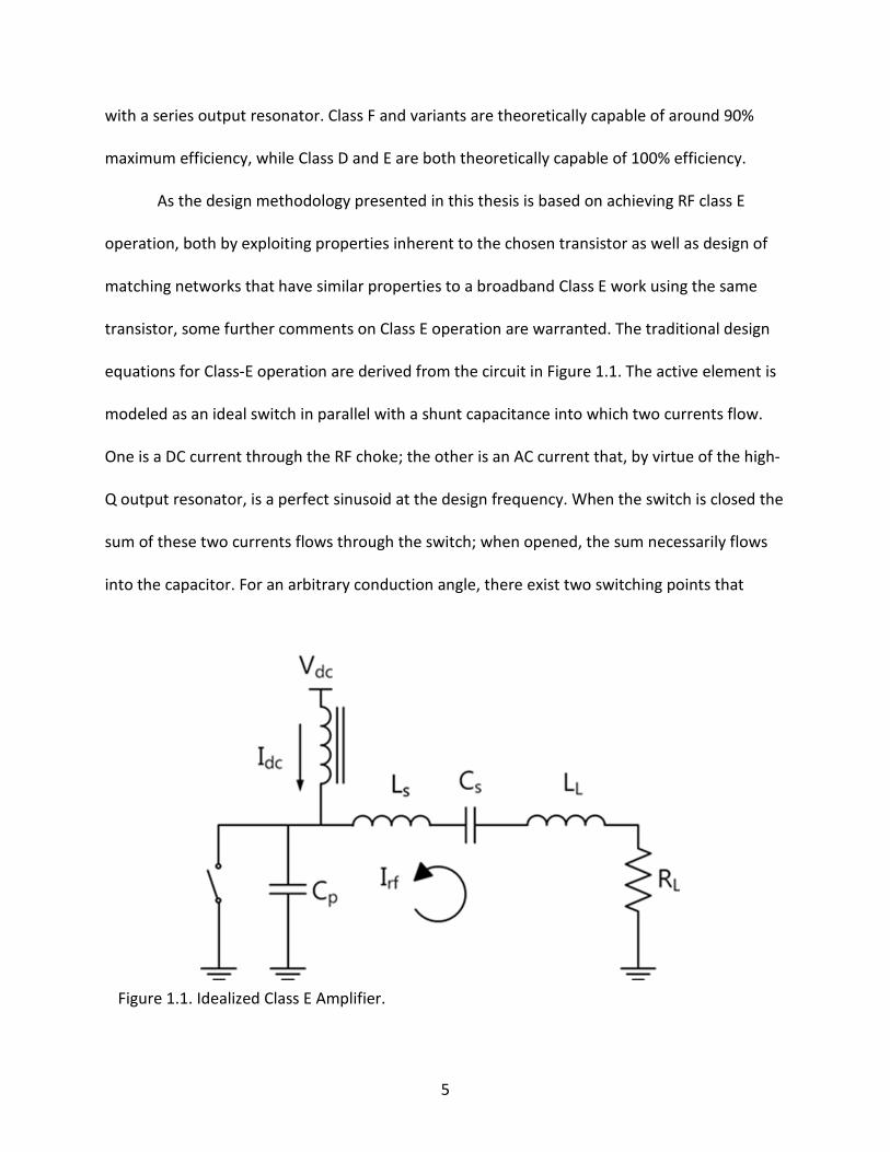
transistor, some further comments on Class E operation are warranted. The traditional design
equations for Class-E operation are derived from the circuit in Figure 1.1. The active element is
modeled as an ideal switch in parallel with a shunt capacitance into which two currents flow.
One is a DC current through the RF choke; the other is an AC current that, by virtue of the high-
Q output resonator, is a perfect sinusoid at the design frequency. When the switch is closed the
sum of these two currents flows through the switch; when opened, the sum necessarily flows
into the capacitor. For an arbitrary conduction angle, there exist two switching points that
Figure 1.1. Idealized Class E Amplifier.
5

guarantee the switch will not close while there is current through or net charge on the
capacitor, preventing switching losses. While the switch is open, the current through the
capacitor results in a voltage waveform across the capacitor; Fourier analysis of this voltage
reveals both in-phase and quadrature components (as compared to the current waveform) at
the design frequency. The quadrature voltage component results in a need for a slightly
reactive load; the in-phase component together with the current waveform produces power at
the fundamental frequency. This power is precisely equal to the DC power dissipated by the
voltage and current supplies, revealing the draw of ideal class E operation: theoretically perfect
conversion of DC to RF power [3].
1.4 Realities at GHz and beyond
As mentioned, the preceding analyses make many ideal assumptions that will not hold
up to practical implementation. A glaring impossibility is the use of ideal LC resonators, either in
series or parallel, to prevent higher-order harmonic current from flowing through the load
resistor; at RF frequencies, discrete lumped components have parasitic Q-factors and raise the
specter of self-resonant components. Distributed elements must be substituted instead, with a
concomitant increase in impedance calculation complexity. Classical conduction mode analyses
presume a linear transconductance characteristic; while class A is ideally perfectly linear,
modulated input signals combined with a realistic transconductance characteristics can
produce nasty surprises [3]. An issue facing both categories of amplifier is the host of parasitics
associated with any real transistor, which make analytical treatment of the above equivalent
circuits all but intractable.
6

Switch mode operation, in particular, is compromised by its fundamental assumption –
square wave voltage inputs. A square wave has an infinite set of harmonic components, each of
which will be presented with a different impedance, with the result that the GHz square wave
that enters the gate of a transistor will not be the waveform presented to the transconductive
element; any approximation to a square wave input would require an accurate matching
networks and preamplifiers with bandwidth of at least several octaves. Accordingly, switch
mode power amplifiers at RF frequencies make do with primarily fundamental frequency
inputs; switching operation is approximated by using large input signals to sweep through the
unsaturated region of the transconductance curve as quickly as possible [6].
In addition, the necessary reactive load impedance for a given frequency, determined
before using the Fourier analysis on an ideal network, has no doubt changed substantially with
the replacement of the ideal switch with a realistic transistor equivalent circuit. Deriving
analytical equations for the optimal impedance under these conditions would be quite a feat of
algebra; in our case, the capacitive parasitics of the CGH40025F are also voltage dependent [7],
so that determining the impedances would be quite a feat of differential calculus. Instead, we
will need to rely on an empirical method to determine the optimal impedances.
1.5 Load and Source Pulls
A load pull of a power amplifier setup can be succinctly described as a plot of some
metric of note over a sweep of the load network’s gamma plane. That is, the impedance
presented to the load at a given frequency is varied, with the limits of the sweep determined by
section of the gamma plane to be swept. Typical metrics are power-added-efficiency (PAE) and
output power; load pull plots highlight a maximum PAE and Pout, as well as concentric contours
7

around these maxima that correspond to backoffs from these best case results. A source pull is
such a procedure applied to the input network of the transistor.
As an empirical design method, load pulls have their origin in physical test benches with
tunable impedances, resulting in an unimpeachable set of test data; only recently have
nonlinear CAD simulations and transistor models progressed to the point where computer
simulations can provide similarly useful results. [3] This is fortunate, as load and source pull
simulations form the foundation of our design methodology. Moreover, while constructing a
physical test bench capable of varying the impedances presented to multiple harmonics at the
same time promises to be a complicated and expensive affair [8], computer simulations reduce
such a task to proper setup of such a simulation.
1.6 Stability Networks
It was mentioned earlier that parallel combinations of RF MOSFETS could easily oscillate,
limiting their usefulness in that configuration. However, given the correct conditions, single
transistors can have oscillatory instabilities as well, resulting in damage to a frequently
expensive device. This is a result of feedback capacitance between the drain and gate of the
device interacting with other parasitic inductances and capacitances within the circuit and the
transconductance gain element of the transistor, producing a negative resistance [3] .
There are a couple of metrics that allow the PA designer to guarantee that this negative
resistance will not present itself. The first, the Rollett stability factor K, is a function of the small
signal parameters of the circuit and is given by
𝐾 = 1 + |𝑠11𝑠22 − 𝑠12𝑠21|2 − |𝑠11|2 − |𝑠22|2
2|𝑠21||𝑠21|
8

For K greater than one for all frequencies, the amplifier is unconditionally stable – oscillations
will not occur for any source or load impedances. If K does not meet this criterion, oscillations
are possible, but not guaranteed and can be avoided with careful design [2].
While the Rollett stability factor can help avoid oscillations in a given design, it tells us
nothing about the relative stability of one amplifier circuit to another one. To address this,
another stability test, called the µ-factor, was derived, given by
µ = 1 − |𝑠11|2
|𝑠22 − (𝑠11𝑠22 − 𝑠12𝑠21) 𝑠11∗ | + |𝑠12𝑠21|
The µ-factor has the same requirement for stability as K, with the added bonus that larger
values of µ correspond to a larger degree of stability [9].
As mentioned, the source of low frequency instabilities is the negative resistance
resulting from the interplay of complex parasitic impedances with the gain characteristic of the
amplifier. Accordingly, addition of positive resistances to the circuit at frequencies likely to
oscillate (typically the tens of MHz range) will restore stability; however, this resistance will
harm the gain and efficiency if it is present at the frequencies to be amplified. Our stability
circuit consists of two sections – a series resistance after the RF choke inductor on the input
bias line and a resistor and a very low capacitor in parallel between the input bias network and
the gate of the transistor. The former structure adds impedance at low frequencies to the bias
line; the latter structure forces low-frequency currents to attenuate through the resistor (as the
low-valued capacitor presents a high impedance) while at high frequencies the parallel
combination of the two components results in a low-impedance path.
9

1.7 Recent Dual band Class E Amplifier Results
Interestingly, most of the recent dual band class E publications have been implemented
in CMOS. In 2012, Zhang published a design featuring concurrent class E operation at 1 – 1.3
GHz and 2.8 – 3.1 GHz, with PAE values greater than 50.5% and 30% at each band, respectively
[10]. Also in 2012, Kalim published a 130nm dual band class E amplifier utilizing compact
multiharmonic load transformation networks, arriving at 57% PAE at both 1.7 GHz and 2.5 GHz
[11]. In late 2012, Yi-Chieh Lin published a design methodology for dual band class E PAs by
optimizing circuit parameters for input power levels, achieving 65.6% and 63.6% PAE at 1.95
GHz and 2.6 GHz, respectively [12]. Most recently, in 2013 Hyuk Su Son published a fully
integrated CMOS PA to work with WCDMA and WiMAX bands, achieving 37% and 31.6% PAE at
the same bands as Lin’s work [13].
10

CHAPTER 2
RESEARCH BACKGROUND
2.1 Broadband Class E GaN-based Power Amplifier: Kenle Chen’s Paper
The foundation of our class E design methodology rests on a recent work [6] by Kenle
Chen and Dmitrios Peroulis of Purdue University, in which the design methodology for a
broadband class E amplifier is presented. Chen uses the Cree CGH40025F as well, using both
information published by Cree and a technique for estimating field-effect transistor (FET)
parasitics to come up with a relatively accurate equivalent circuit. He uses this information to
plot the ideal class-E impedances (as measured from a bare die) on the Smith chart, which he
compares with optimal impedances presented to the packaged device obtained by performing
load pull simulations on the Cree’s nonlinear model of the transistor.
In ideal class E operation, the series LC resonator would provide the necessary infinite
impedance at frequency harmonics, a luxury Chen does not have because of both the
narrowband response and the parasitics presented by such a lumped element resonator.
However, citing results showing that, in practical class E implementations, the impedance
presented to the second harmonic plays the biggest role in achieving class E efficiencies, he
works to ensure that his matching network present appropriate impedances to the 2nd and 3rd
harmonics across the frequency band. Specifically, load pull simulations are performed for
these harmonics, granting a contour set showing efficiency losses for all possible harmonic
impedance locations on the Smith chart.
11

To realize these impedance requirements, Chen combines the impedance match and
the output resonator into one structure, a distributed element realization of a real-to-real
Chebyshev low-pass matching network, using published values. While the impedance to be
matched varies with frequency, the real part hovers around 10 Ohms; the load network is
accordingly implemented as a 5:1 6th order low-pass matching network, which is then manually
tuned to tightly constrict the Smith chart plot of the network’s input impedance over the
operating band to the area about the optimal load impedances determined from the load pull
simulations. The plot also verifies that 2nd and 3rd harmonic impedances are confined to the
regions of high efficiency operation determined from the harmonic simulations. The input
matching network is designed similarly, though without consideration of harmonic impedances
and with a 20:1 transformation ratio to properly match the much lower optimum source
impedances to the system impedance.
The results are state of the art: greater than 80% drain efficiency across a 50%
bandwidth about 1.6 GHz and bandwidth of 84% with acceptable operation. The major
limitation of the setup, however, is that for optimum class E operation the bandwidth is
restricted to one octave; above an octave, the second harmonics of the lowest fundamental will
appear in the passband of the low pass filter. If one could create an impedance transformer
that could satisfy the above impedance requirements at two frequencies, then such a matching
network could produce a dual band class E power amplifier (PA).
12

2.2 Dual Band Impedance Transformers
Fortunately, a recent work [14] by Ming-Lin Chuang of National Penghu University in
Taiwan illuminates the way forward from here. Chuang’s work uses four sections of
transmission line to match two complex impedances at two uncorrelated frequencies to a
system impedance. There are two possible topologies for these four sections, utilizing two
sections in series facing the loads to be matched which are then shunted with two sections
ending in a stub or stubs, which may be open or shorted. The topologies vary on the
configuration of the stub sections – one uses two sections in series facing the open/short at the
far end of the original two section; the other has a short/open stub section facing opposite
directions at the same location. We use the former topology, shown above in Figure 2.
As Chuang notes, matching the four elements of the two arbitrary complex impedances
require four adjustable parameters in the transmission line sections; we have eight total
Figure 2. Chuang’s two-section shunt stub topology, used to match impedances at the two bands of operation.
13

parameters from these four sections. He chooses to solve the relevant equations for the
electrical lengths of the transmission lines, leaving their characteristic impedances as arbitrary
(though computationally relevant) parameters. The solution begins with the equation for the
input impedance of a transmission line. The input impedance for the first section A is given by
𝑍𝑖𝑛,𝑎 = 𝑍𝑎𝑍𝐿 + 𝑗 𝑍𝑎 tan𝛽𝑙𝑎𝑍𝑎 + 𝑗 𝑍𝐿 tan𝛽𝑙𝑎
,
where Za is the characteristic impedance of section A, ZL is the load impedance to be matched,
𝑙𝑎 is the physical length and β is the propagation constant 2 𝜋λ
at a given frequency. Section A
cascades into Section B, whose input impedance is, naturally enough,
𝑍𝑖𝑛,𝑏 = 𝑍𝑏𝑍𝑖𝑛,𝑎 + 𝑗 𝑍𝑏 tan𝛽𝑙𝑏𝑍𝑏 + 𝑗 𝑍𝑖𝑛,𝑎 tan𝛽𝑙𝑏
= 𝑍𝑏𝑍𝑎𝑍𝐿 + 𝑗 𝑍𝑎 tan𝛽𝑙𝑎𝑍𝑎 + 𝑗 𝑍𝐿 tan𝛽𝑙𝑎
+ 𝑗 𝑍𝑏 tan𝛽𝑙𝑏
𝑍𝑏 + 𝑗 𝑍𝑎𝑍𝐿 + 𝑗 𝑍𝑎 tan𝛽𝑙𝑎𝑍𝑎 + 𝑗 𝑍𝐿 tan𝛽𝑙𝑎
tan𝛽𝑙𝑏 .
This is true for both loads and frequencies. The first step in transforming the two load
impedances to match the system impedance is to find a common physical length that will
transform Zin,b at both frequencies to the form
𝑍𝑖𝑛,𝑏 = 𝑍0 + 𝑗𝑋𝑖,
where Xi will be different for the two frequencies. Chuang inverts the above expressions to
arrive at equations for the admittances Yin,b solves them with the requirement that
𝑅𝑒𝑎𝑙�𝑌𝑖𝑛,𝑏� = 𝑌0 = 1𝑍0
.
This results in in two equations that are quadratic in tan(θb) and tan(kθb), where θb is the
electrical length of section B and k is the ratio of the two frequencies. The coefficients of the
quadratic equations are themselves extremely complicated functions of θa, the characteristic
impedances of the sections Za and Zb, as well as the real and imaginary parts of the impedance
14

to be matched. Solving these two quadratic equations simultaneously results in four possible
objective equations as a function of θa. Finding a zero in any one of these equations provides
the electrical lengths of the first two sections at the first design frequency.
Once appropriate θa and θb are found, we note that since the impedance/admittance
presented by a shunt stub network is imaginary, that proper selection of the electrical lengths
θc and θd for a given set of characteristic impedances Zc and Zd will exactly cancel the
susceptances B1 and B2 presented by Yin,b, leaving Zin,b = Z0, the system impedance at both
frequencies simultaneously.
Chuang includes the equations to be solved for the initial two section segment as well as
for each of the shunt stub topologies, with the remark that one-dimensional root finding
software should be sufficient to the task. As we shall see, the reality can be more complicated
based upon the input parameters to these equations. Regardless, we now have a method to
match both of the impedances we need to construct a dual band amplifier.
15

CHAPTER 3
APPLICATION OF RESEARCH BACKGROUND TO DESIGN PROBLEM
3.1 Design Specifications and Source/Load Pulls
We chose as our design frequencies 800 MHz and 1.85 GHz, roughly corresponding to
two North American LTE bands. Cree provided the nonlinear model used by Chen, with which
we performed load pull and source pull simulations in Agilent ADS to determine optimum
impedances to present to the transistor. Agilent ADS contains stock load and source pull setups
(see Figure 3.1 below) that allow specification of harmonic impedances; these are presumed to
be 10*Z0 (500 Ohms) for higher order harmonics. This near open circuit is located on the far
right of the Smith chart and is well within the high efficiency regions for harmonic terminations
given by the contour plots in Chen’s paper; accordingly, these were left alone and repeated
iterations of source and load pull converged on optimal fundamental network impedance
values. The datasheet’s supply voltage of 28 V was used for the output DC bias, the input bias is
set at the transistor’s threshold voltage of -2.7 V, and input power is set at 30 dBm to “drive the
transistor as a switch,” as performed in Chen’s paper. The final, optimized impedance values
are
𝑍𝐿1 = 23.35 + 12.05𝑗
𝑍𝐿2 = 12.65 + 13.95𝑗
𝑍𝑆1 = 10.52 + 25.4𝑗
𝑍𝑆2 = 3.35 − 7.1𝑗
16

3.2 Impedance Transformer Calculations
These two source and two load values must now be simultaneously matched using
Chuang’s dual band impedance transformers. Two implementations of his algorithm were
created, one using MATLAB and another using Mathematica, both using the two-section series
shunt open stub topology. The MATLAB implementation is a brute force method which, for a
given set of impedances and frequencies, uses for loops to sweep through a set of realizable
values for Za, Zb, and θa and computes the four objective functions; if any are below a threshold
value, the impedances and electrical length values (a given θa that qualifies as a solution will
automatically generate a θb ) are saved for the next phase. After the full range of Za, Zb, and θa
are calculated, the a sweep of the saved values occurs, plugging them into the susceptance
equations and sweeping through the possible values for Zc, Zd, and Tc; once again, values that
cause the shunt objective equation to drop below a certain value are saved. While some
combinations of impedances and frequencies do not have any solution with physically
Figure 3.1. Stock Agilent ADS load pull setup.
17

realizable sets of characteristic impedances and electrical lengths, for those combinations that
do, many, many solutions will be generated by this method.
The Mathematica implementation of Chuang’s algorithm directly solves the objective
equation for a given set of impedances and frequencies. Counterintuitively, this is actually
much more involved than using the MATLAB script for a given amount of time per solution.
Mathematica’s root finding function requires a reasonable guess as to where a zero-crossing
happens; to provide it with such, a plot of the objective functions must be examined for zero
crossings. The situation is further complicated by the fact that a solution for a positive θa may
result in a negative θb; while merely adding λ/2 to the length will deal with that contingency for
the lower frequency, negative θb solutions are unusable for the higher frequency impedance
match. Figure 3.2 below illustrates a typical plot of the four objective functions against θa; note
Figure 3.2. A plot of the values of the four objective functions as a function of θa . Only positive, non-discontinuous zero crossings are possible, but not certain solutions to the dual band matching network.
18

that discontinuities resulting from the tangent functions inside the objective functions are not
allowed as zero-crossing solutions. One can see that for an arbitrary set of characteristic
impedances, precious few possible solutions exist, many of which are false solutions due to
their generation of a negative θb. Once acceptable θa and θb are found, solutions to θc and θd
are usually not nearly as much trouble, but the fact remains that directly solving the equations
using root finding software is only practical when searching for specific solutions; an example of
where this would be useful is in the relatively robust input network, where primary
consideration is given to minimizing electrical lengths.
As it turns out, specific solutions aren’t particularly useful in design of load networks. A
major drawback to using Chuang’s impedance transformers in PA matching network design is
that we have no control over the impedances presented to the harmonics of the design
frequencies. While all the solutions generated by the MATLAB script will match the
fundamental impedances, we will also have a galaxy of different harmonic terminations. While
drifting away from guarantees of class E operation, performing PA simulations with all of
solutions generated by the script will at least allow us to see where fortuitous combinations of
harmonic impedances grant acceptably high levels of PAE.
19

At first glance, it may seem cumbersome to simulate the over two thousand solutions
provided by the script; however, this process may be automated. Using MATLAB it is easy
enough to write the generated solutions to a text file specially formatted to be read by ADS’s
schematic capture; in particular, each set of characteristic impedances and electrical lengths is
assigned an index value. As shown above in Figure 3.3, a Data Access Component within the
ADS schematic then reads the text file and assigns appropriate values to transmission line
components in the simulation based on the index value, which is then assigned to a parameter
sweep. With the expectation that the higher frequency band will experience greater losses, we
sweep through the solution set at the higher frequency first; the solutions corresponding to the
best PAE values from this set are then simulated at the lower frequency.
Figure 3.3. Setup for mass simulations of the different electrical length and characteristic impedance values generated by the MATLAB script.
20

In addition, two port S-parameter simulations are performed, with the port facing
section A terminated in the impedance it is to match and the port facing the shunt stubs
terminated in the system impedance; a match provided by MATLAB guarantees near perfect
transmission at the design frequency, but we must also ensure that there is a large bandwidth
of transmission about the two design frequencies to guard against frequency shifts. We choose
the dual band transformer that offers the best PAE performance at both frequencies that also
meets this last criterion, using a data display like Figure 3.4 to quickly view many candidate
results at once.
Figure 3.4. Simulation results from the sweep of impedance transformers. Marker M20 highlights the maximum PAE available from this batch. On the right the width of the impedance match is displayed using S-parameters for each frequency.
21

Armed with a set of characteristic impedances and electrical lengths for the source and
load networks, we proceed to determine the physical dimensions of the microstrip lines using
ADS Linecalc. Simulations are performed comparing the S-parameter performance mentioned
in the previous paragraph for ideal lines to that presented by microstrip lines defined by lengths
and widths over a substrate; the obtained results allowed us to quickly rule out Isola substrates
as unacceptably lossy at the higher frequency. This left us with Rogers 5880LZ, also used in
Chen’s paper. In some design iterations, discrepancies existed between the ideal and substrate
simulations, which were easily tuned out to restore performance. After this step, a final PA
simulation is performed with a focus on accuracy: generic RF choke inductors are replaced with
special ADS models provided by Coilcraft, small series resistances and inductances are added to
capacitors; the results of this simulation are shown below in Figure 3.5.
Figure 3.5. Final simulation results. Clockwise from top left: S-parameters of the PA, gain at 800 MHz, PAE vs input power at 800 MHz, PAE vs input power at 1.85 GHz, gain at 1.85 GHz, and a plot of the µ factor results.
22

CHAPTER 4
LAYOUT AND FABRICATION OF THE POWER AMPLIFIER
4.1 Layout in Software
Layout of the power amplifier (PA) itself is relatively simple compared to the involved
analyses in previous steps. We place bias inputs at the top of the PA board as close as
practically possible. Both load and source matching networks shunt stubs face downward. At
appropriate distances, a ground plane on the upper surface of the PA surrounds the matching
network. Separation between ground and bias lines, as well as between distributed elements
connected through capacitors or resistors, is carefully determined for each element and ranges
from 20 mil for most of the capacitors to 100 mil for the inductors and larger values for the
stability network resistors. A rectangular hole is drawn where the transistor will rest, around
which there is a 10 mil separation between transistor and input and output lines to prevent
Figure 4.1. Layout of the PA in Agilent ADS. The rectangular hole for the transistor is shown in blue. Areas in black show where copper will be milled out of the laminate to create distributed
23

unnoticed solder spillage from shorting gate or drain to the source. Once the layout is finalized,
it is exported to Gerber layout format in preparation for fabrication.
4.2 Fabrication of Layout Using Rapid Prototyping Machine
The Gerber file is imported into the LPKF CircuitPro fabrication software. The outlines of
copper shapes are converted to polygons to prevent rubout of the interior of the transmission
lines while the hole layer specified for the transistor is moved to the Board Outline layer as part
of a method to trick the CircuitPro software into creating that necessary hole. Fiducial holes,
which allow the LPKF to reorient itself once the board is removed from the machine or flipped
over, are placed; drill holes are placed liberally about the top level ground plane, especially near
bypass capacitors, to prevent any inadvertent transmission line effects. These drill holes will be
Figure 4.2. The layout imported into LPKF's Circuit Pro software after a milling and rubout toolpaths have been generated.
24

plated using the LPKF EasyContac process. While care and experience are necessary to have
the LPKF produce proper results, automated dialogs take over production at this point,
generating toolpaths for milling, drilling, and rubout (see Figure 4.2 on the previous page)
finally the fabrication of board. An example of useful experience in this regard is the fact that if
another board outline is specified in addition to the hole the transistor will sit in, the entire
contour routing path will switch to “outside” as opposed to “inside” mode and create a much
larger hole for the transistor than is acceptable. To “contour route” the outside of the layout, a
paper slicer is used to cut the board out of the laminate. The board is then populated and ready
to be tested.
Figure 4.3. The LPKF proceeding through a "rubout" phase for a PA layout, milling away the unneeded copper laminate.
25

CHAPTER 5
MEASUREMENT OF FABRICATED POWER AMPLIFIER AND RESULTS
5.1 Measurement Setup
The testing of a power amplifier (PA) is not a task to be approached lightly. The
transistor itself is worth well over $100; the instrumentation necessary to generate the
necessary input signals and to measure the output power at that frequency are an order of
magnitude more expensive. Absent minded input network design resulting in a mismatch at the
input network or oscillations could cause reflections or generated radio frequency (RF) power
to travel towards the signal generator, damaging the equipment if it exceeds its rated
reflection-handling capability. On the output, a design that performs better than expected or is
inadvertently optimized for gain could produce sufficient power to overwhelm the power
sensor’s power handling capability. Put simply, attenuating or blocking microwave circuit
elements should be placed at the input and output of the PA under test to prevent signals
emerging from these ports from damaging the other test instrumentation.
Some attention must also be paid to the capabilities of the test equipment. For example,
the vector signal generator (VSG) in the lab is a Agilent E4438, which is only capable of
generating +20 dBm output power signals. Our simulations run up to 30 dBm and as our design
is a switch mode amplifier we need to reach these input levels to achieve the PAE characteristic
of such designs; we therefore need a preamplifier as well.
To address these concerns, isolators and preamplifiers were obtained for each
frequency band, in addition to a 30 dBm attenuator that functioned across both. The
26

preamplifiers were supplied free of charge by Hittite microwave as evaluation boards for their
HMC451 and HMC463 transistors. The power sensor used was a Rhode and Schwartz NRP-Z24;
this sensor choice reduced test setup complexity as a USB output to a PC-based power meter,
instead of requiring a separate power meter on the testbench. A diagram of the assembled
setup is shown below.
The exact value of attenuation provided by the attenuator is measured using the test
equipment. The output power of each of the preamplifiers is measured for each of the output
powers used from the VSG; as the preamplifiers are fed through the isolators for each
frequency, we eliminate calibration requirements for the isolators as we already know the
exact value of the input power presented to the PA under test for a given VSG output power
setup. We enter these values into a spreadsheet that adjusts for their effects; all that is needed
to calculate the pertinent values of PAE, output power and gain now is the supply current
through the drain bias lines and the output powers themselves.
5.2 Results
Measurements at the design frequencies failed to demonstrate the expected values of
gain and PAE; the PA was then attached to the vector network analyzer (VNA) in the lab to
Figure 5.1. Diagram of PA test setup.
27

determine s-parameters. Examination of those results showed s21 peaks at 750 MHz and 1.62
GHz, corresponding to frequency shifts of 50 MHz and 230 MHz, respectively. Measurement
resumed with the VSG generating these frequencies. At 750 MHz, a gain of 20 dB and maximum
PAE of 83% were measured; at 1.62 GHz, the gain was 16 dB and maximum PAE was 45%,
summarized in Figure 5.2 below.
While the gain values are a comfortable validation of our simulation performance, the
PAE values are puzzling – in simulation, PAE maxed out in the 60% range for both frequencies.
One interpretation of such results is that the same fabrication effects that caused the frequency
shift shifted the second and third harmonic impedances of the lower band into more favorable
regions of the Smith chart (as discussed in Chen’s paper) for class E operation, while the
opposite effect occurred for the upper band.
5.3 Future Work
The results show that class E operation is possible using Chuang’s dual band impedance
transformers, if only at one frequency. Using different supply voltages, the gains presented at
each frequency could be equalized for a commercially more practical PA.
Figure 4. Measurement results from the fabricated PA. From left: results at 750 MHz, results at 1.62 GHz, and the measured S-parameters.
28

During testing, it was shown that the input impedance of Chuang’s networks form a
spiral about the Smith chart; if Chen’s class E analysis holds true, selection of fundamental
frequencies whose S-parameter value is near the fundamental ideal for class E operation whilst
simultaneously presenting high-impedance values in the appropriate regions of the Smith chart
at the second and third harmonics should grant class E operation. Additionally, these input
impedances were only simulated for the two-series section shunted stub topology; using the
topology that uses two shunted stubs facing in opposite directions may generate an impedance
spiral that presents more favorable characteristics for achieving class E operation.
29

REFERENCES
1. N. Dye and H. Granberg. Radio Frequency Transistors: Principles and Practical Applications, 2nd ed. Boston, MA: Newnes, 2001, pp. 31-55,113-123.
2. E. da Silva. High Frequency and Microwave Engineering. Oxford: Butterworth-Heinemann. 2001, pp. 262-321.
3. S. Cripps, RF Power Amplifiers for Wireless Communications, 2nd ed. Boston, MA: Artech House, 2006, pp. 1-229.
4. M. Eron, B. Kim, F. Raab, R. Caverley, and J. Staudinger. "The Head of the Class." IEEE Microwave Magazine, vol. 12, no. 7, pp. S16-S33, Dec. 2011.
5. C. Bowick. RF Circuit Design. Indianapolis, IN: H. W. Sams, 1982, pp. 150-156.
6. K. Chen and D. Peroulis, "Design of Highly Efficient Broadband Class-E Power Amplifier Using Synthesized Low-Pass Matching Networks." IEEE Transactions on Microwave Theory and Techniques, vol. 59, no. 12, pp. 3162-3173, Dec. 2011.
7. R. Pengelly, B. Millon, D. Farrell, B. Pribble, and S. Wood, “Applications of non-linear models in a range of challenging GaN HEMT power amplifier designs,” presented at the IEEE MTT-S International Microwave Symposium Workshop, Atlanta, GA, 2008.
8. R. Larose, F. Ghannouchi, and R. Bosisio. "A new multi-harmonic load-pull method for nonlinear device characterization and modeling." IEEE MTT-S Digest, 1990, pp. 443-446.
9. D. M. Pozar, Microwave Engineering, 3rd edition. Boston, MA: Wiley, 2005.
10. R. Zhang, M. Acar, M. Apostolidou, M. Van der Heijden, D. Leenaerts. "Concurrent L- and S band class-E power amplifier in 65nm CMOS," IEEE Radio Frequency Integrated Circuits Symposium Digest, 2012, pp. 217-220.
11. D. Kalim, A. Fatemi, and R. Negra. “Dual band 1.7 GHz / 2.5 GHz class-E power amplifier in 130 nm CMOS technology." IEEE 10th International New Circuits and Systems Conference, 2012, pp. 473-476.
12. Y. Lin, C. Chen, and T. Horng. “High efficiency dual band Class-E power amplifier design.” Asia-Pacific Microwave Conference Proceedings, 2012, pp.355-357.
13. H. Son, W. Kim, J. Jang, H. Lee, I. Oh, and C. Park. “A Fully Integrated CMOS Class-E Power Amplifier for Reconfigurable Transmitters with WCDMA/WiMAX Applications," Proceedings of 26th International Conference on VLSI Design, 2013, pp.169-172.
14. M. Chuang, "Dual band Impedance Transformer Using Two-Section Shunt Stubs," IEEE Transactions on Microwave Theory and Techniques, vol.58, no.5, pp.1257-1263, May 2010.
30


![Suspended Metasurface Loaded Dual Band Dual Polarized ... › proceedings › procAP19 › papers2019 › PID5638363.pdf · filter. In [9], a dual band dual polarized antenna is](https://static.fdocuments.in/doc/165x107/5f14de5c84dbd949e06a47a4/suspended-metasurface-loaded-dual-band-dual-polarized-a-proceedings-a-procap19.jpg)

![Ultraviolet polarized light emitting and detecting dual-functioning … · 2019. 7. 14. · similar band structure between ZnO and GaN [5], p-GaN has been widely employed to fabricate](https://static.fdocuments.in/doc/165x107/60f4983f23a0ef2edd737140/ultraviolet-polarized-light-emitting-and-detecting-dual-functioning-2019-7-14.jpg)