DUAL-BAND AND SWITCHED-BAND HIGHLY EFFICIENT POWER …
169
DUAL-BAND AND SWITCHED-BAND HIGHLY EFFICIENT POWER AMPLIFIERS By Fatemeh Norouzian A thesis submitted to University of Birmingham for the degree of DOCTOR OF PHILOSOPHY School of Electronic, Electrical and Computer Engineering University of Birmingham October 2014
Transcript of DUAL-BAND AND SWITCHED-BAND HIGHLY EFFICIENT POWER …

DUAL-BAND AND SWITCHED-BAND HIGHLY EFFICIENT POWER
AMPLIFIERS
By
Fatemeh Norouzian
A thesis submitted to
University of Birmingham
for the degree of
DOCTOR OF PHILOSOPHY
School of Electronic, Electrical and Computer Engineering
University of Birmingham
October 2014

University of Birmingham Research Archive
e-theses repository This unpublished thesis/dissertation is copyright of the author and/or third parties. The intellectual property rights of the author or third parties in respect of this work are as defined by The Copyright Designs and Patents Act 1988 or as modified by any successor legislation. Any use made of information contained in this thesis/dissertation must be in accordance with that legislation and must be properly acknowledged. Further distribution or reproduction in any format is prohibited without the permission of the copyright holder.

II
Abstract The Power Amplifier is the most challenging module of a wireless network to design and
it is the highest power consumer. Lots of research has been dedicated to design highly
efficient and linear power amplifiers in the last decades. The high demand for wireless
communication systems creates the requirement for multiband transmitters and receivers.
Providing high efficiency for power amplifiers in multiband applications is even more
challenging. The work presented in this thesis is focused on designing high efficiency
frequency adaptive power amplifiers. Frequency adaptive power amplifiers are categorized in
three groups: broadband, multi-band and switched-band power amplifiers.
Two main design methodologies of frequency adaptive power amplifiers are proposed in
this thesis. They are dual-band and switched-band power amplifiers. The advantages and
limitations of their output performances are evaluated. The main goals in this thesis are
achieving high efficiency and required output power over all working bands and maintaining
consistent performance over the bandwidth. In the dual-band power amplifiers, the
distributed matching network is designed without any switches. For the dual-band power
amplifier, output power of 34.2 and 35.8dBm and efficiency of 67% and 81.3% have been
obtained in 782 MHz and 1745 MHz, respectively. Switched-band power amplifiers include a
number of possible configurations. Both of the switched-band Class-E power amplifiers have
switched shunt capacitor values. One uses a dual-band matching network with the efficiency
of about 72% in both bands while the other uses a novel switched-band matching network
and provide 60% drain efficiency in both working band. The results demonstrate the tradeoffs
between achieving consistent high performance in each band and introducing losses and
complexity in the switching design.

III
I would like to dedicate this thesis to my Parents
and my lovely Auntie (Hengameh)

IV
Acknowledgment Last four years of hard work toward Ph.D. degree was enjoyable and wonderful
experience to me; thanks God for giving me this opportunity and support me all the way
through. Here, I would like to take a moment and express my gratitude to all the people who
helped me in this way.
First of all, I would like to thank my brilliant supervisor, Dr. Peter Gardner, for all his
valuable support and encouragement. This research would not have been possible without his
knowledge, experience and him keeping me on the right track. I would also like to thank him
for understanding and encouraging me, when life and research were tough.
All the staff in the Communication Engineering Group at University of Birmingham has
helped me in various ways and thanks to them all. I would like to thank my mentor Dr.
Edward Tarte for his help and time he spent for me through my whole study experience.
A big thanks to Mr Alan Yates for his support and help in fabricating PCBs, using
equipment and assisting with the practical side of my research as well as being a good friend.
I have made several good friends during my PhD and my special thanks go to them for
providing pleasant environment and their support inside and outside the University. I would
like to thanks Dr. Oluwabunmi Tade, Dr. Yuri Nechayev, Fatemeh Tahavori, Jin Tang,
Farzad Hayati, Ghazal Tanhaei, Donya Jasteh, Roozbeh Nabiei, Alhassan Almahroug,
Mohammad Milani and Sanaz Roshanmanesh.
Finally, I would like to give a very special thank to the best parents in a world. They
always love me and support me in every way possible. Thank you for believing in me and
being next to me. I cannot find words to thank my lovely parents. I am grateful to my
brothers, Ali, Mehdi, Hossein, for their love, support and advice. I also want to thank my

V
Auntie, Hengameh, for encouraging me to start a PhD, May her soul rest in peace. A big
thank you to my wonderful partner, who always supports me, encourages me and makes me
smile. Thank you.

VI
Publications
Published:
1) F. Norouzian, P. Gardner, "Concurrent Dual-Band High Efficiency Class-E Power
Amplifier", Microwave Integrated Circuits Conference (EuMIC), pp.332-335, 6-8
October 2013.
2) F. Norouzian, P. Gardner, "Analytical Solution for Switched-Band Matching
Networks", Passive RF and Microwave Components, 3rd Annual Seminar, pp.43-52,
26-26 March 2012.
In preparation:
1) F. Norouzian, P. Gardner, “The Dual-Band and Switched-Band Class-E Power
Amplifier”, Journal paper
2) F. Norouzian, P. Gardner, “Switched-Band Harmonic Terminated Matching Networks
with Derived Analytical Solution”, Conference paper
3) F. Norouzian, P. Gardner, “Reported Multiband and Switched-Band Power
Amplifiers”, Review paper

VII
List of Abbreviations PA - Power Amplifier
MB-PA – Multiband Power Amplifier
SB-PA – Switched-Band Power Amplifier
MN – Matching Network
OMN – Output Matching Network
IMN – Input Matching Network
MB-MN – Multiband Matching Network
SB-MN – Switched-Band Matching Network
OTS MN – Open to Short Matching Network
STS MN – Stub to Short Matching Network
SMPA – Switchable Matching Power Amplifier
FMPA – Fixed Matching Power Amplifier
DOMN – Distributed Output Matching Network
HT – Harmonic Termination
LNA – Low Noise Amplifier
GaAs – Gallium Arsenide
GaN – Gallium Nitride

VIII
HEMT – High Electron Mobility Transistor
HFET – Heterojunction Field-Effect Transistor
LTE – Long Term Evolution
RF – Radio Frequency
RFPA – Radio Frequency Power Amplifier
VNA – Vector Network Analyser
DUT – Device Under Test
1G – First Generation
IX
Table of Content 1. Chapter 1 - Introduction ......................................................................................................1
1.1 Motivation................................................................................................................2
1.2 Radio Frequency Power Amplifier (RFPA).............................................................3
1.3 Outline of Work and Structure of Thesis.................................................................5
2. Chapter 2 - Power Amplifier Theory ..................................................................................9
2.1 Specification of Power Amplifier.........................................................................................9
2.1.1 Output Power and Gain....................................................................................9
2.1.2 Efficiency........................................................................................................10
2.1.3 Linearity...............................................................................................11
2.2 Classes of Power Amplifiers..................................................................................13
2.2.1 Class-E Power Amplifier.....................................................................17
2.2.1.1 Class-E Design Equations........................................................19
2.3 Active Devices.......................................................................................................20
2.3.1 MEMS..................................................................................................21
2.3.2 Varactors..............................................................................................21
2.3.3 PIN Diode.............................................................................................22
2.3.4 FET Switches.......................................................................................24
2.3.5 Performance Comparison.....................................................................24
2.4 Linearization Techniques.......................................................................................25
2.4.1 Feedback...............................................................................................26
2.4.2 Feed-Forward.......................................................................................27
2.4.3 Pre-Distortion.......................................................................................28
2.4.4 Envelope Elimination and Restoration.................................................29
2.5 Discussion..........................................................................................................................30

X
3. Chapter 3 - Multiband and Switched-Band Power Amplifiers-A Literature Review.......31
3.1 Adaptive Power Amplifiers....................................................................................33
3.1.1 Multiband Power Amplifiers................................................................34
3.1.2 Switched-Band Power Amplifiers........................................................41
3.2 Discussion.............................................................................................................49
4. Chapter 4 - Analysis and Design of Switched-Band Matching Networks for Power
Amplifiers............................................................................................................................51
4.1 Detach Stub Matching Network.............................................................................52
4.1.1 Analytical solution...............................................................................53
4.1.2 Numerical Example..............................................................................55
4.1.2.1 Ideal Transmission Line..........................................................56
4.1.2.2 Physical Transmission Line....................................................57
4.1.3 Experimental........................................................................................59
4.2 Open to Short Stub (OTS) Matching Network......................................................60
4.2.1 Design...................................................................................................61
4.2.2 Analytical Solution...............................................................................61
4.2.3 Numerical Example..............................................................................68
4.2.4 Experimental........................................................................................72
4.3 Short to Stub (STS) Matching Network.................................................................73
4.3.1 Design...................................................................................................73
4.3.2 Analytical Solution...............................................................................74
4.3.3 Numerical Example..............................................................................78
4.3.4 Experimental........................................................................................81
4.4 Comparison of Matching Networks.......................................................................81
4.5 Harmonic Termination Network............................................................................82

XI
4.5.1 Theory of Harmonic Termination Network.........................................83
4.5.2 Simulation............................................................................................83
4.5.3 Implementation of Harmonic Termination and Matching Network....84
4.6 Discussion………………………………………………………………………...85
5. Chapter 5 - Design and Simulation of Dual-Band Class-E Power
Amplifiers...........................................................................................................................86
5.1 Single-Band Class-E Power Amplifier...................................................................86
5.1.1 Theory....................................................................................................87
5.1.2 Simulation of Single-Band Power Amplifiers.........................................89
5.2 Dual-Band Class-E Power Amplifier with GaAs HFET........................................94
5.2.1 Theory....................................................................................................96
5.2.2 Simulation................................................................................................97
5.2.3 Measurement............................................................................................97
5.2.4 Measurement with Different Shunt Capacitor Values...........................100
5.3 Dual-Band Class-E Power Amplifier with GaN HEMT......................................102
5.3.1 Simulation..............................................................................................103
5.3.2 Measurement with Different Shunt Capacitor Values...........................105
5.4 Discussion.............................................................................................................106
6. Chapter 6 - Design and Simulation of Switched-Band Class-E Power Amplifiers......107
6.1 Switchable Matching Power Amplifier................................................................108
6.1.1 Theory................................................................................................108
6.1.2 Simulation..........................................................................................111
6.1.3 Measurement......................................................................................112
6.2 Fixed Matching Power Amplifier........................................................................113
6.2.1 Theory................................................................................................115

XII
6.2.2 Simulation..........................................................................................115
6.3 Discussion............................................................................................................118
7. Chapter 7 - Conclusion...................................................................................................119
7.1 Thesis summary....................................................................................................120
7.2 Conclusion............................................................................................................122
7.3 Future Work.........................................................................................................123
References.......................................................................................................................124
Appendix A.....................................................................................................................137
Appendix B.....................................................................................................................138
B.1 Vector Network Analyser.........................................................................................138
B.2 Spectrum Analyser...................................................................................................139
Appendix C.....................................................................................................................140
XIII
List of Figures Figure 1.1 Basic topology of RFPA...........................................................................................3
Figure 1.2 Matching Network Topology....................................................................................4
Figure 1.3 Compression characteristics for conjugate and power match [44]...........................5
Figure 1.4 Overview of the thesis chapters................................................................................6
Figure 2.1 Power in PA............................................................................................................10
Figure 2.2 Input and output signal of (a) linear PA and (b) Non-linear PA.............................11
Figure 2.3 Error Vector............................................................................................................13
Figure 2.4 Class E Amplifier [24]............................................................................................17
Figure 2.5 Transistor I-V characteristic and Class-E load line………………………………19
Figure 2.6 Varactor diode equivalent circuit............................................................................22
Figure 2.7 Lumped element model of PIN diode (a) forward bias and (b) reverse bias..........22
Figure 2.8 Comparison between PAE and output power of switches used in multiband
matching network techniques...................................................................................25
Figure 2.9 Linearization Techniques........................................................................................26
Figure 2.10 Feedforward Linearization Technique..................................................................28
Figure 2.11 Concept of Pre-distortion [40]..............................................................................29
Figure 2.12 Envelope Elimination and Restoration.................................................................30
Figure 3.1 Frequency response of an ideal broadband PA.......................................................32

XIV
Figure 3.2 Balanced amplifier..................................................................................................32
Figure 3.3 Distributed Amplifier..............................................................................................33
Figure 3.4 Frequency response of an ideal dual-band PA........................................................34
Figure 3.5 Gain performance of an ideal SB-PA over frequency............................................41
Figure 3.6 SB-PA (a) switching between numbers of narrow band PAs (b) switched-band
matching network (SB-MN)....................................................................................42
Figure 3.7 Summary of adaptive PAs......................................................................................50
Figure 4.1 Detached stub matching network............................................................................53
Figure 4.2 Simulation result of detach stub MN with ideal transmission line.........................56
Figure 4.3 Simulation result of detach stub MN with physical transmission line....................57
Figure 4.4 Simulation result after adjustments at the first band...............................................58
Figure 4.5 Total loss factor of the detach stub MN in OFF (blue) and ON (pink) state with
PIN diode (a) Infineon and (b) Skyworks.................................................................59
Figure 4.6 Simulated and measured 𝑺𝟏𝟏in (a) OFF and (b) ON state......................................60
Figure 4.7 Simulated and measured input impedance of detach stub MN in (a) OFF state
and (b) ON state......................................................................................................60
Figure 4.8 Open to Short MN...................................................................................................61
Figure 4.9 Coverage region of OTS in case 1(a) capacitive load and (b) inductive load........65
Figure 4.10 Coverage region for OTS in case 2.......................................................................66

XV
Figure 4.11 Coverage region for OTS in third case.................................................................67
Figure 4.12 Physical length of the stub with different characteristics impedance...................69
Figure 4.13 Simulation result of OTS in case 1 (a) OFF and (b) ON state of the switch........69
Figure 4.14 Physical length of the stub for different characteristics impedance of the stub....70
Figure 4.15 Simulation result of OTS MN in case 2 (a) ON state and (b) OFF state..............70
Figure 4.16 Physical length of the stub for different characteristics impedance of the stub....71
Figure 4.17 Simulation result of OTS MN in case 3 (a) ON state and (b) OFF state..............71
Figure 4.18 Total loss factor of the switch in the OTS MN in OFF state (blue) and ON
state (pink)............................................................................................................72
Figure 4.19 Photograph of OTS MN (switch end of the stub).................................................72
Figure 4.20 Simulated and measured input impedance of OTS MN at (a) ON state and (b)
OFF state................................................................................................................73
Figure 4.21 Stub to Short MN..................................................................................................73
Figure 4.22 Coverage region for STS MN in case 1................................................................76
Figure 4.23 Coverage region for STS MN in case 2................................................................77
Figure 4.24 Coverage region of the STS MN in case 3...........................................................78
Figure 4.25 Total loss factor analysis of the switch in STS MN in OFF state (blue) and ON
state (pink)..............................................................................................................79
Figure 4.26 Simulation result of the STS MN in case 1 (a) OFF and (b) ON state of the

XVI
switch....................................................................................................................80
Figure 4.27 Simulation result of the STS MN in case 2 (a) OFF and (b) ON state of the
switch....................................................................................................................80
Figure 4.28 Simulation result of the STS MN in case 3 (a) OFF and (b) ON state of the
switch.....................................................................................................................80
Figure 4.29 Photographs of the fabricated STS MN in case 1 (switch in the middle of the
stub)......................................................................................................................81
Figure 4.30 Simulated and measured input impedance of STS MN (a) OFF state and (b)
ON state.................................................................................................................81
Figure 4.31 Harmonic termination circuit................................................................................83
Figure 4.32 HT simulation result.............................................................................................84
Figure 4.33 Implementation of HT and MN (a) OFF state (b) ON state.................................85
Figure 5.1 Topology of the design...........................................................................................87
Figure 5.2 OMN (a) basic OMN for Class-E (b) distributed OMN.........................................88
Figure 5.3 Simulation result of implemented OMN and HT circuit (a) first band and (b)
second band.............................................................................................................90
Figure 5.4 Output power and efficincy of the single-band PAs over the whole band of
operation (a) first PA and (b)second PA...................................................................91
Figure 5.5 The Package model.................................................................................................93
Figure 5.6 De-embedding package of the transistor with mirrored negative the package

XVII
model.......................................................................................................................93
Figure 5.7 Simulated voltage and current waveform for the first PA at (a) the device plane
and (b) package plane...............................................................................................94
Figure 5.8 Simulated voltage and current waveform for the second PA at (a) the device
plane and (b) package plane....................................................................................94
Figure 5.9 Fabricated prototype of dual-band Class-E PA......................................................98
Figure 5.10 Gain versus input power with different gate voltages (lower band) and (b) higher
band.……………………………………………………………………………….98
Figure 5.11 Measured efficiency and output power of the dual-band PA with GaAs
transistor versus input power (a) first band (b) second band..................................100
Figure 5.12 Efficiency with different shunt capacitor in (a) lower band and (b) higher band.
Legend shows the shunt capacitor values..............................................................101
Figure 5.13 Output Power with different shunt capacitor in (a) lower band and (b) higher
band. Legend shows the shunt capacitor values.................................................102
Figure 5.14 Output power and efficiency of the dual-band PA with GaN transistor over
frequency in (a) lower and (b) higher band..........................................................104
Figure 5.15 Voltage and current waveforms in (a) lower and (b) higher band......................104
Figure 5.16 Efficiency with different shunt capacitor in (a) lower band and (b) higher
band. Legend shows the shunt capacitor values..................................................105
Figure 6.1 Different method of switching capacitors (a) switching between stubs (b)

XVIII
series capacitors (b) parallel capacitors..................................................................110
Figure 6.2 Proposed method for shunt capacitance (a) with a stub (b) with a capacitor.......111
Figure 6.3 SMPA schematic...................................................................................................111
Figure 6.4 Voltage and current waveform of SMPA in (a) the lower and (b) the higher
band......................................................................................................................112
Figure 6.5 Fabricated prototype of switched-band Class-E PA.............................................113
Figure 6.6 Output power and efficiency of simulation and measurement of SMPA in (a) the
lower and (b) the higher band................................................................................114
Figure 6.7 FMPA schematic...................................................................................................115
Figure 6.8 Voltage and current waveforms of FMPA in (a) ON and (b) OFF state..............116
Figure 6.9 Output power and efficiency of FMPA over frequency in (a) OFF state and (b)
ON state................................................................................................................117

XIX
List of Tables Table 2.1 Possible losses in PA with the possible solutions....................................................11
Table 2.2 Classes of amplifiers................................................................................................14
Table 3.1 Multiband Power Amplifiers....................................................................................37
Table 3.2 Switched-band Power Amplifiers............................................................................45
Table 4.1 Selected frequencies and their required impedances for all the cases......................78
Table 4.2 Calculated length and width of the transmission line and stubs for STS MN in all
the cases.....................................................................................................................79
Table 4.3 OTS and STS MN comparison.................................................................................82
Table 5.1 Calculated lumped component values.......................................................................90
Table 5.2 Output performances of the single-band Class-E PAs..............................................91
Table 5.3 Substrate properties...................................................................................................99
Table 5.4 Dual-band PA with GaAs transistor performance....................................................99
Table 5.5 Dual-band Class-E PA with GaN transistor performances.....................................103
Table 6.1 SMPA output performances....................................................................................113
Table 6.2 Dual-band OMN and switched shunt capacitance Class-E PA (FMPA)
performances...........................................................................................................116
Table 6.3 Switched-band Class-E PAs...................................................................................118
Table 7.1 Simulation performance comparison between all designed Class-E PAs...............122

1
Chapter 1
Introduction Wireless communication systems transfer data between two points without physical
connection (cable). Smoke signals, torch signalling and mirror flashing are examples of very
early wireless communication system. Today, wireless communication has been playing an
important role in people’s daily life; cellular system, Bluetooth and satellite are a few
examples of the wireless systems that have been used daily by humans. The population of
internet users is increasing everyday as the Internet can be accessed in coffee shops, airports
and almost anywhere. The current communication system is congested. Therefore, the
communication world requires reliable, cost effective communication system everywhere and
always available. To meet this requirement, efficient use of radio spectrum is essential by
using unused spectrum [1]. In order to make people lives easier, the wireless communication
systems need to be more cost effective, faster and provide longer battery life. To meet these
demands, adaptable, multiband, highly efficient and linear transmitters are required.
Mobile communication system usage grows faster than other wireless communication
systems. The mobile communication system started in 1978 with first generation (1G)
cellular phone. 1G was mainly transmitting voice data. Whereas, mobile communication
systems are multifunctional now; they are able to provide lots of services to their users such
as: text, video message, video call and connecting to the internet everywhere [2]. Mobile
handsets improve everyday to offer more features to their users, improve battery life, reduce
their size and weight while maintaining the same price.

Introduction Chapter 1
2
In this chapter, the motivation of this research will be discussed and followed by a brief
introduction of the most challenging and power consuming component of the transmitter
(power amplifier). The last section presents the outline of the work and structure of the
thesis.
1.1 Motivation
The significant increase in demand for wireless communication systems and the
proliferation of communication standards has created interest in more efficient ways of
sharing the spectrum in the last few years. A system using the multiple radio channels and
applying intelligent decision making to optimise their deployment is called a Cognitive Radio
System. This system is an intelligent wireless communication system and uses intelligent
processing to produce flexible and reconfigurable radio network adapted to the environment
and user’s requirements [1] and [3]. This action requires three steps as follows [3]:
Perception: use sensors to collect data from external and internal factors
Conception: manage information from the sensors to adapt a system
Execution: it is an optimization and adaptation mechanism.
By incoming Radio Frequency (RF) stimuli, some changes are applied to the parameters
such as: transmitter-power, carrier frequency and modulation strategy. Cognitive radio
system tries to work in frequency ranges without causing and suffering interference with
other communication systems. This task is done by scanning and detecting the unoccupied
spectra and shifts the user to those bands of frequencies. Enabling hardware to satisfy
cognitive radio system requirement is a subject undergoing intense study. The Power
Amplifier (PA) is the most difficult component of the transmitter to design for cognitive radio

Introduction Chapter 1
3
systems. Tackling this challenge motivates the author to develop PA design method to meet
this requirement with high efficiency and a particular level of output power. One possible
topology for meeting this requirement is a wideband PA, but this involves a performance
compromise. The other possibilities are multiband or switched-band PAs. All of these
topologies will be discussed more in Chapter 3.
1.2 Radio Frequency Power Amplifier (RFPA)
A Power Amplifier (PA) is used in the last stage of the transmit path. The radio frequency
PA (RFPA) converts input DC power to the sufficient level of RF energy to transmit through
an antenna. The basic topology of the RFPA is shown in Fig 1.1. It consists of an active
device (transistor). DC power feeds the transistor via the drain and passes through a large
inductor. The RF input signal connects to the gate of the transistor via a matching network
(MN) to provide matching at the fundamental frequency. This MN is called the input
matching network, shown by IMN in Fig. 1.1. The signal is transferred from the drain of the
transistor to the output port via the output matching network (shown by OMN in Fig.1.1)
which OMN provides matching at fundamental and harmonic frequencies.
IMNOMN
INPUTOUTPUT
DC bias
Figure 1.1-Basic topology of RFPA
The basic idea of MNs is illustrated in Fig. 1.2, which shows a MN placed between load
impedance and a transmission line to maximize the power transferred to the load. The MN
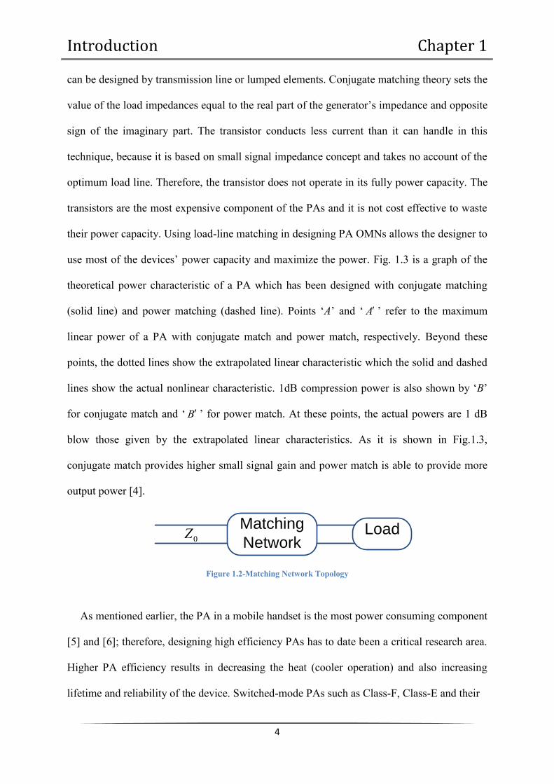
Introduction Chapter 1
4
can be designed by transmission line or lumped elements. Conjugate matching theory sets the
value of the load impedances equal to the real part of the generator’s impedance and opposite
sign of the imaginary part. The transistor conducts less current than it can handle in this
technique, because it is based on small signal impedance concept and takes no account of the
optimum load line. Therefore, the transistor does not operate in its fully power capacity. The
transistors are the most expensive component of the PAs and it is not cost effective to waste
their power capacity. Using load-line matching in designing PA OMNs allows the designer to
use most of the devices’ power capacity and maximize the power. Fig. 1.3 is a graph of the
theoretical power characteristic of a PA which has been designed with conjugate matching
(solid line) and power matching (dashed line). Points ‘A’ and ‘ A ’ refer to the maximum
linear power of a PA with conjugate match and power match, respectively. Beyond these
points, the dotted lines show the extrapolated linear characteristic which the solid and dashed
lines show the actual nonlinear characteristic. 1dB compression power is also shown by ‘B’
for conjugate match and ‘ B ’ for power match. At these points, the actual powers are 1 dB
blow those given by the extrapolated linear characteristics. As it is shown in Fig.1.3,
conjugate match provides higher small signal gain and power match is able to provide more
output power [4].
LoadMatching
Network0Z
Figure 1.2-Matching Network Topology
As mentioned earlier, the PA in a mobile handset is the most power consuming component
[5] and [6]; therefore, designing high efficiency PAs has to date been a critical research area.
Higher PA efficiency results in decreasing the heat (cooler operation) and also increasing
lifetime and reliability of the device. Switched-mode PAs such as Class-F, Class-E and their

Introduction Chapter 1
5
div
dBP O
UT
/1
divdBPIN /1
Conjugate match
Power match
Figure 1.3-Compression characteristics for conjugate and power match [4]
many variants, theoretically can provide high efficiency performances. Achieving high
efficiency in multiband applications is even more complex and difficult. Providing the same
performance and high efficiency in all working bands is a challenging task, because their
performances are frequency dependent due to requiring optimum output termination and
harmonic elimination in all bands at the same time. Due to this difficulty and high demand of
multiband high efficiency PAs, the research covered in this thesis explores the design of PAs
to operate with high efficiency in all frequency bands of multiband applications.
1.3 Outline of Work and Structure of Thesis
This research is mainly concentrated on developing a methodology to design highly
efficient multiband PA which can meet the requirement of cognitive radio systems. As
mentioned earlier, switched-mode PAs are good candidates to provide high efficiency
performances and in this work, Class-E PA is chosen due to its design simplicity, requirement
of slower devices compared to other switched-mode PAs and less sensitivity to parameter
variations [7]-[8]. The objectives of this work are:

Introduction Chapter 1
6
Proposing a new methodology of designing a switched-band MN to reduce the loss
and nonlinearity of switches along with an analytical solution for them, to prove
the validity and observe the coverage region of the MNs and shorten the design
time.
A methodology of designing high efficiency single-band Class-E PA with
distributed MN has been discovered.
A dual-band Class-E PA based on the proposed single-band PAs has been designed
and delivers high efficiency performances.
One of the proposed switched-band MN has been used to design a switched-band
Class-E PA.
The effect of shunt capacitance across the transistor in a Class-E PA topology on
engineering the waveform and accordingly on the efficiency, has been studied.
The research and objective of this work is explained in the next six chapters. The content
of each chapter is discussed briefly here. An overview of all the chapters is shown in Fig. 1.4.
Chapter 1Introduction
Chapter 2Background
Chapter 3Literature review
Chapter 4 MNs
Chapter5Dual-Band
PAsChapter 6Switched-Band
PAs
Chapter 7Conclusion
Figure 1.4-Overview of the thesis chapters

Introduction Chapter 1
7
Chapter 2 presents all of the basic criteria to design a PA, such as: some important
specifications (output power, gain, efficiency and linearity), classes of PAs and linearization
techniques. Also, different available switches are presented in this chapter to find the
appropriate switch for the application of this work.
Chapter 3 is a literature review on frequency adaptive PAs. This chapter starts with
studying all the possible approaches to design frequency adaptive PA: multiband and
switched-band PAs. All the reported multiband and switched-band PAs, to the author’s
knowledge, are included and discussed in this chapter. The performance and circuit diagram
of all the reported multiband and switched-band PAs are summarized in two tables.
Design, techniques and equations for the proposed switched-band MNs are discussed in
Chapter 4. Three techniques to design switched-band MNs are presented in this work. These
MNs provide the required impedances for two different frequencies by means of a detachable
stub and switching between open and short circuit stubs. Through this technique, the MNs are
capable of providing a match for more than two frequency bands. Analytical solution for all
the MNs have been derived to investigate range of frequencies and impedances achievable,
give more precise results and shorten the design stage. These MNs can be applied for many
applications (e.g. PAs, LNAs, Antennas etc). The MNs are compared in terms of their
accuracy and size. To apply the selected MN to design a PA, a dual-band harmonic tuned MN
is presented. The network is composed of a fundamental matching circuit and a second
harmonic termination circuit. The example demonstrates accurate matching capability at the
fundamental and open circuit at the second harmonic frequencies. The MNs are designed,
fabricated and tested.
The proposed technique of designing a high efficiency single-band and dual-band Class-E
PA is described in Chapter 5. Initially, the technique is applied to design single-band PAs to
prove the validity of technique and also have it as a reference design to compare the

Introduction Chapter 1
8
performance of the technique in dual-band application. After that, design of two dual-band
Class-E PAs is presented with two different transistors; Gallium Arsenide Heterojunction
Field Effective Transistor (GaAs HFET) and Gallium Nitride High Electron Mobility
Transistor (GaN HEMT). These PAs are designed without switches to minimize the number
of components and reduce the losses introduced by switches. High efficiency is observed
from these PAs but higher efficiency is obtained in one band and relatively lower in the other
band. The effect of the shunt capacitor across the transistor on efficiency is studied and the
reason for the difference in efficiency of both bands has been investigated.
To overcome the efficiency difference of the dual-band Class-E PA (in Chapter 5) and to
maintain the same performance in terms of output power and efficiency at both bands of
operation, a switched-band Class-E PA has been proposed in Chapter 6. Switches have been
applied in the OMN of the switched-band PA to switch between two optimum termination
impedances and switching shunt capacitor value across the transistor at two different
frequencies. This PA is called Switchable Matching PA (SMPA). Later, another switched-
band Class-E PA has been designed with dual-band OMN and switched shunt capacitor and
called Fixed Matching PA (FMPA). The FMPA reduces the number of switches in the OMN
compared to the SMPA. This chapter is finished by a discussion on performance of dual-band
and switched-band PAs.
The last chapter, Chapter 7, is a summary and conclusion of this research. Achievements
of this study are also discussed and this thesis is finished by proposing future works.
9
Chapter 2
Power Amplifier Theory This chapter will present all of the basic criteria to design a power amplifier. The Power
Amplifier (PA) converts DC input power to deliver RF output power at a great magnitude (as
high as required to pass through wireless medium). Descriptions of some important
definitions such as: Output power, Efficiency, Gain and Linearity, are discussed in the first
section. Then, different classes of operation for PAs are explained briefly. Devices and
linearization techniques that they are essential to design Radio Frequency Power Amplifier
(RFPA) are also covered.
2.1 Specification of Power Amplifier
Some important figures of merit are used to describe the performance of a PA
quantitatively. These values are useful when comparing how well different techniques of PA
will perform.
2.1.1 Output Power and Gain
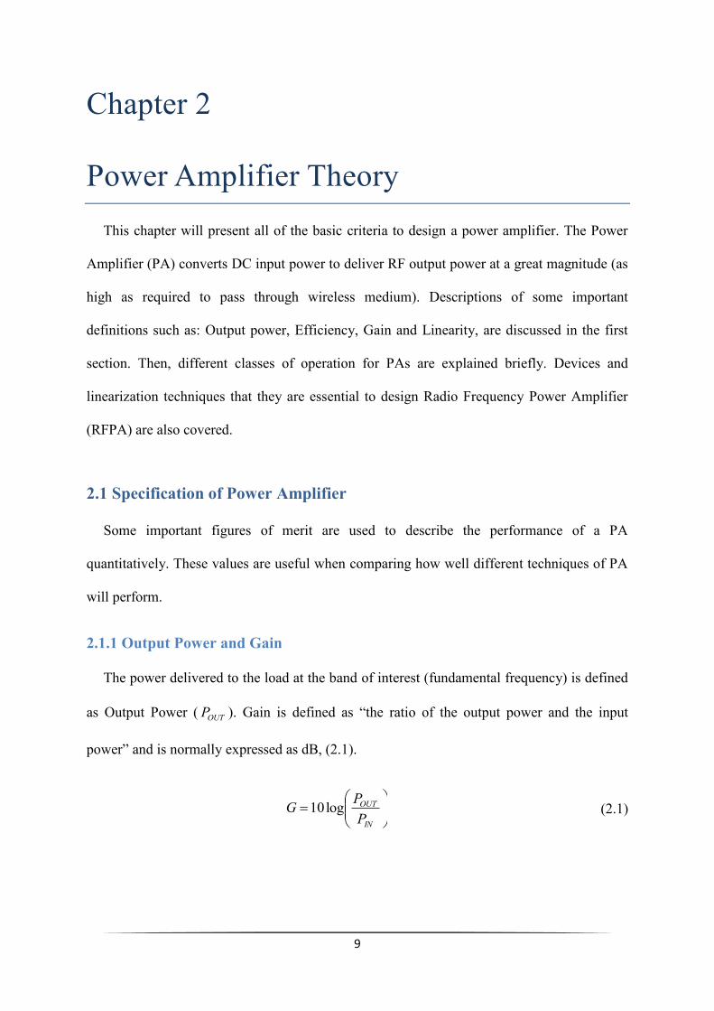
The power delivered to the load at the band of interest (fundamental frequency) is defined
as Output Power ( OUTP ). Gain is defined as “the ratio of the output power and the input
power” and is normally expressed as dB, (2.1).
IN
OUT
PPG log10 (2.1)

Power Amplifier Theory Chapter 2
10
2.1.2 Efficiency
The next and probably the most important one is efficiency and this can be divided into
two groups: Drain efficiency (η) and Power Added Efficiency (PAE). The DC power ( DCP )
and RF input power ( INP ) are the inputs of a PA, Fig. 2.1. Some of the inputs will appear in
the harmonic frequencies and some will dissipate inside the PA.
PAinPoutP
DCP
Figure 2.1-Power in PA
Drain efficiency is used to calculate how efficiently the DC power has been converted to
the RF output power:
DC
OUT
PP
(2.2)
PAE is very useful to show the PA’s performance, as it includes the gain of the PA as
well. The PAE is defined as:
DC
INOUT
PPPPAE
(2.3)
High efficiency PAs are preferred to increase battery life, reduce the power dissipation,
lower the cost and minimize the size [9]. All the possible losses of a PA are recognized as
shown in Table 2.1 with the possible solutions to minimize these losses and accordingly
maximize the efficiency of the PA [10]:
Power Amplifier Theory Chapter 2
11
Table 2.1-Possible losses in PA with the possible solutions
Losses Solutions
Dissipation power in the transistor Avoid overlapping between voltage and
current (switched mode PA)
Some of the output power appears at
harmonic frequencies Terminate the harmonics reactively
Losses in the components Utilize distributed MNs
2.1.3 Linearity
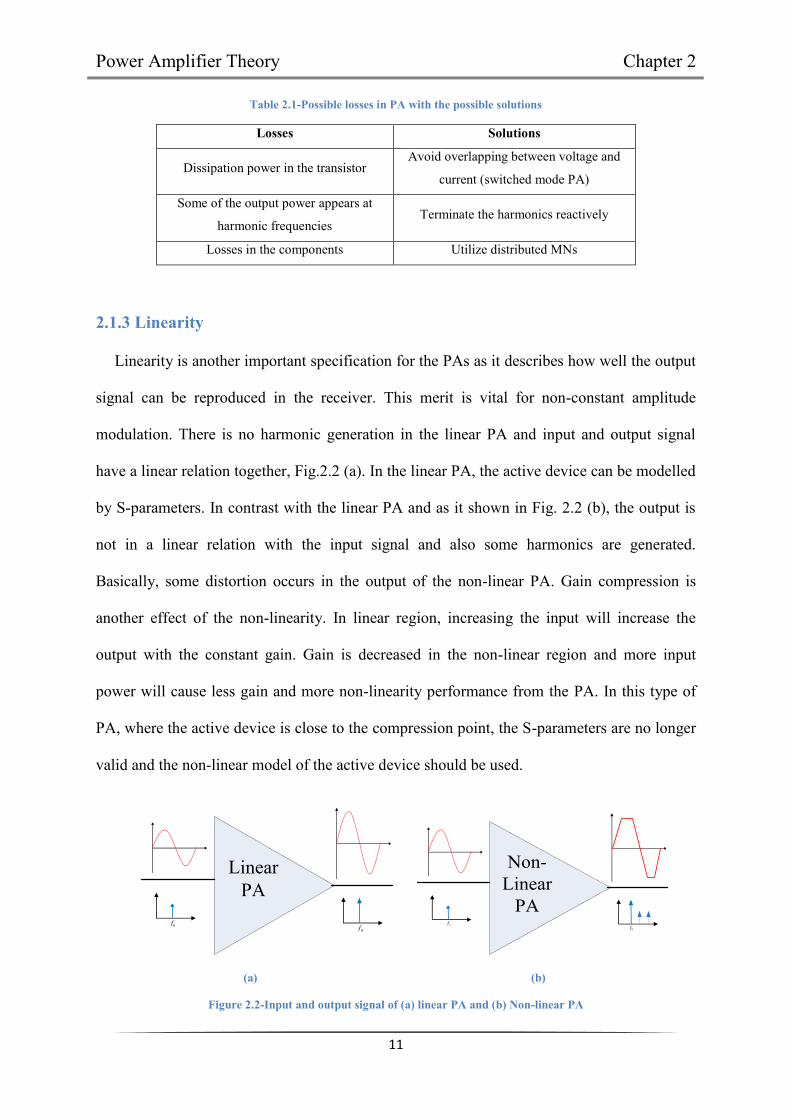
Linearity is another important specification for the PAs as it describes how well the output
signal can be reproduced in the receiver. This merit is vital for non-constant amplitude
modulation. There is no harmonic generation in the linear PA and input and output signal
have a linear relation together, Fig.2.2 (a). In the linear PA, the active device can be modelled
by S-parameters. In contrast with the linear PA and as it shown in Fig. 2.2 (b), the output is
not in a linear relation with the input signal and also some harmonics are generated.
Basically, some distortion occurs in the output of the non-linear PA. Gain compression is
another effect of the non-linearity. In linear region, increasing the input will increase the
output with the constant gain. Gain is decreased in the non-linear region and more input
power will cause less gain and more non-linearity performance from the PA. In this type of
PA, where the active device is close to the compression point, the S-parameters are no longer
valid and the non-linear model of the active device should be used.
LinearPA
0f
0f
Non-Linear
PA
0f
0f
(a) (b)
Figure 2.2-Input and output signal of (a) linear PA and (b) Non-linear PA

Power Amplifier Theory Chapter 2
12
Different techniques are available to measure the linearity of the PA [11]:
C/I (Carrier to Inter-modulation): is a traditional technique. Two or more carriers with
the same amplitudes are used to drive the PA. By comparing the third order and
intermodulation distortion (IMD) product to the carriers, the C/I can be found which
is desired to be about 30dB [11].
NPR (Noise Power Ratio): In this technique, a PA is driven with Gaussian noise
with a notch in its spectrum. The notch power (which appears because of the non-
linearity of PA) over the total power is NPR. It is mostly used for broadband Pas
[11].
ACPR (Adjacent Channel Power Ratio): this measures the effect of non-linearity
into an adjacent channel. The ratio of the out-of-band power (the power leaked to
the adjacent channel) to the in-band power is ACPR.
ch
adj
dPSD
dPSD
ACPR dBc
)(
)(
log10 (2.4)
Where, )(PSD is the power spectral density of the signal in bandwidth of
adjacent channel )( adj and bandwidth of the main channel )( ch , [11] and [12].
EVM (Error Vector Magnitude): is showing the effect of non-linearity on the
detection process and focusing on distortion in the main channel. The deviation of
the actual signal vector from the desired signal vector calculates with EVM, Fig.
2.3. EVM can be calculated in the limited number of symbols )(K :
Kkk
Kkkk
RMSR
RSEVM 2
2
(2.5)
Where, kS and kR are the actual vector and the desired vector, respectively [11] and [12].

Power Amplifier Theory Chapter 2
13
I
QA
ctua
l Vec
tor
Desired
Vect
or
Error Vector
Figure 2.3-Error Vector
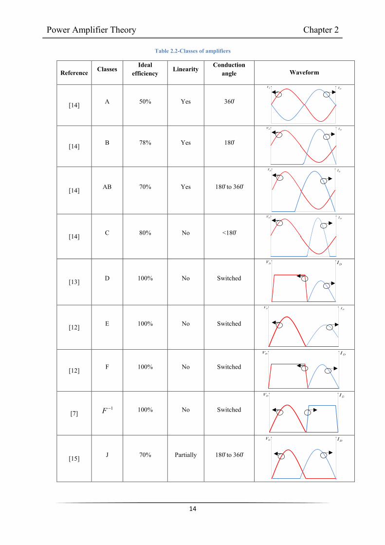
2.2 Classes of Power Amplifiers
There are different classes of PA and they are classified based on their bias point and
Matching Network (MN) topology [11]. Different classes of amplifiers and their specification
are summarized in Table 2.2 and each of the classes is explained briefly in this section.
Classes of PAs can be categorized in two groups: the transistor is the voltage controlled
current source (linear) or acts as a switch (nonlinear). In switch-mode PA, the transistor is
considered as two ideal conditions such as, ON state (short circuit) and OFF state (open
circuit). Improving efficiency will cause some nonlinearity in the PA and we can say there is
a trade of between linearity and efficiency. Depending on specific requirements a highly
efficient or a highly linear PA is used. Linear PAs are used in base stations and efficiency of
PA is a crucial factor in hand held units [13].
Class A: is the classic PA and the transistor is biased in linear region and always ON with
continuous current conduction. This class offers high linearity and gain in broadband
application at the cost of low power and efficiency. The output voltage and current waveform
has the same shape (for example sinusoidal) as the input signals (sinusoidal) without
harmonic content, [13] and [14]. The output power and efficiency for Class-A are:
Power Amplifier Theory Chapter 2
14
Table 2.2-Classes of amplifiers
Reference Classes Ideal
efficiency Linearity
Conduction angle Waveform
[14] A 50% Yes 360
DVDI
[14] B 78% Yes 180
DVDI
[14] AB 70% Yes 180 to 360
DVDI
[14] C 80% No <180
DVDI
[13] D 100% No Switched
DVDI
[12] E 100% No Switched
DVDI
[12] F 100% No Switched
DVDI
[7] 1F 100% No Switched
DVDI
[15] J 70% Partially 180 to 360
DVDI

Power Amplifier Theory Chapter 2
15
4
2max2 L
LDDoutRIRIP
(2.6)
DD
KneeDD
DDDD
L
in
out
VVV
VIRI
PP
24
2max
(2.7)
As DDI is 2maxI ; in the perfect scenario, KneeV is zero and the efficiency is 50
21
%. The
low efficiency of Class-A encouraged PA designers to reduce conduction angle below 360,
such as Class-AB, B and C. Conduction angle means the angle that the active device is ON
and conducting current [14].
Class-B: is similar to Class-A with slightly difference in biasing (biased close to cut-off).
The conduction angle of this class is 180 as the active device is ON for half of the cycle
(positive side of the input signal). The amplitude of the output signal is proportional to the
input signal and the drain current shape is unchanged, this class is classified as the linear PA
[14]. By reducing the conduction angle from 360 to 180, the overlap between current and
voltage waveforms is decreased and efficiency is increased compared to Class-A [11]. This
class is mostly applied in push-pull PA [11]. The DC current can be found by Fourier
coefficient (2.8), and the efficiency (2.9):
20
2sin21 T
L
DD
L
DDD R
VdttRV
Ti
(2.8)
%5.7844 2
2
DDL
DDL
in
out
VRVR
PP
(2.9)
Class C: is biased at or below the cut-off and its conduction angle is less than 180. This
class presents sinusoidal voltage waveform and narrow current pulses [10]. By reducing the
conduction angle towards zero, the efficiency is increasing towards 100% at the cost of
decreasing output power to zero. The best compromise is reported in [11], which provide
efficiency of 85% with 150 of conduction angle.

Power Amplifier Theory Chapter 2
16
Class D: The transistor acts as a switch and has two extreme values; zero and DDV . Two
transistors are applied in a Class-D PA to provide a square waveform for the drain voltage.
This class is a non-linear PA as the output and input have no linear relation. The Output
Matching Network (OMN) in this class provides open circuit for harmonics. Theoretically,
efficiency of 100% is expected from Class-D PA. Practically, this class has lower efficiency
due to losses. Switching speed and drain capacitance are the main sources of losses. Due to
the finite switching speed, the transistor conducts current while it is in its active region and
causes losses in this class of PA. Also, the other main source of losses is charging and
discharging the drain capacitance which dissipates power proportional to 2
2DDV . This
drawback has been covered in Class-E PA [11] and [13].
Class F: Class-F and Class-E are the most popular switched-mode PAs. Square voltage
waveform and half sinusoidal current waveform are expected from a Class-F PA. The odd
harmonic resonator in the OMN shapes the drain voltage to be a square waveform, as the
drain voltage is sum of fundamental and odd harmonic voltages. The half sinusoidal current
is achieved by biasing the active device at pinch off [12]. The output filter in Class-F
configuration is more complex than other PA circuits [11]. Open circuit termination in odd
harmonic and short circuit termination in even harmonic frequencies are required [14].
Class 𝐅−𝟏: is basically similar to Class-F PA with different harmonic termination criteria.
Odd and even harmonic frequencies are required to be terminated with short and open circuit
impedances. The obtained waveform of this class as shown in Table 2.2 is required to have
half-wave rectified voltage and square current [7].

Power Amplifier Theory Chapter 2
17
Class J: is capable of providing linear performance with high efficiency like Class-B. The
starting point to design a Class-J PA is Class-B. Half sinusoidal current and voltage
waveforms are observed in this class. Presenting the second harmonic component in voltage
provides half-wave rectified sinusoidal voltage. The impedance requirements at the output
port of the transistors are, [4] and [15]:
LLf jRRZ 0
(2.10)
Lf RjZ8
3002
(2.11)
003 fZ (2.12)
Impedance at the fundamental frequency, second and third harmonic frequencies represent
by 0f
Z , 02 fZ and
03 fZ ; also, the load substitute with LR .
The focus of this thesis is on Class-E PA. Class-E is explained more in detail in the next
section.
2.2.1 Class-E PA
It is a switched amplifier and the active device works as a switch. It was invented in 1970s
by Nathan and Alan Sokal (father and son) [19]. The basic topology of the Class-E PA is
shown in Fig. 2.4.
Figure 2.4-Class E Amplifier [20]

Power Amplifier Theory Chapter 2
18
2L and 2C are the resonators and R is a load. Supply choke ( 1L ) has high inductance to
provide open circuit for RF signals [21]. The shunt capacitor is shown by 1C in Fig. 2.4 which
contains the internal capacitance of the transistor and the external capacitor. In the OFF state
of the transistor, current flows through the shunt capacitor and in the ON duration current
flows through the transistor; where the transistor is in saturation mode [20]. This topology
aims to avoid conducting current and existing voltage at the same time and reduces overlap
between them. Therefore, the power dissipation in ideal switches is zero as it is multiplication
of voltage and current and provides a high efficiency nearly to 100% [18] and [22]. In
practice, limiting factors of the efficiency are drain to source saturation resistance and loss of
parasitic element [23]. Most of the dissipated power is in the transistor because while
transistor is ON, it has some low impedance and the voltage is not completely zero. In this
duration, internal capacitances store energy and produce some current while transistor is OFF
[20] and [22]. Moreover, in practice, even with the proper switch device, the switching time
may be a fraction of the ac cycle and lose some power. In designing a Class-E amplifier we
should be concerned about minimizing the switching time and it could be done by designing
a proper non-resistive load network [20].
As explained earlier, Class-E PA is a transition between pinch-off and saturation region
and ideal Class-E load line (red line) is shown in Fig. 2.5. The OFF state of the transistor is
represented with the horizontal line (current is zero) and the ON state is the vertical line
(voltage is zero) [18].
The OMN plays a crucial role in designing a highly efficient Class-E PA. The OMN
includes a set of specific valued components at the design frequency to avoid any overlap
between voltage and current waveforms; which in ideal case results in 100% efficiency. In
practice some of the delivered power will appear in second and third harmonic frequencies.

Power Amplifier Theory Chapter 2
19
Figure 2.5- Transistor I-V characteristic and Class-E load line
To maximize the efficiency, all harmonics should be open circuit. The transistor should be
biased at pinch off and driven into compression, so the transistor will be ON for the forward
cycle of sinusoidal input RF waveform and for all of the reverse cycle the transistor is
switched OFF.
2.2.1.1 Class-E Design Equations
The first stage of designing a Class-E PA is to calculate optimum parameters of OMN.
Equations (2.15) to (2.18), taken from [16], are applied to provide values of components (i.e.
load resistance ( R ), shunt capacitance ( 1C ), series capacitance and inductance, ( 2C ) and ( 2L
) respectively). These equations are derived from a time domain equation, according to the
required voltage and current assumption across the transistor, in ON and OFF state,
respectively, (2.13) and (2.14).
0|)( TtD tV (2.13)
0|)(Tt
D
dttdV
(2.14)
DV is the voltage across the transistor and T is the period of the input signal. These
components are calculated based on specific supply voltage DV and required output power
outP . Loaded quality factor ( LQ ) is a free choice variable and chosen by designers based on a
trade-off between operating bandwidth and rejection of harmonics. With the duty ratio set at
dI
minI
kneeV maxV )(VVDS
maxI

Power Amplifier Theory Chapter 2
20
the usual choice, 50%, the minimum value of LQ is 1.7879. The most desirable range to
provide acceptable efficiency and linearity is between 5 and 10.
2
2 402444.0451759.015768.0L
QQPVR
Lout
D (2.15)
DLL LQQRC 221
6.003175.191424.0144668.5
1
(2.16)
DLL LQQRC 22
2.07879.1
101468.11104823.011
(2.17)
RQL L2 (2.18)
2.3 Active Devices
In some applications, switches are required in the circuit. Different types of switches are
discussed here. Switching devices are used in circuits for opening and closing a connection or
for changing the branches. Ideally, a switch should present zero resistance in the ON state
and infinite resistance in the OFF state; whereas a certain amount of resistance on connection
state and a finite resistance on disconnection state will be presented by a switch in practical
cases. Isolation and insertion loss are the fundamental parameters to describe a switch’s
performance. Measurement of the power not transferred to the load when the switch is OFF is
named isolation (2.19), and insertion loss is a transmission loss through the switch in ON
state (IL) [24]. Low insertion loss and high isolation switches are desired.
OFFOUTONOUT PPIsolation (2.19)

Power Amplifier Theory Chapter 2
21
The brief descriptions of some switching devices are provided in the next sections. Some
factors are important to select a suitable switch such as switching speed, power handling
capacity, and cost. These factors are discussed later on and accompanied with a graph to
compare performance of switches in the published multiband PAs.
2.3.1 MEMS
Micro Electro Mechanical Switches (MEMS) provide open or short circuit by mechanical
movement. The mechanical movement is forced by electrostatic, magnetostatic, piezoelectric
or thermal design. There is almost no power loss in MEMS switches because they hardly
consume any current. MEMS switches are very linear devices. These switches are fabricated
with air gap and provide high isolation and low insertion loss of about -0.1 dB. On the other
hand, MEMS switches have some drawbacks such as low switch speed, limited power
handling (20-50mW) and requiring high voltage to drive. These switches are not reliable and
their efficient life time is 0.1-10 billion cycles only [25] and [26].
2.3.2 Varactors
Varactor diodes are P-N junction voltage controlled devices [24]. By changing the bias
voltage which is applied to the varactor diode the value of capacitance and resistance will
vary [27]. The varactor diodes work in reverse bias, so no current is required (i.e. no power
loss) [28]. Varactor diodes can be modelled with lumped elements as shown in Fig. 2.6. This
model consists of variable junction capacitance ( )(VCJ ) and variable series resistance (
)(VRS ), and PC is fixed parasitic capacitance. The package parasitic effect has been model
by aid of PL [27].

Power Amplifier Theory Chapter 2
22
PL
PC VCJ
VRS
Figure 2.6-Varactor diode equivalent circuit
2.3.3 PIN Diode
A PIN diode is a semiconductor current controlled device [24]. The high resistivity
intrinsic I-region which is sandwiched between P- and N-type regions is a general structure of
a PIN diode [24] and [29]. Holes and electrons are injected into the I-region in forward bias
of PIN diode and the PIN diode appears as a resistor. In the reverse bias, the I-region has no
stored energy and PIN diode acts as a parallel plate. The equivalent circuit model of PIN
diode in OFF and ON state is illustrated in Fig. 2.7.
PL
SR
PL
TC PR
(a) (b)
Figure 2.7-lumped element model of PIN diode (a) forward bias and (b) reverse bias
The equivalent circuit of a PIN diode in forward bias (Fig. 2.7 (a)) consists of a series
resistor ( SR ) and a small inductor ( PL ). This inductor represents the package properties of
the PIN diode. The resistance of a PIN diode in forward bias can be found by, [24] and [30]:

Power Amplifier Theory Chapter 2
23
FPNS I
WR
2
(2.20)
I-region width is W and forward bias current is FI . Electron and hole mobility are denoted
by N and P , respectively. The electrons and holes in I-region stay alive for an average time
that is referred to carrier life time ( ) [30]. The maximum and minimum forward resistance (
SR ) can be calculated by (2.20) at maximum forward current of 100mA and minimum
forward bias current of 10μA. Conduction higher current in a PIN diode will decrease the
resistance as it acts as a variable resistor. The equivalent circuit in reverse bias is composed
of the diode capacitance ( TC ), loss element ( PR ) and parasitic inductance ( PL ), Fig. 2.7
(b).The value of the capacitance is:
WACT
(2.21)
Where, is dielectric constant and A is area of junction [29]. A PIN diode can be
connected in series or shunt in the circuits. Series connection provides low insertion loss
whereas when high isolation is required a shunt connection is applied that is capable of
handling more power, and it is easier to cool the device [14] and [30]. The junction
temperature of a PIN diode increases while it is controlling the power signal and therefore,
dissipates some power [24]. The maximum allowable power dissipation is:
DCDCSRFd VIRIP 2 (2.22)
Similar to all diodes, PIN diodes have two terminals; therefore separate DC biasing is
required from RF path with an external decoupling element. As mentioned above, a PIN
diode is a current control device and therefore consumes high amounts of power. Small
physical size, high switching speed, low package parasitic reactance, ability to control large
RF-signal-power, low cost and low loss are the advantages of PIN diodes [24] and [31].

Power Amplifier Theory Chapter 2
24
Because of wide I-region of PIN diode, it can handle large RF voltages which other diodes
are unable to handle.
2.3.4 FET Switches
Field Effect Transistor (FET) switches are a good candidate due to relatively high ratio
between their ON and OFF state resistance. To control switching in FET devices, the voltage
on their gate needs to be adjusted. Basic switch performances of PIN diode and FET switches
are fairly similar as both have ON state resistance and OFF state capacitance. The difference
is in the amount of DC power consumption. FET switches require very simple bias network
(high resistor). PIN diodes require a bias current in the ON state and consequently have more
complicated bias networks. FET switches can provide broadband operation. By increasing the
frequency, the isolation of the FET is degraded due to the drain-to-gate capacitance and also
has high loss [14] and [31].
2.3.5 Performance Comparison
The published switched-band PAs (which they are discussed in Chapter 3) utilise different
switches such as: MEMS, PIN, FET and varactor diode. One way to analyse the
performances of these switches in the switched-band PAs application, is to use the published
data of the performance of these switches. PAE and output power of the switched-band PAs
that use a switch, have been considered and plotted in a graph as shown in Fig. 2.8. As
illustrated in the graph, highest PAE with desired output power is provided by PIN diode.

Power Amplifier Theory Chapter 2
25
Figure 2.8-Comparison between PAE and output power of switches used in multiband matching network techniques
2.4 Linearization Techniques
Any signals which are non-constant envelope require linear amplification. As mentioned
earlier, there is trade-off between efficiency and linearity; by achieving one we can lose the
other. Switched-mode PAs are capable to provide high efficiency but nonlinear performance.
By considering power series for PAs as:
....32 inininout cVbVaVV (2.23)
With higher input power, output voltage has a more nonlinear relation with the input
power. The switched mode PA requires high input power. The nonlinearity causes some
problem such as, splatter into next channels and errors in detection and reproduction. By
applying one of the linearization techniques and providing linear output signal, both
requirements (high efficiency and linearity) can be fulfilled. Linearization techniques are not
applied just to improve linearity; they are also used to develop efficiency by decreasing the
need of back off [11]. Basically, in linearization techniques, amplitude and phase of the input
are used as a template and will be compared to those of the output, allowing the required
correction to be determined and applied [13].
36
38
40
42
44
46
48
50
20 25 30 35
PA
E (%
)
Output Power (dBm)
MEMS
PIN
FET
Varactor

Power Amplifier Theory Chapter 2
26
Closed and open loop are two linearization methods. Open loop is not as accurate as
closed loop technique, but it can handle much wider bandwidth [13]. There are three
linearization techniques; feedback, feed-forward and pre-distortion. Feedback is a closed loop
linearization technique, whereas feed-forward and pre-distortion are open loop. Fig. 2.9
summarizes the linearization techniques from [11], [13]-[14], [32] and [33] with their
specifications and more explanation of these techniques is in the following section.
Linearization
Techniques
Feedback Feed-Forward Pre-distortion
RF FeedbackEnvelop
FeedbackPolar-Loop
Feedback
Cartesian
Feedback
Delay Overcome delay
No correction AM-
PM distortion
Appropriate for
Class-A or -AB
Correct AM-
PM distortion
Poor overall
performance
Operate in wide
bandwidth
Very wide bandwidth
Difficult to implement
Poor overall
efficiency (due to the
additional PA)
Broadband
operation
Multichannel
application
Figure 2.9-Linearization Techniques
2.4.1 Feedback
There are four different techniques for feedback linearization: RF feedback, Envelope
feedback, Polar-Loop feedback and Cartesian feedback.

Power Amplifier Theory Chapter 2
27
RF Feedback
A small amount of RF output signal is entering back to the input of the PA and finds the
difference with its input. This technique suffers from delay (which cause instability) and loss
of gain at RF frequencies [11].
Envelope Feedback
By using the signal envelope as a feedback parameter, the problem of delay can be
resolve in the envelope feedback. The drawback of this linearization technique is its inability
to correct phase distortion (AM-PM distortion). Variation in phase of the output signal by the
change in amplitude of the input signal is known as AM-PM distortion [34].
Polar-Loop Feedback
Polar-Loop feedback overcomes the shortage in the envelope feedback technique by
adding a phase-locked loop. The amplitude and phase feedback path are separate and require
different bandwidths, therefore reduce the overall performance [11].
Cartesian Feedback
The Cartesian feedback applied modulation feedback in Cartesian component (I and Q).
Two identical feedback processes is applied to I and Q channels independently. In Cartesian
feedback, closed loop baseband feedback in I and Q channel is used to ensure that the vector
modulated output from the PA has I and Q components matching those at the input. The
drawback of this technique is narrow bandwidth performance [11] and [33].
2.4.2 Feed-Forward
As shown in Fig. 2.10 feed-forward consists of two amplifiers; main and error amplifier.
The input signal split into two branches; one goes directly to the main PA. The output of the
main PA is combined with the original delayed signal of other branch. The distortion

Power Amplifier Theory Chapter 2
28
component of the main PA is obtained and the error amplifier (which is a linear, low power
amplifier) amplifies this signal. The outputs of both amplifiers are combined and result in the
cancelling the distortion components from the main signal [11]. This technique is mainly
applied for high power PAs, such as cellular base station [14].
Main PA
Error PADelay
Delay
_
inRF outRF
Figure 2.10-Feedforward Linearization Technique
2.4.3 Pre-Distortion
This technique was common in analogue implementation [35] and then, thanks to Digital
Signal Processing (DSP) is popular in digital implementation as well [32]. In the pre-
distortion technique, the amplitude and phase of the signal are modified (using the inverse
characteristics of the PA) before the amplifier in such a way that by combining them a linear
output is generated. Concept of pre-distortion is shown in Fig. 2.11. When nonlinearity
characteristic of PAs change during their lifetime (with temperature or with changes in
environment) the fixed pre-distorter is unable to adopt its characteristic. Adaptive Pre-
distortion overcomes this drawback and is providing better performance and wider
bandwidth. The other type of pre-distortion is digital pre-distortion which can be used in
broadband and narrowband [11].

Power Amplifier Theory Chapter 2
29
Figure 2.5-Concept of Pre-distortion [36]
2.4.4 Envelope Elimination and Restoration
The basic idea of this technique is to provide a highly efficient linear RFPA by aid of
highly efficient and nonlinear RFPA and highly efficient envelope driver [11]. EER has two
paths as shown in Fig 2.12. One path just modulates the phase of the signal. The limiter
eliminates the amplitude modulation and provides the constant envelope signal for the PA.
This PA can operate in Class-C, D, E and F [11]. The other path provides the amplitude
modulation. The PA restores the envelope by varying the drain voltage to correct the output
amplitude. The amplitude and phase modulated signal add together and make the original
signal [37]. The phase information need to be delayed to enable both modulated signal arrive
at the same time. The switching speed is hundreds of MHz due to requirement of high
oversampling for switched-mode PAs and this is a challenge in wideband applications. The
other down side of EER is consumption of high power by the modulator which reduces the
efficiency [38].

Power Amplifier Theory Chapter 2
30
Limiter Delay PA
Envelope Detector
Driver
inRFoutRF
Figure 2.6-Envelope Elimination and Restoration
2.5 Discussion
This chapter presents all the required background knowledge for this research. At the
beginning, important metrics to evaluate performance of the PA such as, output power, gain,
efficiency and linearity, have been covered. Furthermore, different classes of PAs are
explained, starting with the linear Class-A and continuing to the switched-mode PAs. High
efficiency PAs (switched-mode PAs) are of interest to meet the requirement of modern
communication systems. To provide higher output power Class-F is preferred and Class-E is
more capable to achieve higher efficiency [10] and [17]. The advantage of Class-E PA is
having a small number of reactive components as well as high efficiency performance.
Another feature of the Class-E PA which makes it more preferable is that the internal
capacitance of the transistor can be absorbed as a component of OMN [18] and [39].
In the switched-band application, switches play an important role. A brief overview of
different switches presented. The switches introduce nonlinearity in the circuit. Also, the
switched-mode PAs (which are of interest in this research) are inherently nonlinear.
Linearization techniques are important for this research to provide linear output. Finally, the
linearization techniques which are vital for wireless communication to enhance the linearity
and efficiency of the PA were explained.

31
Chapter 3
Multiband and Switched-Band Power Amplifiers-A Literature Review
Increasing demand for wireless communication systems requires high efficiency,
multiband, adaptable and high linearity transmitters. A cognitive radio system is trying to
work in different frequency ranges in such way that it does not cause interference with other
communication systems, and does not get affected by interference from the other systems.
Designing adaptive front-end components has attracted lots of attention during the past
couple of years. The adaptive Power Amplifier (PA) is the most critical component to design.
As required for cognitive radio system the PA should be able to adapt its characteristics such
as frequency and power according to the environment. Designing highly efficient, adaptive
PAs is a critical research area.
One approach to design a PA to suit the requirement of the cognitive radio is the
broadband PA. A broadband PA covers the whole required bandwidth with the constant gain.
Fig. 3.1 shows the gain performance of an ideal broadband PA over the frequency. Class-A
can be a candidate to operate in the broadband applications. Higher efficient classes are
problematic to design broadband due to their requirement for harmonic terminations. Some
attempts to design broadband switch-mode PA has been done; one of them reported in [23] (a
broadband Class-E PA) to operate in multiband applications. Distributed second harmonic
termination has been designed with three half wavelength short circuit stubs in three different
frequencies in this PA.

Multiband and Switched-Band Power Amplifiers Chapter 3
32
One possible way to design broadband PAs is using wideband Input Matching Network
(IMN) and Output Matching Network (OMN) which is challenging and complex. Such PAs
are low in cost and small in size but at the cost of design complexity, less gain and lower
efficiency.
Gain
f
Figure 3.1-Frequency response of an ideal broadband PA
Balanced and distributed PAs are two examples of broadband PA. Balanced amplifier as
it is shown in Fig 3.2 consists of two identical amplifiers and two hybrid couplers. The input
signal divides into two parts with equal amplitude and 90 phase difference. Each of these
signals goes to one of the amplifiers. Outputs of amplifiers are recombined in the second
hybrid coupler. The hybrid coupler in input and output provide phase shift for any reflection
from amplifiers to compensate them at the terminating terminals; therefore, both amplifiers
are well matched in the balanced amplifiers. This amplifier is complex, as it requires two
couplers, two amplifiers and two DC supplies [40] and [41].
inV
Hybrid
Coupler
Hybrid
Coupler
outV
Amplifier
Amplifier
Figure 3.2-Balanced amplifier

Multiband and Switched-Band Power Amplifiers Chapter 3
33
A distributed amplifier contains several cascaded transistors, Fig 3.3. The gates of the
transistors are connected along a transmission line with the specific characteristic impedance
and length; and also the drains of the transistors are connected via another transmission line.
The main advantage of this amplifier is its operation in a very broad bandwidth. The circuit
of this amplifier is large and unable to perform with high gain and efficiency [40] and [42].
. . .
inV
outV
Figure 3.3-Distributed Amplifier
As mentioned in Chapter 1, design of highly efficient frequency adaptive PA is the main
aim of this thesis. Therefore, the broadband PA is not a good candidate. Other possible
approaches to a design frequency adaptive PA is: multiband PA (MB-PA) and switched-band
PA (SB-PA). This chapter explains these two techniques and presents an overview of the
researches have been done on designing MB-PA and SB-PA.
3.1 Adaptive Power Amplifiers
In this thesis, adaptive PA refers to the PAs that can adapt their frequency response to the
environment requirement. Techniques of designing an adaptive PA can be divided into two
main groups; known as: MB-PA and SB-PA. MB-PAs do not use switches in their circuit and
can provide concurrent amplification in different frequencies. A switch is a key component in
SB-PA and it works in one band at a time. These two kind of adaptive PAs are going to
explain in the following section along with some examples.

Multiband and Switched-Band Power Amplifiers Chapter 3
34
3.1.1 Multiband Power Amplifiers
The MB-PA is capable of working in different frequencies simultaneously. Gain over
frequency of an ideal MB-PA (dual-band in this example) is expected to be the same as it
shown in Fig 3.4. Table 3.1 summarises the techniques of reported MB-PA in chronological
order as well as their achieved results; below a short description of each method listed in the
Table 3.1 is provided.
Gain
f
Figure 3.4-Frequency response of an ideal dual-band PA
One technique of designing MB amplification is implementing multiple parallel amplifiers
for each operating band; such as a dual-band PA reported in [43] which was designed with
two parallel amplifiers. This PA is big in size and requires a large amount of components as it
required one PA for each frequency band. There is another technique with multiband input
matching network (MB-IMN) and multiband output multiband matching networks (MB-
OMN). This technique is smaller and has fewer components. The IMN and OMN are
designed without switches or tuneable elements and provide the required impedances and
optimise PA performance at individual working bands. MB-MN can be designed with
transmission line or lumped element. Distributed MB-MNs are more popular than lumped
element MB-MNs as the performance of the distributed element differs in different frequency
bands. First, MB-PAs with distributed MB-MN will be reviewed.
The dual-band PA in [44] has been designed with transmission lines and utilises quarter
wavelength stub at an adequate distance from the device for the proper impedance

Multiband and Switched-Band Power Amplifiers Chapter 3
35
termination. Low-pass Chebyshev-form impedance transformer is one way to design MB-
MN and it has been used in a reported MB-PA in [45]. Composite right/left-handed
transmission line (CRLH TLs) is another possible way of designing MB-MN which has been
used in [46], [47] and [48]. Harmonic terminations were neglected in [46], whereas, this
important factor is taken into account in [47]. The dual-band PA in [47] consists of two
CRLH diplexers in input and output with two amplifiers between them and as well as
matching at the fundamental frequency and terminating the harmonics.
A multi-section transformer has been used in the OMN in [49], [50] and [51]. Each section
of the transformer has been designed to match at a specific frequency; tank circuit [51] or
branched stub [49] is used in each section to prevent any mismatch at other frequencies. A
three section microstrip transmission lines used in the IMN and OMN of dual-band PA [52].
The first section was replaced with an open stub in the OMN with the purpose of terminating
harmonics. The result shown in the table for this PA is the simulation result. The OMN in
[53] has three sections:
Real-to-Complex impedance transformer: to transform complex impedances at the
two operating frequencies to real impedances
Transmission line: to tune the harmonics
Real-to Real Impedance transformer: to transform the obtained real impedances to the
system impedance. A distributed dual-band filter was designed for this purpose with
dual-band resonator and J-inverter.
T-type and Pi-type transformers are equivalent to quarter-wave transformer and have
different impedances for different frequencies. The author in [54] called them dual-
band/dual-impedance and they transform 50Ω to the real part of the required impedances at
two different frequencies. A dual-band/dual-susceptance stub is applied to provide the

Multiband and Switched-Band Power Amplifiers Chapter 3
36
imaginary part of the required impedance. However, this technique is not feasible for all the
frequencies and impedances as in some cases the width of the transmission line is not
practical.
Different operation modes in each working band are reported in [55] and [56]. The OMN
of [55] consists of two blocks; harmonic control and fundamental MN. The harmonic control
network designed with transmission line and length of them has been chosen in the way to
provide short circuit at 12 f and open circuit at 13 f (Class-F) and open circuit at 22 f and short
circuit at 23 f (Class- 1F ). A distributed OMN provides Class-AB condition at the lower band
and Class-J at the higher band in [56].
Distributed IMN and OMN have been designed based on load-pull/source-pull simulations
in [57]; the OMN consists of two sub-networks: harmonic termination and fundamental
matching. Two stubs provide short circuit at second harmonic of the fundamental frequencies
in its harmonic termination network. This PA has been used in [58] to design Doherty PA
later in June 2012. Doherty PA (DPA) contains two PAs: carrier PA and peaking PA which
they operate in Class-AB and Class-C mode, respectively. The main advantage of DPA is to
maintain high efficiency over wider range of input power [68]. Each component of a
conventional Doherty PA is replaced by a dual-band version in [59]. A dual-band branch-line
hybrid (using Pi-type transformers) replaces the input splitter. Dual-band carrier PA (Class-
AB) and peaking PA (Class-C) have been designed with dual-band MNs and followed by
dual-band phase offset lines.
There are some reported MB-PAs with lumped element MB-MNs; one of them is shown
in [60]. The lumped element MB-IMN and MB-OMN have been designed based on the load-
pull/source-pull simulation to operate in both working bands. A passive MN is applied in the
PA of [61] as well, to provide high reactive impedance and terminate the harmonics.
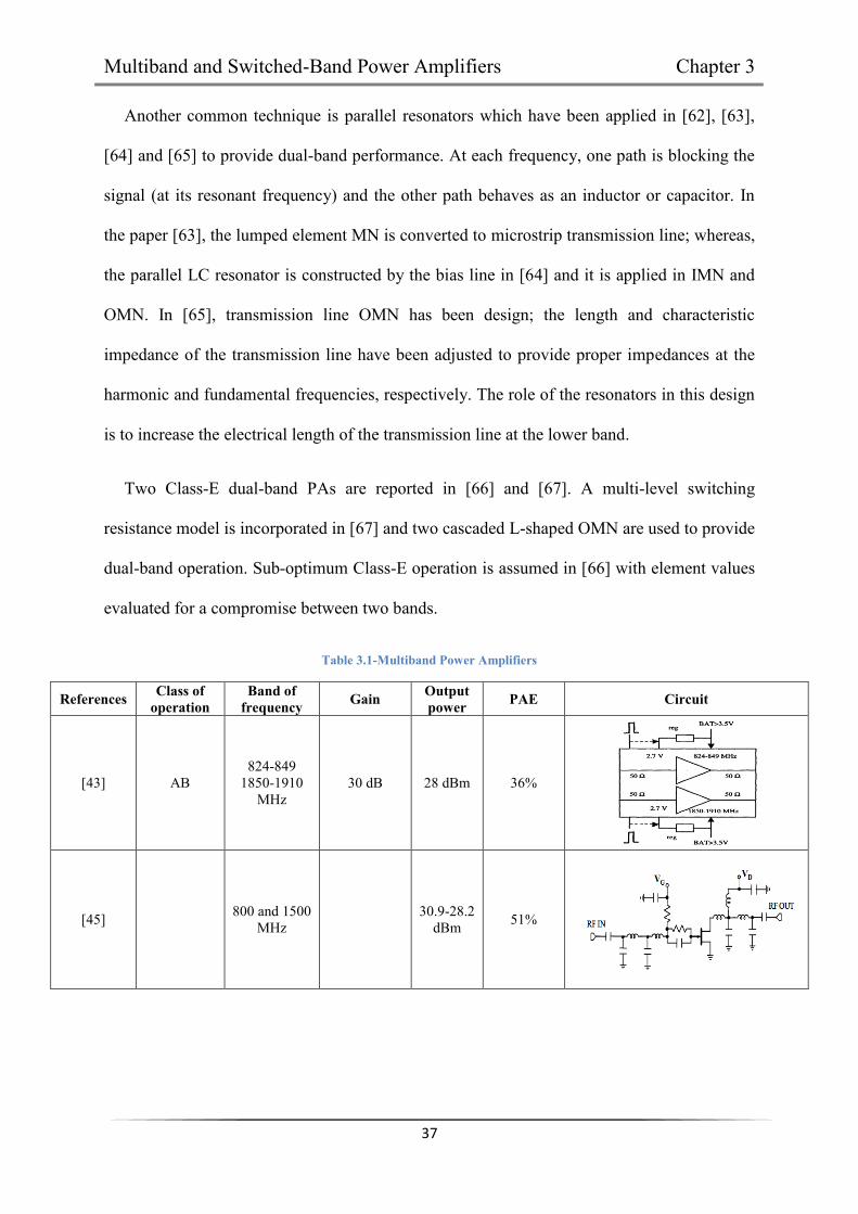
Multiband and Switched-Band Power Amplifiers Chapter 3
37
Another common technique is parallel resonators which have been applied in [62], [63],
[64] and [65] to provide dual-band performance. At each frequency, one path is blocking the
signal (at its resonant frequency) and the other path behaves as an inductor or capacitor. In
the paper [63], the lumped element MN is converted to microstrip transmission line; whereas,
the parallel LC resonator is constructed by the bias line in [64] and it is applied in IMN and
OMN. In [65], transmission line OMN has been design; the length and characteristic
impedance of the transmission line have been adjusted to provide proper impedances at the
harmonic and fundamental frequencies, respectively. The role of the resonators in this design
is to increase the electrical length of the transmission line at the lower band.
Two Class-E dual-band PAs are reported in [66] and [67]. A multi-level switching
resistance model is incorporated in [67] and two cascaded L-shaped OMN are used to provide
dual-band operation. Sub-optimum Class-E operation is assumed in [66] with element values
evaluated for a compromise between two bands.
Table 3.1-Multiband Power Amplifiers
References Class of operation
Band of frequency Gain Output
power PAE Circuit
[43] AB 824-849
1850-1910 MHz
30 dB 28 dBm 36%
[45] 800 and 1500 MHz 30.9-28.2
dBm 51%

Multiband and Switched-Band Power Amplifiers Chapter 3
38
[46] E 800 and 1700 MHz 22.2dBm 42.5%
[60]
AB
1.9 and 3.5 GHz 11-6 dB 24-17
dBm 20%
[61] AB 2.45 and 3.3 GHz 33-32.5
dBm
[65] F 1.7 and 2.14 GHz 5 dB 32.8-34.4
dBm 31.1-50%
[62] AB 2.4 and 3.5 GHz 18 dBm 42%
[63] AB 2.5 and 3.5 GHz 10.8-10.5 dB 68-54.5%
[47] CE 0.38 and 0.96 GHz 64.5-
61.2%

Multiband and Switched-Band Power Amplifiers Chapter 3
39
[49] AB 0.9, 1.8 and 2.1 GHz 12 dB 30 dBm 55-56-63%
[44] E 1.8 and 2.6 GHz 37.8-36.9
dBm 78.4-
61.3%
[64] B 1.7 and 2.14 GHz 9.8-10.5 dB 36.7-39.7
dBm 58.4-
59.9%
[55] F/ 1F 0.8 and 1.25
GHz 12 dB 40.6-41.8 dBm 81.7-80%
[50] AB 0.8 and 3.3 GHz 13-9 dB 30.1-30.5
dBm 62-53%
[51] AB 1.47,1.94 and 2.65 GHz
9.6-10-12.9 dB
30.5-31.5-30.5
dBm 60-54-57%
[56] AB/J 1.5 and 3.8 GHz 18-12 dB 37.3-35.7
dBm 47-52%
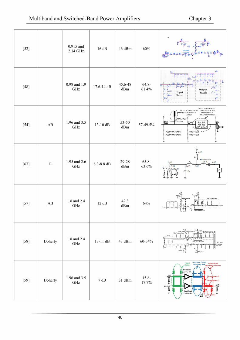
Multiband and Switched-Band Power Amplifiers Chapter 3
40
[52] 0.915 and 2.14 GHz 16 dB 46 dBm 60%
[48] 0.98 and 1.9 GHz 17.6-14 dB 45.6-48
dBm 64.8-
61.4%
[54] AB 1.96 and 3.5 GHz 13-10 dB 53-50
dBm 57-49.5%
[67] E 1.95 and 2.6 GHz 8.3-8.8 dB 29-28
dBm 65.8-
63.6%
[57] AB 1.8 and 2.4 GHz 12 dB 42.3
dBm 64%
[58] Doherty 1.8 and 2.4 GHz 13-11 dB 43 dBm 60-54%
[59] Doherty 1.96 and 3.5 GHz 7 dB 31 dBm 15.8-
17.7%

Multiband and Switched-Band Power Amplifiers Chapter 3
41
[66] E 1.2 and 3 GHz 13-8.5 dB 30-28
dBm 50-30%
[53] J 0.8 and 1.9 GHz 46 dBm 70%
3.1.2 Switched-Band Power Amplifiers
The SB-PAs utilize switches or tuneable elements to provide multi-band amplification.
The gain performance of an ideal SB-PA is desired to be the same as it shown in Fig 3.5 (in
this example, the PA works in two bands). Different SB-PA has been reported during last
decade and they are summarized in Table 3.2 according to their year of publications. Their
architectural technique is discussed briefly here.
Gain
f
Figure 3.5-Gain performance of an ideal SB-PA over frequency
The SB-PA can be designed in two ways:
Switching between numbers of narrowband PAs (Fig. 3.6 (a))
Switched-band matching networks (SB-MN) (Fig. 3.6 (b))

Multiband and Switched-Band Power Amplifiers Chapter 3
42
PA1
PA2
PAn
INPUT
OUTPUT
SB-IMNSB-OMN
INPUTOUTPUT
(a) (b)
Figure 3.6- SB-PA (a) switching between numbers of narrowband PAs (b) switched-band matching network (SB-MN)
The first technique utilizes a number of narrowband PAs and based on the environment
requirement one of them will be selected by using a switch. This technique is easy to
implement due to simplicity in the designing of narrowband PAs. Each of these narrowband
PAs are capable of providing high gain and good linearity, individually. As the number of
required operating bands increases this structure will become bulky and complex. A PA
based on this technique is expensive and noisy due to the existence of many internal
connections. Examples of this PA are reported in [69] and [70]. Two PAs (optimized for their
operating bands) and two bias circuits are designed with a bias switch in [69]. The bias
switch is selecting the band of operation by activating one PA and deactivating the other. In
[70], the first PA is common and then band switch is applied to choose the desired path for
each frequency. The performance of the lower band of operation (where the switch is ON) is
relatively smaller than the higher frequency (switch is OFF), as the loss of switch is high in
its ON state. Band selection is applied in [71] as well, by aid of conducting two different bias
currents. In this PA, a dual-band IMN and two individual OMNs for each band of operation
have been designed. Three-stage amplification has been used in [72] and there is band
selection control which switches between two bands of operation.
The second approach to have an SB-PA is to integrate the system with a SB-MN which
provides optimum matching at each operating frequency. This method, in comparison with

Multiband and Switched-Band Power Amplifiers Chapter 3
43
the other method, has a relatively low cost, smaller circuit and higher efficiency. SB-MNs
can be designed with distributed elements or lumped elements.
Distributed SB-MNs are designed by connecting or disconnecting the distributed element
into the circuit. In 2004, a technique for dual-band PA was introduced using an OMN to
provide the first frequency and a shunted switchable stub to produce the second frequency
[21]. ON/OFF state of switches provides optimum matching in two different frequencies. The
same technique was used in 2005 and 2010 with additional stubs to provide three bands of
operation in [73] and [74]. In 2006, the designers tried to make the transmission line shorter
and compact the circuits even more in [75] and [22]. This aim was achieved by implementing
a reconfigurable stub for the first MN. The reconfigurable stub consisted of two stubs with a
transmission line between them in [22]; and a series of transmission lines with switches in
[75]. Obviously, the number of switches increases in [75] and they introduce more losses in
the circuit. A 3-stage PA is illustrated in [90] in which the first two stages are driver stages
and provide required power for the input of the last stage. The last stage is the power stage
and uses a reconfigurable MN with the same technique introduced in [21] and [73]. A quad-
band PA is presented in [76]. The PA is designed specifically for the higher band of operation
and different MNs are connected via switches; by controlling the ON/OFF state of the
switches the performance of the PA is shifted to other required frequency bands.
Lumped element SB-MNs are designed in different ways. Here, they are classified in two
main groups: (i) utilizing variable performance of the switches and (ii) using switches to
control the value of an inductor or a capacitor. Variable performance of the switches is used
to provide optimum matching in different frequencies in technique (i). One example of these
SB-PAs is presented in [77], where a double stub MN is implemented in the input and output
networks. In this design, MEMS switches replace the shunt stubs to provide required

Multiband and Switched-Band Power Amplifiers Chapter 3
44
matching for both bands at the source and the load of the transistor. MEMS and varactors are
used in [78], where the ON/OFF state of MEMS and varying biasing of varactors provide
matching for different frequency bands. Anti-series varactor is another technique which is
shown by [28]. This technique used a high value resistor and two diodes that provide high
impedance for the centre of the tunable capacitors. Capacitance of varactors is controlled
based on the level of input voltage at C1 and C2 points marked in the schematic diagram.
Variable inductors are used in the RF choke and OMN of [79]. The PA in [80] uses BST
(Barium Strontium Titanate) varactors in the circuit to change impedance for different
frequencies. The BST varactors are tuned by two bias voltages and change the impedance of
the circuit.
The other technique (ii) uses switches to change the value of inductor or capacitor to
obtain a desired impedance based on the required operating frequencies. In [81],
reconfigurable capacitors and switches are implemented to produce required impedance at
two frequency bands. Changing the value of capacitors by controlling the ON/OFF state of
switches used in [82] varies the operating frequency in that model. Also, this technique has
multilevel output power with the aid of a switch to activate only two transistors at the same
time, to create a push-pull power amplifier. Parallel parasitic capacitance at the drain of the
transistor results in lower performance in the higher band. A PA with two switchable OMN
has been used in [83]. The first OMN utilizes switchable capacitor to change the load
impedance between two values to switch the value of output power. Another switchable
capacitor is used in the second OMN to switch between two bands of operation. A
broadband PA is followed by a reconfigurable OMN in [84] and [85]. The OMN uses two
parallel inductance-capacitance (LC) tanks in OMNs that adjust the inductance value using a
PIN diode; when the PIN diode is ON the parallel inductor is introduced into the circuit and

Multiband and Switched-Band Power Amplifiers Chapter 3
45
change the inductance value. ON and OFF states of the switch change the value of inductance
from large to small, thus changing the resonant frequency from 0.9 to 1.8 GHz.
In [86] and [87], SB-MN contains multiple paths which are connected via switches.
Connecting or disconnecting each path is executed by selecting the ON/OFF state of the
switches and the operating band of the SB-PA will alter accordingly. One of them is reported
in [86] which consists of two output paths and provide different operating frequencies based
on the chosen path. The PA in [87] is able to operate in two frequencies by aid of two output
paths which each of them provide two different bands. One path is operate at the time and
other path is deactivated by switching the shunt SPDT switches. ON state of the switches
provide short circuit at the intended frequency and will transform to open circuit at the drain
of the transistor.
Class-E SB-PAs are designed and reported in [81], [88] and [89]. A quad-band Class-E
PA is proposed in [88] which consist of four transistors and a single IMN and OMN. It works
in one of the frequency bands at a time and is switched between bands by controlling the gate
bias. A switched-band Class-E PA with finite DC-feed inductance is presented in [89]. A
switch is applied to achieve optimum performance in the selected band, while the inductors
are constant. The presented results for this PA in Table 3.2 are simulation results.
Table 3.2- Switched-band Power Amplifiers
References Switch Class of operation
Band of frequency Gain Output
power PAE Circuit
[72] B 0.9 and 1.8 GHz 28 dB 35 -32.5
dBm 48-44%
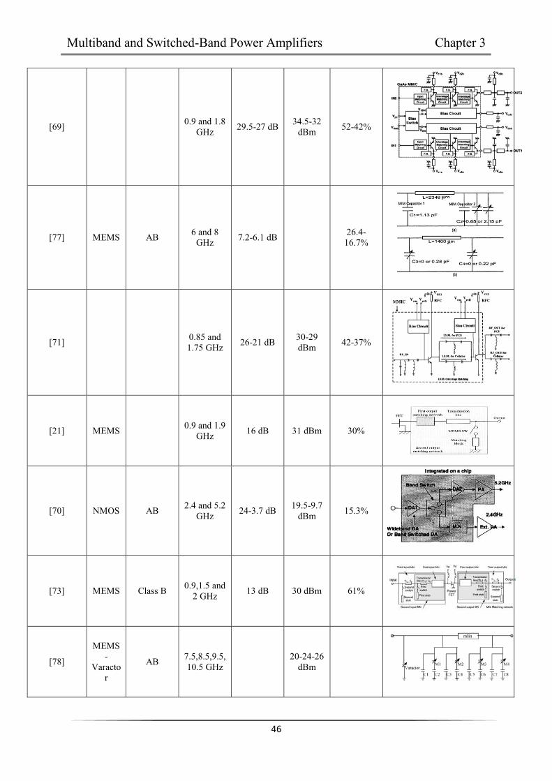
Multiband and Switched-Band Power Amplifiers Chapter 3
46
[69] 0.9 and 1.8 GHz 29.5-27 dB 34.5-32
dBm 52-42%
[77] MEMS AB 6 and 8 GHz 7.2-6.1 dB 26.4-
16.7%
[71] 0.85 and 1.75 GHz 26-21 dB 30-29
dBm 42-37%
[21] MEMS 0.9 and 1.9 GHz 16 dB 31 dBm 30%
[70] NMOS AB 2.4 and 5.2 GHz 24-3.7 dB 19.5-9.7
dBm 15.3%
[73] MEMS Class B 0.9,1.5 and 2 GHz 13 dB 30 dBm 61%
[78]
MEMS-
Varactor
AB 7.5,8.5,9.5, 10.5 GHz 20-24-26
dBm

Multiband and Switched-Band Power Amplifiers Chapter 3
47
[84] PIN diode AB 0.9 and 1.8
GHz 27 dB 30 dBm 40%
[28] Varactor AB
0.9, 1.8, 1.9 and 2.1
GHz 15 dB 27 dBm
[22] MEMS AB 0.9, 1.5, 2 and 5 GHz
10.7-8.3-8.6-8.1 dB
30.5-31-31- 30.8
dBm
64-58-58-45%
[75] MEMS AB 0.9, 1.5,
1.9 and 2.5 GHz
8.3-8.2-8.4-9.6 dB
30.6 dBm
46-53-43-62%
[79] NMOS 2.4 and 5.2 GHZ
10.4-5.1 dB
13-8.7 dBm
16.2-10.8%
[76] MEMS AB 0.9,1.5,1.9
and 2.6 GHz
8.9-8-8.9 and 9.5 dB
30.4-31-30-30.4
dBm
45-50-44-50%
[81] MEMS E 0.9 and 1.8 GHz 20 dBm
[86] MEMS 0.9 and 1.6 GHz 33-30
dBm 42- 26%

Multiband and Switched-Band Power Amplifiers Chapter 3
48
[90] FET B
0.7, 0.8, 0.9, 1.4, 1.7, 1.8, 1.9, 2.3 and 2.5
GHz
30 dB 34 dBm 40%
[80] BST
Varactor
1.7 and 2.3 GHz 27 dB 24.1
dBm
[87]
PIN diodes
1.4 and 2.5 GHz 28 dB 28 dBm 38%
[82] MOSFET D 0.45 and
0.73 GHz 22.4 dB 18 dBm 50%
[74] PIN diodes 0.9,1.5 and
1.9 GHz 12-20-15
dB
39.1-39.4-40
dBm 64-65-61%
[88] E
1.9,2.3,2.6 and 3.5
GHz
24.2-23.8-
23.4-20.5 dBm
[89] E 1.7 and 2.5 GHz 28-27
dBm 57-61.5%

Multiband and Switched-Band Power Amplifiers Chapter 3
49
[83] D 0.6 and 0.78 GHz 20 dB 16-19
dBm 36.6-
46.6%
3.2 Discussion
Table 3.1 and 3.2 summarise different techniques that have been applied to design MB-PA
and SB-PA. To conclude, MB-PA and SB-PA can be designed by a number of parallel
single-band PAs or with reconfigurable MNs (with or without switch). Fig. 3.7 summarizes
all the techniques with their advantages and disadvantages. MB-PA and SB-PA with parallel
single-band PAs are easy to design. These adaptive PAs require one PA for each band of
operation; lots of components (transistors and MN’s component) are required and make these
PAs large in size and expensive. Implementing lots of components, connection between PAs
and biasing for transistors could increase the amount of loss in these PAs. On top of all these
losses, SB-PA with parallel single-band PAs has one more source of loss; the switches used
for connecting to the desired PA. Designing adaptive PA with reconfigurable MN (MB-MN
or SB-MN) is more efficient, smaller and cheaper. As only one transistor is used in these
adaptive PAs, the number of active devices, components and size is dramatically decreased.
SB-MN can provide theoretically more exact impedances compared to MB-MN and
consequently more output power by applying switches at the cost of introducing more losses
in the circuit.
The lack of study on the efficient approach to design adaptive highly efficient PAs
(switched-mode PAs) motivates the author to do the research on the approaches and evaluate
their performances. Also, developing a methodology with a recursive analytical solution for
improving efficiency of SB-PAs is found to be essential to consider as today’s wireless
communication systems designers are continuously seeking better performances.

50
Adaptive
PA
MB-PA SB-PA
Number of
parallel PAs
Number of
parallel PAs MB-MN SB-MN
Advantages
Advantages
Advantages Advantages
Disadvantages
Disadvantages
Disadvantages Disadvantages
-easy to design -lots of components
-large in size
-expensive
-huge losses
-less number of
components
-small in size
-concurrent
amplification
-limitation in
providing optimum
matching at different
frequencies
-easy to design -lots of components
-large in size
-expensive
-huge losses
-loss from switches
-less number
of components
-small in size
-more accurate
matching
-introducing losses
by applying switches
Figure 3.7-Summary of adaptive PAs

51
Chapter 4
Analysis and Design of Switched-Band Matching Networks for Power Amplifiers
A Matching Network (MN) is mainly to transfer load impedances to the desired source
impedances at the specific frequency. At RF and microwave component level, one of the
challenges is the design of multiband MN (MB-MN). Different circuit topologies are defined
for MNs; such as L-match, quarter-wave transformer, single stub and etc [40]. Some MB-MN
problems are more conveniently solved using networks that include switches to increase the
number of degrees of freedom available. Some of the switched-band MNs (SB-MN) use
switches to change the value of inductance or capacitance to obtain the desired impedance
based on the required operating frequency [28], [81]-[82], [84] and [91]. There are some
reported distributed SB-MNs, such as MNs in [21], [73], [86]-[87] and [92]. In [86] and [87],
two output paths were provided and based on the chosen path the circuit operates at different
frequencies. Another technique for SB-MN was introduced by [21] and [73], which use
switchable stubs to provide optimum matching at different operating frequencies. The SB-
MN in [92] used parallel quarter-wavelength transmission line and PIN diode switches at
both ends of transmission line. This MN is switched to different impedances by providing
different characteristic impedances which are achieved by controlling the switches and
connecting or disconnecting the transmission lines [92]. Switches are the main source of
losses in the SB-MNs and the main concern in designing a SB-MN is to decrease these
losses. In some of these topologies, switches are applied in the main signal path and increase
the overall effect of their losses. The other important concerns in designing SB-MNs are
power handling and size issues that need to be taken into account.

Analysis and Design of Switched-Band MN for PAs Chapter 4
52
The SB-MNs proposed in this chapter address these issues by focusing on stub length
switching, such that all switches are grounded. By designing a MN in such way that the
switches are placed between a point on a stub and the ground, the thermal resistance is
reduced, resulting in lower junction temperatures in semiconductor switches. Lower average
temperatures lead to more reliable operation, and lower temperature excursions reduce the
tendency for memory effects in the non-linear behaviour. This would in turn make artificial
linearization (for example, using pre-distortion) less problematic.
All the presented MNs have been built and tested. The description of all the proposed MNs
is followed in this chapter by an analytical solution and comparison in terms of their accuracy
and size. Multiband MNs for PAs is an important research area and needs very precise design
due to the difficulty in managing optimum impedance matching and harmonics termination at
the same time in each band. In the last section, the presented SB-MN is composed of two
blocks, one for optimum matching at fundamental frequency and one for providing open or
short circuit at harmonic frequencies.
4.1 Detach Stub Matching Network
The employed MN is based on the concept which is used in [21]. This MN composed of
two transmission line and two stubs, as shown in Fig. 4.1. The first stub is fixed and the
second one is connected by a switch, and called Detach Stub MN. With the switch OFF, the
MN provides a required impedance at the first required frequency (𝑓1) and in ON state of the
switch (second stub introduced into the circuit), the desired impedance at the second
frequency (𝑓2) is met.

Analysis and Design of Switched-Band MN for PAs Chapter 4
53
4.1.1 Analytical solution
The derived analytical solution of the detach stub MN provides values for the length of the
transmission lines and stubs to give more precise results and shorten the design stage.
a
b
c d
SWPORT 1 PORT 2
1TL 2TL
1S 2S
Figure 4.1- Detached stub matching network
Furthermore, such a solution will help circuit designers to arrive at optimum SB-MNs in a
shorter time. Mainly, the analytical solution is helpful to find any forbidden region for this
MN. The area on the Smith Chart which is unable to be matched with the particular MN
circuit is called ‘Forbidden region’. The equations are derived for ideal and physical
transmission lines with effective dielectric constant (𝜀𝑟).
The ideal transmission line is utilised to prove the possibility of using an analytical
solution. The whole idea of this method is to match by aid of a designated transmission line
and a stub for each frequency. The transmission line 1TL of length 𝑙 provides admittance
𝑌0 + 𝑗𝐵 at point ‘a’ and 𝑗𝐵 is eliminated by introducing the susceptance of an open stub ( 1S ).
The required impedance looking into 1TL at port 1 at the first frequency is 𝑍𝐿1and defined
as 𝑅𝐿1 + 𝑗𝑋𝐿1. At point ‘a’, admittance (𝑌1) can be written as:
𝑌1 = 𝑌0
𝑍0 − 𝑋𝐿1 tan 𝜃𝐿1 + 𝑗𝑅𝐿1 tan 𝜃𝐿1
𝑅𝐿1 + 𝑗(𝑋𝐿1 + 𝑍0 tan 𝜃𝐿1) (4.1)
where 𝑍0 and 𝜃𝐿1 are the characteristic impedance and the electrical length of 1TL ,
respectively. Splitting 𝑌1 into real part and imaginary part yields (4.2) and (4.3) respectively.

Analysis and Design of Switched-Band MN for PAs Chapter 4
54
𝑅𝑒(𝑌1) =𝑅𝐿1(1 + tan2 𝜃𝐿1)
𝑅𝐿12 + (𝑋𝐿1 + 𝑍0𝑡𝑎𝑛𝜃𝐿1)2
(4.2)
𝐼𝑚(𝑌1) =𝑅𝐿1
2 𝑡𝑎𝑛𝜃𝐿1 − (𝑍0 − 𝑋𝐿1𝑡𝑎𝑛𝜃𝐿1)(𝑋𝐿1 + 𝑍0𝑡𝑎𝑛𝜃𝐿1)
𝑍0[𝑅𝐿12 + (𝑋𝐿1 + 𝑍0𝑡𝑎𝑛𝜃𝐿1)2]
(4.3)
Given that the real part of 𝑌1 is equal to the characteristic admittance of the system, 𝑌0, the
electrical length of the transmission line can be obtained by the following equation.
θL1 = tan−1 (𝑋𝐿1 − √𝑅𝐿1[(𝑍0 − 𝑅𝐿1)2 + 𝑋𝐿1
2 ]/𝑍0
𝑅𝐿1 − 𝑍0 ) (4.4)
By substituting 𝜃𝐿1value back into (4.3), the susceptance part of 𝑌1, 𝐵, can be obtained. The
admittance at ‘b’ in Fig. 4.1 is 𝑗𝑌0𝑡𝑎𝑛𝜃𝑆1 and electrical length of the stub ( 1S ) should be
found to eliminate the susceptance of 1Y . So the electrical length of the stub can be calculated
by:
𝜃𝑆1 = tan−1(𝐵
𝑌0) (4.5)
To provide the desired impedance 𝑍𝐿2 = 𝑅𝐿2 + 𝑗𝑋𝐿2 at 𝑓2 , the second stub is introduced
into the circuit by turning the switch ON. To calculate the length of the second transmission
line and stub ( 2TL and 2S respectively), the admittance at ‘c’ (𝑌3) is calculated by (4.6).
𝑌3 = 𝑌0
𝑍0 − 𝑋𝐿2 tan(𝜃𝐿1′ ) + 𝑗𝑅𝐿2 tan(𝜃𝐿1
′ )
𝑅𝐿2 + 𝑗(Z0tan(𝜃𝐿1′ ) + 𝑋𝐿2)
+ 𝑗 Y0tan(𝜃𝑠1′ ) (4.6)
The physical length of 𝑇𝐿1 and 𝑆1 are fixed but their electrical lengths vary as the
frequency changes; therefore, 𝜃𝐿1′ and 𝜃𝑠1
′ are introduced which are the electrical length of the

Analysis and Design of Switched-Band MN for PAs Chapter 4
55
first transmission line and stub at 𝑓2, respectively. Following the same procedure by applying
1/𝑌3 instead of 𝑍𝐿1∗ , we can calculate the electrical lengths of 𝑇𝐿2 and 𝑆2 . The derived
analytical solution is also applicable for SB-MNs covering more than two bands. This can be
done by adding additional switched stubs, positioned relative to 𝑆1, by repeated application of
(4.6) and back to (4.3)-(4.5).
For practical applications, the above introduced algorithm needs to be implemented in a
physical transmission line medium such as microstrip. To find the lengths of transmission
lines and stubs in microstrip, the physical lengths need to be divided by √𝜀𝑒 yielding (4.7)
where 𝜀𝑒 denotes effective dielectric constant.
𝑙 =𝜃. 𝑐
√𝜀𝑒2𝜋𝑓 (4.7)
4.1.2 Numerical Example
To verify the presented approach, the equations have been applied to several different
numerical values in different ranges of frequencies and one of them is presented in this
section. A Gallium Nitride High Electron Mobility Transistor (GaN HEMT) from Nitronex is
chosen as an example. Two different frequencies are selected and appropriate impedances are
obtained from load pull information in the device datasheet. Load pull analysis is a graphical
technique, generating a set of contours on the Smith chart of required impedances for DUT to
achieve specific performances. These contours represent the impedance loci for given
performance parameters for the PA and they are obtained by varying the impedances and
measuring the performance of the PA (output power, gain and efficiency) [94]. The required
normalized impedances are 0.49 + 𝑗0.366 and 1.052 + 𝑗0.456 at 1800 and 900 MHz ,
respectively, with the bandwidth of 400 MHz. The required impedance for the higher
frequency is provided by the OFF state of the switch, since the amount of loss in switch in its

Analysis and Design of Switched-Band MN for PAs Chapter 4
56
ON state increases at higher frequency. Appropriate lengths for the transmission lines and
stubs are calculated in two different versions, ideal and physical transmission lines.
4.1.2.1 Ideal Transmission Line
Using (4.3-4.5) the value of 𝐵, 𝜃𝐿1and 𝜃𝑆1are calculated respectively. In the next step 𝑌3 is
obtained using (4.6). Using the same procedure 𝜃𝐿2 and 𝜃𝑆2 are calculated. These results are
used in the simulation and the results are shown in Fig. 4.2. Good agreement between the
simulation results and the required impedances taken from the device datasheet has been
confirmed.
Figure 4.2-Simulation result of detach stub MN with ideal transmission line
In the first frequency, one transmission line and one stub is used to match to the required
impedance. The second desired impedance is converted to 𝑌3 at point ‘c’ in Fig. 4.1. The
second transmission line and stub parameters are calculated to transform 𝑌3 at the second
frequency to 𝑌0 at points ‘c’ and ‘d’, respectively. No further iteration of the first line and
stub are required to achieve this. The presented method proves that there is no forbidden
region to match any dual frequencies by this MN, because whatever the value of 𝑌3, it can, in
principle, be matched using a single line and stub.

Analysis and Design of Switched-Band MN for PAs Chapter 4
57
4.1.2.2 Physical Transmission Line
The electrical lengths of the transmission lines and stubs in this case are evaluated as
before and their physical lengths are found by use of (4.7). Fig. 4.3 shows the simulation
results based on the calculated lengths with physical transmission line and stubs.
Figure 4.3-Simulation result of detach stub MN with physical transmission line
The results show a perfect match at 1800MHz and a reasonably close match at 900MHz.
The reason for the difference observed in the second frequency is the discontinuity of the T-
junction. Discontinuities are abrupt changes in geometry of microstrip lines which alter the
electromagnetic wave propagation down the line. Some of the common microstrip
discontinuity are open-ends, steps, T-junction and cross junctions. As the reference plane is
shifted by the junction, so by adjusting the length of the transmission line and the stub, the
discontinuity effect of the T-junction can be compensated as shown in [93] and [95]. Taking
into account the discontinuity and fine tuning the simulation will give the result presented in
Fig. 4.4 that shows good agreement at 900 MHz.

Analysis and Design of Switched-Band MN for PAs Chapter 4
58
Figure 4.4-Simulation result after adjustments at the first band
A PIN diode is applied as the switch in all the presented MNs in this work because of its
advantages such as low insertion loss, high isolation, high switching speed and excellent
power handling at microwave frequencies [24]. Two PIN diodes from two different
companies have been selected:
Silicon PIN diode from Infineon (BAR50)
Silicon PIN diode from Skyworks (SMP1302-085LF)
The detach stub MN has been tested with both of these PIN diodes and their result have
been analyzed. The simulation results obtained from both models are satisfactory in terms of
providing appropriate impedance at the output port of the transistor. Dissipation of power in
the PIN diode will consequently introduce loss in the MN. Hence, to choose the best design,
loss in the circuit should be minimized. The loss of these MNs are analysed by aid of the
definition of total loss factor which is based on the concept of energy conservation. A loss
factor can be derived by studying the total power emerging from the network in response to
an input at one port. On this basis, the loss factor has been derived as:
221
2
11 SSLoss (4.8)
Where a value of one indicates a lossless circuit and a value less than one shows that there
is loss. The simulated values of this equation for both MN with two PIN diodes are plotted in

Analysis and Design of Switched-Band MN for PAs Chapter 4
59
the following two graphs, Fig. 4.5. The result desired to be close to one and minimise the
losses introduced by PIN diode into the circuits.
Comparing both results presented in Fig. 4.5, Infineon PIN diode gives better results for
both frequencies with total loss factor very close to one while Skyworks gives a lower total
loss factor. Obviously, the first model has less loss and dissipates less power in the MN.
(a) (b)
Figure 4.5-Total loss factor of the detach stub MN in OFF (blue) and ON (pink) state with PIN diode (a) Infineon and (b) Skyworks
4.1.3 Experimental Result
The MN based on the calculation in the previous section has been built, to prove the
validation of the algorithm. It was fabricated on Microstrip substrate of thickness of 0.76 mm
and relative dielectric constant of 3.5. The PIN diode, as mentioned earlier, is type BAR50
from Infineon.
The simulation and measurement results are compared and plotted by their magnitude
(Fig. 4.6) and on the Smith Chart (Fig. 4.7). The markers on Fig. 4.7 ((a) and (b)) indicate the
reflection coefficient at the intended frequencies for the ON and OFF state (1800 and 900
MHZ, respectively). Both graphs show good agreement between simulation and
measurement. The small differences are due to real components and their tolerances.
500 1000 1500 2000
Frequency (MHz)
Loss Infineon
0.7
0.75
0.8
0.85
0.9
0.95
1
900 MHz0.9553
1800 MHz0.97644
|Eqn(Loss1)|Output Equations1
|Eqn(Loss2)|Output Equations1
500 1000 1500 2000
Frequency (MHz)
Loss Skywork
0.7
0.75
0.8
0.85
0.9
0.95
1
900 MHz0.92049
1800 MHz0.94867
|Eqn(Loss3)|Output Equations1
|Eqn(Loss4)|Output Equations1
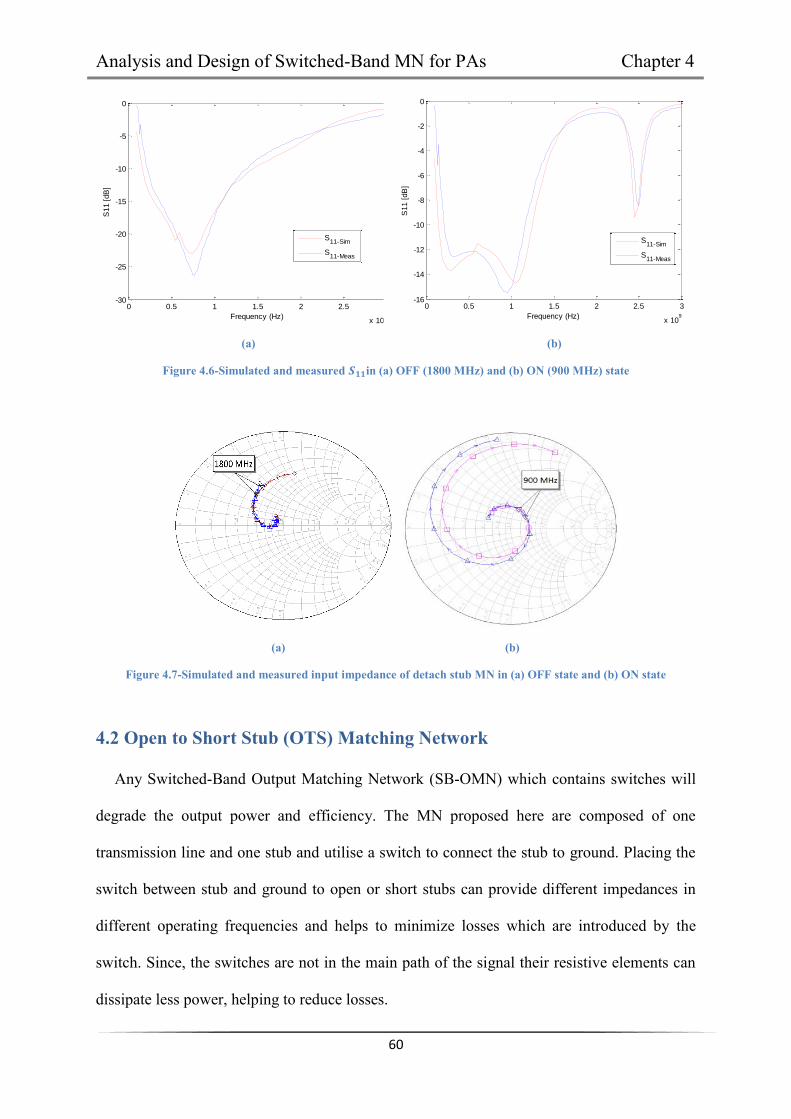
Analysis and Design of Switched-Band MN for PAs Chapter 4
60
(a) (b)
Figure 4.6-Simulated and measured 𝑺𝟏𝟏in (a) OFF (1800 MHz) and (b) ON (900 MHz) state
(a) (b)
Figure 4.7-Simulated and measured input impedance of detach stub MN in (a) OFF state and (b) ON state
4.2 Open to Short Stub (OTS) Matching Network
Any Switched-Band Output Matching Network (SB-OMN) which contains switches will
degrade the output power and efficiency. The MN proposed here are composed of one
transmission line and one stub and utilise a switch to connect the stub to ground. Placing the
switch between stub and ground to open or short stubs can provide different impedances in
different operating frequencies and helps to minimize losses which are introduced by the
switch. Since, the switches are not in the main path of the signal their resistive elements can
dissipate less power, helping to reduce losses.
0 0.5 1 1.5 2 2.5 3
x 109
-30
-25
-20
-15
-10
-5
0
Frequency (Hz)
S11 [
dB
]
S11-Sim
S11-Meas
0 0.5 1 1.5 2 2.5 3
x 109
-16
-14
-12
-10
-8
-6
-4
-2
0
Frequency (Hz)
S11 [
dB
]
S11-Sim
S11-Meas

Analysis and Design of Switched-Band MN for PAs Chapter 4
61
4.2.1 Design
The whole idea of this MN is to provide required impedances by a single stub and varies
in two different frequencies by aid of a switch at the end of the stub to obtain open- or short-
circuit stub. This is referred to as Open to Short MN (OTS) (Fig 4.8). The ON state of the
switch provides a short stub at the lower frequency and the stub is open when the switch is
OFF, for the higher frequencies use. The length and the characteristic impedance of the
transmission line and the stub are optimized to provide required impedances at the specific
frequencies.
TL1
S1
PORT 1 PORT 2
SW
a
Figure 4.8-Open to Short MN
4.2.2 Analytical solution
In OTS, only one transmission line and stub are available to adjust their length and
characteristic impedance to achieve desired impedance at both operating frequencies.
Generally, the method of the OTS MN is to suppose the required impedances are presented at
‘port 1’ and aim to provide the system impedance at ‘port 2’ by aid of a transmission line and
a stub. The steps that have been followed to derive an analytical solution for this MN are:
Suppose required impedances at both bands are provided at ‘port 1’
Adjust length and characteristic impedance of the transmission line to present
10 jBY at 1f and 20 jBY at 2f
Eliminate 1jB by appropriate length and width of short-circuited stub

Analysis and Design of Switched-Band MN for PAs Chapter 4
62
Eliminate 2jB by appropriate length and width of open-circuited stub
The aim of deriving the analytical solution is to be able to calculate length and
characteristic impedance of the transmission line ( 1TL ) and stub ( 1S ) accurately. The physical
lengths of the transmission line for both frequencies have been derived the same way as
explained in section 4.1.1. Practically, both physical lengths should be the same as they refer
to the same transmission line, (4.9).
12
22
221
1
2L2
1
211
21
211
1
1L1
1
1
])()[(X-tan1
])()[(X-tan1
ZR
XRZZR
fZR
XRZZR
f L
LLL
L
LLL
(4.9)
where the required impedances are 111 LLL jXRZ and 222 LLL jXRZ for the first ( 1f )
and second ( 2f ) band which are known values. 1Z is the characteristic impedance of 1TL and
is unknown. Both sides of equation (4.9) include 1tan with different coefficients (1
1f
and
2
1f
) and they cannot be equal for a particular 1Z and any 1LZ and 2LZ . Therefore, this MN
has forbidden region. In order to find an analytical solution and define the coverage region of
the OTS MN, different special cases need to be considered.
To begin with, the assumption has been made that the transmission line is quarter
wavelength at 1f . So, the length of the transmission line in air space is22 1e
1
fcL . The
admittance at point ‘a’ is 21
11
ZjXR LL . The conductance should be equal to the normalized
Analysis and Design of Switched-Band MN for PAs Chapter 4
63
system admittance and therefore, 11 LRZ . The switch is ON when the circuit is operating
at the first frequency and the length of the short-circuited stub can be found by:
21
11
12 tan
2 ZXR
fcL
L
L
e (4.10)
There are two unknowns in (4.10), length ( 2L ) and characteristic impedance ( 2Z ) of the
stub. To be able to find unique values for 2L and 2Z , another equation for 2L is needed at the
second frequency. The physical length of the transmission line is obtained and the electrical
length of the transmission line in the second band ( 2L ) can be found by 21
2
ff . Three
different cases are going to analyze:
Case 1: 1
2
ff =even integer number nL 2
Case 2: 1
2
ff =odd integer number
22
nL
Case 3: 1
2
ff =any value 2L any value
In case 1, 2tan L is zero and the admittance at point ‘a’ for the second band is
22
22
22
LL
LL
XRjXR
. The normalized conductance should be unity to meet the system impedance at
‘port 2’. To satisfy this, the length and width of transmission line would need to be adjusted.
However, they had been calculated earlier to meet the first band requirement and they are
fixed. Therefore, the only way to meet this condition (the normalized conductance to be
unity) is 2LX should be 222 LL RR . At the second band, the switch is OFF and the stub is
open. Length of the stub can be found by:

Analysis and Design of Switched-Band MN for PAs Chapter 4
64
22
22
221
22 tan
2 LL
L
e XRZX
fcL
(4.11)
2Z and 2L are unknown in (4.11) like (4.10). Now there are two equations and two
unknowns and this can be easily solved. This has been done in this work by finding 2L with
substituting different value of 2Z in an acceptable range. Different values for 2L have been
obtained from (4.10) and (4.11) and they are plotted in the same graph with respect to 2Z in
order to find the crossing point, which identifies the appropriate values.
According to the equations, this MN with frequency condition of 1
2
ff =even integer
number can be applied for the certain output impedances for which they met the conditions.
These conditions are:
2222 LLL RRX
12 LR
MATLAB has been used to find the coverage region of the OTS MN in the first case. All
the conditions have been applied in MATLAB to locate the impedances on the Smith chart.
The impedances for which OTS MN can be designed are shown in Fig. 4.9(a), the blue dots
show 1LZ and red dots show 2LZ . The reason that they are only capacitive loads for 1LZ is that
(4.10) results in a negative length when inductive loads applied and need to add quarter
wavelength to the stub and in that case the stubs cannot have the same physical length for
both bands of operation. To be able to match inductive loads as well we need to shift
switching condition in the frequencies: the ON state of the switch at the higher band and the
OFF state at the lower band of operation. The equation for calculating length of the stub will
be:

Analysis and Design of Switched-Band MN for PAs Chapter 4
65
1
211
121 tan
2 L
L
e RZX
fcL
(4.12)
22
22
221
222 tan
2 ZXXR
fcL
L
LL
e (4.13)
21L and 22L are the length of stub at first and second frequency, respectively. The coverage
region in this case has been analyzed in MATLAB and plotted the impedances on the Smith
chart in Fig. 4.9(b).
(a) (b)
Figure 4.9-Coverage region of OTS in case 1(a) capacitive load and (b) inductive load
The second case is when the ratio of the frequencies is an odd integer number. The
admittance at point ‘a’ in Fig. 4.8 for the second bands is 21
222 Z
jXRY LL . To provide the
system impedance at ‘port 2’ 1Z should be equal to 2LR . The characteristic impedance of
the transmission line ( 1Z ) at the first band has been calculated to be 1LR ; therefore, 1LR has
to be equal to 2LR . At the second frequency, the switch is OFF and the stub is open, so the
length of the stub can be calculated by:
0.2
0.5
1.0
2.0
5.0
+j0.2
-j0.2
+j0.5
-j0.5
+j1.0
-j1.0
+j2.0
-j2.0
+j5.0
-j5.0
0.0
0.2
0.5
1.0
2.0
5.0
+j0.2
-j0.2
+j0.5
-j0.5
+j1.0
-j1.0
+j2.0
-j2.0
+j5.0
-j5.0
0.0

Analysis and Design of Switched-Band MN for PAs Chapter 4
66
2
221
22 tan
2 L
L
e RZX
fcL
(4.14)
The same technique is applied here to plot both 2L from (4.10) and (4.14) in the same
graph and find 2Z and 2L . The only condition applied in this case is the same resistance for
both required impedances. Fig. 4.10 is shown the coverage region of OTS in case 2 that
obtained in MATLAB.
Figure4.10-Coverage region for OTS in case 2
The next step is analyzing the third case. By assuming the required impedance at ‘port 1’
in the second band of operation, the input impedance at point ‘a’ can be written as:
22211
21221
*2 tantan
tan
LLLL
LLL
jRXZZXjRZZ
(4.15)
Then the conductance is found:
2
2122
2
22
2*2 tan
tan1)Re(LLL
LL
ZXRRY
(4.16)
0.2
0.5
1.0
2.0
5.0
+j0.2
-j0.2
+j0.5
-j0.5
+j1.0
-j1.0
+j2.0
-j2.0
+j5.0
-j5.0
0.0

Analysis and Design of Switched-Band MN for PAs Chapter 4
67
Equation (4.16) needs to have specific values for 2LR and 2LX to be equal to one. The
length of the stub in ON state of the switch (short-circuited stub) and OFF state (open-circuit
stun) can be found by (4.10) and (4.17):
21
22 tan
2BZ
fcL
(4.17)
B is the susceptance of *2Y . 2Z and 2L can be found by plotting both equations ((4.10) and
(4.17)) in one graph with respect to different value of 2Z . The coverage region of the OTS in
third case is shown in Fig.4.11. According to Fig.4.9, 4.10 and 4.11, this MN results in a poor
coverage region of the Smith chart. Therefore, this MN is not able to work over a wide range
of frequencies and achieve any required impedances due to having too few adjustable
elements.
Figure 4.11-Coverage region for OTS in third case
4.2.3 Numerical Example
To verify the technique explained in the previous section, three numerical examples for
each case are presented here. Two frequencies and their required impedances have been
chosen. The first example is for case 1 where the second frequency is twice of the first
0.2
0.5
1.0
2.0
5.0
+j0.2
-j0.2
+j0.5
-j0.5
+j1.0
-j1.0
+j2.0
-j2.0
+j5.0
-j5.0
0.0

Analysis and Design of Switched-Band MN for PAs Chapter 4
68
frequency, 900MHz and 1800MHz. The aim is to provide 456.0052.1 j and 366.049.0 j
at ‘port 1’ in the first and second band, respectively. Electrical length of 2 and at the first
and second band results in physical length of 50mm. The normalized characteristic
impedance of the transmission line is 052.1 , so the width of the transmission line will be
1.61mm. Equations (4.12) and (4.13) have been used to find the length of the stub for both
frequencies by substituting different values of 2Z . The logical values for normalized 2Z is
between 0.4 and 1.8, according to the substrate and the feasible width. The two stub lengths
are plotted in the same graph, Fig. 4.12. In this figure, red line shows 2L for the first band
and blue is for the second band.
In Fig. 4.12, the point that stub has the same length in both frequencies has been marked.
Therefore, width of 1.73mm and length of 11.4mm have been chosen for the stub. These
values are applied in the simulation and the simulation results are shown in Fig. 4.13.
The second example (case 2) is for 0.9GHz and 2.7GHz and their required impedances are
1.14.01 jZL and 8.04.02 jZL , respectively. The characteristics impedance of the
transmission line is 4.01 Z . The electrical length of the transmission line ( 1TL ) at the first
band is21
L which is 2
32
L at the second band and its physical length is 48.73mm. To
find the length and characteristics impedance of the stub, equation (4.10) and (4.14) are
plotted in Fig. 4.14. At normalized 2Z equal to 0.96 both stub length have the same value
which is 10.3mm. The simulation results with these values are shown in Fig. 4.15. These
results show a good match with the required impedances at both bands.

Analysis and Design of Switched-Band MN for PAs Chapter 4
69
Figure 4.12-Physical length of the stub with different characteristics impedance
(a) (b)
Figure 4.13-Simulation result of OTS in case 1 (a) OFF and (b) ON state of the switch
0.4 0.6 0.8 1 1.2 1.4 1.6 1.80.004
0.006
0.008
0.01
0.012
0.014
0.016
0.018
0.02
X: 0.98
Y: 0.01143
Normalized Z2
Physic
al le
ngth
of
stu
b (
m)
0 1.0
1.0
-1.0
10.0
10.0
-10.0
5.0
5.0
-5.0
2.0
2.0
-2.0
3.0
3.0
-3.0
4.0
4.0
-4.0
0.2
0.2
-0.2
0.4
0.4
-0.4
0.6
0.6
-0.6
0.8
0.8
-0.8
OTSSwp Max
1200MHz
Swp Min
700MHz
900 MHzr 1.06975x 0.377768
S(1,1)
OTS
0 1.0
1.0
-1.0
10.0
10.0
-10.0
5.0
5.0
-5.0
2.0
2.0
-2.0
3.0
3.0
-3.0
4.0
4.0
-4.0
0.2
0.2
-0.2
0.4
0.4
-0.4
0.6
0.6
-0.6
0.8
0.8
-0.8
OTSSwp Max
1900MHz
Swp Min
1700MHz
1800 MHzr 0.433278x 0.531834
S(1,1)
OTS

Analysis and Design of Switched-Band MN for PAs Chapter 4
70
Figure 4.14- Physical length of the stub for different characteristics impedance of the stub
(a) (b)
Figure 4.15- Simulation result of OTS MN in case 2 (a) ON state and (b) OFF state
The two required impedances chosen for the example of the case 3 are 6.05.01 jZL at
900MHz and 75.03.02 jZL at 2000MHz. The normalized characteristics impedance of the
first transmission line is found as 0.7 which result in 2.84mm width. The length of the
transmission line is 50.7mm. The same process as two previous examples are followed here
0.4 0.6 0.8 1 1.2 1.4 1.6 1.80.004
0.006
0.008
0.01
0.012
0.014
0.016
0.018
0.02
X: 0.96
Y: 0.01031
Normaluzed Z2
Physic
al le
ngth
of
the s
tub (
m)
0 1.0
1.0
-1.0
10.0
10.0
-10.0
5.0
5.0
-5.0
2.0
2.0
-2.0
3.0
3.0
-3.0
4.0
4.0
-4.0
0.2
0.2
-0.2
0.4
0.4
-0.4
0.6
0.6
-0.6
0.8
0.8
-0.8
Graph 1Swp Max
1000MHz
Swp Min
800MHz
900 MHzr 0.373677x -1.16444
S(1,1)
Schematic 1
0 1.0
1.0
-1.0
10.0
10.0
-10.0
5.0
5.0
-5.0
2.0
2.0
-2.0
3.0
3.0
-3.0
4.0
4.0
-4.0
0.2
0.2
-0.2
0.4
0.4
-0.4
0.6
0.6
-0.6
0.8
0.8
-0.8
Graph 1Swp Max
2800MHz
Swp Min
2500MHz
2700 MHzr 0.496205x 0.813978
S(1,1)Schematic 1

Analysis and Design of Switched-Band MN for PAs Chapter 4
71
and equation (4.10) and (4.17) are plotted in Fig. 4.16. The normalized optimum
characteristic impedance of 0.47 and the length of 29.8mm are found.
Figure 4.16-Physical length of the stub for different characteristics impedance of the stub
These calculated values are applied in simulation to prove the validity of this algorithm.
The simulation results (Fig. 4.17) are shown reasonably close match to the required
impedances.
(a) (b)
Figure 4.17-Simulation result of OTS MN in case 3 (a) ON state and (b) OFF state
The loss of the OTS MN has been analyzed to prove the improvement in minimizing the
loss of OTS MN compare to the detach stub MN. Fig. 4.18 illustrates the loss introduced by
0.2 0.4 0.6 0.8 1 1.2 1.4 1.6 1.80.01
0.015
0.02
0.025
0.03
0.035
0.04
0.045
X: 0.47
Y: 0.02988
Normalized Z2
Physic
al le
ngth
of
stu
b (
m)
0 1.0
1.0
-1.0
10.0
10.0
-10.0
5.0
5.0
-5.0
2.0
2.0
-2.0
3.0
3.0
-3.0
4.0
4.0
-4.0
0.2
0.2
-0.2
0.4
0.4
-0.4
0.6
0.6
-0.6
0.8
0.8
-0.8
OTSSwp Max
1000MHz
Swp Min
800MHz
900 MHzr 0.585801x -0.620364
S(1,1)
OTS
0 1.0
1.0
-1.0
10.0
10.0
-10.0
5.0
5.0
-5.0
2.0
2.0
-2.0
3.0
3.0
-3.0
4.0
4.0
-4.0
0.2
0.2
-0.2
0.4
0.4
-0.4
0.6
0.6
-0.6
0.8
0.8
-0.8
OTSSwp Max
2100MHz
Swp Min
1900MHz
2000 MHzr 0.306086x 0.570715
S(1,1)
OTS

Analysis and Design of Switched-Band MN for PAs Chapter 4
72
the switch to this MN. As shown in the graph, the losses at both states (ON and OFF) of the
switch are very close to one. In ON state of the switch, 3% improvement has been achieved.
Figure 4.18-Total loss factor of the switch in the OTS MN in OFF state (blue) and ON state (pink)
4.2.4 Experimental
The OTS MN (the case 1) has been fabricated to verify the methods, Fig. 4.19. The PIN
diode has been biased with a capacitor and a resistor. The applied voltage is 8 V and the
voltage after the PIN diode will be 7.3 V due to the PIN diode forward voltage drop.
Therefore, the value of the resistor can be calculated to conduct forward current of 10 mA. A
capacitor is used to provide RF ground and low reactance at the intended frequency (same
value as DC blocking capacitor, i.e. 47 pF). The simulation and measurement results are
compared and plotted on the Smith Chart (Fig 4.20). The experimental results are reasonably
close to the simulations and validate the analytical solution and that by switching the stub to
the ground is capable of providing the required impedance in the other frequency band.
Figure 4.3-Photograph of OTS MN (switch end of the stub)
500 1000 1500 2000
Frequency (MHz)
Loss OTS
0.7
0.75
0.8
0.85
0.9
0.95
1
900 MHz0.98409
1800 MHz0.97695
|Eqn(Loss7)|Output Equations1
|Eqn(Loss8)|Output Equations1

Analysis and Design of Switched-Band MN for PAs Chapter 4
73
(a) (b)
Figure 4.20-Simulated and measured input impedance of OTS MN at (a) ON state and (b) OFF state
4.3 Short to Stub (STS) Matching Networks
The presented MN in this section is a single stub MN and a different matching condition is
provided by using a stub which can be adjusted in length and width and made either open- or
short-circuit. To make this possible, the position and mode of the switch is altered and it
provides different performances.
4.3.1 Design
In the method called Stub to Short switching (STS), the switch is situated somewhere in
middle of the stub (Fig 4.21). When the switch is ON, the stub is shorter and is grounded. The
longer and open stub is provided in the OFF state of the switch. Typically, the higher
frequency needs shorter stub rather than the lower frequency; therefore, ON state of the
switch is applied at higher frequency. By optimizing the length and characteristic impedance
of the transmission line and stub, optimum matching can be provided at different frequencies.
S1
S2
TL1
PORT 1 PORT 2
SW
a
b
Figure 4.4-Stub to Short MN

Analysis and Design of Switched-Band MN for PAs Chapter 4
74
By using the switch in the middle of the stub, in STS, one longer stub is used in one of the
frequencies and an extra degree of freedom is provided to design; therefore, more frequencies
can be covered by this method.
4.3.2 Analytical solution
As for the other two MNs (detach stub and OTS MN), an analytical solution is derived for
this MN. The reason to derive equation is not only making the designing MN in the shorter
time and more accurate result, but also to discover any forbidden region for this MN. For the
start, the electrical length of the transmission line is assumed to be quarter wavelength at first
band. The input admittance at point ‘a’ in Fig. 4.21 is 21
11
ZjXR LL , where 1LR and 1LX are the
resistance and reactance of the required impedance at the first band and 1Z is the
characteristic impedance of the transmission line. The characteristic impedance of the
transmission line is calculated to be 1LR to provide 1
10
L
L
RXjY at ‘port 2’. At the first band
the switch is OFF and both stubs are connected. To find the susceptance of the stub at point
‘a’, first need to find the impedance at point ‘b’:
21
3"1 tan S
ZjZ
(4.18)
"1Z and 3Z are impedance at point ‘b’ and characteristic impedance of the second stub,
respectively and 21S is electrical length of the second stub at the first band. Then the
susceptance at point ‘a’ can be found by:
211123
1132121 tantan
tantan
SS
SS
ZZZZjB
(4.19)

Analysis and Design of Switched-Band MN for PAs Chapter 4
75
11S is the electrical length of the first stub at the first band and 2Z is the characteristic
impedance of the first stub. Then, the length of the second stub is:
2111
2111
2
31
13 tan
tantan2 SLL
SLL
e XRRX
ZZ
fcL
(4.20)
This equation has four unknowns and makes it impossible to solve. When the switch is
ON, the first stub is connected to the ground and the second stub is out of the circuit. In the
ON state of the switch, the length and width of the first stub can be found to decrease the
number of unknowns in (4.20). The electrical length of the transmission line at the second
band is 21
2
ff . Three cases are going to analyze, same as the OTS MN.
In the first case (1
2
ff is an even integer number), 2tan L is zero and admittance at point ‘a’
is 22
22
22
LL
LL
XRjXR
. The conductance is fixed and the only way to provide 22
22
20
LL
L
XRXjY
at
‘port 2’ is, 2LX to be equal to 222 LL RR . The switch is ON and the length of the first stub
can be found by:
22
22
221
22 tan
2 ZXXR
fcL
L
LL
e (4.21)
Any value of 2Z can be chosen and the length of the stub can be found accordingly. By
replacing these values back to the equation (4.20), a value of 3Z can be chosen and find the
length of the second stub. The only condition applied for this case is the value for reactance
of the second impedance ( 2222 LLL RRX ). Fig. 4.22 illustrates the acceptable values for
2LZ . There is no condition for the impedance at the first band and it can have any values.

Analysis and Design of Switched-Band MN for PAs Chapter 4
76
Figure 4.5-Coverage region for STS MN in case 1
The second case is when the ratio of the frequencies is an odd integer number. By
considering that 2tan L (is the electrical length of the transmission line at the second
frequency) is going to infinity, then the admittance at point ‘a’ is 21
22
ZjXR LL
. The
characteristic impedance of the transmission line can be found by 21 LRZ . For the first
band of operation, 1Z has been found as 1LR . The only condition allow this case to be valid
is 21 LL RR . The switch in ON for the second band and the first stub is just connected to the
circuit; therefore, the length of the first stub is:
22
21
22 tan
2 ZXR
fcL
L
L
e (4.22)
The same process applied here, the width and the length of the first stub can be calculated
by aid of (4.22). The next step is going back to (4.20) which have two unknowns now; the
length of the second stub can be calculated by selecting an acceptable value for 3Z . As
mentioned earlier, the resistance of both required impedances need to be equal and both of
0.2
0.5
1.0
2.0
5.0
+j0.2
-j0.2
+j0.5
-j0.5
+j1.0
-j1.0
+j2.0
-j2.0
+j5.0
-j5.0
0.0

Analysis and Design of Switched-Band MN for PAs Chapter 4
77
them are equal to 21Z . The STS MN in case 2 can match any impedance on any of the circles
shown in Fig. 4.23.
Figure 4.6-Coverage region for STS MN in case 2
The input impedance at point ‘a’ in the third case is (4.15) and the same condition is
applied as well, which is 1Re *2 Y (equation for *
2Re Y is (4.16)). The required impedance
at the second frequency needs to have suitable value for its resistance and reactance to make
this argument true. The length of the first stub, when the switch is ON at the second
frequency, is:
2
1
22
1tan2 ZBfcL
e (4.23)
B is the susceptance of *2Y . The length and width of both stubs can be calculated by
(4.20) and (4.23). The STS MN has no forbidden region for the required impedance at the
first band, whereas, it is able to operate only in the impedances shown on the Smith chart at
the second band in Fig. 4.24.
0.2
0.5
1.0
2.0
5.0
+j0.2
-j0.2
+j0.5
-j0.5
+j1.0
-j1.0
+j2.0
-j2.0
+j5.0
-j5.0
0.0

Analysis and Design of Switched-Band MN for PAs Chapter 4
78
Figure 4.7-Coverage region of the STS MN in case 3
The STS MN compare to the OTS MN has excellent coverage region based on their
acceptable points on the Smith chart. Finding the characteristic impedance of the stubs are
independent from each other due to providing an additional stub for one band of operation.
4.3.3 Numerical Example
All the presented cases for the STS MN are represented with numerical example in this
section. Table 4.1 illustrates the selected frequencies and their required impedances in each
case.
Table 4.1-Selected frequencies and their required impedances for all the cases
1f 1LZ 2f 2LZ
Case 1 900MHz 45.0052.1 j 1800MHz 49.049.0 j
Case 2 900MHz 35.05.0 j 2700MHz 65.05.0 j
Case 3 782MHz 8.18.0 j 1748MHz 13.09.0 j
0.2
0.5
1.0
2.0
5.0
+j0.2
-j0.2
+j0.5
-j0.5
+j1.0
-j1.0
+j2.0
-j2.0
+j5.0
-j5.0
0.0

Analysis and Design of Switched-Band MN for PAs Chapter 4
79
The length and width of the transmission line and stubs have been calculated by algorithm
presented in the previous section. These values are tabulated in Table 4.2; all the values are in
mm.
Table 4.2-Calculated length and width of the transmission line and stubs for STS MN in all the cases
1L 1W 2L 2W 3L 3W
Case 1 52.7 1.61 8.5 0.5 5.2 0.5
Case 2 52.7 2.83 7.3 1.67 13.1 1.67
Case 3 58.4 2 23.3 0.5 26.1 0.5
The STS MN has been simulated with these values. The simulation result for case1, case 2
and case 3 are shown in Fig. 4.26, 4.27 and 4.28, respectively. The simulation result for all
the cases are shown very well matched to the required impedances.
The loss of the PIN diode in the STS MN has been analyzed and is shown in Fig 4.25.
There is an improvement compare to the detach stub MN and again it is proof that by this
technique the losses of the switch are minimized.
Figure 4.25-Total loss factor analysis of the switch in STS MN in OFF state (blue) and ON state (pink)
500 1000 1500 2000
Frequency (MHz)
Loss STS
0.7
0.75
0.8
0.85
0.9
0.95
1
1800 MHz0.96125
900 MHz0.98248
|Eqn(Loss5)|Output Equations1
|Eqn(Loss6)|Output Equations1

Analysis and Design of Switched-Band MN for PAs Chapter 4
80
(a) (b)
Figure 4.8-Simulation result of the STS MN in case 1 (a) OFF and (b) ON state of the switch
(a) (b)
Figure 4.9-Simulation result of the STS MN in case 2 (a) OFF and (b) ON state of the switch
(a) (b)
Figure 4.10-Simulation result of the STS MN in case 3 (a) OFF and (b) ON state of the switch
0 1.0
1.0
-1.0
10.0
10.0
-10.0
5.0
5.0
-5.0
2.0
2.0
-2.0
3.0
3.0
-3.0
4.0
4.0
-4.0
0.2
0.2
-0.2
0.4
0.4
-0.4
0.6
0.6
-0.6
0.8
0.8
-0.8
STSSwp Max
1000MHz
Swp Min
800MHz
900 MHzr 1.04751x 0.448655
S(1,1)
STS
0 1.0
1.0
-1.0
10.0
10.0
-10.0
5.0
5.0
-5.0
2.0
2.0
-2.0
3.0
3.0
-3.0
4.0
4.0
-4.0
0.2
0.2
-0.2
0.4
0.4
-0.4
0.6
0.6
-0.6
0.8
0.8
-0.8
STSSwp Max
1900MHz
Swp Min
1700MHz
1800 MHzr 0.498296x 0.478436
S(1,1)
STS
0 1.0
1.0
-1.0
10.0
10.0
-10.0
5.0
5.0
-5.0
2.0
2.0
-2.0
3.0
3.0
-3.0
4.0
4.0
-4.0
0.2
0.2
-0.2
0.4
0.4
-0.4
0.6
0.6
-0.6
0.8
0.8
-0.8
STSSwp Max
1000MHz
Swp Min
800MHz
900 MHzr 0.501132x 0.350474
S(1,1)
STS
0 1.0
1.0
-1.0
10.0
10.0
-10.0
5.0
5.0
-5.0
2.0
2.0
-2.0
3.0
3.0
-3.0
4.0
4.0
-4.0
0.2
0.2
-0.2
0.4
0.4
-0.4
0.6
0.6
-0.6
0.8
0.8
-0.8
STSSwp Max
2800MHz
Swp Min
2600MHz
2700 MHzr 0.508163x 0.654318
S(1,1)
STS
0 1.0
1.0
-1.0
10.0
10.0
-10.0
5.0
5.0
-5.0
2.0
2.0
-2.0
3.0
3.0
-3.0
4.0
4.0
-4.0
0.2
0.2
-0.2
0.4
0.4
-0.4
0.6
0.6
-0.6
0.8
0.8
-0.8
STSSwp Max
800MHz
Swp Min
700MHz
782 MHzr 0.833446x 1.84239
S(1,1)
STS
0 1.0
1.0
-1.0
10.0
10.0
-10.0
5.0
5.0
-5.0
2.0
2.0
-2.0
3.0
3.0
-3.0
4.0
4.0
-4.0
0.2
0.2
-0.2
0.4
0.4
-0.4
0.6
0.6
-0.6
0.8
0.8
-0.8
STSSwp Max
1800MHz
Swp Min
1700MHz
1748 MHzr 1.09474x 0.132594
S(1,1)
STS

Analysis and Design of Switched-Band MN for PAs Chapter 4
81
4.3.4 Experimental
The case 1 has been fabricated as an example of the STS MN and it is shown in Fig 4.29.
The experiment results are shown in Fig. 4.30 and they are plotted on the Smith chart with
the simulation result. The measured impedances and the simulation results agree very well
over wide range of frequency. The slight difference between them is due to the variations in
parameters in real components.
Figure 4.11-Photographs of the fabricated STS MN in case 1 (switch in the middle of the stub)
(a) (b)
Figure 4.30-Simulated and measured input impedance of STS MN in case 1 (a) OFF state and (b) ON state
4.4 Comparison of Matching Networks
Three SB-MNs have been presented in the previous sections. The switch is not placed in
the main path of the signal and this is an advantage for all the presented MNs. The last two
MNs (OTS and STS MN) are more preferable than the detach stub MN as they reduced the
losses introduced into the circuit by the switches. These two MNs are compared in terms of
their performances in this section. One of the advantages of the OTS MN over the STS MN is
using ON state of the switch at the lower frequency. But in STS, since the higher frequency

Analysis and Design of Switched-Band MN for PAs Chapter 4
82
requires a shorter stub, the ON state of the switch is used at the higher frequency. Table 4.3
compares these two methods. To compare the accuracy of MNs in achieving desired
impedances, the error in percentages is provided, showing the effect of the limited numbers
of degrees of freedom, in ON and OFF state of the switch. These percentage errors shows the
accuracy of the MNs and are calculated by |𝑑𝑒𝑠𝑖𝑟𝑒𝑑 𝑖𝑚𝑝𝑒𝑑𝑎𝑛𝑐𝑒−𝑜𝑏𝑡𝑎𝑖𝑛𝑒𝑑 𝑖𝑚𝑝𝑒𝑑𝑎𝑛𝑐𝑒
𝑜𝑏𝑡𝑎𝑖𝑛𝑒𝑑 𝑖𝑚𝑝𝑒𝑑𝑎𝑛𝑐𝑒| ∗ 100. The
values in Table 4.3 show that the STS method is more suitable for generating the required
impedances than OTS method. Also, their coverage region on the Smith chart is another
proof that STS MN can operate over wider range of the impedances.
Table 4.3-OTS and STS MN comparison
OTS STS
Size 3.5×3 cm 5×1.8 cm
Limitation degree in ON state 4.1% 2.8%
Limitation degree in OFF state 16.9% 0.3%
ON state of the switch Lower frequency Higher frequency
4.5 Harmonic Termination Network
The MNs which are applied in PAs need proper suppression of harmonics. If a MB-PA
design is required to support several operation bands, harmonics which need to be terminated
will increase and it makes MB-MN even more challenging to design. Impedance Buffer (IB)
elements are used to provide either open or short circuit, as required, by aid of an open or
short circuited shunt stub at harmonic frequencies in [96]. A shunt transmission line with a
capacitor shorted to ground is another technique used by [19] and [23].
High efficiency switching classes of amplifier (Class-E, Class-F, etc) typically require
combinations of open and/or short circuit termination at harmonic frequencies. For example,
the ideal situation for Class-E PA is to have open circuit terminations at the second and

Analysis and Design of Switched-Band MN for PAs Chapter 4
83
higher harmonic frequencies [97]. The second harmonics has been shown to be sufficient for
reasonable approximation to Class-E waveforms. The problem of achieving such harmonic
terminations for two different fundamental frequencies is addressed here.
4.5.1 Theory of Harmonic Termination Network
The basic idea of the proposed Harmonic Termination (HT) network is using a transmission
line and an open stub both with electrical length of 𝜆/4 , (Fig 4.31). Thus this block is
composed of a transmission line (TL1) and a stub (S1) which is 𝜆/4 at the second harmonic of
the higher frequency. To terminate second harmonic of the lower frequency, a second 𝜆/4
stub (S2) is required. Then another 𝜆/4 transmission line is required to convert the short
circuit to open circuit at the ‘port 1’. This requirement is satisfied by aid of the first
transmission line, stub and an added transmission line (TL2). By adjusting the length of added
transmission line, the cascaded line-stub-line combination can be made equivalent to a 𝜆/4
transmission line at that specific frequency. This HT circuit concept could be extended for
terminating 𝑛 harmonics with 𝑛 transmission lines and stubs.
PORT 1 PORT 2
4/ at 22 f
4/
at
22
f
4/
at
12
f
4/ at 12 f
an added TLIN
TL1TL2
S1
S2
Figure 4.31-Harmonic termination circuit
4.5.2 Simulation
In order to design a multiband MN practically for a PA, termination of the second
harmonic frequencies are considered. Thus, the introduced HT circuit aims to provide open
circuit at the second harmonic frequencies of operating frequencies, 900 and 1800 MHz.

Analysis and Design of Switched-Band MN for PAs Chapter 4
84
These two frequencies are harmonically related and the harmonic of the lower frequency will
be the higher fundamental frequency; this means the HT circuit will be open for higher
frequency which is not desired. To overcome this problem, at the end of the stub which
provides open circuit at the higher fundamental frequency, a switch is implemented to
connect it to ground. Therefore, in order to have optimum matching at operating frequencies
and open circuit at second harmonics, use of a switch in HT circuit is unavoidable. An un-
switched stub is applicable if frequencies are not harmonically related; otherwise the switch
is implemented in the circuit. The result for simulation show open circuit at the required
harmonics (Fig 4.32).
Figure 4.32-HT simulation result
4.5.3 Implementation of Harmonic Termination and Matching Network
The STS MN which uses the switch in the middle of the stub is chosen due to its accurate
result. To use this MN as an output MN of PA, implementation of a HT circuit with the MN,
to provide optimum matching and suppress harmonic at fundamental and harmonic
frequencies respectively, is required. At 1800 MHz, both switches (in HT and MN block) are
ON and all the switches are OFF at 900 MHz. Fig 4.33 shows the simulation result of
implemented HT and STS MN. The exact obtained impedances at the fundamental
frequencies and open circuit at their harmonic frequencies prove the validity of the technique.
0 1.0
1.0
-1.0
10.0
10.0
-10.0
5.0
5.0
-5.0
2.0
2.0
-2.0
3.0
3.0
-3.0
4.0
4.0
-4.0
0.2
0.2
-0.2
0.4
0.4
-0.4
0.6
0.6
-0.6
0.8
0.8
-0.8
HT2Swp Max
3600MHz
Swp Min
1800MHz
3600 MHzr 142.702x 11.926
1800 MHzr 68.343x -3.16474
S(1,1)
HT2
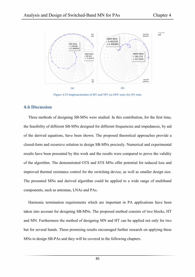
Analysis and Design of Switched-Band MN for PAs Chapter 4
85
(a) (b)
Figure 4.33-Implementation of HT and MN (a) OFF state (b) ON state
4.6 Discussion
Three methods of designing SB-MNs were studied. In this contribution, for the first time,
the feasibility of different SB-MNs designed for different frequencies and impedances, by aid
of the derived equations, have been shown. The proposed theoretical approaches provide a
closed-form and recursive solution to design SB-MNs precisely. Numerical and experimental
results have been presented by this work and the results were compared to prove the validity
of the algorithm. The demonstrated OTS and STS MNs offer potential for reduced loss and
improved thermal resistance control for the switching device, as well as smaller design size.
The presented MNs and derived algorithm could be applied to a wide range of multiband
components, such as antennas, LNAs and PAs.
Harmonic termination requirements which are important in PA applications have been
taken into account for designing SB-MNs. The proposed method consists of two blocks, HT
and MN. Furthermore the method of designing MN and HT can be applied not only for two
but for several bands. These promising results encouraged further research on applying these
MNs to design SB-PAs and they will be covered in the following chapters.
0 1.0
1.0
-1.0
10.0
10.0
-10.0
5.0
5.0
-5.0
2.0
2.0
-2.0
3.0
3.0
-3.0
4.0
4.0
-4.0
0.2
0.2
-0.2
0.4
0.4
-0.4
0.6
0.6
-0.6
0.8
0.8
-0.8
HT2Swp Max
1800MHz
Swp Min
900MHz
900 MHzr 1.05338x 0.496655
1800 MHzr 68.343x -3.16474
S(1,1)
HT2
0 1.0
1.0
-1.0
10.0
10.0
-10.0
5.0
5.0
-5.0
2.0
2.0
-2.0
3.0
3.0
-3.0
4.0
4.0
-4.0
0.2
0.2
-0.2
0.4
0.4
-0.4
0.6
0.6
-0.6
0.8
0.8
-0.8
HTSwp Max
3600MHz
Swp Min
1800MHz
3600 MHzr 156.215x 23.1533
1800 MHzr 0.491525x 0.355882
S(1,1)
HT

86
Chapter 5
Design and Simulation of Dual-Band Class-E Power Amplifiers
Improving a PA’s efficiency is a big concern for PA designers. Switched-mode PAs
theoretically can provide high efficiency as explained in Chapter 2. The conventional
switched-mode PAs (such as Class-E) are performing with high efficiency in narrow and
single bands. Future wireless communication systems, LTE and LTE advanced, will require
PAs to cover more bands of operation with high output power and efficiency. Designing
dual-band PAs with high output power and efficiency is a challenge for PA designers.
The proposed technique in this chapter describes the design of high efficiency Class-E
PAs for single-band and dual-band purposes. The PAs in this work are designed for LTE
communication system. Two bands of LTE standard will cover, 777-787 MHz and 1710-
1785 MHz. In the first section, the method of designing high efficiency Class-E PA is
presented and two single-band PAs are designed to prove the validity of the proposed
technique. In the second and third sections, the same method has been applied to design dual-
band Class-E PAs with two different devices. These PAs are showing high output
performances in terms of both output power and efficiency.
5.1 Single-band Class-E Power Amplifier
The proposed technique is applied to design single-band Class-E PAs in two working
bands. These two PAs are proving the validity of the technique and also, to provide a
reference design to be able to compare performances in single-band and multiband
applications. This method is focusing on providing the required reflection coefficient at the

Design and Simulation of Dual-Band Class-E Power Amplifiers Chapter 5
87
drain of the transistor. This discovery is a key point of this work as it simplifies the Output
Matching Network (OMN) for multiband purposes.
5.1.1 Theory
In this topology, the transistor is assumed to behave as an ideal switch and a nonlinear
capacitor ( dsC ) as shown in Fig. 5.1. Also, the OMN is considered as two parts, the shunt
capacitor ( SC ) and distributed output matching network (DOMN). The DOMN is intended to
provide the required reflection coefficient at the drain of the transistor.
DOMN
Switc
h
Ideal part of transistor
Non-ideal part of
transistor
SCdsC
Figure 5.1-Topology of the design
To find out the desired reflection coefficient, the components of the conventional Class-E
PA’s OMN need to be calculated. The optimum parameters of the lumped element OMN can
be calculated from equations (5.1) to (5.4) which are taken from [16], (load resistance R ,
shunt capacitance C , series capacitance and inductance, 0C and 0L respectively).
2
2 402444.0451759.015768.0L
QQPVR
Lout
DL
(5.1)
2
03175.191424.0144668.5
1
LLLS QQR
C
(5.2)
7879.1101468.11
104823.011
0LLL QQR
C
(5.3)

Design and Simulation of Dual-Band Class-E Power Amplifiers Chapter 5
88
LLRQL 0 (5.4)
These component values are calculated based on specific supply voltage DV , required
output power outP and loaded quality factor ( LQ ). These equations were explained earlier in
more details in Chapter 2.
The DOMN is required to provide the same reflection coefficient as Fig. 5.2 (a); therefore,
LR , 0C and 0L are considered to find its reflection coefficient. Then, the required impedance
at the drain will be found:
)1( 00
LC
jRZ L
(5.5)
PORT1 PORT2
0C 0L
LR PORT2PORT1
(a) (b)
Figure 5.2-OMN (a) basic OMN for Class-E (b) distributed OMN
Transmission lines are preferred to design OMN at microwave frequency as their practical
implementation is more convenient and they give a lower insertion loss, [24] and [18]. In this
method, a single transmission line and a single stub have been used to provide the same
impedance as the conventional lumped OMN, Fig 5.2. Conventional distributed OMN for
Class-E is designed by replacing each lumped component with equivalent transmission line
or stub.
The required shunt capacitor ( sC ) will be added later to the designed OMN. It has been
shown that second harmonic termination (HT) is sufficient to have Class-E performance to a

Design and Simulation of Dual-Band Class-E Power Amplifiers Chapter 5
89
reasonable approximation [97]. Second HT is designed to behave as open circuit at the drain
of the transistor at both frequencies. The design principle of HT is explained in Chapter 4.5.
The second HT circuit and OMN are implemented together to satisfy Class-E requirement.
5.1.2 Simulation of Single-Band Power Amplifiers
Investigation of the validity of the proposed technique is to be proven by designing two
single-band Class-E PAs at two frequency bands, 777-787 MHz and 1710-1785 MHz, which
is suitable for LTE standard. Before starting to simulate PAs, some initial considerations
needed to be thought about. The first one is to choose the right device based on the required
power, operating frequency and etc. The NPTB00004 GaN (Gallium Nitride) HEMT (high
electron mobility transistor) from Nitronex has been chosen. The next step is determining
bias voltage according to the device datasheet and class of operation.
In PA design, there are two MNs, input matching network (IMN) and output matching
network (OMN). The IMN is applied to match the source impedance and the device input
impedance and minimize required input power level to obtain desired output power. The IMN
has been designed by aid of transmission lines and stubs to achieve a reasonably good match.
In this work, the concentration is on OMN to provide high efficiency. The OMN needs to be
designed based on the design equation for Class-E operation. As mentioned earlier, one
transmission line and one stub are replacing the lumped element OMN and provide the same
reflection coefficient. The reflection coefficient of OMN at the drain is sufficient to avoid
overlapping between voltage and current, resulting in a highly efficient PA. The lumped
element components have been calculated based on equation (5.1) to (5.4). These values are
shown in Table 5.1.
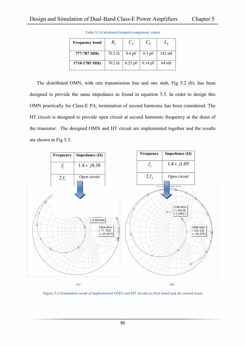
Design and Simulation of Dual-Band Class-E Power Amplifiers Chapter 5
90
Table 5.1-Calculated lumped component values
Frequency band LR SC 0C 0L
777-787 MHz 70.2 Ω 0.6 pF 0.3 pF 142 nH
1710-1785 MHz 70.2 Ω 0.25 pF 0.14 pF 64 nH
The distributed OMN, with one transmission line and one stub, Fig 5.2 (b), has been
designed to provide the same impedance as found in equation 5.5. In order to design this
OMN practically for Class-E PA, termination of second harmonic has been considered. The
HT circuit is designed to provide open circuit at second harmonic frequency at the drain of
the transistor. The designed OMN and HT circuit are implemented together and the results
are shown in Fig 5.3.
Frequency Impedance (Ω)
1f 38.04.1 j
12 f Open circuit
(a) (b)
Figure 5.3-Simulation result of implemented OMN and HT circuit (a) first band and (b) second band
0 1.0
1.0
-1.0
10.0
10.0
-10.0
5.0
5.0
-5.0
2.0
2.0
-2.0
3.0
3.0
-3.0
4.0
4.0
-4.0
0.2
0.2
-0.2
0.4
0.4
-0.4
0.6
0.6
-0.6
0.8
0.8
-0.8
Practical OMNSwp Max
1600MHz
Swp Min
700MHz
d1
782 MHzr 1.40644x 0.381649
1564 MHzr 77.7552x -10.5071
S(1,1)
Practical OMN
d1: Graphs_Auto
0 1.0
1.0
-1.0
10.0
10.0
-10.0
5.0
5.0
-5.0
2.0
2.0
-2.0
3.0
3.0
-3.0
4.0
4.0
-4.0
0.2
0.2
-0.2
0.4
0.4
-0.4
0.6
0.6
-0.6
0.8
0.8
-0.8
OMN and HTSwp Max
4000MHz
Swp Min
1500MHz
1748 MHzr 1.44126x 1.05017
3496 MHzr 152.135x -34.2751
S(1,1)OMN and HT
Frequency Impedance (Ω)
2f 05.14.1 j
22 f Open circuit

Design and Simulation of Dual-Band Class-E Power Amplifiers Chapter 5
91
In Fig 5.3, the required impedances at the fundamental frequencies and the harmonic
frequencies are revealed and the simulated results in the Smith chart shows the perfect match.
This PA has been designed with VVDS 8 and VVGS 5.2 . Table 5.2 and Fig 5.4 are
illustrating the overall performances of these two single-band PAs at two different bands.
Table 5.2- Output performances of the single-band Class-E PAs
Frequency Band Output Power Drain Efficiency PAE
777-787 MHz 35.2 dBm 87.8 % 82.7 %
1710-1785 MHz 36 dBm 85.1% 80.4 %
(a)
(b)
Figure 5.4-Output power and efficincy of the single-band PAs over the whole band of operation (a) first PA and (b)
second PA
0
20
40
60
80
100
0
5
10
15
20
25
30
35
777 778 779 780 781 782 783 784 785 786 787Ef
fici
en
cy (
%)
Ou
tpu
t P
ow
er
(dB
m)
Frequency (MHz)
0102030405060708090100
0
5
10
15
20
25
30
35
17
10
17
15
17
20
17
25
17
30
17
35
17
40
17
45
17
50
17
55
17
60
17
65
17
70
17
75
17
80
17
85
Effi
cie
ncy
(%
)
Ou
tpu
t P
ow
er
(dB
m)
Frequency (MHz)

Design and Simulation of Dual-Band Class-E Power Amplifiers Chapter 5
92
In designing Class-E PAs, avoiding overlap between the voltage and current waveform on
the device plane is important to minimize the power dissipation in the device and
consequently provide high efficiency and optimum performance. The transistors contain both
intrinsic model and extrinsic model. The intrinsic model is an equivalent circuit model of the
transistor which is dependent on the device, and they are surrounded by a package which can
be shown by the extrinsic model and they are dependent on the environment embedding the
device [98]. Package parasitic have a significant effect on the transistor behaviour at
microwave frequency. Therefore, these effects need to be taken into account to make sure the
PA is operating in the intended class of operation. To observe the waveform at the device
plane, a model for the package is required, so that it can be de-embedded [99]. A linear
packaged model for NPTB00004 GaN is introduced in this work. The model of the package
is composed of two inductors and one capacitor. Each physical component is modelled by an
electrical lumped element. The lead-frame and bond wire are the physical components which
are taken into account in this model. The lead-frame of the package is modelled by capacitor
( LC ) and inductor ( LL ), as shown in Fig. 5.5. The bond wire is modelled by an inductor and
its value can be calculated by [115]:
1
)()(4)(1008.5)( 3
mildmillLmillnHL n (5.6)
where l is the length and d is the diameter of the bond wire. The inductance of bond wire
has been calculated 0.4nH as mml 69.1 and mmd 0254.0 , four of them in parallel. The
capacitance of 0.45 pF and inductance of 1.12nH are taken from the package datasheet for
LC and LL , respectively. DSC is an intrinsic and nonlinear capacitance of the device, as shown
in Fig 5.5 [20]. This capacitance has not been taken into account in design of the package
model as its effect needs to be considered to satisfy the required shunt capacitpr.

Design and Simulation of Dual-Band Class-E Power Amplifiers Chapter 5
93
bondwireL LL
LC
Package Model
DSC
Device Plane Package Plane
Figure 5.5-The Package model
To access the waveform at the device plane, the effect of the package element needs to be
cancelled. Another network needs to be introduced which is mirrored version of the package
model with negative values and here this network is called NEGATE. By presenting the
NEGATE network at the drain of the extrinsic transistor, the elements of the package will be
cancelled. Therefore, the waveform at port 2 of the NEGATE network is the waveform at the
device plane, Fig. 5.6. The package model needs to be added after the NEGATE network in
cascade. The cascaded NEGATE and package model provide transparent structure.
Therefore, the obtained waveforms at port 3 are the waveforms at the package plane.
NEGATE Package Model
Device Plane
Intrinsic + Extrinsic Transistor
Package Plane
Figure 5.6-De-embedding package of the transistor with mirrored negative the package model
1 2 3

Design and Simulation of Dual-Band Class-E Power Amplifiers Chapter 5
94
The voltage and current waveforms for both PAs are shown in Fig. 5.7 and 5.8. For both
PAs, the waveforms are illustrated at the device plane and the package plane. The desired
voltage and current waveforms for Class-E mode are observed at the device plane.
(a) (b)
Figure 5.7-Simulated voltage and current waveform for the first PA at (a) the device plane and (b) package plane
(a) (b)
Figure 5.8-Simulated voltage and current waveform for the second PA at (a) the device plane and (b) package plane
When the single-band Class-E PAs have been completed as reference designs and
achieved good performances, it is time to move forward and design dual-band Class-E PA.
5.2 Dual-band Class-E Power Amplifier with GaAs HFET
The actual realisation of dual-band Class-E PA is presented here. Class-E PA has highly
frequency dependent characteristics. Therefore, designing a dual-band Class-E PA is
challenging because optimum output matching and harmonic elimination have to be achieved
0 1 2 2.574
Time (ns)
Waveform
-2
3
8
13
18
2324
-100
36.2
172
308
445
581608
p2
Itime(MODhnnptb00004.X1@2,1)[1,23] (R, mA)PA
Vtime(MODhnnptb00004.X1@2,1)[1,23] (L, V)PA
p1: Freq = 777 MHzPwr = 22 dBm
p2: Freq = 777 MHzPwr = 22 dBm
0 1 2 2.558
Time (ns)
Waveform Deembed
-5
0
5
10
15
20
22
-200
-63
74.1
211
348
485
540
p2
p1
Itime(SUBCKT.S10@2,1)[1,23] (R, mA)PA
Vtime(SUBCKT.S10@2,1)[1,23] (L, V)PA
p1: Freq = 782 MHzPwr = 22 dBm
p2: Freq = 782 MHzPwr = 22 dBm
0 0.4 0.8 1.144
Time (ns)
Waveform
-6
-1
4
9
14
1920
-200
-26.9
146
319
492
665700
p2
Itime(MODhnnptb00004.X1@2,1)[1,23] (R, mA)PA
Vtime(MODhnnptb00004.X1@2,1)[1,23] (L, V)PA
p1: Freq = 1748 MHzPwr = 22 dBm
p2: Freq = 1748 MHzPwr = 22 dBm
0 0.4 0.8 1.144
Time (ns)
Waveform
-1
4
9
14
19
23
-160
-26.7
107
240
373
480
p2
p1
Itime(SUBCKT.S10@2,1)[1,23] (R, mA)PA
Vtime(SUBCKT.S10@2,1)[1,23] (L, V)PA
p1: Freq = 1748 MHzPwr = 22 dBm
p2: Freq = 1748 MHzPwr = 22 dBm
)(VVDS )(VVDS )(mAIDS
)(mAIDS )(VVDS
)(VVDS )(VVDS )(mAIDS )(mAIDS
Design and Simulation of Dual-Band Class-E Power Amplifiers Chapter 5
95
in both bands at the same time with a single OMN to satisfy the required efficiency and
output power in both operating bands. In Chapter 3, some of the MB-PAs and SB-PAs in the
literature, designed with multiband and switched-band MNs, respectively, are discussed.
Here, a quick review of the reported dual-band MNs is presented. Impedance transformers
are a popular technique to design MB-MNs. Two one-sixth-wave transmission line sections
have been proposed with an approximate analytical solution in [100] to provide matching at
0f and its doubled frequency ( 02 f ). Monzon [102] derived an exact analytical solution for
this MN in 2002. Monzon [103] and Orfanidis [104] extended this MN to operate in any two
frequencies (not harmonically related frequencies) in 2003. Designed dual-band MNs in
[100] and [102]-[104] are just able to match resistive loads. Impedance transformers for
complex loads at two frequencies are introduced in [101], [105]-[108]. The obtained
characteristic impedance of transmission lines in [101] and [107] are high and resulting in
very thin transmission lines (which is not practical). Two-section shunt stub transformers are
designed in [108] and provide dual-band matching. The other technique of designing dual-
band MN is presented in [109]. This dual-band MN used a LC multi-resonant circuit to
provide open or short circuit at different frequencies. These MNs suffer from complexity in
design and limitation in the coverage region.
The proposed dual-band MN in this chapter addresses the complexity of the reported
dual-band MNs and is able to provide matching for any frequencies and impedances. As
mentioned in the introduction of this chapter, it is possible to obtain high output performance
in dual-band operation by providing the required reflection coefficient at the drain of the
device. The dual-band PA is designed without switches to minimize the number of
components and reduce the losses introduced by switches. This proposed technique obtained
high efficiency in both bands by simplifying and increasing flexibility of OMN. The

Design and Simulation of Dual-Band Class-E Power Amplifiers Chapter 5
96
possibility of designing a multiband Class-E PA with acceptable performances is increased
by introducing this technique.
5.2.1 Theory
The dual-band Class-E PA presented in this work is designed with a distributed OMN
based on two lumped element networks. Starting from calculating optimum lumped element;
as it is understandable from the equations (5.1) to (5.4), the OMN’s components of Class-E
PA are varied with frequency. There are two ways to design OMN (i) lumped element and
(ii) distributed OMN. OMN for multiband Class-E PA with lumped element would require
switches to satisfy optimum impedance termination for different working bands. Replacing
each component with the equivalent transmission line or stub could be the distributed OMN
method which still requires switches for required working bands. The Class-E PA design
topology in the previous section proved that the reflection coefficient presented at the drain of
the transistor shaped the current and voltage waveforms, and avoid overlapping between
these two waveforms. A single transmission line and a single stub, tuned by width and length,
have been used in the OMN to provide the same reflection coefficient as the lumped element
networks at desired frequencies, Fig 5.2. Having only a single transmission line and a single
stub will enable working simultaneously in two frequencies and make the design more
compact than substituting each component with their equivalent transmission line. This
technique of OMN design makes the circuit more compact and gives a more reliable
performance at both bands of operation. The key point of this PA lies with the ability to
simplify the circuit to enable the achieving of the required Class-E waveform and constant
high efficiency in all bands covered.
The IMN can be designed to be broadband, tunable or dual-band. A broadband IMN
degrades the performance of the PA over the large bandwidth and tunable IMN will introduce

Design and Simulation of Dual-Band Class-E Power Amplifiers Chapter 5
97
losses by using a switch in the network. Therefore, the dual-band IMN is designed to have
promising return loss in both of the desired bands.
5.2.2 Simulation
This dual-band PA is designed for the LTE system to cover two bands, 777-787 MHz and
1710-1785 MHz and output power of 23dBm in both bands. Gallium Arsenide Hetero
junction Field-Effect Transistor (GaAs HFET) is chosen for this dual-band Class-E PA.
Components are calculated for both bands, based on the desired output power and supply
voltage; and LQ set as 10.
The impedance of this lumped element network has been found by aid of equation (5.5).
The OMN with one transmission line and one stub, Fig. 5.2(b), has been designed to provide
the same impedances as found from equation (5.5) at both bands. This dual-band PA
designed without shunt capacitor and assumed internal capacitance of the transistor can fulfil
the required capacitance. In order to design this OMN practically, termination of the second
harmonic frequencies is considered.
5.2.3 Measurement
After completing the CAD design, the PA is ready for physical implementation. The
manufactured PA is shown in Fig. 5.9. This PA has been fabricated with microstrip using a
substrate from Taconic, RF_35_0300 and its properties are shown in Table 5.3. GaAs HFET
from Tri-Quint is used as the power device. In class-E operation, the transistor should be
biased close to pinch off and driven into compression. A few measurements are required to
find the desired gate voltages and RF input power. The pinch off value was obtained from the
device datasheet which is -2.1 V. Then, the PA was driven with different input RF power
levels to find the required input power to make the performance of the PA independent of the
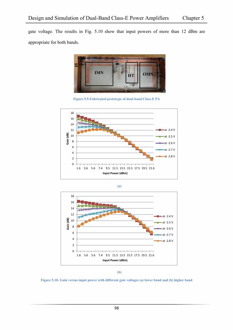
Design and Simulation of Dual-Band Class-E Power Amplifiers Chapter 5
98
gate voltage. The results in Fig. 5.10 show that input powers of more than 12 dBm are
appropriate for both bands.
Figure 5.9-Fabricated prototype of dual-band Class-E PA
(a)
(b)
Figure 5.10- Gain versus input power with different gate voltages (a) lower band and (b) higher band
0
2
4
6
8
10
12
14
16
18
1.6 3.6 5.6 7.4 9.5 11.5 13.5 15.5 17.5 19.5 21.6
Gai
n (
dB
)
Input Power (dBm)
at -2.4 V
at -2.5 V
at -2.6 V
at -2.7 V
at -2.8 V
0
2
4
6
8
10
12
14
16
18
1.6 3.6 5.6 7.4 9.5 11.5 13.5 15.5 17.5 19.5 21.6
Gai
n (
dB
)
Input Power (dBm)
at -2.4 V
at -2.5 V
at -2.6 V
at -2.7 V
at -2.8 V
IMN HT OMN
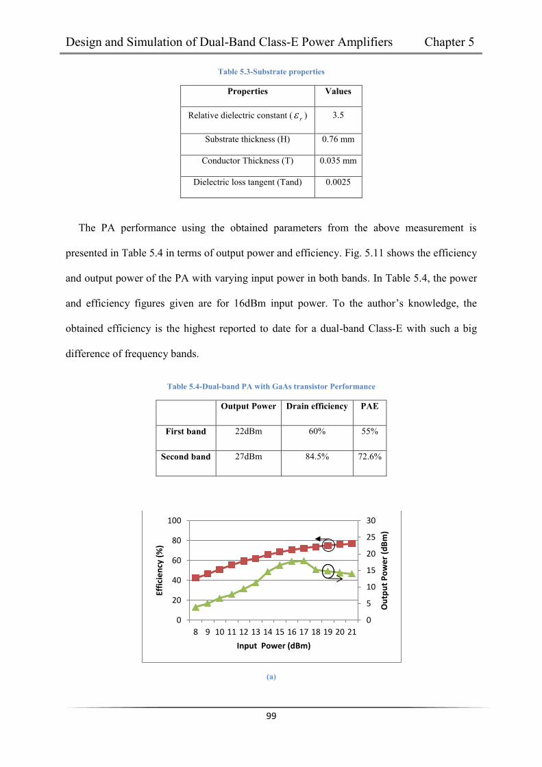
Design and Simulation of Dual-Band Class-E Power Amplifiers Chapter 5
99
Table 5.3-Substrate properties
Properties Values
Relative dielectric constant ( r ) 3.5
Substrate thickness (H) 0.76 mm
Conductor Thickness (T) 0.035 mm
Dielectric loss tangent (Tand) 0.0025
The PA performance using the obtained parameters from the above measurement is
presented in Table 5.4 in terms of output power and efficiency. Fig. 5.11 shows the efficiency
and output power of the PA with varying input power in both bands. In Table 5.4, the power
and efficiency figures given are for 16dBm input power. To the author’s knowledge, the
obtained efficiency is the highest reported to date for a dual-band Class-E with such a big
difference of frequency bands.
Table 5.4-Dual-band PA with GaAs transistor Performance
Output Power Drain efficiency PAE
First band 22dBm 60% 55%
Second band 27dBm 84.5% 72.6%
(a)
0
5
10
15
20
25
30
0
20
40
60
80
100
8 9 10 11 12 13 14 15 16 17 18 19 20 21
Ou
tpu
t P
ow
er
(dB
m)
Effi
cie
ncy
(%
)
Input Power (dBm)
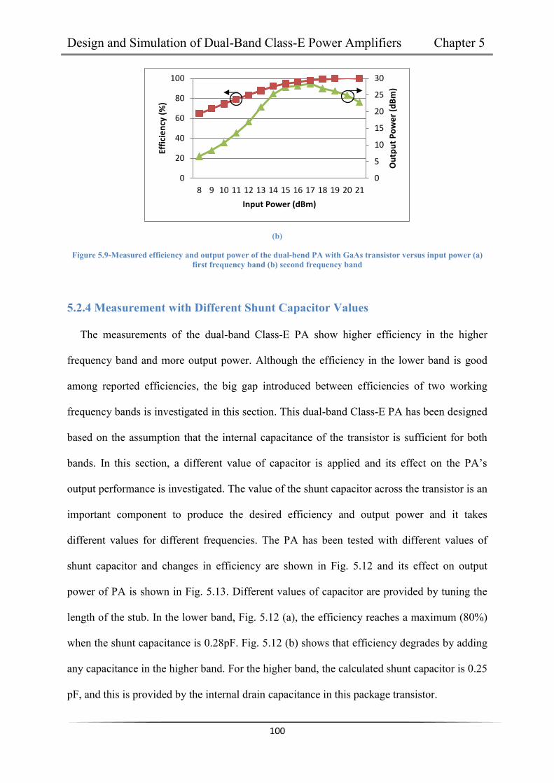
Design and Simulation of Dual-Band Class-E Power Amplifiers Chapter 5
100
(b)
Figure 5.9-Measured efficiency and output power of the dual-bend PA with GaAs transistor versus input power (a) first frequency band (b) second frequency band
5.2.4 Measurement with Different Shunt Capacitor Values
The measurements of the dual-band Class-E PA show higher efficiency in the higher
frequency band and more output power. Although the efficiency in the lower band is good
among reported efficiencies, the big gap introduced between efficiencies of two working
frequency bands is investigated in this section. This dual-band Class-E PA has been designed
based on the assumption that the internal capacitance of the transistor is sufficient for both
bands. In this section, a different value of capacitor is applied and its effect on the PA’s
output performance is investigated. The value of the shunt capacitor across the transistor is an
important component to produce the desired efficiency and output power and it takes
different values for different frequencies. The PA has been tested with different values of
shunt capacitor and changes in efficiency are shown in Fig. 5.12 and its effect on output
power of PA is shown in Fig. 5.13. Different values of capacitor are provided by tuning the
length of the stub. In the lower band, Fig. 5.12 (a), the efficiency reaches a maximum (80%)
when the shunt capacitance is 0.28pF. Fig. 5.12 (b) shows that efficiency degrades by adding
any capacitance in the higher band. For the higher band, the calculated shunt capacitor is 0.25
pF, and this is provided by the internal drain capacitance in this package transistor.
0
5
10
15
20
25
30
0
20
40
60
80
100
8 9 10 11 12 13 14 15 16 17 18 19 20 21
Ou
tpu
t P
ow
er
(dB
m)
Effi
cie
ncy
(%
)
Input Power (dBm)

Design and Simulation of Dual-Band Class-E Power Amplifiers Chapter 5
101
(a)
(b)
Figure 5.10-Efficiency with different shunt capacitor in (a) lower frequency band and (b) higher frequency band. Legend shows the shunt capacitor values
Setting the value of the capacitance close to the ideal value for one of the operating
frequencies using a shunt capacitor will yield a higher performance in that particular band
and relatively lower performance in the other band. One option could be using a capacitance
in between which would degrade the performance of both bands from their ideal result. For
example, 0.14pF could be a suitable compromise capacitance value in between of the
required capacitance of both bands. The resulting efficiencies in the lower and the higher
bands are 65% and 75%, respectively. The efficiency of the lower band increases by 5%,
whereas efficiency of the higher band degrades about 10%. Therefore, to have high efficiency
0
10
20
30
40
50
60
70
80
90
100
7.4 9.4 11.4 13.4 15.4 17.4 19.4
Effi
cie
ncy
(%
)
Input power (dBm)
0 pF
0.07 pF
0.14 pF
0.21 pF
0.28 pF
0.35 pF
0
10
20
30
40
50
60
70
80
90
100
8 10 12 14 16 18 20
Effi
cie
ncy
(%
)
Input Power (dBm)
0 pF
0.07 pF
0.14 pF
0.21 pF
0.28 pF
0.35 pF

Design and Simulation of Dual-Band Class-E Power Amplifiers Chapter 5
102
in both bands, it is required to have different shunt capacitance which could be selected by
using a switch.
(a)
(b)
Figure 5.11-Output Power with different shunt capacitor in (a) lower band and (b) higher band. Legend shows the shunt capacitor values
5.3 Dual-band Class-E Power Amplifier with GaN HEMT
The dual-band Class-E PA with high power transistor, GaN HEMT from Nitronex, has
been designed based on the developed theory to prove the validation of the method. The
similar performances are expected, but with higher output power, as a high power transistor
has been used for this design.
0
5
10
15
20
25
30
35
7.4 9.5 11.5 13.5 15.5 17.5 19.5
Ou
tpu
t P
ow
er
(dB
m)
Input Power (dBm)
0pF
0.07 pF
0.14 pF
0.21 pF
0.28 pF
0.35 pF
0
5
10
15
20
25
30
35
7.4 9.4 11.4 13.4 15.4 17.4 19.4
Ou
tpu
t P
ow
er
(dB
m)
Input Power (dBm)
0pF
0.07 pF
0.14 pF
0.21 pF
0.28 pF
0.35 pF

Design and Simulation of Dual-Band Class-E Power Amplifiers Chapter 5
103
5.3.1 Simulation
The calculated values for optimum OMN are represented in Table 5.1. The OMN has
been designed as explained earlier based on the calculated impedances (equation (5.5)). At
the first stage of the design, the required external shunt capacitor has been ignored and it has
been assumed that the internal capacitance of the device can satisfy the required capacitance.
The simulation result of this PA in both bands is shown in Table 5.5. Output power and
efficiency over the whole band of operation are shown in Fig 5.13. The efficiency and output
power are staying constant over the whole band. Fig. 5.14 shows the voltage (red) and current
(blue) waveform at the device plane in both bands. It is good to note that the waveform of the
second band, Fig. 5.14 (b), provides better coverage and resulting higher output
performances.
Table 5.5-Dual-band Class-E PA with GaN performances
Output Power Drain Efficiency PAE
First band 34.2 dBm 67.6% 61.4%
Second band 35.8 dBm 81.3% 76.8%
(a)
0
20
40
60
80
100
0
5
10
15
20
25
30
35
777 778 779 780 781 782 783 784 785 786 787
Effi
cin
cy (
%)
Ou
tpu
t P
ow
er
(dB
m)
Frequency (MHz)

Design and Simulation of Dual-Band Class-E Power Amplifiers Chapter 5
104
(b)
Figure 5.12-Simulated output power and efficiency of the dual-band PA with GaN transistor over frequency in (a)
lower and (b) higher band
(a) (b)
Figure 5.13-Voltage and current waveforms in (a) lower and (b) higher band
The two different efficiencies in two bands result from the simulated dual-band PA as
explained in the previous section. The higher band provides higher output power and
efficiency, 35.8 dBm and 81.3%. Therefore, it can be concluded that the internal capacitance
of the transistor is satisfying the calculated shunt capacitance (0.25 pF). Lower efficiency and
output power have been obtained in the lower band of operation. The calculated shunt
capacitor for the first band is 0.6 pF and to satisfy this required capacitance, an external shunt
capacitor is needed.
0
20
40
60
80
100
0
5
10
15
20
25
30
35
17
10
17
15
17
20
17
25
17
30
17
35
17
40
17
45
17
50
17
55
17
60
17
65
17
70
17
75
17
80
17
85
Effi
cin
cy (
%)
Ou
tpu
t P
ow
er
(dB
m)
Frequency (MHz)
0 1 2 2.558
Time (ns)
Waveform
-2
3
8
13
18
23
26
-220
-64.6
90.7
246
401
557
650
p2
Itime(MODhnnptb00004.X1@2,1)[1,24] (R, mA)PA
Vtime(MODhnnptb00004.X1@2,1)[1,24] (L, V)PA
p1: Freq = 782 MHzPwr = 23 dBm
p2: Freq = 782 MHzPwr = 23 dBm
0 0.4 0.8 1.144
Time (ns)
Waveform
-6
-1
4
9
14
19
24
28
-220
-25.88
168.2
362.4
556.5
750.6
944.7
1100
p2
Itime(MODhnnptb00004.X1@2,1)[1,24] (R, mA)PA
Vtime(MODhnnptb00004.X1@2,1)[1,24] (L, V)PA
p1: Freq = 1748 MHzPwr = 23 dBm
p2: Freq = 1748 MHzPwr = 23 dBm
][VVDS ][VVDS ][mAIDS ][mAIDS
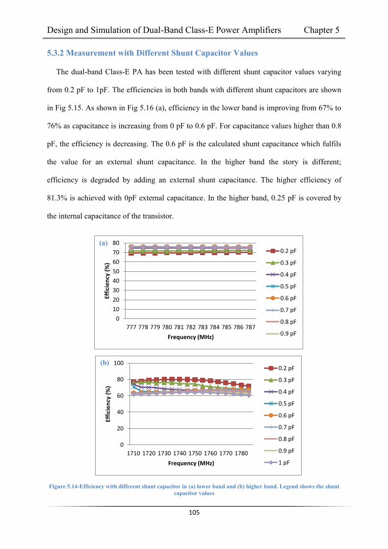
Design and Simulation of Dual-Band Class-E Power Amplifiers Chapter 5
105
5.3.2 Measurement with Different Shunt Capacitor Values
The dual-band Class-E PA has been tested with different shunt capacitor values varying
from 0.2 pF to 1pF. The efficiencies in both bands with different shunt capacitors are shown
in Fig 5.15. As shown in Fig 5.16 (a), efficiency in the lower band is improving from 67% to
76% as capacitance is increasing from 0 pF to 0.6 pF. For capacitance values higher than 0.8
pF, the efficiency is decreasing. The 0.6 pF is the calculated shunt capacitance which fulfils
the value for an external shunt capacitance. In the higher band the story is different;
efficiency is degraded by adding an external shunt capacitance. The higher efficiency of
81.3% is achieved with 0pF external capacitance. In the higher band, 0.25 pF is covered by
the internal capacitance of the transistor.
Figure 5.14-Efficiency with different shunt capacitor in (a) lower band and (b) higher band. Legend shows the shunt capacitor values
0
10
20
30
40
50
60
70
80
777 778 779 780 781 782 783 784 785 786 787
Effi
cie
ncy
(%
)
Frequency (MHz)
0.2 pF
0.3 pF
0.4 pF
0.5 pF
0.6 pF
0.7 pF
0.8 pF
0.9 pF
0
20
40
60
80
100
1710 1720 1730 1740 1750 1760 1770 1780
Effi
cie
ncy
(%
)
Frequency (MHz)
0.2 pF
0.3 pF
0.4 pF
0.5 pF
0.6 pF
0.7 pF
0.8 pF
0.9 pF
1 pF
(b)
(a)

Design and Simulation of Dual-Band Class-E Power Amplifiers Chapter 5
106
5.4 Discussion
This chapter was focused on designing dual-band Class-E PA, starting with two reference
PA design in both desired bands. Two dual-band PAs have been designed with the same
technique but different transistors. Drain efficiency of 60% and 84.5% and output power of
22dBm and 27dBm have been measured for lower band and higher band of operation,
respectively. The second dual-band Class-E PA has been designed with a GaN HEMT. 67%
efficiency and 34.2dBm is the output performance for the lower band of operation, while the
higher band shows 81.3% efficiency and 35.8dBm output power. This design exercise has
demonstrated that having a dual-band Class-E PA in two different and widely separated
bands is feasible at the cost of having a lower efficiency in one of the bands. The different
output performances in the two bands of operation are due to different required shunt
capacitance value across the transistor. Simulations and measurements in the previous section
prove that applying the required external capacitance will improve the PA’s performance at
that specific band. Therefore, a new methodology is proposed in the next chapter to provide
similar and high performances at both bands of operation.
107
Chapter 6
Design and Simulation of Switched-Band Class-E Power Amplifiers
The dual-band Class-E PAs, introduced in the previous chapter, proved the feasibility of
achieving high efficiency in two bands with the proposed technique. There was one
drawback, where higher efficiency was obtained in one band and relatively lower in the other
band. These differences in efficiency have been investigated and are due to the different
required shunt capacitance for two individual frequency bands. In Chapter 5, one solution has
been proposed to achieve the same performance in terms of output power and efficiency in all
working bands by switching the shunt capacitance between the values, depending upon which
band is required.
This chapter will describe the design procedure for switched-band Class-E PAs. The key
point of designing the switched-band Class-E PA in this chapter lies in providing optimum
OMN condition and shunt capacitance by aid of switches to achieve high and constant output
performances in all working bands. Initially, a switched-band Class-E PA with a switch in
OMN and a switched shunt capacitor across the transistor was designed and measured over
two bands of operation. However, the measured result of this PA was not satisfactory in
terms of efficiency in both working bands, compared to the dual-band PA. Therefore, another
switched-band Class-E PA was designed using a switched shunt capacitor and a fixed dual-
band OMN. A fixed dual-band OMN used in conjunction with a switched shunt capacitance
provides similar performances in both bands but with some compromise arising from the
switch losses. A dual-band Class-E PA without a switched shunt capacitance gives better

Design and Simulation of Switched-Band Class-E Power Amplifier Chapter 6
108
performances in one band and worse in the other. The tradeoffs between these design
approaches are examined at the end of the chapter.
6.1 Switchable Matching Power Amplifier
The challenge in this work is to provide high and similar efficiency and output power in
both working bands. A dual-band OMN has been used in the dual-band PA, as explained in
Chapter 5, and obviously, the dual-band OMN is not able to provide the exact required
optimum reflection coefficient for both bands simultaneously. This will reduce the delivered
output power to the load. The proposed switched-band PA in this section has a switch in the
OMN to deliver higher output power to the load and another switch to the shunt capacitor
across the transistor to provide higher efficiency. This PA is called Switchable Matching PA
(SMPA).
6.1.1 Theory
As discussed in Chapter 5, the shunt capacitor is considered as a separate part of OMN in
this Class-E PA design methodology. From now on in this work, the OMN refers to the
matching network, excluding the shunt capacitor. In the SMPA, both OMN and shunt
capacitor are switching to their optimum requirement for each band. The Stub to Short (STS)
OMN is implemented in the SMPA. In Chapter 4, the STS OMN has been explained in more
detail. The STS OMN consists of a transmission line, stub and a switch in the middle of the
stub to switch to ground. The ON state of the switch provides a shorter and grounded stub,
where a longer and open stub is provided by OFF state of the switch. The technique of the
switching in the STS OMN helps to minimize losses which are introduced by the switches, as
explained in Chapter 4. Switching between two optimum OMNs in two different bands
results in delivering more output power to the load because of presenting a better match with
switched-band OMN, rather than the dual-band OMN.

Design and Simulation of Switched-Band Class-E Power Amplifier Chapter 6
109
The presented dual-band PAs in Chapter 5 show that to achieve high efficiency in both
bands of operation, the shunt capacitor across the transistor has to be variable. Therefore, the
shunt capacitor across the transistor needs to switch between two different required
capacitance values. Three methods of switched shunt capacitor are presented here. In the first
method, two stubs are used with a switch in the middle, Fig. 6.1(a). When the switch is OFF,
the stub provides the required capacitance for the higher band of operation (as a shorter stub
is required at higher bands). The length of the ideal stub can be found by:
)..(tan 1101
11 CZcl
(6.1)
where 1C is the required capacitance at the higher band. At the ON state of the switch, the
other stub is introduced into the circuit and provides shunt capacitance at the lower band. The
length of the second stub can be found by (6.1). The other two techniques are using lumped
elements. The first one uses two series capacitors and a switch, Fig. 6.1(b). The OFF state of
the switch provides two series capacitors and the ON state just connects the first capacitor.
1C is the required capacitor at the lower band (switch is ON). The other capacitor should be
optimizing to provide required capacitance by the aid of two series capacitors at the higher
band, and the switch is OFF. The value of the second capacitor can be calculated by
t
t
CCCCC
1
12
. , 1C and tC are the required capacitance for the lower and higher bands,
respectively, and 2C is the series capacitor.
The next technique uses two parallel capacitors with one of the capacitors connected by a
switch to ground, Fig. 6.1(c). When the switch is OFF, the second capacitor is not connected
and required capacitance for the higher band is satisfied by the first capacitor. In the ON state
of the switch, the second capacitor is connected to ground; therefore, the parallel combination
of the capacitors provides the required capacitance for the lower bands. The ON state of the

Design and Simulation of Switched-Band Class-E Power Amplifier Chapter 6
110
switch is applied in the lower band for all of these three methods; on the other hand, the
advantage of method 2 and 3 is switching to ground as this minimises the thermal resistance
which result in providing more reliable operation and reduce the tendency for memory effects
in the non-linear behaviour. Relative performances of these topologies in terms of the amount
of loss are related to the actual loss of component (transmission line and capacitors). RF
current entering to the switches is another factor need to be monitored to analyse the losses of
these topologies.
Tra
nsis
tor
SW
1l
2l
Tra
nsis
tor
1C
2C
SW
1C 2C
SWTra
nsis
tor
(a) (b) (c)
Figure 6.1-Different method of switching capacitors (a) switching between stubs (b) series capacitors (b) parallel capacitors
All of the methods introduced above are feasible if switching between two different
capacitances is required. In some cases (for example this work), only switching to one
capacitor is required as the required capacitance in one of the states is zero. To make this
possible, two switching capacitance methods are presented here. Fig. 6.2(a) illustrates the
Method 1. When the switch is ON, a stub is introduced to the circuit and provides the
required shunt capacitance. The appropriate length for the stub can be calculated by (6.1). In
the OFF state of the switch there is a small residual capacitance which is about 0.007pF.
Method 2 utilizes a capacitor with a switch to the ground, Fig. 6.2(b). The latter method is
preferable as it switches to ground and reduces the losses of the switch.

Design and Simulation of Switched-Band Class-E Power Amplifier Chapter 6
111
Tra
nsis
tor
SW
Tra
nsis
tor
SW
(a) (b)
Figure 6.2- Proposed method for shunt capacitance (a) with a stub (b) with a capacitor
The schematic of the SMPA is shown in Fig. 6.3. In the lower band, 1SW is ON and the
shunt capacitor is connected; whereas, 2SW is OFF and both stubs ( 1S and 2S ) are introduced
into the OMN to present the required reflection coefficient at the drain of the transistor. There
is no need for a shunt capacitor in the higher band as the internal capacitance is sufficient
enough ( 1SW is OFF) but 2SW is ON to present the short stub ( 1S ).
IMNHT
SC
1SW
TL
1S
2S
2SW
Figure 6.3- SMPA schematic
6.1.2 Simulation
The SMPA has been simulated with STS OMN and method 2 of switching the shunt
capacitor. The GaN transistor from Nitronex has been used in the SMPA. The shunt
capacitance of 0.6 pF has been calculated for the lower band of operation and 0.4 pF
capacitance for the higher band, which is satisfied by the internal capacitance of the
transistor. So by turning ON the switch )( 1SW at the lower band and OFF at the higher band,
this requirement is met. As mentioned in the previous section, 2SW (a switch in the OMN) is
OFF in the lower band and ON in the higher band.

Design and Simulation of Switched-Band Class-E Power Amplifier Chapter 6
112
The dual-band IMN (explained in Chapter 5) and HT (explained in Chapter 4) circuit to
terminate the second harmonics have been designed to implement the SMPA. After
completing design of SMPA, the next step is to find required gate voltage bias and
appropriate input power for Class-E operation by sweeping the gate voltage and input power.
The gate voltage of -2.5 V and input power of 22 dBm are desired for this PA. In the lower
band, 34.1 dBm output power and 60% efficiency is achieved. Output power of 33.6 dBm
and efficiency of 71% is reported in the higher band. The NEGATE network is applied to
compensate the effect of the transistor package and observe the waveform at the device plane.
All of the waveforms in this chapter are shown observed at the device plane. The voltage
(pink) and current (blue) waveforms are shown in Fig. 6.4 for the lower and higher band of
operation. As shown in the figure below, there is very small overlap between two waveforms.
This demonstrates that the dissipation power in the transistor is small, which is essential for
high efficiency PA’s performance.
(a) (b)
Figure 6.4-Voltage and current waveform of SMPA in (a) the lower and (b) the higher frequency band
6.1.3 Measurement
Fig. 6.5 shows the photo of the fabricated SMPA. A PIN diode is used as the switch. The
output performance of the SMPA in terms of output power and efficiency is shown in Table
6.1. The simulated and measured output power and efficiency over both lower and higher
0 1 2 2.558
Time (ns)
Waveform OFF Cs
-4
1
6
11
16
21
25
-70
106
282
458
633
809
950
p1
Vtime(MODhnnptb00004.X1@2,1)[1,23] (L, V)PA OFF with Shunt Cap
Itime(MODhnnptb00004.X1@2,1)[1,23] (R, mA)PA ON with Shunt Cap
p1: Freq = 782 MHzPwr = 22 dBm
p2: Freq = 782 MHzPwr = 22 dBm
0 0.4 0.8 1.144
Time (ns)
Waveform ON 3rd HT
-5
0
5
10
15
20
24
-200
-10.3
179
369
559
748
900
p2
Itime(MODhnnptb00004.X1@2,1)[1,23] (R, mA)PA ON with 3rd HT.AP_HB
Vtime(MODhnnptb00004.X1@2,1)[1,23] (L, V)PA ON with 3rd HT
p1: Freq = 1748 MHzPwr = 22 dBm
p2: Freq = 1748 MHzPwr = 22 dBm
][VVDS
][mAIDS
][VVDS
][mAIDS

Design and Simulation of Switched-Band Class-E Power Amplifier Chapter 6
113
frequency bands are shown in Fig. 6.6. Output power of 30.7 dBm and 31.5 dBm for the
lower and the higher band have been measured and show degradation in output power which
is due to practical implementation. It is worth highlighting that the efficiency and output
power maintain almost constant values over the whole bandwidth of both bands.
Table 6.1-SMPA output performances
Output Power Drain Efficiency PAE
Lower band 30.7 dBm 60% 46%
Higher band 31.5 dBm 61% 44%
Figure 6.5-Fabricated prototype of switched-band Class-E PA
As the measurement results reveal efficiency and output power are lower compare to the
reported efficiency of dual-band Class-E PA in Chapter 5. Two switches have been applied in
the OMN of the SMPA and accordingly, two bias networks for PIN diodes. Each of the
lumped components and switches will introduce loss in the network. These losses (especially
switches’ losses) produce heat and dissipate power and have impact on the efficiency. To
overcome this problem, a switched-band Class-E PA needs to design with fewer switches.
6.2 Fixed Matching Power Amplifier
A novel technique to design a switched-band PA was presented in the previous section and
called SMPA. The SMPA showed the similar performances for both bands of operation in
terms of output power and efficiency. However, the reported output performances decreased
OMN IMN SC

Design and Simulation of Switched-Band Class-E Power Amplifier Chapter 6
114
compared to the dual-band Class-E PA, in Chapter 5. Another method of designing switched-
band Class-E PA with fewer switches is presented here. The switch in the OMN will be
eliminated and dual-band OMN will be used instead. The only switch in this design
methodology is the switch for shunt capacitor as its effect on improving the efficiency has
been proved in the previous chapter. This PA is called Fixed Matching PA (FMPA), as there
is no switch in the OMN and just the shunt capacitance is switched.
(a)
(b)
Figure 6.6-Output power and efficiency of simulation and measurement of SMPA in (a) the lower and (b) the higher
band
0
10
20
30
40
50
60
70
80
90
100
0
5
10
15
20
25
30
35
777 778 779 780 781 782 783 784 785 786 787
Effi
cie
ncy
(%
)
Ou
tpu
t P
ow
er
(dB
m)
Frequency (MHz)
Sim Pout
Meas Pout
Sim Eff
Meas Eff
0
10
20
30
40
50
60
70
80
90
100
0
5
10
15
20
25
30
35
17
10
17
15
17
20
17
25
17
30
17
35
17
40
17
45
17
50
17
55
17
60
17
65
17
70
17
75
17
80
17
85
Effi
cie
ncy
(%
)
Ou
tpu
t P
ow
er
(dB
m)
Frequency (MHz)
Sim Pout
Meas Pout
Sim Eff
Meas Eff

Design and Simulation of Switched-Band Class-E Power Amplifier Chapter 6
115
6.2.1 Theory
The FMPA has been designed with the dual-band OMN as described in Chapter 5 by aid
of a transmission line (TL) and a stub (S), shown in Fig.6.7. The only switch in the FMPA is
applied to the shunt capacitance across the transistor, method 2 of switching (Fig.6.2(b)). As
it explained in section 6.1.1, the SW is ON for the lower band and OFF for the higher band of
operation. The advantages of this method are that there are fewer switches, switching to
ground to decrease the losses of the switch and also, that the switch is ON only in the lower
band of operation.
IMNHT
SC
SW
TL
S
Figure 6.7- FMPA schematic
6.2.2 Simulation
The FMPA has been simulated in AWR for LTE application with the same GaN HEMT.
The dual-band OMN has been designed based on the calculated lumped element component.
The calculated shunt capacitance is 0.6 pF for the lower band. A 0.6 pF capacitor and a PIN
diode are applied across the transistor. In the lower band the PIN diode is ON, connecting the
capacitor to the ground, therefore, the shunt capacitor is introduced across the transistor. In
the higher band of operation, the PIN diode is OFF and the capacitor is disconnected. Similar
to the previous PAs, the second HT circuit and dual-band IMN are designed and applied for
this PA. Class-E PA is a switched-mode PA and the transistor operates as a switch (ON and
OFF state), which means that the transistor should be driven into compression by aid of an
appropriate input power and gate voltage bias. The same gate voltage and input power (as

Design and Simulation of Switched-Band Class-E Power Amplifier Chapter 6
116
reported in 6.1.2) are applied for the FMPA. The performance of the FMPA is summarised in
the Table 6.2. The efficiency and output power performances in both band of operation for
ON and OFF state of the switch are presented in Fig 6.9. As shown in Fig.6.9, the efficiency
stays constant for both band and above 70% and the output power is about 34 dBm. The
current and voltage waveforms at the device plane are shown in Fig 6.8. These waveforms
are presenting the acceptable Class-E waveforms condition.
Table 6.2-Dual-band OMN and switched shunt capacitance Class-E PA (FMPA) Performances
Output Power Drain Efficiency PAE
First band 34 dBm 74.8% 67.4%
Second band 35.1 dBm 72.5% 67.2%
(a) (b)
Figure 6.8-Voltage and current waveforms of FMPA in (a) ON and (b) OFF state
0 1 2 2.558
Time (ns)
Waveform Switched CS ON
-1
4
9
14
19
24
28
-200
-34.5
131
297
462
628
760
p2
Itime(MODhnnptb00004.X1@2,1)[1,24] (R, mA)PA with switched Cs ON
Vtime(MODhnnptb00004.X1@2,1)[1,24] (L, V)PA with switched Cs ON
p1: Freq = 782 MHzPwr = 23 dBm
p2: Freq = 782 MHzPwr = 23 dBm
0 0.4 0.8 1.144
Time (ns)
Waveform Switched Cs OFF
0
5
10
15
20
25
27
-100
103.7
307.4
511.1
714.8
918.5
1000
p2
Itime(MODhnnptb00004.X1@2,1)[1,23] (R, mA)PA with switched Cs OFF
Vtime(MODhnnptb00004.X1@2,1)[1,24] (L, V)PA with switched Cs OFF
p1: Freq = 1748 MHzPwr = 22 dBm
p2: Freq = 1748 MHzPwr = 23 dBm
][VVDS
][mAIDS
][VVDS
][mAIDS

Design and Simulation of Switched-Band Class-E Power Amplifier Chapter 6
117
(a)
(b)
Figure 6.9-Output power and efficiency of FMPA over frequency in (a) OFF state and (b) ON state
The simulation result of the FMPA illustrates similar performances in both bands. This PA
has not been fabricated due to lack of time but similar measured performances as the
simulation result are expected as reasonable agreement between simulation and measurement
was achieved in the previous switched-band Class-E PA.
0
20
40
60
80
100
0
5
10
15
20
25
30
35
777 778 779 780 781 782 783 784 785 786 787
Effi
cie
ncy
(%
)
Ou
tpu
t P
ow
er
(dB
m)
Frequency (MHz)
0102030405060708090100
0
5
10
15
20
25
30
35
17
10
17
15
17
20
17
25
17
30
17
35
17
40
17
45
17
50
17
55
17
60
17
65
17
70
17
75
17
80
17
85
Effi
cie
ncy
(%)
Ou
tpu
t P
ow
er
(dB
m)
Frequency (MHz)

Design and Simulation of Switched-Band Class-E Power Amplifier Chapter 6
118
6.3 Discussion
Providing the similar performances in all bands of multiband PAs is a challenge for PA
designers. Two switched-band Class-E PAs have been analyzed in this chapter, SMPA and
FMPA. Table 6.3 summarize performances of the reported switched-band Class-E PAs and
the proposed PAs in this work. Techniques of these PAs ([81], [88]-[89]) are explained in
Chapter 3. As shown in this Table, the proposed switched-band Class-E PAs (SMPA and
FMPA) in this Chapter perform with higher efficiency compared to the existing SB-PAs in
this class of operation.
The SMPA has two switches in the OMN and provides the efficiency of about 60% for the
both bands. Only one switch has been applied in the FMPA to switch the shunt capacitor and
provide efficiency of about 70% for both bands. The FMPA has following advantages:
Only one switch is applied
The switch is ON in the lower band of operation
Similar and high performances in both bands
About 10% improvement in efficiency compared to SMPA
Table 6.3-Switched-band Class-E PAs
References Band of operation
(GHz)
Output Power
(dBm)
Drain Efficiency
(%) PAE (%)
[81] 0.9 and 1.8 20 38 and 26 N.A
[88] 1.9-2.3-2.6-3.5 24.2-23.8-23.4-20.5 48.2-44.3-40.9-35.6 N.A
[89] 1.7 and 2.5 28 and 27 N.A 57 and 61.5
This work
(SMPA) 0.782 and 1.748 34.1 and 33.6 60 and 71 56.3 and 66.1
This work
(FMPA) 0.782 and 1.748 34 and 35.1 74.8 and 72.5 67.4 and 67.2

119
Chapter 7
Conclusion Fast growth in the number of users of the wireless communication systems attracts a lot of
attention from researchers to improve the quality of this service by increasing battery life,
improving reliability, reducing the size and weight, and lowering the cost of the devices,
while providing internet connections for users everywhere and anytime without decreasing
the speed and the quality of service. These requirements can be met by designing high
efficiency and adaptive transmitters. The main concern of the presented research in this thesis
was to study and discover a methodology for designing high efficiency frequency adaptive
PA (the most challenging component of the transmitter) for wireless communication systems.
Achievements during this study were:
Designed SB-MNs and minimised losses of the switch and derived an original
recursive analytical solution for all the proposed MNs.
Developed an approach to the design of Class-E PA with distributed MNs based on
reflection coefficient approach with high efficiency performances.
Proposed design methodology of dual-band Class-E PA with high output
performance, but higher efficiency obtained in the higher band of operation.
Proposed and designed two switched-band Class-E PAs: Switchable Matching PA
(SMPA) and Fixed Matching PA (FMPA), similar and high output performance
was achieved. Both used switched shunt capacitor to maintain Class-E operation in
the selected band.

Conclusion Chapter 7
120
Discussed and compared the feasibility of dual-band and switched-band Class-E
PAs, showing the trade-offs that need to be considered by designers of PAs for
engineering multiband communication standards.
7.1 Thesis Summary
This research started with the background review on the important merits of the PAs and
devices, as shown in Chapter 2. All the reported techniques of designing frequency adaptive
PAs (multiband and switched-band) are discussed in Chapter 3. One approach to design a
PA for multiband systems is designing a broadband PA; low efficiency and limited gain are
drawbacks of this approach. The other approaches are MB-PAs and SB-PAs and Chapter 3 is
mainly concentrated on these two approaches. This research proved that designing with MB-
MN or SB-MN has better performances compare to utilizing parallel single-band PAs (with
or without switches). This literature review on the current techniques clarified the need for
research on discovering a methodology to design frequency adaptive PAs to perform with
high PAE at all the frequency bands.
The design of high efficiency frequency adaptive PAs started with designing SB- MN with
the purpose of reducing losses of the switches in the circuit and providing more accurate
results in all the working bands. Three methods (detach- , short- and open- stub) to design
SB-MN were presented in Chapter 4. The Open to Short stub (OTS) and Short to Stub (STS)
methods are more compact compared with the detach stub [21], [73], [110] and methods
involving switching between two individual MNs [86], [87]. OTS and STS address the
thermal problem of PIN diodes by connecting one terminal to ground. In this contribution, for
the first time, the feasibility of SB-MNs for different frequencies, by aid of the derived
equations, has been shown. The proposed theoretical approach, based on the SB-MNs,
provides a closed-form and recursive solution to design SB-MNs precisely, given any two

Conclusion Chapter 7
121
frequencies. Furthermore these methods can be applied not only for two but for several band
MNs. Numerical and experimental results have been presented by this work and the results
were compared to prove the validity of the algorithm. The presented MNs and derived
algorithm could be applied to a wide range of multiband components, such as antennas,
LNAs and PAs. These promising results encouraged further research on designing SB-MNs
that take account of harmonic termination requirements, which are important in PA
applications. The proposed method consists of two blocks, HT (Harmonic Termination
Network) and MN.
Chapter 5 has presented the design methodology of high efficiency Class-E PA to work
in single-band and multiband application. Dual-band Class-E PAs are presented to operate in
an up-link band of the LTE system. Dual-band OMN is applied to achieve amplification in
both bands without any switches (GaAs HFET has been used in this design) and measured
high drain efficiency of 60% and 84.5% and output power of 22 and 27 dBm at 777-787 and
1718-1785 MHz, respectively. The same technique is applied with another transistor (GaN
HEMT). This dual-band Class-E PA provides dual-band amplification with drain efficiency
of 67.7% and output power of 34.2 dBm at first band and 81.3% drain efficiency and
35.8dBm output power at the second band. Both dual-band Class-E PAs perform with
satisfying high efficiency and provide higher efficiency at the higher band of operation. The
reason for the different efficiencies in the two bands was addressed and is due to the
requirement of different shunt capacitance across the transistor in different operating
frequencies.
The difference in efficiencies at both bands of operation is overcome in Chapter 6 by
applying SB-MNs in the circuit. Two switched-band Class-E PAs were proposed in this
chapter. The first PA, SMPA, utilises a switch for OMN and another switch to change the

Conclusion Chapter 7
122
value of shunt capacitance for both bands. The measurement result of SMPA shows 30.7 and
31.5 dBm output power in the two bands with drain efficiency of 60% and 61%, respectively.
The second SB-PA, FMPA, was designed with dual-band OMN and a switched shunt
capacitor. Output power of 34 and 35.1 dBm and drain efficiency of 74.8% and 72.5%
achieved from this PA at the lower and higher band of operation, respectively. The FMPA
reduced the number of switches in the circuit and improved the efficiency about 10%
compared to SMPA. The similar performances in both bands have been achieved in the SB-
PAs at the cost of decreasing efficiency in the higher band.
7.2 Conclusion
For comparison purposes, performances of all the designed Class-E PA in this work are
shown in the Table 7.1. This table shows the simulated result in each case in order to provide
a consistent comparison. Confidence in the validity of the results has been demonstrated by
building and testing several example designs.
Table 7.1-Simulation performance comparison between all the designed Class-E PAs
Output Power (dBm) Efficiency (%) PAE (%)
Band of Operation 1f 2f 1f 2f 1f 2f
Dual-band PA 34.2 35.8 67.6 81.3 61.4 76.8
SMPA 34.1 33.6 60 71 56.3 66.1
FMPA 34 35.1 74.8 72.5 67.4 67.2
The best obtained efficiency is from the dual-band PA at the second band. Efficiency of
about 70% was obtained for both bands in FMPA. The key factor discovered here was the
need to switch the parallel capacitor value. There is a trade off between providing highest
possible efficiency in one band at the cost of degrading efficiency in the other band (dual-
band PA) or obtaining similar performances for both bands (FMPA). In the dual-band PA and

Conclusion Chapter 7
123
FMPA, there is a limitation to the number of bands that can be covered, whereas SMPA is
capable of covering more bands of frequency by applying more switches, although this
results in introducing more losses.
7.3 Future Work
This thesis has advanced in the research area of high efficiency adaptive PA design. Like
any research, lots of questions and ideas arise during the study, which some of them still
remained unanswered and uncovered. Some of them are presented here as possible research
works. This research was mainly focusing on improving the efficiency of frequency adaptive
PAs. The chosen class of operation in this work (Class-E) is inherently nonlinear because the
active device acts as a switch. Linearity of a PA is one of the important factors. By improving
efficiency of a PA, linearity will normally be reduced and vice versa. Linearity of the
proposed PAs in this work has not been investigated. Future work for the proposed high
efficiency PAs is to linearize them with one of the current techniques; such as, pre-distortion
[13] and Envelope Elimination and Restoration (EER) [111]-[112].
Another future work is to design a PA with ability of switching between broadband and
narrow-band high efficiency PA (switching operation modes of PA). This design can use a
Class-E highly efficient PA to work in a narrow band of frequencies and a Class-B PA to
cover broader bandwidths when required.

124
References 1. B. A. Fette, Cognitive Radio Technology, 2nd edition, Elsevier, 2009.
2. T. S. Rappaport, “Wireless Communication: Principles and Practice”, 2nd Edition,
Prentice Hall, 2001.
3. T. W. Rondeau, and C. W. Bostian, Artificial Intelligence in Wireless Communication,
London: mobile communication series, 2009.
4. S. C. Cripps, RF power amplifiers for wireless communications, 2nd Edition, Artech
House Publishers, 2006.
5. F. H. Raab, P. Asbeck, et al, “Power Amplifiers and Transmitters for RF and
Microwave”, IEEE Transaction on Microwave Theory and Techniques, vol.50, no.3,
March 2002.
6. Y. Chung, C. Y. Hang, S. Cai et al, “AlGAn/GaN HFET Power Amplifier Integrated
With Microstrip Antenna for RF Front-End Applications”, IEEE Transaction on
Microwave Theory and Techniques, vol.51, no.2, pp.653-659, February 2003.
7. N. O. Sokal, N.O. and A. D. Sokal, “Class E-A New Class of High-Efficiency Tuned
Single-Ended Switching Power Amplifiers”, IEEE Journal of Solid-State Circuits, Vol.
SC-10. No. 3, pp.168-176, 1975.
8. F. H. Raab, "Effects of circuit variations on the class E tuned power amplifier," IEEE
Journal of Solid-State Circuits, vol.13, no.2, pp.239-247, April 1978.
9. Y. Qin, S. Gao, A. Sambell, “Broadband High-Efficiency Circularly Polarized Active
Antenna and Array for RF Front-End Application”, IEEE Transactions on Microwave
Theory and Techniques, Vol. 54, No. 7,pp. 2910-2916, 2006.
10. D. P. Kimber, Class E Amplifiers and their Modulation Behaviour, Thesis submitted at
the University of Birmingham, 2005.

References
125
11. F. H. Raab, P. Asbeck, S. Cripps, P. B. Kenington, Z. B. Popovic, N. Pothecary, J. F.
Sevic, N. O. Sokal, “RF and Microwave Power Amplifier and Transmitter Technologies”,
High Frequency Electronics, pp.22-54, May 2003- January 2004.
12. S. C. Cripps, RF Power Amplifiers for Wireless Communications, Norwood: Artech
House, 2008.
13. S. C. Cripps, RF Power Amplifiers for Wireless Communications, Norwood: Artech
House, 1999.
14. G. D. Vendelin, A. M. Pavio, and U. L. Rohde, Microwave Circuit Design Using Linear
and Nonlinear Techniques, 2nd edition, Canada: Wiley Intercience, 2005.
15. P. Wright, J. Lees, J. Benedikt, P. J. Tasker, S. C. Cripps, “A Methodology for Realizing
High Efficiency Class-J in Linear and Broadband PA”, IEEE Transaction on Microwave
Theory and Techniques, vol.57, no.12, pp.3196-3204, December 2009.
16. N. O. Sokal, “Class-E RF Power Amplifiers”, QEX, No. 204, pp.9-20, January/February
2001.
17. T. B. Mader, E. W. Bryerton, M. Markovic, et al “Switched-Mode High-Efficiency
Microwave Power Amplifiers in a Free-Space Power-Combiner Array”, IEEE
Transactions on Microwave Theory and Techniques, Vol. 46, No.10, pp.1391-1398,
1998.
18. A. Grebennikov and N. O. Sokal, Switchmode RF Power Amplifiers, Linacre House,
Jordan Hill, Oxford OX2 8DP, UK, 2007.
19. A. M. Mohamed, S. Boumaiza, R. R. Mansour, “Novel Reconfigurable
Fundamental/Harmonic Matching Network for Enhancing the Efficiency of Power
Amplifiers”, 40th European Microwave Conference, 2010.
20. A. Sheikh, “High Power Waveform Engineering”, PhD Thesis, University of Wales,
Cardiff University, Cardiff, June 2009.

References
126
21. A. Fukuda, H. Okazaki, T. Hirota and Y. Yamao, “Novel 900 MHz/1.9 GHz Dual-
Mode Power Amplifier Employing MEMS Switches for Optimum Matching”, IEEE
Microwave and Wireless Components Letters, vol.14, no.3, pp. 121-123, March 2004.
22. A. Fukuda, T. Furuta, H. Okazaki, S. Narahashi, “A 0.9-5-GHz Wide-Range 1 W-Class
Reconfigurable Power Amplifier Employing RF-MEMS Switches”, IEEE, pp. 1859-
1862, 2006.
23. J. Kim, F. Mkadem, S. Boumaiza, “A High Efficiency and Multi-Band/Multi-Mode
Power Amplifier using a Distributed Second Harmonic Termination”, 40th European
Microwave Conference, pp 1662-1665, 2010.
24. M. Watertown, The PIN Diode Circuit Designers’ Handbook, Massachusetts: Microsemi
Corporation, 1998.
25. G. M. Rebeiz and J. B. Muldavin, “RF MEMS Switches and Switch Circuits”, IEEE
Microwave Magazine, pp. 59-71, 2001.
26. Y. Yashchyshyn, “Reconfigurable Antennas by RF Switches Technology”, MEMSTECH,
pp. 155-157, 2006.
27. Skyworks Solutions Inc, “Application Note: Varactor Diodes”, Skyworks, 2008.
28. W. C. Edmund Neo, Y. Lin, X. D. Liu; L. C. N. De Vreede, L. E. Larson, M. Spirito, M.
J. Pelk, K. Buisman, A. Akhnoukh, A. Anton de Graauw, L. K. Nanver, "Adaptive Multi-
Band Multi-Mode Power Amplifier Using Integrated Varactor-Based Tunable Matching
Networks," IEEE Journal of Solid-State Circuits, vol.41, no.9, pp.2166-2176, September
2006.
29. B. Doherty, and M. Watertown, “PIN Diode Fundamental”, MicroNote series 701.
30. G. Hiller, “Design with PIN Diodes”, Application Notes.

References
127
31. A. C. K. Mak, C. R. Rowell, R. D. Murch, and C. Mak, “Reconfigurable Multiband
Antenna Designs for Wireless Communication Devices”, IEEE Transactions on Antennas
and Propagation, vol. 55, no. 7, pp. 1919-1928, 2007.
32. E. G. Jeckeln, F. M. Ghannouchi, F.M. and M. A. Sawan, “A New Adaptive Predistortion
Technique Using Software-Defined Radio and DSP Technologies Suitable for Base
Station 3G Power Amplifiers”, IEEE Transactions on Microwave Theory and
Techniques, Vol. 52, No. 9, pp.2139-2147, 2004.
33. S. Bruss, “Linearization Methods”, pp.1-8, 2003.
34. J. C. Pedro, N. B. Carvalho, Intermodulation Distortion in Microwave and Wireless
Circuits, Artech House, Norwood, 2003.
35. J. Yi, Y. Yang, M. Park, W. Kang, et al, "Analog predistortion linearizer for high-power
RF amplifiers," IEEE Transactions on Microwave Theory and Techniques, vol.48, no.12,
pp.2709-2713, December 2000.
36. F. H. Raab, P. Asbeck, S. Cripps, et al “RF and Microwave Power Amplifier and
Transmitter Technologies-Part 4”, High Frequency Electronics, pp.38-49, November
2003.
37. M. A. Briffa, Linearization of RF Power Amplifiers, Doctor of Philosophy thesis,
Melbourne 1996.
38. J. H. Chen, K. U-yen, J. S. Kenney, "An envelope elimination and restoration power
amplifier using a CMOS dynamic power supply circuit," IEEE MTT-S
International Microwave Symposium Digest, vol.3, pp.1519-1522, 6-11 June 2004.
39. F. H. Raab, “Idealized Operation of the Class E Tuned Power Amplifier”, IEEE
Transaction on Circuits and Systems, pp.725-735, 1977.
40. D. M. Pozar, Microwave Engineering, University of Massachusetts, 2005.

References
128
41. R. Sorrentino, G. Bianchi, Microwave and RF Engineering, 1st edition, John Wiley &
Sons, 2010.
42. S. C. Cripps, Advanced Technique in RF Power Amplifier Design, Artech House
Publishers, 2002.
43. P. Savary, A. Girardot, G. Montoriol, F. Dupis, B. Thibaud, R. Jaoui, L. Chapoux, V.
Esnault, L. Cornibert, O. Izumi, D. Hill, M. Sadaka, H. Henry, E. Yu, M. Tutt, M.
Mejerus, R. Uscola, F. Clayton, C. Rampley, S. Klingbeil, K. Rajagopalan, A. Mitra, and
A. Reyes, “Dual-band Multi-Mode Power Amplifier Module Using A Third Generation
HBT Technology”, IEEE Gallium Arsenide Integrated Circuit Symp, pp.71-74, 2001.
44. D. Kalim, R. Negra, "Concurrent planar multiharmonic dual-band load coupling network
for switching-mode power amplifiers," IEEE MTT-S International Microwave Symposium
Digest (MTT), pp.1-4, 5-10 June 2011.
45. K. Uchida, Y. Takayama, T. Fujita, K. Maenaka, “Dual-Ban GaAs FET Power Amplifier
with Two-Frequency Matching Circuits”, Asia-Pacific Microwave Conference, vol.1,
2005.
46. S. H. Ji, C. S. Cho, J. W. Lee, J. Kim, “Concurrent Dual-Band Class-E Power Amplifier
Using Composite Right/Left-Handed Transmission Lines”, IEEE Transactions on
Microwave Theory and Techniques, vol. 55, no. 6, pp. 1341-1374, June 2007.
47. J. L. Jimenez-Martin, V. Gonzalez-Posadas, F. J. Arques, L. E. Garcia-Munoz, D.
Secovia-Vargas, “Dual Band High Efficiency Power Amplifier Based on CRLH Lines”,
RADIOENGINEERING, vol.18, no.4, pp.567-578, December 2009.
48. J. Shi, T. Liu, Y. Ye, S. Ge, G. Xu, "Dual-Band Power Amplifier Using Composite
Right/Left-Handed Transmission Line," 6th International Conference on Wireless
Communications Networking and Mobile Computing (WiCOM), pp.1-4, 23-25 September
2010.
References
129
49. A. Fukuda, H. Okazaki, S. Narahashi, T. Nojima, "Concurrent multi-band power
amplifier employing multi-section impedance transformer," IEEE Topical Conference
on Power Amplifiers for Wireless and Radio Applications (PAWR), pp.37-40, 16-19
January 2011.
50. A. Fukuda, H. Okazaki, S. Narahashi, T. Nojima, "A concurrent multi-band power
amplifier with compact matching networks," General Assembly and Scientific
Symposium, pp.1-4, August 2011.
51. A. Fukuda, H. Okazaki, S. Narahashi, "Novel multi-band matching scheme for highly
efficient power amplifier," European Microwave Conference, EuMC, pp.1086-1089,
2009.
52. S. Pei, J. Nan, Y. Qu, "Two kinds of dual-band power amplifier matching networks using
three-section microstrip line," 10th International Symposium on Antennas, Propagation &
EM Theory (ISAPE), pp.702-705, 22-26 October 2012.
53. X. Fu, D. T. Bespalko, S. Boumaiza, "Novel Dual-Band Matching Network for Effective
Design of Concurrent Dual-Band Power Amplifiers," IEEE Transactions on Circuits and
Systems I: Regular Papers, vol.61, no.1, pp.293-301, January 2014.
54. K. Rawat, F. M. Ghannouchi, "Dual-band matching technique based on dual-
characteristic impedance transformers for dual-band power amplifiers
design," Microwaves, Antennas & Propagation, IET , vol.5, no.14, pp.1720-1729,
November 2011.
55. Y. Ding, Y. X. Guo, F. L. Liu, "High-efficiency concurrent dual-band class-F and inverse
class-F power amplifier," Electronics Letters , vol.47, no.15, pp.847-849, July 2011.
56. R. Liu, D. Schreurs, W. De Raedt, F. Vanaverbeke, R. Mertens, "Concurrent dual-band
power amplifier with different operation modes," IEEE MTT-S International Microwave
Symposium Digest (MTT), pp.1-4, 5-10 June 2011.

References
130
57. P. Saad, P. Colantonio, M. Junghwan, L. Piazzon, F. Giannini, K. Andersson, B. Kim, C.
Fager, "Concurrent dual-band GaN-HEMT power amplifier at 1.8 GHz and 2.4
GHz," IEEE 13th Annual Wireless and Microwave Technology Conference (WAMICON),
pp.1-5, 15-17 April 2012.
58. P. Saad, P. Colantonio, L. Piazzon, F. Giannini, K. Andersson, C. Fager, "Design of a
Concurrent Dual-Band 1.8–2.4-GHz GaN-HEMT Doherty Power Amplifier," IEEE
Transactions on Microwave Theory and Techniques, vol.60, no.6, pp.1840-1849, June
2012.
59. K. Rawat, F. M. Ghannouchi, "Design Methodology for Dual-Band Doherty Power
Amplifier With Performance Enhancement Using Dual-Band Offset Lines," IEEE
Transactions on Industrial Electronics, vol.59, no.12, pp.4831-4842, December 2012.
60. A. Cidronali, N. Giovanneli, I. Magrini, G. Manes, “Compact Concurrent Dual-Band
Power Amplifier for 1.9GHz WCDMA and 3.5GHz OFDM Wireless Systems”, 3rd
European Microwave Integrated Circuits Conference, Amsterdam, pp.518-521, 2008.
61. P. Colantonio, F. Giannini, R. Giofre, L. Piazzon, “A Design Technique for Concurrent
Dual-Band Harmonic Tuned Power Amplifier”, IEEE Transactions on Microwave Theory
and Techniques, Vol. 56, No. 11, pp. 2545-2555, 2008.
62. M. R. Ghajar, S. Boumaiza, "Concurrent dual band 2.4/3.5GHz fully integrated power
amplifier in 0.13µm CMOS technology," Microwave Integrated Circuits Conference,
2009. EuMIC 2009. European, pp.375-378, Rome, 28-29 September 2009.
63. D. T. Bespalko and S. Boumaiza, “Concurrent Dual-Band GaN Power Amplifier with
Compact Microstrip Matching Network”, Microwave and Optical technology Letters,
vol.51, no.5, pp.1604-1607, 2009.
64. S. Gao, Z. Wang, C. W. Park, "Concurrent dual-band power amplifier with second
harmonic controlled by gate and drain bias circuit," IEEE International Conference

References
131
on Microwave Technology & Computational Electromagnetics (ICMTCE), pp.309-312,
22-25 May 2011.
65. R. Negra, A, Sadeve, S. Bensmida, F. M. Ghannouchi, "Concurrent Dual-Band Class-F
Load Coupling Network for Applications at 1.7 and 2.14 GHz," IEEE Transactions
on Circuits and Systems II: Express Briefs, vol.55, no.3, pp.259-263, March 2008.
66. R. Zhang, M. Acar, M. Apostolidou, M. P. Heijdan, D. M. W. Leenaerts, “Concurrent L-
and S-Band Class-E Power Amplifier in 65nm CMOS”, IEEE Radio Frequency
Integrated Circuits Symposium, pp. 217-220, 2012.
67. Y. C. Lin, C. T. Chen, T. S. Horng, “High Efficiency Dual-Band Class-E Power
Amplifier Design”, APMC, pp.355-357, December 2012.
68. S. Wood, R. pengelly, J. Crescenzi, “A High Efficiency Doherty Amplifier with Digital
Predistortion for WiMAX”, High Frequency Electronics, pp. 18-28, 2008.
69. K. Yamamoto, S. Suzuki, K. Mori, T. Asada, T. Okuda, A. Inoue, T. Miura, K. Chomei,
R. Hattori, M. Yamanouchi, T. Shimura, "A 3.2-V operation single-chip dual-band
AlGaAs/GaAs HBT MMIC power amplifier with active feedback circuit
technique," IEEE Journal of Solid-State Circuits, vol.35, no.8, pp.1109-1120, August
2000.
70. Y. Eo, K. Lee, "A 2.4GHz/5.2GHz CMOS power amplifier for dual-band
applications," Microwave Symposium Digest, vol.3, pp.1539-1542, 6-11 June 2004.
71. K. Y. Kim, J. H. Kim, Y. S. Noh, C. S. Park, "Cellular/PCS dual-band MMIC power
amplifier of a newly devised single-input single-chain network," Gallium Arsenide
Integrated Circuit (GaAs IC) Symposium, pp.131-134, 9-12 November 2003.
72. A. Adar, J. DeMoura, H. Balshem, J. Lott, "A high efficiency single chain GaAs
MESFET MMIC dual band power amplifier for GSM/DCS handsets," Gallium Arsenide
Integrated Circuit (GaAs IC) Symposium, pp.69-72, 1-4 November 1998.

References
132
73. A. Fukuda, H. Okazaki, S. Narahashi, T. Hirota,; Y. Yamao, "A 900/1500/2000-MHz
triple-band reconfigurable power amplifier employing RF-MEMS switches," Microwave
Symposium Digest, 2005 IEEE MTT-S International , pp.657-660, 12-17 June 2005.
74. H. M. Nemati, J. Grahn and C. Fager, “Band-Reconfigurable LDMOS Power Amplifier”,
in 40th European Microwave Conference, 2010, pp.978-981.
75. A. Fukuda, H. Okazaki and S. Narahashi, “A Novel Compact Reconfigurable Quad-band
Power Amplifier Employing RF-MEMS switches”, in 36th European Microwave
Conference, 2006, pp. 344-346.
76. H. Okazaki, A. Fukuda, K. Kawai, T. Furuta, S. Narahashi, "MEMS-based
Reconfigurable RF Front-end Architecture for Future Band-free Mobile
Terminals," European Conference on Wireless Technologies, pp.300-303, 8-10 October
2007.
77. Y. Lu, D. Peroulis, S. Mohammadi, L. P. B. Katehi, "A MEMS reconfigurable matching
network for a class AB amplifier," Microwave and Wireless Components Letters, IEEE,
vol.13, no.10, pp.437-439, October 2003.
78. D. Qiao, R. Molfino, S. M. Lardizabal, B. Pillans, P. M. Asbeck, G. Jerinic, "An
intelligently controlled RF power amplifier with a reconfigurable MEMS-varactor
tuner," IEEE Transactions on Microwave Theory and Techniques, vol.53, no.3, pp.1089-
1095, March 2005.
79. H. Magnusson and H. Olsson, "A Compact Dual-Band Power Amplifier Driver for
2.4GHz and 5.2GHz WLAN Transmitters," Radio Frequency Integrated Circuits (RFIC)
Symposium, pp.83-86, 3-5 June 2007.
80. F. Ali, E. Lourandakis, R. Gloeckler, et al, “Tunable Multiband Power Amplifier using
Thin-Film BST Varactors for 4G Handheld Applications”, IEEE, pp.236-239, 2010.

References
133
81. L. Larcher, R. Brama, M. Ganzerli, J. Iannacci, B. Margesin, M. Bedani, A. Gnudi, “A
MEMS Reconfigurable Quad-Band Class-E Power Amplifier for GSM Standard”, IEEE,
pp.864-867, 2009.
82. J. Hur, O. Lee, C. H. Lee, et al, “A Multi-Level and Multi-Band Class-D CMOS Power
Amplifier for the LINC System in the Cognitive Radio Application”, IEEE Microwave
and Wireless Components Letters, vol. 20, no. 6, pp.352-354, 2010.
83. J. Cui, K. Zhang, T. Tian, "A dual-level and dual-band class-D CMOS power amplifier
for iot applications," IEEE 11th International New Circuits and Systems Conference
(NEWCAS), pp.1-4, 16-19 June 2013.
84. H. Zahng, H. Gao, G. Li, “Broad-Band Power Amplifier With a Novel Tunable Output
Matching Network”, IEEE Transactions on Microwave Theory and Techniques, vol. 53,
no. 11, pp. 3606-3614, 2005.
85. H. Zhang, H. Gao, G. P. Li, "A novel tunable broadband power amplifier module
operating from 0.8 GHz to 2.0 GHz," Microwave Symposium Digest, 12-17 June 2005.
86. C. Zhang, A. E. Fathy, “A Novel Reconfigurable Power Amplifier Structure for Multi-
Band and Multi-Mode Portable Wireless Applications using a Reconfigurable Die and a
Switchable Output Matching Network”, IEEE, pp. 913-916, 2009.
87. U. Kim, K. Kim, J. Kim, Y. Kwon, “A Multi-Band Reconfigurable Power Amplifier for
UMTS Handset Applications”, IEEE Radio Frequency Integrated Circuits Symposium,
pp. 175-178, 2010.
88. K. Y. Kim, W. Y. Kim, H. S. Son, I. Y. Oh, C. S. Park, “A Reconfigurable Quad-Band
CMOS Class-E Power Amplifier for Mobile and Wireless Applications”, IEEE
Microwave and Wireless Components Letters, vol. 21, no. 7, pp. 380-382, July 2011.
89. D. Kalim, A. Fatemi, R. Negra, “Dual-Band 1.7GHz/2.5GHz Class-E Power Amplifier in
130nm CMOS Technology”, IEEE, pp. 473-476, 2012.
References
134
90. A. Fukuda, K. Kawai, T. Furuta, H. Okazaki, S. Oka, S. Narahashi, A. Murase, "A high
power and highly efficient multi-band power amplifier for mobile terminals," Radio and
Wireless Symposium (RWS), pp.45-48, 10-14 January 2010.
91. P. Sjoblom, H. Sjoland, "Measured CMOS Switched High-Quality Capacitors in a
Reconfigurable Matching Network," IEEE Transactions on Circuits and Systems II:
Express Briefs, vol.54, no.10, pp.858-862, October 2007.
92. H. T. Jeong, J. E. Kim, I. S. Chang, C. D. Kim, "Tunable Impedance Transformer Using a
Transmission Line With Variable Characteristic Impedance," IEEE Transactions on
Microwave Theory and Techniques, vol.53, no.8, pp.2587-2593, August 2005.
93. R. W. Vogel, “Effect of the T-Junction Discontinuity on the Design of Microstrip
Directional Couplers”, IEEE Transaction on Microwave and Techniques, pp. 145-146,
1972.
94. F. M. Ghanouchi, M. S. Hashmi, Load-Pull Techniques with Applications to Power
Amplifier Design, Springer, 2013.
95. R. Garg, I. Bahl, M.Bozzi, Microstrip Lines and Slotlines, Artech House, 2013.
96. R. Giofre, P. Colantonio, F. Giannini, L. Piazzon, "A new design strategy for multi
frequencies passive matching networks," European Microwave Conference, pp.838-841,
9-12 October 2007.
97. T. B. Mader and Z. Popovic, “The Transmission-Line High-Efficiency Class-E
Amplifier”, IEEE Microwave Guided Wave Letter, vol. 5, no. 9, pp.290-292, September
1995.
98. J. C. Pedro and N. B. Carvalho, Intermodulation Distortion in Microwave and wireless
Circuits, Artech House, 2003.
99. A. Raffo, F. Scappaviva, G. Vannini, “A New Approach to Microwave Power Amplifier
Design Based on the Experimental Characterization of the Intrinsic Electron Device Load

References
135
Line”, IEEE Transaction on Microwave Theory and Techniques, Vol. 57, Issue 7, pp.
1743-1752, July 2009.
100. Y. L. Chow, K. L. Wan, "A transformer of one-third wavelength in two sections - for a
frequency and its first harmonic," Microwave and Wireless Components Letters, IEEE ,
vol.12, no.1, pp.22,23, January 2002.
101. X. Liu, Y. Liu, S. Li, F. Wu, "Design of dual-band amplifier using three-section dual-
frequency matching structure," IEEE International Conference on Communications
Technology and Applications, pp.775-779, 16-18 October 2009.
102. C. Monzon, "Analytical derivation of a two-section impedance transformer for a
frequency and its first harmonic," IEEE Microwave and Wireless Components Letters,
vol.12, no.10, pp.381-382, October 2002.
103. C. Monzon, "A small dual-frequency transformer in two sections," IEEE Transactions on
Microwave Theory and Techniques, vol.51, no.4, pp.1157-1161, April 2003.
104. S. J. Orfanidis, "A two-section dual-band Chebyshev impedance
transformer," Microwave and Wireless Components Letters, IEEE, vol.13, no.9, pp.382-
384, September 2003.
105. P. Colantonio, F. Giannini, L. Scucchia, "A new approach to design matching networks
with distributed elements," 15th International Conference on Microwaves, Radar and
Wireless Communications, vol.3, pp.811-814, 17-19 May 2004.
106. Y. Wu, Y. Liu, S. Li, "A Dual-Frequency Transformer for Complex Impedances With
Two Unequal Sections," Microwave and Wireless Components Letters, IEEE, vol.19,
no.2, pp.77-79, February 2009.
107. Y. Wu, Y. Liu, S. Li, C. Yu, X. Liu, "A Generalized Dual-Frequency Transformer for
Two Arbitrary Complex Frequency-Dependent Impedances," Microwave and Wireless
Components Letters, IEEE, vol.19, no.12, pp.792-794, December 2009.

References
136
108. M. L. Chuang, "Dual-Band Impedance Transformer Using Two-Section Shunt
Stubs," IEEE Transactions on Microwave Theory and Techniques, vol.58, no.5, pp.1257-
1263, May 2010.
109. F. G. S. Silva, R. N. De Lima, S. M. Nascimento, R. C. S. Freire, "A design methodology
for concurrent impedance matching networks based on multiresonant circuits," New
Circuits and Systems Conference (NEWCAS), pp.386-389, 26-29 June 2011.
110. F. Norouzian, P. Gardner, "Analytical solution for switched band matching
networks," 3rd Annual IET Seminar on Passive RF and Microwave Components, pp.43-
52, 26-26 March 2012.
111. L. Kahn, “Single-sideband transmission by envelope elimination and restoration,”
Proc. IRE, pp. 803-806, July 1952.
112. T. Rautio, S. Hietakangas, T. Rahkonen, "Development Environment for EER and
Envelope Tracking RF transmitters," Norchip Conference, pp.151-154, November 2006.
113. M. Hiebel, Fundamentals of Vector Network Analysis, Rohde & Schwarz, fifth edition,
2011.
114. C. Rauscher, Fundamentals of Spectrum Analysis, Rohde & Schwarz, fifth edition, 2007.
115. M. T. Thompson, “Inductance Calculation Technique-Part II: Approximations and
Handbook Methods”, Power Control and Intelligent Motion, December 1999.

Appendices
137
Appendix A
Components Data Sheets
Transistors:
GaAs HFET: http://pdf.datasheetcatalog.com/datasheets2/46/462767_1.pdf
GaN HEMT: http://www.propagation.gatech.edu/ECE6361/project/Project2_09/NPTB00004.pdf
Transistor Package:
http://www.amkor.co.kr/datasheets/psop_2_3.pdf
PIN Diodes:
Infineon:
http://www.infineon.com/dgdl/bar50series.pdf?folderId=db3a304314dca3890114fea780a30a
91&fileId=db3a304314dca3890114fea7dd410a92
Skyworks: http://www.skyworksinc.com/uploads/documents/SMP1302_085PB.pdf
Capacitors-AVX:
http://www.avx.com/docs/catalogs/accuf-p.pdf
Inductors-Coil craft:
http://www.coilcraft.com/pdfs/0603hp.pdf
Resistors-Panasonic:
http://industrial.panasonic.com/www-data/pdf/AOA0000/AOA0000CE1.pdf

Appendices
138
Appendix B
Measurement
B.1 Vector Network Analyser
Description of the behaviour of the microwave network can be represented by Scattering
parameters or S-parameters. The basic definition of S-parameters is a relation between incident
wave (travelling towards network) and reflecting wave (travelling from the network) at one port.
S-parameters can be measured with Vector Network Analyser (VNA) [40], Fig B.1.
FigureB.1-Vector Network Analyser
The VNA generates and applies a sinusoidal signal to the Device Under Test (DUT), and
measure response of the DUT. VNA calculates S-parameters by measuring amplitude and phase
of the wave quantities [113].
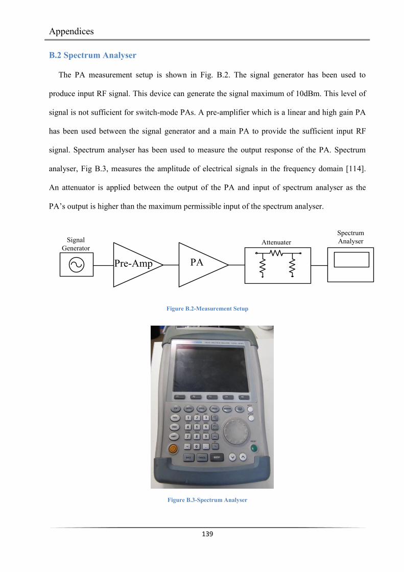
Appendices
139
B.2 Spectrum Analyser
The PA measurement setup is shown in Fig. B.2. The signal generator has been used to
produce input RF signal. This device can generate the signal maximum of 10dBm. This level of
signal is not sufficient for switch-mode PAs. A pre-amplifier which is a linear and high gain PA
has been used between the signal generator and a main PA to provide the sufficient input RF
signal. Spectrum analyser has been used to measure the output response of the PA. Spectrum
analyser, Fig B.3, measures the amplitude of electrical signals in the frequency domain [114].
An attenuator is applied between the output of the PA and input of spectrum analyser as the
PA’s output is higher than the maximum permissible input of the spectrum analyser.
Pre-Amp PA
Signal Generator
Spectrum AnalyserAttenuater
Figure B.2-Measurement Setup
Figure B.3-Spectrum Analyser

Appendices
Appendix C
Paper 1
“Analytical Solution for Switched Band Matching Networks”
F.Norouzian and P.Gardner
3rd Annual IET Seminar on Passive RF and Microwave Components, 2012
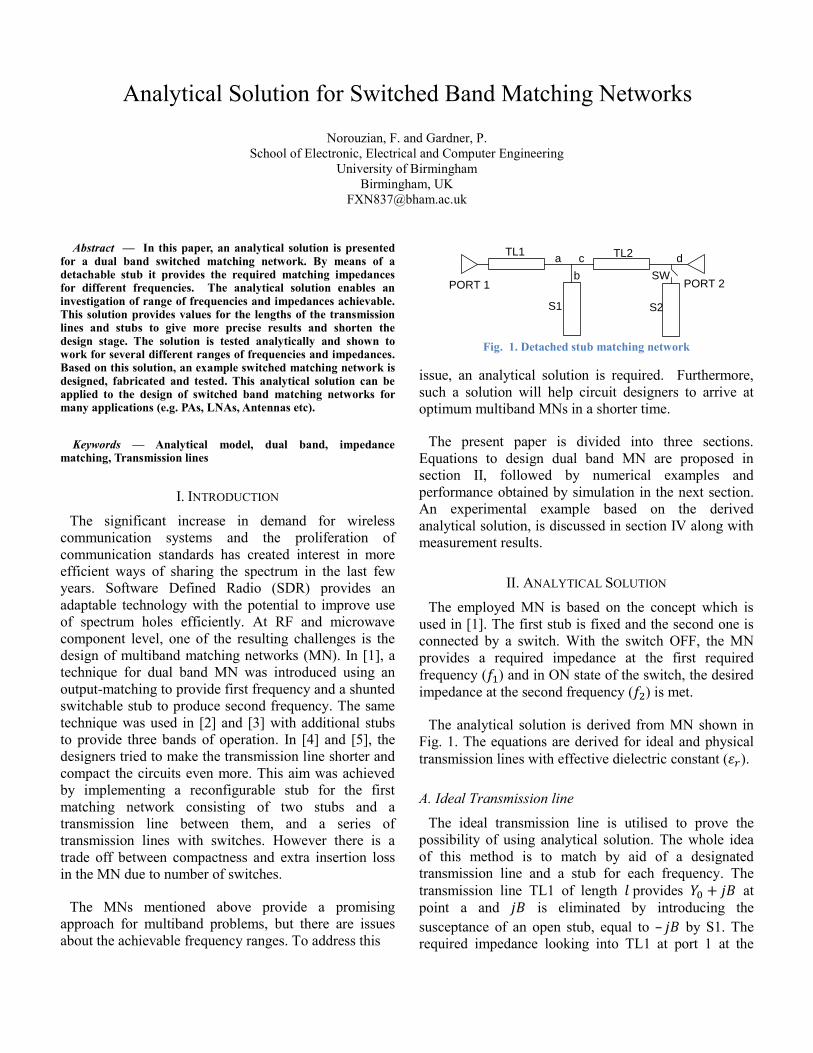
Analytical Solution for Switched Band Matching Networks
Norouzian, F. and Gardner, P. School of Electronic, Electrical and Computer Engineering
University of Birmingham Birmingham, UK
Abstract — In this paper, an analytical solution is presented
for a dual band switched matching network. By means of a detachable stub it provides the required matching impedances for different frequencies. The analytical solution enables an investigation of range of frequencies and impedances achievable. This solution provides values for the lengths of the transmission lines and stubs to give more precise results and shorten the design stage. The solution is tested analytically and shown to work for several different ranges of frequencies and impedances. Based on this solution, an example switched matching network is designed, fabricated and tested. This analytical solution can be applied to the design of switched band matching networks for many applications (e.g. PAs, LNAs, Antennas etc).
Keywords — Analytical model, dual band, impedance
matching, Transmission lines
I. INTRODUCTION
The significant increase in demand for wireless communication systems and the proliferation of communication standards has created interest in more efficient ways of sharing the spectrum in the last few years. Software Defined Radio (SDR) provides an adaptable technology with the potential to improve use of spectrum holes efficiently. At RF and microwave component level, one of the resulting challenges is the design of multiband matching networks (MN). In [1], a technique for dual band MN was introduced using an output-matching to provide first frequency and a shunted switchable stub to produce second frequency. The same technique was used in [2] and [3] with additional stubs to provide three bands of operation. In [4] and [5], the designers tried to make the transmission line shorter and compact the circuits even more. This aim was achieved by implementing a reconfigurable stub for the first matching network consisting of two stubs and a transmission line between them, and a series of transmission lines with switches. However there is a trade off between compactness and extra insertion loss in the MN due to number of switches.
The MNs mentioned above provide a promising approach for multiband problems, but there are issues about the achievable frequency ranges. To address this
a
b
cTL1 TL2
S1 S2
d
SWPORT 1 PORT 2
Fig. 1. Detached stub matching network
issue, an analytical solution is required. Furthermore, such a solution will help circuit designers to arrive at optimum multiband MNs in a shorter time.
The present paper is divided into three sections. Equations to design dual band MN are proposed in section II, followed by numerical examples and performance obtained by simulation in the next section. An experimental example based on the derived analytical solution, is discussed in section IV along with measurement results.
II. ANALYTICAL SOLUTION
The employed MN is based on the concept which is used in [1]. The first stub is fixed and the second one is connected by a switch. With the switch OFF, the MN provides a required impedance at the first required frequency ( ) and in ON state of the switch, the desired impedance at the second frequency ( ) is met.
The analytical solution is derived from MN shown in Fig. 1. The equations are derived for ideal and physical transmission lines with effective dielectric constant ( ).
A. Ideal Transmission line
The ideal transmission line is utilised to prove the possibility of using analytical solution. The whole idea of this method is to match by aid of a designated transmission line and a stub for each frequency. The transmission line TL1 of length provides at point a and is eliminated by introducing the susceptance of an open stub, equal to – by S1. The required impedance looking into TL1 at port 1 at the

first frequency is and defined as . At point a, admittance ( ) can be written as:
(1)
where and are the characteristic impedance and the electrical length of TL1, respectively.
Splitting into real part and imaginary part yields (2) and (3) respectively.
(2)
(3)
Given that the real part of is equal to the
characteristic admittance of the system, , the electrical length of the transmission line can be obtained by the following equation.
(4)
By substituting value back into (3), the susceptance
part of , , can be obtained. The value of can be eliminated by the open stub S1. The admittance at b in Fig. 1 is and should be equal to – . So the electrical length of the stub can be calculated by
(5)
To provide the desired impedance
at , the second stub is introduced into the circuit by turning the switch ON. To calculate the length of the second transmission line and stub (TL2 and S2 respectively), the admittance at c is calculated by (6).
(6)
The physical length of and are fixed but their
electrical lengths vary as the frequency changes; therefore,
and are introduced which are electrical
length of first transmission line and stub at , respectively. Following the same procedure by applying
instead of , we can calculate the electrical
lengths of and . The derived analytical solution is applicable for
multiband MNs. This can be done by adding additional switched stubs, position relative to , by repeated application of (6) and back to (3)-(5).
B. Physical Transmission line
For practical applications, the above introduced
algorithm needs to be implemented in a physical
transmission line medium such as microstrip. To find the
lengths of transmission lines in microstrip, the physical
lengths need to be divided by yielding (7) where
denotes effective dielectric constant.
(7)
III. NUMERICAL EXAMPLES
To verify the presented approach, the equations have been applied to several different numerical values in different ranges of frequencies and one of them is presented in this section. A Gallium Nitride (GaN) HEMT from Nitronex is chosen as an example. Two different frequencies are selected and appropriate impedances are obtained from load pull information in the device datasheet. The required impedances are and at and MHz, respectively. The MN has been designed so that the required impedance for the higher frequency is provided by the OFF state of the switch, since the amount of loss in switch in its ON state increases at higher frequency. Similar to previous section, appropriate lengths for the transmission lines and stubs are calculated in two different versions, ideal and physical transmission lines.
A. Ideal Transmission line
Using (3-5) the value of , and are calculated respectively. In next step is obtained using (6). Using the same procedure and are calculated. These results are used in the simulations and the simulation outputs are shown Fig. 2 (a), confirming good agreement with the required impedances taken from the device datasheet.
In the first frequency, one transmission line and one stub is used to match to the required impedance. The second desired impedance is converted to at point c in

Fig. 1. The second line and stub parameters are calculated to transform at the second frequency to at points c and d, respectively. No further iteration of the first line and stub are required to achieve this. The presented method proves that there is no forbidden region to match any dual frequencies by this MN, because whatever the value of , it can, in principle, be matched using a single line and stub.
(a) (b)
Fig. 2. Simulation result (a) ideal transmission line (b) physical transmission line
B. Physical Transmission line
The electrical lengths of the transmission lines in this case are evaluated as before and their physical lengths are found by use of (7). Fig. 2(b) shows the simulation results based on the calculated lengths.
The results show a perfect match at 1800MHz and a reasonably close match at 900MHz. The reason for the difference observed in second frequency is the discontinuity of the T-junction. One solution to resolve this issue is to optimize the MN to compensate the discontinuity effect of the T-junction. Taking into account the discontinuity and fine tuning the simulation will give the result presented in Fig. 3 that shows good agreement at 900 MHz.
Fig. 3. Simulation result after adjustments
VI. EXPERIMENTAL
The MN based on the calculation in the last part was built, to prove the validation of the algorithm. It was fabricated on microstrip substrate of thickness of 0.76 mm and relative dielectric constant of 3.5. A PIN diode was used as the switch because of its advantages such as low insertion loss, high isolation, high switching speed and excellent power handling at microwave frequencies [6]. The PIN diode was type BAR50 from Infineon.
The simulation and measurement results are compared and plotted by their magnitude (Fig. 4) and on the Smith Chart (Fig. 5). The markers on Fig. 5 ((a) and (b)) indicate the reflection coefficient at the intended frequencies for the ON and OFF state (1800 and 900 MHZ, respectively). Both graphs are shown good agreement between simulation and measurement. The small differences are due to real components and their tolerances.
Fig. 4. Simulated and measured S11 in (a) OFF and (b) ON state
V. CONCLUSION
In this contribution, for the first time, the feasibility of multiband MNs for different frequencies, by aid of derived equation, has been shown. The proposed theoretical approach, based on the detached stub MN, provides a closed-form and recursive solution to design dual-band MNs precisely, given any two frequencies. Furthermore this method can be applied not only for two
0 0.5 1 1.5 2 2.5 3
x 109
-30
-25
-20
-15
-10
-5
0
Frequency (Hz)
S11 [
dB
]
S11-Sim
S11-Meas
0 0.5 1 1.5 2 2.5 3
x 109
-16
-14
-12
-10
-8
-6
-4
-2
0
Frequency (Hz)
S11 [
dB
]
S11-Sim
S11-Meas
(b)
(a)

(a) (b)
Fig. 5. Simulated and measured input impedance of MN (a) OFF state and (b) On state
but for several band MNs. Numerical and experimental results have been presented by this work and the results were compared to prove the validity of the algorithm. The presented MNs and derived algorithm could be applied to a wide range of multiband components, such as antennas, LNAs and PAs. These promising results encourage further research on designing multiband MNs that take account of harmonic termination requirements, which are important in power amplifier applications. Investigation of nonlinearity caused by a PIN diode is also a matter of interest.
VI. REFERENCE [1] A. Fukuda, H. Okazaki, T. Hirota and Y. Yamao, “Novel 900
MHz/1.9 GHz Dual-Mode Power Amplifier Employing MEMS
Switches for Optimum Matching”, IEEE Microwave and
Wireless Components Letters, vol.14, no.3, pp. 121-123, March
2004. [2] A. Fukuda, H. Okazaki, S. Narahashi, T. Hirota and Y. Yamao,
“A 900/1500/200-MHz Triple-Band Reconfigurable Power
Amplifier Employing RF-MEMS Switches”, IEEE, pp. 657-660,
2005.
[3] H. M. Nemati, J. Grahn and C. Fager, “Band-Reconfigurable
LDMOS Power Amplifier”, in 40th European Microwave
Conference, 2010, pp.978-981.
[4] A. Fukuda, H. Okazaki and S. Narahashi, “A Novel Compact
Reconfigurable Quad-band Power Amplifir Employing RF-
MEMS switches”, in 36th European Microwave Conference,
2006, pp. 344-346.
[5] A. Fukuda, T. Furuta, H. Okazaki, S. Narahashi, “A 0.9-5-GHz
Wide-Range 1 W-Class Reconfigurable Power Amplifier
Employing RF-MEMS Switches”, IEEE, pp. 1859-1862, 2006.
[6] M. Watertown, The PIN Diode Circuit Designers’ Handbook,
Massachusetts: Microsemi Corporation, 1998.

Appendices
Paper 2
“Concurrent Dual-Band High Efficiency Class-E Power Amplifier”
F.Norouzian and P.Gardner
2013 European Microwave Integrated Circuits Conference (EuMIC),

Concurrent Dual-Band High Efficiency Class-E Power Amplifier
Fatemeh Norouzian School of Electronic, Electrical and Computer Engineering
University of Birmingham Birmingham, UK
Peter Gardner School of Electronic, Electrical and Computer Engineering
University of Birmingham Birmingham, UK
Abstract— In this paper, a concurrent dual-band class-E power amplifier is proposed. A distributed matching network is designed without any switch to achieve dual-mode operation. The power amplifier works in the 777-787 MHz and 1710-1785 MHz bands for LTE system. The measured results show 22 and 27 dBm output power at first and second band, respectively. This power amplifier obtains efficiency of 60% in lower bandwidth and 84.5 % in higher bandwidth. A novel matching network is also presented to switch between two different optimum operations for class-E design to improve the efficiency in the lower band.
Keywords—class-E; dual-band; high efficiency; power amplifier
I. INTRODUCTION The significant increase in demand for wireless
communication systems and the proliferation of communication standards has created interest in more efficient ways of sharing the spectrum in the last few years. Software Defined Radio (SDR) provides an adaptable technology with the potential to improve use of spectrum holes efficiently. The Power Amplifier (PA) is the most power consuming part in transmitters. Designing high efficiency multiband PAs is a critical research area.
Different multiband class-E PAs have been reported. Some of their features are summarized in table 1, [1]-[6]. Composite right/left-handed transmission lines (CRLH TLs) are used in [1] to provide dual-band amplification. In [2], MEMS are used to switch between two frequencies. A quad-band class-E PA is proposed in [3] which consists of four transistors and a single input/output matching network (MN). It works in one of the frequency bands at a time and is switched between bands by controlling the gate bias. Sub-optimum class-E operation is assumed in [4] with element values evaluated for a compromise between two bands. A multi-level switching resistance model is incorporated to switch between two frequencies in [5]. A dual-band class-E with finite DC-feed inductance is presented in [6]. A switch is applied to achieve optimum performance in the selected band, while the inductors are constant.
Class-E has highly frequency dependent characteristics. Therefore, designing a dual-band class-E PA is challenging
Table 1. Multiband class-E PAs
Reference Frequency band (GHz)
Output power (dBm)
Efficiency (%)
PAE (%)
[1] 0.836 /1.95 27 N.A 42 [2] 0.9/1.8 20 38/26 N.A
[3] 1.9/2.3/ 2.6/3.5
24.2/23.8/ 23.4/20.5 48/44/40/35 N.A
[4] L-/S-band 30/28 61/42 50/30 [5] 1.95/2.6 29/28 N.A 65/63 [6] 1.7/2.5 27 N.A 57
This work 0.782/1.748 22/27 60/84.5 55/72 because optimum output matching and harmonic elimination have to be achieved in both bands at the same time with a single output matching network (OMN) to satisfy the required efficiency and output power in both operating bands. In this paper, a dual-band class-E PA with high efficiency in both bands is presented. This PA is designed without switches to minimize the number of components and reduce the losses introduce by switches. The effect of the shunt capacitor across the transistor on efficiency is studied and a switched band MN is proposed to enable the OMN to switch between two optimum modes and improve efficiency further.
II. DUAL-BAND CLASS-E POWER AMPLIFIER The class-E PA was invented by Nathan and Alan Sokal in
the 1970s [7].The active device in class-E PA is operating as a switch; when the transistor is off, current flows through the shunt capacitance and in the on duration, current flows through the transistor. The OMN plays a crucial role in designing a highly efficient class-E PA. OMN includes a set of specific valued components at fundamental frequency to avoid any overlap between voltage and current waveforms; resulting in 100% efficiency, ideally. In practice some of the delivered power will appear in second and third harmonic frequencies. To maximize the efficiency, all harmonics should be open circuit. The transistor should be biassed at pinch off and driven into compression, so the transistor will be on for the forward cycle of sinusoidal input RF waveform and for all of the reverse cycle the transistor is switched off.
The first stage of designing a class-E PA is to calculate optimum parameters of OMN. Equations (3) to (6), taken from [7], are applied to provide values of components (i.e. load resistance R , shunt capacitance C , series capacitance and

inductance, 0C and 0L respectively). These equations are derived from a time domain equation, according to required voltage and current assumption across the transistor, in OFF and On state, respectively, (1) and (2).
0|)( TtD tV (1)
0|)(Tt
D
dttdV
(2)
These components are calculated based on specific supply voltage DV and required output power outP . Loaded quality factor ( LQ ) is a free choice variable and chosen by designers based on a tradeoff between operating bandwidth and rejection of harmonics. For having duty ratio of a usual choice, 50%, the minimum value of LQ is 1.7879. The most desirable range to provide acceptable efficiency and linearity is between 5 and 10.
2
2 402444.0451759.015768.0L
QQPVR
Lout
D (3)
DLL LQQRC 22
6.003175.191424.0144668.5
1
(4)
DLL LQQRC 20
2.07879.1
101468.11104823.011
(5)
RQL L0 (6)
The dual-band class-E PA presented in this work is
designed with a transmission line OMN based on two lumped element networks. Each lumped element network is designed to operate in one of the desired frequencies. As it is understandable from equations, the value of components will be different for each band of frequency, hence a simple lumped element matching network would require a switch. For that reason, a distributed OMN which works simultaneously in two different frequencies without switches has been proposed here to avoid losses of switch. Generally, transmission line MNs are preferred over using lumped elements as their practical implementation is more convenient and they have more reliable performances as well as less insertion loss. To fulfill the requirements of the two lumped element network using a single transmission line and stub, a required reflection coefficient has to be obtained from the two lumped element MN in the two operation frequency bands. A single transmission line and a single stub, tuned by width and length, have been used in the OMN to provide the same reflection coefficient as the lumped element networks at desired frequencies, Fig.1. Having only a single transmission line and a stub will enable working simultaneously in two frequencies and make the design more compact than substituting each component with their equivalent transmission line.
It has been shown that second harmonic termination is sufficient to have class-E performance to a reasonable approximation [8]. The second harmonic termination (HT)
is designed to behave as open circuit at drain of the transistor at both frequencies. The basic idea to terminate the harmonic frequencies is using a transmission line and
R
L C
PORT1 PORT2 PORT2PORT1
(a) (b)
Fig. 1. OMN (a) basic OMN for class-E (b) distributed OMN an open stub both with electrical length of λ⁄4, Fig. 2. Thus this block is composed of a transmission line and a stub which is λ⁄4 at the second harmonic of the higher frequency. To terminate the second harmonic of the lower frequency, a second λ⁄4 stub is required. Then another λ⁄4 transmission line is required to convert the short circuit to open circuit at port 1. This requirement is satisfied by the aid of the first transmission line, the first stub and an added transmission line (TL). By adjusting the length of TL, the cascaded line-stub-line combination can be made equivalent to an impedance inverter at that specific frequency. This harmonic termination circuit concept could be extended for terminating n harmonics with n transmission lines and stubs. The OMN and HT circuits are implemented together to provide the required performances for class-E operation.
The dual-band input matching network (IMN) is designed to have promising return loss in both desired bands.
III. SIMULATION AND MEASUREMENT This dual-band PA is designed for the LTE system to cover
two bands, 777-787 MHz and 1710-1785 MHz and output power of 23 dBm in both bands.
A. Simulation Components are calculated for both bands, based on
desired output power and voltage supply ( LQ set as 10). The calculated values are illustrated in table 2. A transmission line and stub are used to transform the 50 impedance of the transmitting antenna to the calculated load impedance, 62.45 . Then calculated capacitance and inductance for both bands are simulated to find out their reflection coefficient at the required frequencies to be used in designing the equivalent distributed version, Fig. 3.
In order to design this OMN practically, termination of the second harmonic frequencies is considered. Thus, the introduced HT circuit aims to provide open circuit at second harmonic frequencies of operating frequencies, 782 and 1748 MHz. The designed HT circuit is implemented with OMN. IMN is modeled to provide reasonable match at both frequency bands, by the aid of a transmission line and two stubs.
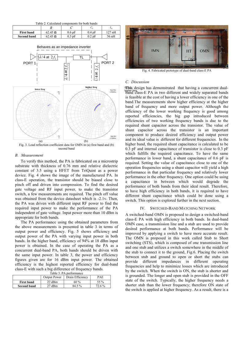
Table 2. Calculated components for both bands R C 0C
0L
First band 62.45 0.6 pF 0.4 pF 127 nH Second band 62.45 0.3 pF 0.2 pF 56 nH
TL
PORT 1 PORT 2
4/ at 22 f
4/
at
22
f
4/
at
12
f
Behaves as an impedance inverter
Fig. 2. Harmonic termination circuit
0 1.0
1.0
-1.0
10.0
10.0
-10.0
5.0
5.0
-5.0
2.0
2.0
-2.0
3.0
3.0
-3.0
4.0
4.0
-4.0
0.2
0.2
-0.2
0.4
0.4
-0.4
0.6
0.6
-0.6
0.8
0.8
-0.8
lower freqSwp Max
787MHz
Swp Min
777MHz
S(1,1)lower freq
0 1.0
1.0
-1.0
10.0
10.0
-10.0
5.0
5.0
-5.0
2.0
2.0
-2.0
3.0
3.0
-3.0
4.0
4.0
-4.0
0.2
0.2
-0.2
0.4
0.4
-0.4
0.6
0.6
-0.6
0.8
0.8
-0.8
higher freqSwp Max
1785MHz
Swp Min
1710MHz
S(1,1)higher freq
(a) (b)
Fig. 3. Load reflection coefficient data for OMN in (a) first band and (b) second band
B. Measurement To verify this method, the PA is fabricated on a microstrip
substrate with thickness of 0.76 mm and relative dielectric constant of 3.5 using a HFET from TriQuint as a power device. Fig. 4 shows the image of the manufactured PA. In class-E operation, the transistor should be biased close to pinch off and driven into compression. To find the desired gate voltage and RF input power, to make the transistor switch, a few measurements are required. The pinch off value was obtained from the device datasheet which is -2.1v. Then, the PA was driven with different input RF power to find the required input power to make the performance of the PA independent of gate voltage. Input power more than 10 dBm is appropriate for both bands.
The PA performance using the obtained parameters from the above measurements is presented in table 3 in terms of output power and efficiency. Fig. 5 shows efficiency and output power of the PA with varying input power in both bands. In the higher band, efficiency of 94% at 18 dBm input power is obtained. In the case of operating the PA as a concurrent dual-band PA, both bands should be driven with the same input power. In table 3, the power and efficiency figures given are for 16 dBm input power. The obtained efficiency is the highest reported efficiency for dual-band class-E with such a big difference of frequency bands.
Table 3. PA performance Output Power Drain Efficiency PAE
First band 22 dBm 60 % 55 % Second band 27 dBm 84.5 % 72.6 %
Fig. 4. Fabricated prototype of dual-band class-E PA
C. Discussion This design has demonstrated that having a concurrent dual-band class-E PA in two different and widely separated bands is feasible at the cost of having a lower efficiency in one of the band.The measurements show higher efficiency at the higher band of frequency and more output power. Although the efficiency of the lower working frequency is good among reported efficiencies, the big gap introduced between efficiencies of two working frequency bands is due to the required shunt capacitor across the transistor. The value of shunt capacitor across the transistor is an important component to produce desired efficiency and output power and its ideal value is different for different frequencies. In the higher band, the required shunt capacitance is calculated to be 0.3 pF and internal capacitance of transistor is close to 0.3 pF which fulfills the required capacitance. To have the same performance in lower band, a shunt capacitance of 0.6 pF is required. Setting the value of capacitance close to one of the operation frequencies using a shunt capacitor will yield a high performance in that particular frequency and relatively lower performance in the other frequency. One option could be using a capacitance in between which would degrade the performance of both bands from their ideal result. Therefore, to have high efficiency in both bands, it is required to have different shunt capacitance which could be done using a switch. This option is explored further in the next section.
IV. SWITCHED-BAND MATCHING NETWORK A switched-band OMN is proposed to design a switched-band class-E PA with high efficiency in both bands. In dual-band OMN case, a transmission line and a stub are used to provide desired performance at both bands. Performance will be improved by applying a switch to have more accurate result. The OMN is proposed in this work called Stub to Short switching (STS), which is composed of one transmission line and one stub and utilizes a switch somewhere in the middle of the stub to connect it to the ground, Fig.6. Placing the switch between stub and ground to open or short the stubs can provide different impedances in different operating frequencies and help to minimize losses which are introduced by the switch. When the switch is ON, the stub is shorter and is grounded. The longer and open stub is provided in the OFF state of the switch. Typically, the higher frequency needs a shorter stub than the lower frequency; therefore ON state of the switch is applied at higher frequency. As a result, there is a
IMN HT OMN
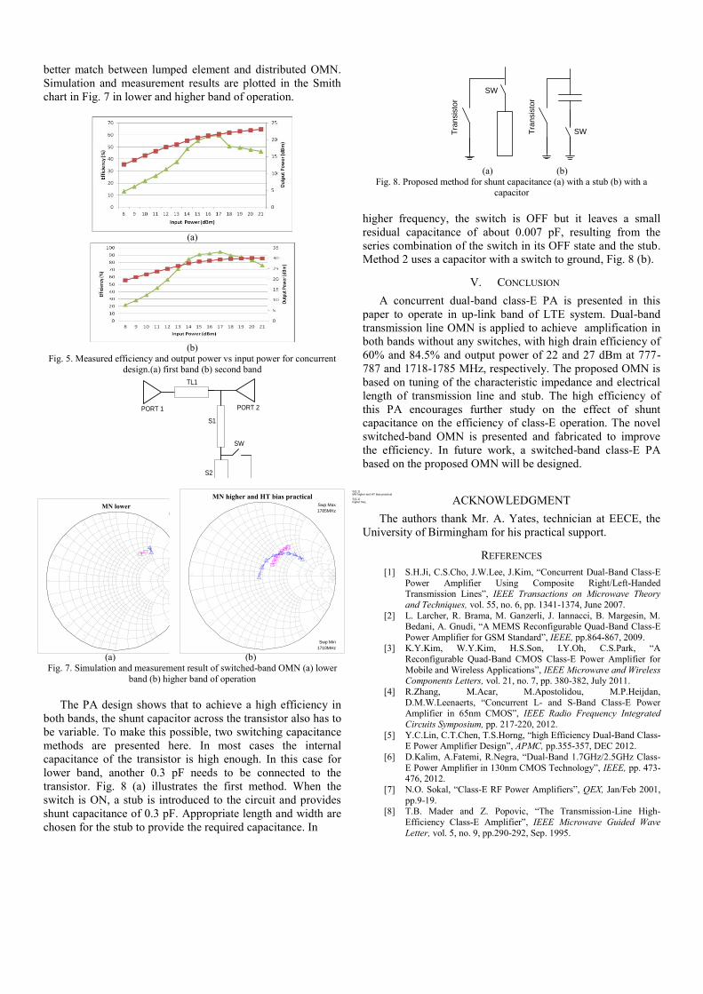
better match between lumped element and distributed OMN. Simulation and measurement results are plotted in the Smith chart in Fig. 7 in lower and higher band of operation.
(a)
(b)
Fig. 5. Measured efficiency and output power vs input power for concurrent design.(a) first band (b) second band
S1
S2
TL1
PORT 1 PORT 2
SW
Fig. 6. Switched-band OMN
0 1.0
1.0
-1.0
10.0
10.0
-10.0
5.0
5.0
-5.0
2.0
2.0
-2.0
3.0
3.0
-3.0
4.0
4.0
-4.0
0.2
0.2
-0.2
0.4
0.4
-0.4
0.6
0.6
-0.6
0.8
0.8
-0.8
MN lowerSwp Max
787MHz
Swp Min
777MHz
S(1,1)MN lower
S(1,1)lower freq
0 1.0
1.0
-1.0
10.0
10.0
-10.0
5.0
5.0
-5.0
2.0
2.0
-2.0
3.0
3.0
-3.0
4.0
4.0
-4.0
0.2
0.2
-0.2
0.4
0.4
-0.4
0.6
0.6
-0.6
0.8
0.8
-0.8
MN higher and HT bias practicalSwp Max
1785MHz
Swp Min
1710MHz
S(1,1)MN higher and HT bias practical
S(1,1)higher freq
(a) (b) Fig. 7. Simulation and measurement result of switched-band OMN (a) lower
band (b) higher band of operation
The PA design shows that to achieve a high efficiency in both bands, the shunt capacitor across the transistor also has to be variable. To make this possible, two switching capacitance methods are presented here. In most cases the internal capacitance of the transistor is high enough. In this case for lower band, another 0.3 pF needs to be connected to the transistor. Fig. 8 (a) illustrates the first method. When the switch is ON, a stub is introduced to the circuit and provides shunt capacitance of 0.3 pF. Appropriate length and width are chosen for the stub to provide the required capacitance. In
Tra
nsis
tor
SW
Tra
nsis
tor
SW
(a) (b)
Fig. 8. Proposed method for shunt capacitance (a) with a stub (b) with a capacitor
higher frequency, the switch is OFF but it leaves a small residual capacitance of about 0.007 pF, resulting from the series combination of the switch in its OFF state and the stub. Method 2 uses a capacitor with a switch to ground, Fig. 8 (b).
V. CONCLUSION A concurrent dual-band class-E PA is presented in this
paper to operate in up-link band of LTE system. Dual-band transmission line OMN is applied to achieve amplification in both bands without any switches, with high drain efficiency of 60% and 84.5% and output power of 22 and 27 dBm at 777-787 and 1718-1785 MHz, respectively. The proposed OMN is based on tuning of the characteristic impedance and electrical length of transmission line and stub. The high efficiency of this PA encourages further study on the effect of shunt capacitance on the efficiency of class-E operation. The novel switched-band OMN is presented and fabricated to improve the efficiency. In future work, a switched-band class-E PA based on the proposed OMN will be designed.
ACKNOWLEDGMENT The authors thank Mr. A. Yates, technician at EECE, the
University of Birmingham for his practical support.
REFERENCES [1] S.H.Ji, C.S.Cho, J.W.Lee, J.Kim, “Concurrent Dual-Band Class-E
Power Amplifier Using Composite Right/Left-Handed Transmission Lines”, IEEE Transactions on Microwave Theory and Techniques, vol. 55, no. 6, pp. 1341-1374, June 2007.
[2] L. Larcher, R. Brama, M. Ganzerli, J. Iannacci, B. Margesin, M. Bedani, A. Gnudi, “A MEMS Reconfigurable Quad-Band Class-E Power Amplifier for GSM Standard”, IEEE, pp.864-867, 2009.
[3] K.Y.Kim, W.Y.Kim, H.S.Son, I.Y.Oh, C.S.Park, “A Reconfigurable Quad-Band CMOS Class-E Power Amplifier for Mobile and Wireless Applications”, IEEE Microwave and Wireless Components Letters, vol. 21, no. 7, pp. 380-382, July 2011.
[4] R.Zhang, M.Acar, M.Apostolidou, M.P.Heijdan, D.M.W.Leenaerts, “Concurrent L- and S-Band Class-E Power Amplifier in 65nm CMOS”, IEEE Radio Frequency Integrated Circuits Symposium, pp. 217-220, 2012.
[5] Y.C.Lin, C.T.Chen, T.S.Horng, “high Efficiency Dual-Band Class-E Power Amplifier Design”, APMC, pp.355-357, DEC 2012.
[6] D.Kalim, A.Fatemi, R.Negra, “Dual-Band 1.7GHz/2.5GHz Class-E Power Amplifier in 130nm CMOS Technology”, IEEE, pp. 473-476, 2012.
[7] N.O. Sokal, “Class-E RF Power Amplifiers”, QEX, Jan/Feb 2001, pp.9-19.
[8] T.B. Mader and Z. Popovic, “The Transmission-Line High-Efficiency Class-E Amplifier”, IEEE Microwave Guided Wave Letter, vol. 5, no. 9, pp.290-292, Sep. 1995.


![Suspended Metasurface Loaded Dual Band Dual Polarized ... › proceedings › procAP19 › papers2019 › PID5638363.pdf · filter. In [9], a dual band dual polarized antenna is](https://static.fdocuments.in/doc/165x107/5f14de5c84dbd949e06a47a4/suspended-metasurface-loaded-dual-band-dual-polarized-a-proceedings-a-procap19.jpg)