
CSP Enhancement Mode Power MOSFET
6
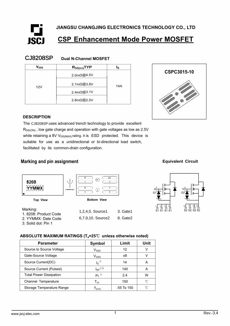
Dual N-Channel MOSFET DESCRIPTION V SSS Equivalent Circuit 1 The uses advanced trench technology to provide excellent R SS(ON) , low gate charge and operation with gate voltages as low as 2.5V while retaining a 8V V GS(MAX) rating. It is ESD protected. This device is suitable for use as a unidirectional or bi-directional load switch, facilitated by its common-drain configuration. CSPC30 15-10 Marking and pin assignment Symbol Parameter Limit Unit V SSS Source to Source Voltage 12 V V GSS ±8 V I S Source Current(DC) 14 A I SP Source Current (Pulsed) A P T W T ch Channel Temperature 150 ℃ T STG Storage Temperature Range -55 To 150 ℃ CJ8208SP Top View G1 S1 G2 S1 Gate-Source Voltage JIANGSU CHANGJING ELECTRONICS TECHNOLOGY CO., LTD CSP Enhancement Mode Power MOSFET www.jscj-elec.com CJ8208SP 1,2,4,5. Source1 3. Gate1 6,7,9,10. Source2 8. Gate2 S1 S1 S2 S2 S2 S2 1 2 4 5 6 7 9 10 3 8 Bottom View Rev.-3.4 Total Power Dissipation 2.4 140 ① ① ② ① ABSOLUTE MAXIMUM RATINGS (T a =25℃ unless otherwise noted) R SS(on) TYP I S 12V 14A 2.0mΩ@4.5V 2.1mΩ@3.8V 2.4mΩ@3.1V 2.8mΩ@2.5V Marking: 1. 8208: Product Code 2. YYMMX: Date Code 3. Solid dot: Pin 1
Transcript of CSP Enhancement Mode Power MOSFET
Dual N-Channel MOSFET
DESCRIPTION
VSSS
Equivalent Circuit
1
The uses advanced trench technology to provide excellent RSS(ON) , low gate charge and operation with gate voltages as low as 2.5V while retaining a 8V VGS(MAX) rating. It is ESD protected. This device is suitable for use as a unidirectional or bi-directional load switch, facilitated by its common-drain configuration.
CSPC30 15-10
Marking and pin assignment
SymbolParameter Limit UnitVSSS Source to Source Voltage 12 V
VGSS ±8 V
IS Source Current(DC) 14 A
ISP Source Current (Pulsed) A
PT W
TchChannel Temperature 150
TSTG Storage Temperature Range -55 To 150
CJ8208SP
Top View
G1
S1
G2
S1
Gate-Source Voltage
JIANGSU CHANGJING ELECTRONICS TECHNOLOGY CO., LTD
CSP Enhancement Mode Power MOSFET
www.jscj-elec.com
CJ8208SP
1,2,4,5. Source1 3. Gate1
6,7,9,10. Source2 8. Gate2
S1 S1 S2S2 S2 S21 2 4 5 6 7 9 10
3 8
Bottom View
Rev.-3.4
Total Power Dissipation 2.4
140
①
① ②
①
ABSOLUTE MAXIMUM RATINGS (Ta=25 unless otherwise noted)
R SS(o n) TYP I S
12V 14A
2.0mΩ@4.5V
2.1mΩ@3.8V
2.4mΩ@3.1V
2.8mΩ@2.5V
Marking:1. 8208: Product Code2. YYMMX: Date Code3. Solid dot: Pin 1

2
SymbolParameter Condition Min Typ Max Unit
Static Parameters
BVSSS Source to Source Breakdown Voltage ,VGS=0V 12 V
ISSS Zero-Gate Voltage Source Current VSS=10V,VGS=0V μA
IGSS Gate to Source Leakage Current VSS=0V, VGS= ±8V ±10 μA
VTHGate to Source Threshold Voltage VSS=10V, IS=1.11mA
VGS=4.5V,IS=3A
2.4 mΩ RSS(on)
Source to Source On-state
Resistance
mΩ
td(on)Turn-on Delay Time
tr Turn-on Rise Time
td(off) Turn-off Delay Time
tfTurn-off Fall Time
VSS=10V,IS=6A,VGS=4.5V
VF(S-S) Diode Forward Voltage VGS=0V,IS=6A 1.3 V
MOSFET ELECTRICAL CHARACTERISTICS
IS=1mA
2.1
www.jscj-elec.com
mΩ
μS
μSμS
μS
0.75
2.0
Rev.-3.4
2.5
8
3.5
17.5
mΩ
VDD=10V,RL=3.3Ω VGS=4.5V
1.0
1.1
1.3
1.6 2.8 6.15
2.9
2.8
V
1
aT =25 unless otherwise specified
VGS=3.8V,IS=3A
VGS=3.1V,IS=3A
VGS=2.5V,IS=3A
Notes: 1.Mounted on FR4 board (25.4mm25.4mmt1.0mm) using the minimum recommended pad size (36um Copper ).
G2
D2
S2
G1
D1
S1
VDD=10VIS=3ARL=3.3
Vout
Vin
PW=100μS
Ω
D=1%
10 %
90 %
90 %
10 %
90 %
10 %
td(on) tr td(off) tf
Vin
Vout
4.5V
2.t = 10 ms , Duty Cycle = 1 %.3.When FET1 is measured,G2 and S2 are short-circuited.
4.When FET1 is measured, FET2 is biased with VG2S2=4.5V.
0.35 1.4
4.0
④
CissInput Capacitance
Coss Output Cpacitance
Crss Reverse Transfer Capacitance
pF
pFpF
1560620
261
VSS=10V,VGS=0V, f=100kHz
Qg
Gate1-source1 chargeGate1-source2 charge
Total gate charge nC
nCnC
32.54.8
1.4
③
③
③
③
③
Qg1s1 Qg1s2
③
③

0.0 0.3 0.6 0.9 1.2 1.50
3
6
9
12
15
0.0 0.2 0.4 0.6 0.80.01
0.1
1
10
0 2 4 6 80
2
4
6
8
10
0.00 0.01 0.02 0.03 0.04 0.050
2
4
6
8
10
12
14
Pulsed
SO
UR
CE
CU
RR
EN
T
I S
(A
)
GATE TO SOURCE VOLTAGE VGS
(V)
IS VGS
TJ=125,85,25,-40
VF
Pulsed
DIO
DE
FO
RW
AR
D C
UR
RE
NT
CU
RR
EN
T
I F
(A)
BODY DIODE FORWARD VOLTAGE VF (V)
IF ——
RSS(ON)
—— VGS
ON
-RE
SIS
TA
NC
E
RS
S(O
N)
(m
)
GATE TO SOURCE VOLTAGE VGS
(V)
PulsedIS=3A
IS
——RSS(ON)
Pulsed
VGS=4.5V,3.8V,3.1V,2.5V
IS VSS
SO
UR
CE
CU
RR
EN
T
I S
(A
)
SOURCE TO SOURCE VOLTAGE VSS
(V)
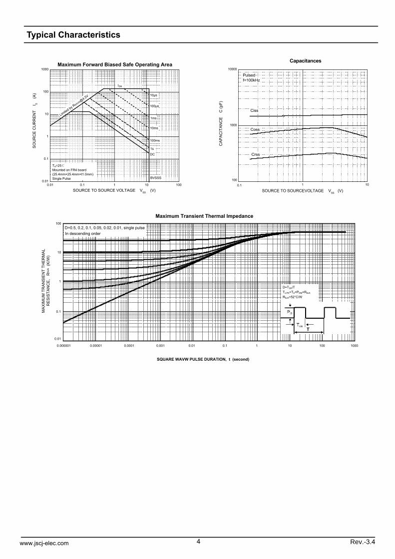
Typical Characteristics
2 861.5
2.0
2.5
3.0
3.5
VGS=2.5V
Pulsed
ON
-RES
ISTA
NC
E
RSS
(ON
) (m
)
4SOURCE CURRENT IS (A)
VGS=4.5V
VGS=3.8V
VGS=3.1V
TJ=25
Ta=25
VSS=5V
— —— —
TJ=125 85 25
1
3www.jscj-elec.com Rev.-3.4
TJ=125
85
25
1.0
20
-40
-40
0 5 10 15 20 25 30 350.0
0.5
1.0
1.5
2.0
2.5
3.0
3.5
4.0
4.5
Pulsed
Gate Charge
THR
ESH
OLD
VO
LTAG
E
V TH
(V)
GATE CHARGE Qg (nC)
VSS=10V
0.000001 0.00001 0.0001 0.001 0.01 0.1 1 10 100 1000
0.01
MAX
IMUM
TR
ANSI
ENT
THER
MAL
R
ESIS
TAN
CE,
R
θJA
(K/
W)
SQUARE WAVW PULSE DURATION, t (second)
Maximum Transient Thermal Impedance
D=Ton/TTJ,PK=TA+PDM×RθJA
RθJA=52°C/W
D=0.5, 0.2, 0.1, 0.05, 0.02, 0.01, single pulseIn descending order
0.1
1
10
100
0.01 1000.01
0.1
1
10
100
1000Maximum Forw ard Biased Safe Operating Area
SOURCE
CU
RR
ENT
I S
(A
)
0.1 1 10
SOURCE TO SOURCE VOLTAGE VSS (V)
BVSSS
DC1s
100ms
10ms
1ms
100μs
10μs
4www.jscj-elec.com Rev.-3.4
Typical Characteristics
Limited by RSSON@
4.5V
ISM
TA=25Mounted on FR4 board (25.4mm×25.4mm×t1.0mm) Single Pulse
0.1 10
100
1000
10000
Crss
Coss
Ciss
Pulsedf=100kHz
CA
PA
CIT
AN
CE
C
(pF
)
1
SOURCE TO SOURCEVOLTAGE VSS
(V)
Capaci tances

5
CSPC30 15-10
CSPC30 15-10
www.jscj-elec.com
NOTICE JSCJ reserves the rights to make modifications, enhancements, improvements, corrections or other changes without further notice to any product herein. JSCJ does not assume any liabilities arising out of the application or use of any product described herein.
Rev.-3.4
3.01±0.03
1.52±0.03
0.610
0.02225
0.11±0.022

Attention:
1、When exporting the products or technology described in this document, you should comply with the applicable export control laws
and regulations and follow the procedures required by such laws and regulations.
2、The products described in this book are intended to be used for general applications (such as office equipment, communications
equipment, measuring instruments and household appliances), or for specific applications as expressly stated in this book. Consult our
sales staff in advance for information on the following applications: Special applications (such as for airplanes, aerospace, automotive
equipment, traffic signaling equipment, combustion equipment, life support systems and safety devices) in which exceptional quality
and reliability are required, or if the failure or malfunction of the products may directly jeopardize life or harm the human body. It is to
be understood that our company shall not be held responsible for any damage incurred as a result of or in connection with your using
the products described in this book for any special application, unless our company agrees to your using the products in this book for
any special application.
3、Specifications of any and all JSCJ products described or contained herein stipulate the performance, characteristics, and functions
of the described products in the independent state, and are not guarantees of the performance, characteristics, and functions of the
described products as mounted in the customer’s products or equipment. To verify symptoms and states that cannot be evaluated in an
independent device, the customer should always evaluate and test devices mounted in the customer’s products or equipment.
4、You should use the JSCJ products described in this document within the range specified by JSCJ, especially with respect to the
maximum rating, operating supply voltage range, movement power voltage range, heat radiation characteristics, installation and other
product characteristics. JSCJ shall have no liability for malfunctions or damages arising out of the use of JSCJ products beyond such
specified ranges.
5、Regarding monolithic semiconductors, if you should intend to use this IC continuously under high temperature, high current, high
voltage, or drastic temperature change, even if it is used within the range of absolute maximum ratings or operating conditions, there is
a possibility of decrease reliability. Please contact us for a confirmation.
6、JSCJ strives to supply high-quality high-reliability products. However, any and all semiconductor products fail with some
probability. It is possible that these probabilistic failures could give rise to accidents or events that could endanger human lives, that
could give rise to smoke or fire, or that could cause damage to other property. When designing equipment, adopt safety measures so
that these kinds of accidents or events cannot occur. Such measures include but are not limited to protective circuits and error
prevention circuits for safe design, redundant design, and structural design.
7、No part of this publication may be reproduced or transmitted in any form or by any means, electronic or mechanical, including
photocopying and recording, or any information storage or retrieval system, or otherwise, without the prior written permission of
CHANGJING ELEC.TECH.
8、JSCJ has used reasonable care in preparing the information included in this document, but JSCJ does not warrant that such
information is error free. JSCJ assumes no liability whatsoever for any damages incurred by you resulting from errors in or omissions
from the information included herein.
9、The products and product specifications described in this book are subject to change without notice for modification and/or
improvement. At the final stage of your design, purchasing, or use of the products, therefore, ask for the most up-to-date Product
Standards in advance to make sure that the latest specifications satisfy your requirements.
This catalog provides information as of May 2021. Specifications and information herein are subject to change without notice.
6www.jscj-elec.com Rev.-3.4


![BAB II TINJAUAN PUSTAKAeprints.umm.ac.id/35672/3/jiptummpp-gdl-arirobiuli-48901... · 2017-11-14 · 10 Gambar 2.6 Simbol Transistor MOSFET Mode Enhancement [9]. (a). N-Channel Enhancement](https://static.fdocuments.in/doc/165x107/5e9da1fd111da33d79475dc0/bab-ii-tinjauan-2017-11-14-10-gambar-26-simbol-transistor-mosfet-mode-enhancement.jpg)


