Coventor Overview - ednc.com · Serving the World Leaders in MEMS and Semiconductors IDMs Fabless...
14
Coventor Overview
-
Upload
trinhnguyet -
Category
Documents
-
view
217 -
download
0
Transcript of Coventor Overview - ednc.com · Serving the World Leaders in MEMS and Semiconductors IDMs Fabless...

Coventor Overview

Company Overview
Coventor History:
Founded in 1996
Expertise in 3D modeling and simulation
Initially focused on tools for MEMS design
Focus:
Provide 3D solutions to the MEMS and
semiconductor industries that harness
compute power to dramatically reduce
physical prototyping
Privately Held
• Needham Capital
• Intel Capital
Slide 2
Headquarters — Cary, NC
Development centers • Waltham, Massachusetts
• Paris, France
Global sales and support

Leadership Team
Slide 3
Mike Jamiolkowski
President and CEO, Founder
18 years, founded ISS EDA company
Highly experienced team,
many years at Coventor and
serving the MEMS industry
Steve Breit, PhD
VP, Engineering
14 years
David Fried, PhD
CTO, Semiconductor
2 years +
14 years IBM
Tom Flynn
VP, Worldwide Sales
4 years +
14 years Ansoft
Ken Greiner
Director,
SEMulator3D R&D
16 years
Gunar Lorenz, PhD
Director,
MEMS+ R&D
14 years
Matt Kamon, PhD
Principal Technologist,
Simulation R&D
16 years
Chris Welham, PhD
Manager,
Applications Eng.
15 years
Gerold Schropfer, PhD
Director, Europe and
Foundry Program
13 years

Serving the World Leaders in
MEMS and Semiconductors
Foundries & Others IDMs Fabless Companies
Growing number of customers purchase both
MEMS and semiconductor solutions from Coventor
Semiconductor
MEMS
Slide 4
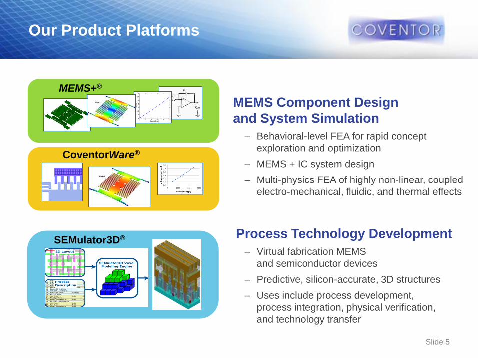
Our Product Platforms
MEMS Component Design
and System Simulation
– Behavioral-level FEA for rapid concept
exploration and optimization
– MEMS + IC system design
– Multi-physics FEA of highly non-linear, coupled
electro-mechanical, fluidic, and thermal effects
Process Technology Development
– Virtual fabrication MEMS
and semiconductor devices
– Predictive, silicon-accurate, 3D structures
– Uses include process development,
process integration, physical verification,
and technology transfer
MEMS+®
CoventorWare®
SEMulator3D®
Slide 5

The Traditional Approach
to MEMS Design
ASIC Design
MEMS Design
Fab / Foundry
MEMS Process Learning Cycle
MEMS Process Learning Cycle
MEMS Process Learning Cycle
MEMS ProcessLearning Cycle
Control System Design Control System Design Control System Design
Conventional FEA
Conventional FEA Conventional FEA Conventional FEA
Modeling Modeling Modeling Modeling
IC Design IC Design IC Design
Over-simplified
Too slow to inform fab cycles Full coupling infeasible
Hand-crafted
Design-specific
Consequence: too many “build and test” cycles
Slide 6

MEMS+ is a New Approach
ASIC Design
MEMS Design
Fab / Foundry
MEMS Process Learning Cycle
MEMS Process Learning Cycle
Control System Design
Conventional FEA
Modeling
IC Design
Complementary, for details and verifying MEMS+
Automatically generated, tunable accuracy vs. speed
Industrial strength,
Fast AND Accurate,
Full coupling feasible
Result: fewer “build and test” cycles
MEMS+, A Different Kind of FEA Rapid Design Studies Optimization Manufacturability
MEMS and IC co-design
Slide 7

MEMS+ Analysis of
Manufacturing Sensitivity
Slide 8
SOI MEMS process, 3 input variables
CD Thickness
Sidewall
Angle
Sense
mode
Functional spec:
sense mode frequency
No. o
f S
am
ple
s
Sense mode frequency (Hz) 7 sec per sample, less than 2 hrs total!
CD Offset Thickness Sidewall Angle
No
. o
f S
am
ple
s
Monte Carlo study, 1000 samples

MEMS+ Reference - Murata
Tero Sillanpää , Murata ASIC Design Manager:
“The Verilog-A Reduced Order Model (ROM)
exported from MEMS+ captures second-order
effects not seen in basic hand-crafted models
without any compromise in simulation
performance. We were able to create a Verilog-A
ROM of a complex gyro design in just a few
minutes, allowing our ASIC team to work in
parallel with the MEMS team on further design
iterations. Transient simulations in Cadence
showed that the model maintained the expected
modal frequencies and was stable. The robust
model exchange between MEMS and ASIC
designers enabled by MEMS+ reduces the
probability of design error and can help avoid
costly redesign iterations needed to address
unexpected behavior.”
Slide 9

What is SEMulator3D?
A Powerful Virtual Fabrication Platform for MEMS and Semiconductors
• Applicable to any process & any layout
• Handles complete process sequences and large areas
• Provides 3D structural models that are accurate, not idealized
• Provides predictive insights on design/technology interactions, saving “build-and-test” cycles
Layout Editor:
Design, OPC,…
Process Editor:
Step-by-Step Process
Behavioral Description
3D Viewer:
MEMS display
mirror on SRAM
Slide 10

Virtual Fabrication:
Uses for MEMS
Slide 11
Process Development: Predict/diagnose process problems
Issue: unexpected voids SEMulator3D model
confirms root cause
Physical Verification: Check structures, release completion, electrical continuity
Incomplete release etch Design error passed 2D DRC
Communication: Visualize, Animate process, DesignersFab/Foundry, Tech transfer
3-axis gyro
from chipworks teardown View details, cross section
Yield Optimization:
DRIE Quantify sensitivity of structure
CDs to process parameters
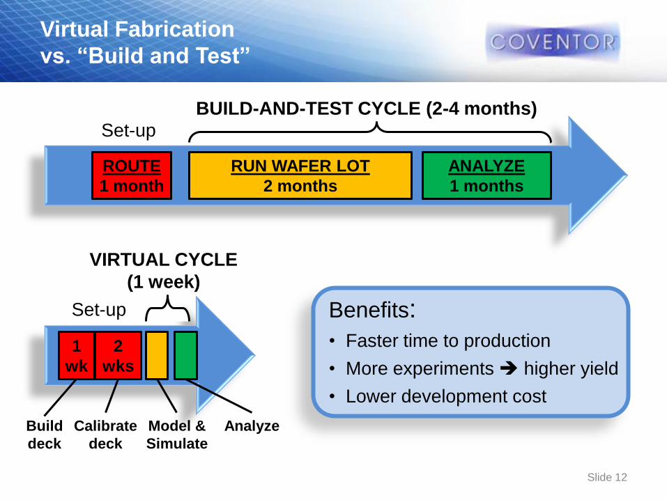
Virtual Fabrication
vs. “Build and Test”
ROUTE
1 month
RUN WAFER LOT
2 months
ANALYZE
1 months
Set-up
BUILD-AND-TEST CYCLE (2-4 months)
2
wks
1
wk
Build
deck
Calibrate
deck
VIRTUAL CYCLE
(1 week)
Model &
Simulate
Analyze
Benefits: • Faster time to production
• More experiments higher yield
• Lower development cost
Set-up
Slide 12

Virtual Fabrication
for MEMS Foundries
MEMS foundries use SEMulator3D for:
• Process development: Predict and
diagnose process issues and improve yield
• Physical design verification: Verify
structures, release and electrical continuity
before tape out
• Customer support: communicate process
and design and information with customers
• Failure analysis
“SEMulator3D gives engineers the ability to do virtual test runs to verify that a device design is compatible with the manufacturing process, and that the 3D result is as expected. Design mistakes and shortcomings can be identified, even if they are compatible with 2D layout rules.”
“The benefits of visualizing accurate 3-D virtual MEMS prototypes include increased probability of achieving first-time success by minimizing analysis errors, increased design efficiency by identifying process errors early, avoiding undesired effects that would have reduced yield, and more efficient communication between design engineers and outside groups.”
Slide 13

In Conclusion:
Most MEMS industry leaders are Coventor customers
• IDMs, Fabless, Foundries, R&D Organizations, Universities
Coventor’s unique product platform speeds time to market
• MEMS+ enables rapid design exploration, optimization,
and automated hand-off between MEMS and IC designers
• CoventorWare for specialized coupled physics challenges
• SEMulator3D for process development and sign-off
Coventor is well positioned to enable industry trends
• Continued growth from mobile and consumer applications
• New devices and new applications (passive displays, IR imaging,…)
• Growth of the Fabless/Independent Foundry business model
Slide 14