
Controllable growth and flexible optoelectronic devices of ...
7
ISSN 1998-0124 CN 11-5974/O4 2019, 12(1): 000–000 https://doi.org/10.1007/s12274-020-2841-6 Research Article Controllable growth and flexible optoelectronic devices of regularly- assembled Bi 2 S 3 semiconductor nanowire bifurcated junctions and crosslinked networks Yi Hu 1 , Lingyun Mao 1 , Xin Yuan 1 , Jingyu Lu 1 , Renpeng Chen 1 , Tao Chen 1 , Wenjun Zhang 1 , Xiaolan Xue 1 , Wen Yan 1 , Mohammadreza Shokouhimehr 2 , Xiao Li Zhang 3 , and Zhong Jin 1,4 ( ) 1 Key Laboratory of Mesoscopic Chemistry of MOE, Jiangsu Key Laboratory of Advanced Organic Materials, School of Chemistry and Chemical Engineering, Nanjing University, Nanjing 210023, China 2 Department of Materials Science and Engineering, Research Institute of Advanced Materials, Seoul National University, Seoul 08826, Republic of Korea 3 School of Materials Science and Engineering, Zhengzhou University, Zhengzhou 450001, China 4 Shenzhen Research Institute of Nanjing University, Shenzhen 518063, China © Tsinghua University Press and Springer-Verlag GmbH Germany, part of Springer Nature 2020 Received: 20 December 2019 / Revised: 22 April 2020 / Accepted: 30 April 2020 ABSTRACT Regularly assembled structures of nanowires, such as aligned arrays, junctions and interconnected networks, have great potential for the applications in logical circuits, address decoders, photoelectronic devices and transparent electrodes. However, for now it is still lack of effective approaches for constructing nanowire bifurcated junctions and crosslinked networks with ordered orientations and high quality. Herein, we report the controlled growth of Bi 2 S 3 semiconductor nanowire bifurcated junctions and crosslinked networks with well-aligned directions and high crystalline degree by utilizing the proportional lattice match between nanowires and substrates. Taking advantages of the “tip-to-stem splice” assembly of individual nanowires, the precise orientation alignments of Bi 2 S 3 semiconductor nanowire bifurcated junctions and crosslinked networks were successfully realized. The controlled growth mechanism and structural evolution process have been elucidated by detailed atomic structure characterizations and modeling. The highly crystal quality and direct energy bandgap of as-assembled photodetectors based on individual bismuth sulfide nanowires enabled high photoresponsivity and fast switch time under light illumination. The three-terminal devices based on nanowire bifurcated junctions present rapid carrier transport across the junction. The flexible photodetectors based on nanowire crosslinked networks show very minimal decay of photocurrent after long-term bending test. This work may provide new insights for the guided construction and regular assembly of low-dimensional ordered functional nanostructures towards advanced nanotechnologies. KEYWORDS Bi 2 S 3 nanowires, bifurcated junctions, crosslinked networks, flexible optoelectronic devices 1 Introduction Regularly-assembled one-dimensional (1D) nanostructures, such as aligned nanowire arrays, have attracted tremendous interests for the broad applications in nanoelectronics [1], photonics [2, 3], and biosensing [4, 5]. Especially, the connected junctions and networks of 1D nanowires can offer different intrinsic transport features and distinct physical properties [6‒8]. Branched nanowire structures with different compositions enable the encoding of functional p-n diodes or light-emitting diodes (LEDs) [9], and semiconductor nanowire crossbar arrays can function as address decoders or logic gates [10, 11]. Besides, the integrated semiconductor nanowires also have potential superiority in the applications for flexible electronics [12, 13]. To obtain horizontally-assembled nanowire structures in wide variety of characteristics, diverse approaches such as fluid-directed assembly [11], mechanical printing [14], catalyzed merging process [9, 15] and self-assisted growth [16], have been reported in the literature. For the batch fabrication of integrated nanocircuits, more efforts are still required to further improve the yield, crystal quality and structure orderliness of nanowire junctions and networks. Especially, the crystalline feature at the junction regions is one of the key points for realizing good transport performances and novel physical characteristics [15, 17]. Besides, the issues of catalyst residual, mechanical damage and disturbed orientations of nanowires during the assembly processes are waiting to be solved. The horizontal growth of nanowires guided by the epitaxial relationships between substrates and nanowires is an effective method to achieve aligned nanowire arrays with identical direction [18–20]. However, the growth of horizontally-orientated nanowire bifurcated junctions and crosslinked networks, which requires the epitaxial growth of nanowires along at least two directions to enable the regular crosslinking of individual nanowires, is more difficult and rarely reported. Herein, we report the horizontally-guided epitaxial growth Address correspondence to [email protected]
Transcript of Controllable growth and flexible optoelectronic devices of ...

ISSN 1998-0124 CN 11-5974/O4
2019, 12(1): 000–000 https://doi.org/10.1007/s12274-020-2841-6
Res
earc
h Ar
ticle
Controllable growth and flexible optoelectronic devices of regularly-assembled Bi2S3 semiconductor nanowire bifurcated junctionsand crosslinked networks Yi Hu1, Lingyun Mao1, Xin Yuan1, Jingyu Lu1, Renpeng Chen1, Tao Chen1, Wenjun Zhang1, Xiaolan Xue1, Wen Yan1,Mohammadreza Shokouhimehr2, Xiao Li Zhang3, and Zhong Jin1,4 ()
1 Key Laboratory of Mesoscopic Chemistry of MOE, Jiangsu Key Laboratory of Advanced Organic Materials, School of Chemistry and Chemical
Engineering, Nanjing University, Nanjing 210023, China 2 Department of Materials Science and Engineering, Research Institute of Advanced Materials, Seoul National University, Seoul 08826,
Republic of Korea 3 School of Materials Science and Engineering, Zhengzhou University, Zhengzhou 450001, China 4 Shenzhen Research Institute of Nanjing University, Shenzhen 518063, China © Tsinghua University Press and Springer-Verlag GmbH Germany, part of Springer Nature 2020 Received: 20 December 2019 / Revised: 22 April 2020 / Accepted: 30 April 2020
ABSTRACT Regularly assembled structures of nanowires, such as aligned arrays, junctions and interconnected networks, have great potential for the applications in logical circuits, address decoders, photoelectronic devices and transparent electrodes. However, for now it is still lack of effective approaches for constructing nanowire bifurcated junctions and crosslinked networks with ordered orientations and high quality. Herein, we report the controlled growth of Bi2S3 semiconductor nanowire bifurcated junctions and crosslinked networks with well-aligned directions and high crystalline degree by utilizing the proportional lattice match between nanowires and substrates. Taking advantages of the “tip-to-stem splice” assembly of individual nanowires, the precise orientation alignments of Bi2S3 semiconductor nanowire bifurcated junctions and crosslinked networks were successfully realized. The controlled growth mechanism and structural evolution process have been elucidated by detailed atomic structure characterizations and modeling. The highly crystal quality and direct energy bandgap of as-assembled photodetectors based on individual bismuth sulfide nanowires enabled high photoresponsivity and fast switch time under light illumination. The three-terminal devices based on nanowire bifurcated junctions present rapid carrier transport across the junction. The flexible photodetectors based on nanowire crosslinked networks show very minimal decay of photocurrent after long-term bending test. This work may provide new insights for the guided construction and regular assembly of low-dimensional ordered functional nanostructures towards advanced nanotechnologies.
KEYWORDS Bi2S3 nanowires, bifurcated junctions, crosslinked networks, flexible optoelectronic devices
1 Introduction Regularly-assembled one-dimensional (1D) nanostructures, such as aligned nanowire arrays, have attracted tremendous interests for the broad applications in nanoelectronics [1], photonics [2, 3], and biosensing [4, 5]. Especially, the connected junctions and networks of 1D nanowires can offer different intrinsic transport features and distinct physical properties [6‒8]. Branched nanowire structures with different compositions enable the encoding of functional p-n diodes or light-emitting diodes (LEDs) [9], and semiconductor nanowire crossbar arrays can function as address decoders or logic gates [10, 11]. Besides, the integrated semiconductor nanowires also have potential superiority in the applications for flexible electronics [12, 13]. To obtain horizontally-assembled nanowire structures in wide variety of characteristics, diverse approaches such as fluid-directed assembly [11], mechanical printing [14], catalyzed merging process [9, 15] and self-assisted growth [16], have
been reported in the literature. For the batch fabrication of integrated nanocircuits, more efforts are still required to further improve the yield, crystal quality and structure orderliness of nanowire junctions and networks. Especially, the crystalline feature at the junction regions is one of the key points for realizing good transport performances and novel physical characteristics [15, 17]. Besides, the issues of catalyst residual, mechanical damage and disturbed orientations of nanowires during the assembly processes are waiting to be solved. The horizontal growth of nanowires guided by the epitaxial relationships between substrates and nanowires is an effective method to achieve aligned nanowire arrays with identical direction [18–20]. However, the growth of horizontally-orientated nanowire bifurcated junctions and crosslinked networks, which requires the epitaxial growth of nanowires along at least two directions to enable the regular crosslinking of individual nanowires, is more difficult and rarely reported.
Herein, we report the horizontally-guided epitaxial growth
Address correspondence to [email protected]
Nano Res.
| www.editorialmanager.com/nare/default.asp
2
of well-aligned individual Bi2S3 semiconductor nanowires and the further “tip-to-stem splice” assembly of nanowire bifurcated junctions and crosslinked networks. Detailed structural characte-rizations and corresponding atomic model simulations reveal that the proportional lattice match between nanowires and mica substrate are responsible for the highly-ordered alignment of nanowires. Benefiting from the high crystal quality and appropriate direct bandgap, the photodetectors based on individual bismuth sulfide nanowires exhibit high photoresponsivity and fast response time, which is very competitive among the reported visible-light photodetectors. The multi-terminal devices of nanowire bifurcated junctions present expedite transport of photogenerated carriers. Moreover, the flexible photodetector based on nanowire crosslinked networks are directly fabricated and show high photocurrent retention after bending for over 1,000 times.
2 Experimental
2.1 Growth of nanowires
The growth of individual Bi2S3 nanowires, nanowire bifurcated junctions and crosslinked networks were carried out in a single-zone tube furnace system with 1-inch inner diameter and 20-cm-long heating zone. A quartz boat containing Bi2S3
source material (200 mg) was placed at the center of the quartz tube, and a freshly-exfoliated mica substrate was placed downstream. The distance between the source material and the mica substrate is 10 cm. The tube furnace was firstly purged by high-purity argon and then the flow of argon was kept at 50 sccm. Meanwhile, the tube furnace was heated to 600 °C within 30 min, and then maintained for 5, 30, or 100 min to obtain individual Bi2S3 nanowires, nanowire bifurcated junctions or crosslinked networks, respectively. During the growth process, the local temperature of the mica substrate was kept to be around 500 °C. Finally, the furnace was naturally cooled down to room temperature.
2.2 Transfer of nanowires
The Bi2S3 nanowires were transferred to transition electron microscopy (TEM) grids or SiO2/Si substrates by a polymethyl methacrylate (PMMA) assisted process. Firstly, the mica substrate with Bi2S3 nanowires was spin-coated with PMMA solution (4 wt.% in anisole) with a rotation speed of 2,500 rpm for 30 s, and then followed by annealing at 80 °C for 5 min. Then, the substrate was immersed into a HF solution (5 wt.% in water). After 30 min, the PMMA /Bi2S3 nanowires film was separated from mica and transferred to TEM grids, SiO2/Si substrate or poly(ethylene terephthalate) (PET) substrate, and dried at 80 °C for 5 min. Finally, the PMMA film was dissolved by warm acetone (50 °C) and dried by N2 flow.
2.3 Characterizations
Optical microscopy images were collected by a Horiba LabRAM Evolution instrument. Scanning electron microscope (SEM) characterizations were performed on a field-emission scanning electron microscopy (FEI, Nova NanoSEM-450). High-resolution TEM (HRTEM) and selected-area electron diffraction (SAED) characterizations were performed on a JEM-2100 system with an operation voltage of 200 kV. Topographic atomic force microscopy (AFM) characterizations were performed on a Bruker Dimension Icon instrument.
2.4 Device fabrications and optoelectronic measure-
ments
The source and drain electrode patterns were defined by a
photolithography process (Intelligent Micro Patterning, LLC, SF100). Then, Ti/Au (5/50 nm) electrodes were subsequently deposited on the substrate by electron beam evaporation (Kurt J. Lesker, PVD75). The optoelectronic characterizations were performed on a probe station system with a Keithley 4200- SCS source meter at room temperature. A 550 nm laser diode (LSFLD405-3, Beijing LST Ltd.) was used as the light source (with the operation voltage of 4.8 V and the working current of 35 mA). The flexible photodetectors were bent and unbent by a programmable stepper motor (Optical Century Corp., Beijing) working in a plus mode (with the step size of 25 μm and the frequency of 2.0 kHz).
3 Results and discussion
3.1 Synthesis and characterizations of nanowires
The Bi2S3 semiconductor nanowire bifurcated junctions and nanowire crosslinked networks were synthesized by an atmosphere chemical vapor deposition (APCVD) method in a single-zone tube furnace system. Bi2S3 powder and freshly exfoliated mica substrates were used as the source material and substrates, respectively (more experimental details are provided in the Methods section). Bismuth sulfide is a typical semiconductive material with a direct bandgap of ~ 1.56 eV [21]. Bi2S3 necklace nanowires were previously reported to possess large absorption coefficient in the range of visible light [22], enabling Bi2S3 to be a promising candidate for visible light photodetectors. Besides, Bi2S3 exhibits very low toxicity, making it suitable for the applications in wearable electronics [23‒26]. On the other hand, mica was chosen as the substrate owing to its chemical inertness and atomic smooth surface. The freshly-exfoliated mica with exposed surface of (001) plane possess six-fold symmetrical K atoms [19], which is conducive to the three direction alignments of nanowires. Individual Bi2S3 nanowires were prepared through an APCVD process operated under 600 °C for 5 min with 200 mg of source material, as shown in the optical microscopy images of Fig. 1(a). The nanowires depict nearly uniform length, and all of them are grown along three particular orientations with the intersection angles of 60° or 120°. By prolonging the chemical vapor deposition (CVD) growth periods to 30 and 100 min, bifurcated junctions and crosslinked networks of Bi2S3 nanowires were also obtained by the further growth and interconnection of nanowires with different orientations (Figs. 1(b) and 1(c)). Corresponding SEM images of the as-prepared nanostructures are illustrated in Figs. 1(d)–1(f). With the length increase of the nanowires, the tip of one nanowire coalesced with the stem of another nanowire, and then cohered together to form nanowire bifurcated junctions (Fig. 1(g)). As the nanowires continued to stretch and fuse with each other, a crosslinked network composed of numerous nanowires were eventually formed (Figs. 1(c) and 1(f)). It is worth noting that the nanowire crosslinked network is constructed by the tip-stem connection of horizontally-grown nanowires rather than vertical stacking, which ensures a strict single layer of nanowires. Energy-dispersive X-ray spectroscopy (EDX) analysis on the bifurcated junction of Bi2S3 nanowires show uniform elemental distribution of S and Bi elements (Fig. 1(g)). Figures 1(h) and 1(i) illustrate a typical AFM image and corresponding height profiles measured on four crosslinked nanowires, which are connected together by the Bi2S3 nanowires with the diameter range between 10–31 nm. The intersection angle of these jointed nanowires is measured to be exactly 60°, confirming the good orientation alignment guided by the epitaxial growth. The Raman spectrum of as-synthesized Bi2S3 nanowire bifurcated junctions shows

Nano Res.
www.theNanoResearch.com∣www.Springer.com/journal/12274 | Nano Research
3
Figure 1 Morphologic characterizations of Bi2S3 nanowire bifurcated junctions and crosslinked networks. (a)–(c) Optical images of orientated Bi2S3 individual nanowires (a), bifurcated junctions (b) and crosslinked networks (c). (d)–(f) Corresponding SEM images of orientated Bi2S3 individual nanowires (d), bifurcated junctions (e) and crosslinked networks (f). (g) SEM images of a Bi2S3 nanowire bifurcated junction (left) and corresponding elemental mappings of S (right below) and Bi (right upon). (h) Topographic image of Bi2S3 nanowire bifurcated junctions formed by three nanowires with different orientations. (i) Height profiles extracted from the red, black, blue and purple dot lines in (h), respectively.
five peaks at the frequencies of 55, 70, 180, 235 and 262 cm−1 (Fig. 2(a)), which well accord with the previously-reported
Raman spectrum of Bi2S3 nanowires [27, 28]. X-ray diffraction (XRD) characterization was also performed to investigate the crystal phase of Bi2S3 nanowire bifurcated junctions (Figs. 2(b) and 2(c)), confirming that the prepared Bi2S3 nanowires are orthorhombic phase with a space group of Pbnm (JCPDS PDF card No. 05–0632).
3.2 Growth mechanism of nanowires
To investigate the crystalline structure of the nanowires, especially the connection areas, the nanowire bifurcated junctions were transferred onto SiO2/Si substrate or Cu grid for further characterizations. As illustrated in Fig. 2(d), the morphology and spatial arrangement of nanowire bifurcated junctions after transferred on SiO2/Si substrate are well preserved, suggesting the superior crystal quality and high flexibility. Figure 2(e) presents the typical TEM image of a nanowire bifurcated junction transferred on Cu grid, exhibiting an unchanged intersection angle of 60°, which indicates the good mechanical stability of the junction. HRTEM characterizations (Figs. 2(f)– 2(h)) were performed within the outlined regions marked by different colors in Fig. 2(e). The HRTEM image collected from the contact segment of these two nanowires is illustrated in Fig. 2(f). The blue and yellow dot lines illustrate the (130) planes of each nanowire, respectively. The (130) planes of two nanowires form an intersection angle of 60°, which is well consistent with the included angle of the nanowires. The junction area of the nanowires shows seamless connection without any amorphous domains, indicating the high crystal quality of nanowire bifurcated junction. To further investigate the formation mechanism of the nanowire bifurcated junctions, more HRTEM images at the joint part with different coalesce degrees were collected. Figures S1(a) and S1(b) in the Electronic
Figure 2 Structural and spectral characterizations of Bi2S3 nanowire bifurcated junctions. (a) Raman spectrum and (b) XRD pattern of synthesized Bi2S3
nanowire bifurcated junctions grown on mica substrate. (c) Magnified XRD pattern in the blue frame of (b), in which the peaks marked by blue rectanglesare indexed to orthorhombic Bi2S3 (JCPDS PDF card No. 17-0320) and the other strong peaks are originated from mica substrate. (d) Optical image of Bi2S3 nanowire bifurcated junctions after transferred on SiO2/Si substrate. (e) Low-magnified TEM image. (f)–(h) Individual HRTEM images collected from the outlined areas marked by red (f), blue (g) and yellow (h) colors in (e). (i) and (j) SAED patterns taken from the two outlined areas marked with blue (i) and yellow (j) colors in (e). (k) Crystalline structure of Bi2S3 nanowire with the exposure of (001) surface. The triple (130) space is calculated to be1.071 nm. (l) K atom arrangements on the freshly-exfoliated mica surface. The K atoms (purple balls) show six-fold symmetry, and the double distance of two adjacent K atom is calculated as 1.060 nm.

Nano Res.
| www.editorialmanager.com/nare/default.asp
4
Supplementary Material (ESM) illustrated the crystalline structure of the junction at the initial touch state and final connection state, respectively, in which depict obvious grain boundaries, similar to the HRTEM result in Fig. 2(f). Therefore, it can be concluded that the individual Bi2S3 nanowires were grown separately, touched each other and then welded together to form a junction under the high temperature, and finally formed a nanowire network. Similarly, the grain boundaries can also be observed at the joint part of nanowire network, as shown in Figs. S1(c) and 1(d) in the ESM. It is worth noting that the connected nanowires in the junction keep their primary lattice planes, rather than forming a single crystal. The HRTEM images collected at the nonadjacent areas of the two nanowires (Figs. 2(g) and 2(h)) demonstrate high crystal quality and distinct lattice fringes with a spacing of 0.357 nm, which is in accordance with the (130) planes of Bi2S3. The corresponding SAED patterns (Figs. 2(i) and 2(j)) confirm the high crystalline feature and orthorhombic phase of as-obtained Bi2S3 nanowires. The HRTEM and SAED characterizations reveal that both Bi2S3 nanowires in the bifurcated junction are grown along the same crystal orientation of [110]. To investigate the aligned growth mechanism of Bi2S3 nanowires on mica substrates, the atomic models of Bi2S3 nanowires and freshly- exfoliated mica are illustrated and analyzed (Figs. 2(k) and 2(l)). Figure 2(k) shows the atomic model of the (130) lattice planes of Bi2S3, and each plane is marked by red solid line. Meanwhile, Fig. 2(l) exhibits the (00n) surface of mica substrate with the six-fold symmetry arrangement of exposed K atoms, as indicated by yellow double-headed arrows. Notably, the triple lattice spacing of the (130) planes of Bi2S3 (3d(130) = 1.071 nm) is nearly equal to the double distance of the two neighboring K atoms on mica (00n) surface (2dK = 1.060 nm), with a calculated lattice mismatch of only ~ 1%. This indicates that the epitaxial growth of Bi2S3 nanowires along three orientations on mica substrates could be attributed to the appropriate lattice match between the (130) plane of Bi2S3 nanowires and the freshly-exfoliated mica surface.
3.3 Formation mechanism of nanowire bifurcated
junctions and crosslinked networks
To further understand the formation mechanism of Bi2S3 nanowire bifurcated junctions and crosslinked networks, a series of control experiments under different growth conditions were performed (Fig. 3). Figures 3(b)–3(g) show the SEM images of Bi2S3 nanowire assembly structures growth at different temperatures (Figs. 3(b)–3(d)) and with different weights of source material (Figs. 3(e)–3(g)). The results display that the density and length of Bi2S3 nanowires increase along with the growth temperature and the weight of source material. The morphological evolution of Bi2S3 nanowire assembly structures with respect to the growth conditions indicates a “tip-to-stem” splice mechanism (and also occasional “tip-to-tip” splice), as illustrated in Fig. 3(a). With relatively low temperature and inadequate source material, only small and short individual nanowires are grown (Figs. 3(a)-i). As the length of nanowires increased, the individual nanowires gradually connect together and become bifurcated junctions (Fig. 3(a)-ii). The further inter-connection of nanowires and bifurcated junctions finally leads to the formation of nanowire crosslinked networks (Fig. 3(a)-iii).
3.4 Optoelectronic measurements
To investigate the optoelectronic properties of Bi2S3 nanowires, individual nanowires were transferred onto SiO2/Si substrate, and patterned Ti/Au electrodes (5 nm/40 nm) were fabricated by photolithography and subsequent electron beam evaporation,
Figure 3 The influences of growth conditions on the morphology of Bi2S3 nanowire assembly structures. (a) Schematic illustration of the structural evolution of as-grown Bi2S3 nanowire assembly structures. (b)−(d) SEM images of Bi2S3 nanowire assembly structures grown at different temperatures. (e)–(g) SEM images of Bi2S3 nanowire assembly structures grown with different weights of source material. The corresponding growth parameters are provided below each image.
as illustrated in the inset of Fig. 4(a). The photoresponse of the devices were performed under different illumination intensities (P) in the range of 0.5 to 5.4 mW/cm2 using a laser with 550 nm wavelength (Fig. 4(a)). Under light illumination, the photocurrent (Iph) increased by several orders of magnitude with respect to the dark state, indicating the strong photoresponse of Bi2S3 nanowires. The linear current–voltage curves confirm the Ohmic contact between the nanowire and the electrodes [29]. The photoresponsivity of Bi2S3 nanowire photodetector can be calculated by the equation: Rλ = Iph/PS, where S is the effective area. Under an incident laser of 550 nm wavelength with the power intensity of 5.4 mW/cm2 at a bias of 1.0 V, a remarkable
Figure 4 Photoresponse of the photodetectors based on an individual Bi2S3 nanowire. (a) I–V curves of a Bi2S3 nanowire photodetector in the dark and under light illumination with different power intensities. The wavelength of incident light is 550 nm. The inset is an optical microscopy image of the Bi2S3 nanowire photodetector. (b) Photocurrent (Iph) of the photodetector as a function of illumination intensity (P) under a bias of 1.0 V. (c) Time-resolved photoresponse of the Bi2S3 nanowire photodetector with a period of 4 s under a bias of 1.0 V. (d) Magnified time-resolved photocurrent curves, showing a raise time tr of ~ 35 ms and a decay time td of ~ 68 ms.

Nano Res.
www.theNanoResearch.com∣www.Springer.com/journal/12274 | Nano Research
5
photoresponsivity Rλ of 348 A/W is achieved. This value is superior to most of other 1D nanowire-based visible-light photodetectors [35]. The output and transfer characteristic curves of an individual Bi2S3 nanowire transistor on SiO2/Si substrate were also measured under different gate voltages (Fig. S2 in the ESM). The drain current can be obviously tuned by the gate voltage, suggesting an n-type carrier transport behavior. However, the on/off ratio is only about 2.4 at a drain voltage of 8 V under the gate voltages ranged from −40 to 40 V, indicating that the photoresponse is more effective to regulate the carrier motility than gate voltage owing to the narrow bandgap of Bi2S3. The photocurrent as a function of the illumination intensity under the bias of 1.0 V is exhibited in Fig. 4(b). The curve is fitted by a power-law equation: Iph = APθ, where Iph is the photocurrent, P is the illumination intensity, θ is the index of the power and A is a constant. The value of θ is calculated to be 0.54. The similar sub-linear responses have also been observed in other low dimensional materials [36, 37]. The time-resolved photoresponse curve of Bi2S3 nanowire photodetector was also investigated under the constant bias of 1.0 V and intermittent illumination of 5.4 mW/cm2 with a switch period of 4 s, as shown in Fig. 4(c). The photo-response curve shows very clear on/off states with no degradation of photocurrent, indicating the good repeatability. The magnified switch curve demonstrates a raise time (tr) of 35 ms and a decay time (td) of 68 ms (Fig. 4(d) and Figs. S3(a) and S3(b) in the ESM). The performances of Bi2S3 nanowire photodetector are compared with other Bi2S3 architectures in previous reports [30–34], as summarized in Table 1, revealing the good optoelectronic properties originated from the high crystalline feature, direct band gap, high absorption coefficient and large surface-to-volume ratio of the synthesized Bi2S3 nanowires.
3.5 Carrier transport properties of nanowire bifurcated
junctions
To evaluate the electronic transport properties, multi-terminal devices based on Bi2S3 nanowire bifurcated junctions were
Table 1 Performance comparison of the as-prepared Bi2S3 nanowires in this work with other Bi2S3 architectures in previous reports [30–34]
Ref. Material External bias (V)
Photoresponsivity (A/W)
Switching time (ms)
This work
Bi2S3 nanowires 1 348 tr = 35,
td = 68
[30] Bi2S3 nanobelts 5 201 tr = 0.05,
td = 0.02
Bi2S3 nanorods
tr = 800, td = 800
[31] Bi2S3
nanoflowers
10 / tr = 2,000, td = 3,000
[32] Bi2S3 nanosheets 0.5 4.4 0.01
[33] Wheat-like
Bi2S3 architectures
5 / tr = 500, td = 800
Thiol treated Bi2S3
nanocrystal > 100 > 1,000
[34] Thiol treated
Bi2S3 nanocrystal followed by methanol soaking
5
> 20 23
fabricated, as shown in Fig. 5. The schematic diagram and optical image in Figs. 5(a) and 5(b) illustrate a typical bifurcated junction device, and the different terminals are signed as A, B and C, respectively. The A-B and A-C channels are connected by the nanowire junction, while the B-C channel is based on a single nanowire. The photocurrents of three terminal pairs under light illumination at identical voltage show the same order of magnitude (Figs. 5(c) and 5(d)), indicating the smooth carrier transport through the two nanowires and the junction region. The photoresponsivity of A-B and A-C channels presents nearly the same value, while the photoresponsivity of B-C channel is slightly higher. This could be attributed to the carrier scattering at the junction interface between the two nanowires. However, the degree of carrier scattering is relatively weak, indicating the high crystalline quality and low interface impedance of the junction.
3.6 Flexible photodetectors based on nanowire cross-
linked networks
Benefiting from the flexible properties, bendable photodetectors based on Bi2S3 nanowire crosslinked network were in situ fabricated on mica substrates or after transferred to PET substrate (Fig. 6(a)). With the illumination intensity increases from 0.5 to 5.4 mW/cm2 at the wavelength of 550 nm, the current–voltage (I–V) profiles show distinct increase of photocurrents (Fig. 6(b)). The dark and light currents of the flexible photodetector based on Bi2S3 nanowire crosslinked network (Fig. 6(b)) are much higher than the device based on individual nanowire (Fig. 4(a)); Moreover, the calculated θ value (~ 0.49, as shown in Fig. 6(c)) is smaller than that of the individual nanowire device (0.54, as shown in Fig. 4(b)). This should be ascribed to the large amounts of nanowires and junctions between the conductive channels of the device based on Bi2S3 nanowire crosslinked network. To evaluate the variation of contact resistance between the electrode and Bi2S3 nanowire under bent and unbent states, the I–V curves of a Bi2S3 crosslinked network device were measured within one bending-unbending cycle, as shown in Fig. S4 in the ESM. The current signals collected from bent and unbent states show no obvious difference, indicating that the contact resistance variation between the electrode and Bi2S3 nanowire during the
Figure 5 Photoresponse of a three-terminal device based on Bi2S3 nanowire bifurcated junction. (a) and (b) Schematic diagram (a) and optical microscopy image (b) of the device based on Bi2S3 nanowire bifurcated junction. (c) I–V curves of different terminal pairs in the dark or under illumination. The power intensity of incident light is 5.4 mW/cm2 and the wavelength is 550 nm. (d) Photocurrent (Iph) and photoresponsivity (Rλ) of different terminal pairs under a bias of 5.0 V.
Nano Res.
| www.editorialmanager.com/nare/default.asp
6
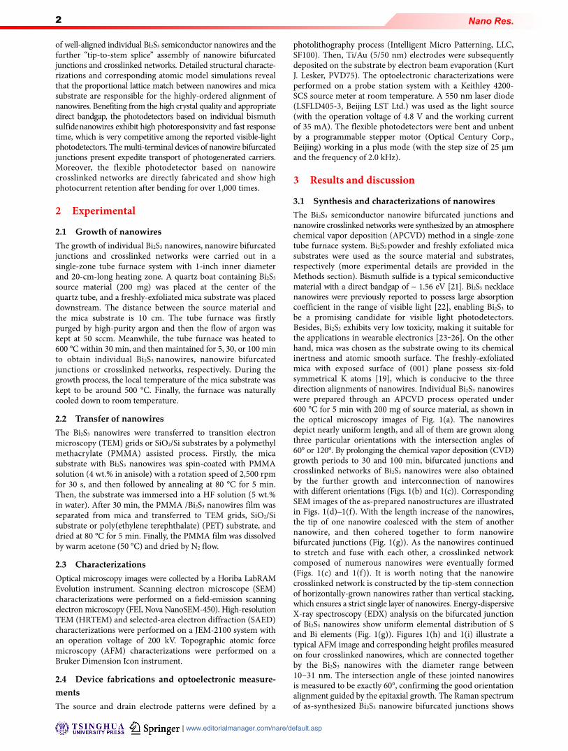
Figure 6 Photoresponse of a flexible photodetector based on Bi2S3 nanowire crosslinked network. (a) Scheme diagram and digital photograph of the flexible photodetector. (b) I–V curves measured from the flexible photo-detector under dark and different illumination intensities. The wavelength of incident light is 550 nm. (c) Photocurrent (Iph) as a function of illumination intensity (P) under a bias of 15 V. (d) Time-resolved photoresponse of the flexible photodetector with a period of 4 s under a bias of 10 V, showing fast photoresponse (tr = 33 ms and td = 50 ms). (e) I–V curves of the flexible photodetector before and after bending for 500 and 1,000 times. (f) The change of photocurrent (Iph) after different bending times.
bending test has negligible effect on the performance of flexible photodetectors. The time-dependent photoresponse curves (Fig. 6(d)) exhibit reversible photoresponse with a raise time of 33 ms and a decay time of 50 ms (Figs. S3(c) and S3(d) in the ESM), which are both slightly faster than the response times of individual nanowire photodetector (Fig. 4(d)). To evaluate the flexibility of the bendable photoreactor, the device on mica substrate was bent for different times by a programmable stepper motor, as illustrated in the inset of Fig. 6(f). The bending parameters can be described by α, R and L, which are corresponding to the bending angle, bending radius and the length of the device, respectively [38]. In our experiment, the values of α, R and L are fixed at 90°, 3 and 25 mm during each bending cycle, respectively. After bending for 500 and 1,000 times, the photocurrent of the device presents the retention ratios of 95% and 87% (Figs. 6(e) and 6(f)), indicating the good flexibility and stability of the crosslinked nanowire network. The high crystalline quality of the crosslinked Bi2S3 nanowire network is responsible for the outstanding photoresponse performance of the bendable photodetectors.
4 Conclusion In summary, we report an effective lattice-matching strategy to achieve the growth of regularly-oriented individual Bi2S3 semiconductor nanowires, as well as bifurcated junctions and crosslinked networks. Through atomic structure analysis and modeling, a “tip-to-stem splice” mechanism is proposed to elucidate the aligned connection and assembly of nanowire
bifurcated junctions and crosslinked networks. Detailed characterizations reveal that the nanowires exhibit high crystalline quality and low impedance between the junction interfaces. The photodetectors based on individual Bi2S3 nanowires exhibit remarkable photoresponsivity and fast switch time under visible light, which is very competitive among the existing nanowire-based photodetectors. The optoelectronic measure-ments of three-terminal devices based on nanowire bifurcated junctions also depict effective carrier transport across the junctions. Benefiting from the flexible and interconnected features, the photodetectors based on nanowire crosslinked networks present high stability during long-term bending tests. Our findings present new directions for the controlled growth of regularly-assembled low-dimensional nanostructures for nanoelectronic devices.
Acknowledgements
Author Contributions
Z. J. and Y. H. conceived the idea of this study and designed the experiments. Y. H. performed the sample synthesis, AFM characterizations and device measurements. L. Y. M., X. Y., J. Y. L., R. P. C., T. C., W. J. Z., X. L. X. and W. Y. performed the material characterizations. X. L. Z. and M. S. helped the data analysis. Y. H. and Z. J. co-wrote and revised the manuscript. All the authors discussed the results. Z. J. supervised this research project.
Funding Sources
This work was supported by the National Key R&D Program (Nos. 2017YFA0208200 and 2016YFB0700600), the Fundamental Research Funds for the Central Universities (No. 0205-14380219), the Projects of the National Natural Science Foundation of China (NSFC) (Nos. 21872069, 51761135104, and 21573108), the Natural Science Foundation of Jiangsu Province (No. BK20180008), and the High-Level Innovation and Entrepreneurship Project of Jiangsu Province of China.
Electronic Supplementary Material: Supplementary material (HRTEM images, output and transfer characteristic curves, zoom-in images of the rise and decay regions, and I–V curves) is available in the online version of this article at https://doi.org/10.1007/s12274-020-2841-6.
References [1] Lu, W.; Lieber, C. M. Nanoelectronics from the bottom up. Nat.
Mater. 2007, 6, 841–850. [2] Zhai, T. Y.; Li, L.; Wang, X.; Fang, X. S.; Bando, Y.; Golberg, D.
Recent developments in one-dimensional inorganic nanostructures for photodetectors. Adv. Funct. Mater. 2010, 20, 4233–4248.
[3] Yan, R. X.; Gargas, D.; Yang, P. D. Nanowire photonics. Nat. Photonics 2009, 3, 569–576.
[4] Yan, R. X.; Park, J. H.; Choi, Y.; Heo, C. J.; Yang, S. M.; Lee, L. P.; Yang, P. D. Nanowire-based single-cell endoscopy. Nat. Nanotechnol. 2012, 7, 191–196.
[5] Long, Y. Z.; Yu, M.; Sun, B.; Gu, C. Z.; Fan, Z. Y. Recent advances in large-scale assembly of semiconducting inorganic nanowires and nanofibers for electronics, sensors and photovoltaics. Chem. Soc. Rev. 2012, 41, 4560–4580.
[6] Huang, Y.; Duan, X. F.; Wei, Q. Q.; Lieber, C. M. Directed assembly of one-dimensional nanostructures into functional networks. Science 2001, 291, 630–633.
[7] Wang, D. L.; Qian, F.; Yang, C.; Zhong, Z. H.; Lieber, C. M. Rational growth of branched and hyperbranched nanowire structures. Nano Lett. 2004, 4, 871–874.
[8] Manna, L.; Milliron, D. J.; Meisel, A.; Scher, E. C.; Alivisatos, A. P.

Nano Res.
www.theNanoResearch.com∣www.Springer.com/journal/12274 | Nano Research
7
Controlled growth of tetrapod-branched inorganic nanocrystals. Nat. Mater. 2003, 2, 382–385.
[9] Jiang, X. C.; Tian, B. Z.; Xiang, J.; Qian, F.; Zheng, G. F.; Wang, H. T.; Mai, L. Q.; Lieber, C. M. Rational growth of branched nanowire heterostructures with synthetically encoded properties and function. Proc. Natl. Acad. Sci. USA 2011, 108, 12212–12216.
[10] Huang, Y.; Duan, X. F.; Cui, Y.; Lauhon, L. J.; Kim, K. H.; Lieber, C. M. Logic gates and computation from assembled nanowire building blocks. Science 2001, 294, 1313–1317.
[11] Zhong, Z. H.; Wang, D. L.; Cui, Y.; Bockrath, M. W.; Lieber, C. M. Nanowire crossbar arrays as address decoders for integrated nanosystems. Science 2003, 302, 1377–1379.
[12] Baca, A. J.; Ahn, J. H.; Sun, Y. G.; Meitl, M. A.; Menard, E.; Kim, H. S.; Choi, W. M.; Kim, D. H.; Huang, Y.; Rogers, J. A. Semiconductor wires and ribbons for high-performance flexible electronics. Angew. Chem., Int. Ed. 2008, 47, 5524–5542.
[13] Liu, X.; Long, Y. Z.; Liao, L.; Duan, X. F.; Fan, Z. Y. Large-scale integration of semiconductor nanowires for high-performance flexible electronics. ACS Nano 2012, 6, 1888–1900.
[14] Melosh, N. A.; Boukai, A.; Diana, F.; Gerardot, B.; Badolato, A.; Petroff, P. M.; Heath, J. R. Ultrahigh-density nanowire lattices and circuits. Science 2003, 300, 112–115.
[15] Plissard, S. R.; van Weperen, I.; Car, D.; Verheijen, M. A.; Immink, G. W. G.; Kammhuber, J.; Cornelissen, L. J.; Szombati, D. B.; Geresdi, A.; Frolov, S. M. et al. Formation and electronic properties of InSb nanocrosses. Nat. Nanotechnol. 2013, 8, 859–864.
[16] Rieger, T.; Rosenbach, D.; Vakulov, D.; Heedt, S.; Scha ̈pers, T.; Gru ̈tzmacher, D.; Lepsa, M. I. Crystal phase transformation in self-assembled InAs nanowire junctions on patterned Si substrates. Nano Lett. 2013, 16, 1933–1941.
[17] Yao, Y. G.; Fu, K. K.; Zhu, S. Z.; Dai, J. Q.; Wang, Y. B.; Pastel, G.; Chen, Y. N.; Li, T.; Wang, C. W.; Li, T. et al. Carbon welding by ultrafast joule heating. Nano Lett. 2016, 16, 7282–7289.
[18] Tsivion, D.; Schvartzman, M.; Popovitz-Biro, R.; von Huth, P.; Joselevich, E. Guided growth of millimeter-long horizontal nanowires with controlled orientations. Science 2011, 333, 1003–1007.
[19] Peng, H. L.; Dang, W. H.; Cao, J.; Chen, Y. L.; Wu, D.; Zheng, W. S.; Li, H.; Shen, Z. X.; Liu, Z. F. Topological insulator nanostructures for near- infrared transparent flexible electrodes. Nat. Chem. 2012, 4, S–286.
[20] Wang, Q. S.; Li, J.; Lei, Y.; Wen, Y.; Wang, Z. X.; Zhan, X. Y.; Wang, F.; Wang, F. M.; Huang, Y.; Xu, K. et al. Oriented growth of Pb1−xSnxTe nanowire arrays for integration of flexible infrared detectors. Adv. Mater. 2016, 28, 3596–3601.
[21] Peng, X. S.; Meng, G. W.; Zhang, J.; Zhao, L. X.; Wang, X. F.; Wang, Y. W.; Zhang, L. D. Electrochemical fabrication of ordered Bi2S3 nanowire arrays. J. Phys. D Appl. Phys. 2001, 34, 3224–3228.
[22] Cademartiri, L.; Malakooti, R.; O'Brien, P. G.; Migliori, A.; Petrov, S.; Kherani, N. P.; Ozin, G. A. Innentitelbild: Large-scale synthesis of ultrathin Bi2S3 necklace nanowires. Angew. Chem. 2008, 120, 3708.
[23] Biswas, K.; Zhao, L. D.; Kanatzidis, M. G. Tellurium-free thermoelectric: The anisotropic n-type semiconductor Bi2S3. Adv. Energy Mater.
2012, 2, 634–638. [24] Mohan, R. Green bismuth. Nat. Chem. 2010, 2, 336. [25] Thomson, J. W.; Cademartiri, L.; MacDonald, M.; Petrov, S.; Calestani,
G.; Zhang, P.; Ozin, G. A. Ultrathin Bi2S3 nanowires: Surface and core structure at the cluster-nanocrystal transition. J. Am. Chem. Soc. 2010, 132, 9058–9068.
[26] Cademartiri, L.; Scotognella, F.; O’Brien, P. G.; Lotsch, B. V.; Thomson, J.; Petrov, S.; Kherani, N. P.; Ozin, G. A. Cross-linking Bi2S3 ultrathin nanowires: A platform for nanostructure formation and biomolecule detection. Nano Lett. 2009, 9, 1482–1486.
[27] Li, Y. T.; Huang, L.; Li, B.; Wang, X. T.; Zhou, Z. Q.; Li, J. B.; Wei, Z. M. Co-nucleus 1D/2D heterostructures with Bi2S3 nanowire and MoS2 monolayer: One-step growth and defect-induced formation mechanism. ACS Nano 2016, 10, 8938–8946.
[28] Tang, C. J.; Wang, C. Q.; Su, F. J.; Zang, C. H.; Yang, Y. X.; Zong, Z. J.; Zhang, Y. S. Controlled synthesis of urchin-like Bi2S3 via hydrothermal method. Solid State Sci. 2010, 12, 1352–1356.
[29] Lopez-Sanchez, O.; Lembke, D.; Kayci, M.; Radenovic, A.; Kis, A. Ultrasensitive photodetectors based on monolayer MoS2. Nat. Nanotechnol. 2013, 8, 497–501.
[30] Xu J. Z.; Li, H. N.; Fang, S. F.; Jiang, K.; Yao, H. Z.; Fang, F. E.; Chen, F. M.; Wang, Y.; Shi, Y. M. Synthesis of bismuth sulfide nanobelts for high performance broadband photodetectors. J. Mater. Chem. C 2020, 8, 2102–2108.
[31] Chao, J. F.; Xing, S. M.; Liu, Z. D.; Zhang, X. T.; Zhao, Y. L.; Zhao, L. H.; Fan, Q. F. Large-scale synthesis of Bi2S3 nanorods and nanoflowers for flexible near-infrared laser detectors and visible light photodetectors. Mater. Res. Bull. 2018, 98, 194–199.
[32] Chen, G. H.; Yu, Y. Q.; Zheng, K.; Ding, T.; Wang, W. L.; Jiang, Y.; Yang, Q. Fabrication of ultrathin Bi2S3 nanosheets for high-performance, flexible, visible-NIR photodetectors. Small 2015, 11, 2848–2855.
[33] Xiao, G. J.; Dong, Q. F.; Wang, Y. N.; Sui, Y. M.; Ning, J. J.; Liu, Z. Y.; Tian, W. J.; Liu, B. B.; Zou G. T.; Zou, B. One-step solution synthesis of bismuth sulfide (Bi2S3) with various hierarchical architectures and their photoresponse properties. RSC Adv. 2012, 2, 234–240.
[34] Konstantatos, G.; Levina, L.; Tang, J.; Sargent H. E. Sensitive solution-processed Bi2S3 nanocrystalline photodetectors. Nano Lett. 2008, 8, 4002–4006.
[35] Zhai, T. Y.; Li, L.; Ma, Y.; Liao, M. Y.; Wang, X.; Fang, X. S.; Yao, J. N.; Bando, Y.; Golberg, D. One-dimensional inorganic nanostructures: Synthesis, field-emission and photodetection. Chem. Soc. Rev. 2011, 40, 2986–3004.
[36] Soci, C.; Zhang, A.; Xiang, B.; Dayeh, S. A.; Aplin, D. P. R.; Park, J.; Bao, X. Y.; Lo, Y. H.; Wang, D. ZnO nanowire UV photodetectors with high internal gain. Nano Lett. 2007, 7, 1003–1009.
[37] Li, Q. L.; Li, Y.; Gao, J.; Wang, S. D.; Sun, X. H. High performance single In2Se3 nanowire photodetector. Appl. Phys. Lett. 2011, 99, 243105.
[38] Li, H. F.; Tang, Z. J.; Liu, Z. X.; Zhi, C. Y. Evaluating flexibility and wearability of flexible energy storage devices. Joule 2019, 3, 613–619.


![Bio‐Based Transparent Conductive Film Consisting of ...homepage.ntu.edu.tw/~shtung/Publications/2018_Macromol...flexible optoelectronic devices.[1] Among which, PET, as the most](https://static.fdocuments.in/doc/165x107/613cd4514c23507cb635a1a1/bioabased-transparent-conductive-film-consisting-of-shtungpublications2018macromol.jpg)
![Controllable Sliding Bearings and Controllable Lubrication ... · Review Controllable Sliding Bearings and Controllable ... or evolutionary [5], but it does not change the fact that](https://static.fdocuments.in/doc/165x107/5fc50df11ca4e1756528a85b/controllable-sliding-bearings-and-controllable-lubrication-review-controllable.jpg)