Concept Creation and Design of a Parameterizable, fast...
34
Concept Creation and Design of a Parameterizable, fast-locking 65 nm CMOS CDR-PLL for Gigabit Serial Chip-to-Chip Communication in Mobile Devices Milan Forcan by Prof. Dr.-Ing. Klaus Solbach University of Duisburg-Essen Department of Microwave and RF-Technology Prof. Dr.-Ing. Werner Schardein University of Applied Sciences Dortmund Markus Müller Nokia Research Center Bochum Reimund Wittmann Ralf Kakerow
-
Upload
hoangquynh -
Category
Documents
-
view
217 -
download
0
Transcript of Concept Creation and Design of a Parameterizable, fast...

Concept Creation and Design of a Parameterizable, fast-locking 65 nm CMOS
CDR-PLL for Gigabit Serial Chip-to-Chip Communication in
Mobile Devices
Milan Forcan
by
Prof. Dr.-Ing. Klaus SolbachUniversity of Duisburg-Essen
Department of Microwave and RF-Technology
Prof. Dr.-Ing. Werner SchardeinUniversity of Applied Sciences Dortmund
Markus MüllerNokia Research Center Bochum
Reimund Wittmann Ralf Kakerow

Contents• Introduction
• Clock and Data Recovery Architectures
• Clock and Data Recovery PLL
• Oversampling CDR
• Analysis of Clock and Data Recovery Circuits
• Simulation Environment
• Hogge PD vs. Alexander PD
• CDR-PLL Implementation
• Generic Engineering Model
• CDR-PLL Building Blocks

• Basic structure of a serial data link:
• Serial data transmission with embedded clock
• How to determine which bit is sent?
• Solution: Clock and Data Recovery Circuit– Extract the clock signal and align it to data– Resample the noisy analog data signal
• Challenges: – Extremely fast locking time compared to conservative CDR– Sufficient jitter performance
Introduction

Contents• Introduction
• Clock and Data Recovery Architectures
• Clock and Data Recovery PLL
• Oversampling CDR
• Analysis of Clock and Data Recovery Circuits
• Simulation Environment
• Hogge PD vs. Alexander PD
• CDR-PLL Implementation
• Generic Engineering Model
• CDR-PLL Building Blocks
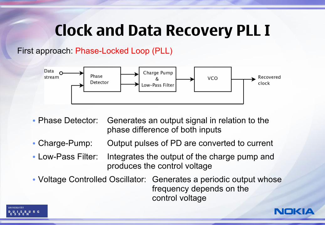
Clock and Data Recovery PLL IFirst approach: Phase-Locked Loop (PLL)
• Phase Detector: Generates an output signal in relation to thephase difference of both inputs
• Charge-Pump: Output pulses of PD are converted to current
• Low-Pass Filter: Integrates the output of the charge pump and produces the control voltage
• Voltage Controlled Oscillator: Generates a periodic output whosefrequency depends on the control voltage

Hogge Phase Detector (Linear PD):
• Path Y produces proportional pulses in relation to phase difference
• Path X produces Tck
/2 wide reference pulses
• Under locked condition Y & X show pulses with equal width
Clock and Data Recovery PLL II

Hogge Phase Detector (Linear PD):
• Benefits:
• Linear dependence between output andphase difference
• Wide frequency acquisition range
• Linear behaviour enables loop parameters calculation
• Drawback:
• “Triwaves” are produced, resulting in noise on oscillator line
• Clock skew due to internal delays
Clock and Data Recovery PLL III

Alexander Phase Detector (Bang-Bang PD):
• Data is sampled at 3 equidistant points A, B and C
• XOR gates combine nodes A, B ad C:
X = A xor B and Y = B xor C
• Performs an early-late detection
Clock is early: Y = Low and X = High
Clock is late: Y = High and X = Low
Clock and Data Recovery PLL IV

Alexander Phase Detector (Bang-Bang PD):
• Benefit:
• In steady state clock is aligned in the middleof the data eye
• Drawback:
• Small frequency capture range
Clock and Data Recovery PLL V

Contents• Introduction
• Clock and Data Recovery Architectures
• Clock and Data Recovery PLL
• Oversampling CDR
• Analysis of Clock and Data Recovery Circuits
• Simulation Environment
• Hogge PD vs. Alexander PD
• CDR-PLL Implementation
• Generic Engineering Model
• CDR-PLL Building Blocks

Second approach: Oversampling CDR
1. Sample data at equidistant points
2. Detect data transition occurrence
3. Select clock phase to resample the data
Benefits:
Digital implementation
Very fast acquisition
Drawbacks:
Design complexity increases with frequency and jitter requirements
Additional multiphase VCO/PLL needed
Oversampling CDR

Contents• Introduction
• Clock and Data Recovery Architectures
• Clock and Data Recovery PLL
• Oversampling CDR
• Analysis of Clock and Data Recovery Circuits
• Simulation Environment
• Hogge PD vs. Alexander PD
• CDR-PLL Implementation
• Generator Driven Generic Engineering Model
• CDR-PLL Building Blocks

• Implementation of appropriate models for first comparison ofHogge PD and Alexander PD
• SKILL code generates data stream:
• 1.25 Gb/s (1UI = 800ps)
• Pseudo-random
• Adjustable Jitter
• 8B10B-coding
• Verilog-A models:
• Charge-Pump
• Voltage Controlled Oscillator
Simulation Environment

• Implementation of appropriate models for first comparison ofHogge PD and Alexander PD
• SKILL code generates data stream:
• 1.25 Gb/s (1UI = 800ps)
• Pseudo-random
• Adjustable Jitter
• 8B10B-coding
• Verilog-A models:
• Charge-Pump
• Voltage Controlled Oscillator
Simulation Environment

Hogge PD simulation results:• Pro:
• Wide frequencyacquisition range
• Linear behaviour
• Fast locking time of500 ns (625 UI)
• Contra:
• Triwaves on theoscillator line
• Systematic clock skew of150 ps (0.18 UI)
Hogge PD vs. Alexander PD I
Trainingsequence
Datasequence

Hogge PD simulation results:• Pro:
• Wide frequencyacquisition range
• Linear behaviour
• Fast locking time of500 ns (625 UI)
• Contra:
• Triwaves on theoscillator line
• Systematic clock skew of 150 ps (0.18 UI)
Hogge PD vs. Alexander PD I
Trainingsequence
Datasequence

Alexander PD simulation results:• Pro:
• Successful phase lock
• Contra:
• Higher noise onoscillator line
• Frequency acquisition range < 100 MHz!
• Additional frequencydetection required
Hogge PD vs. Alexander PD II
Trainingsequence
Datasequence

● Hogge PD:
● Wide frequency acquisition range
● Fast acquisition time
● Acceptable output clock jitter
● Triwaves and clock skew
● Alexander PD:
● Successful lock
● Narrow frequency acquisition range requires frequency detection
● Oversampling CDR approach:
● Very fast acquisition time
● High design efforts
● More than 6 phases required for reasonable jitter performance
Circuit Selection
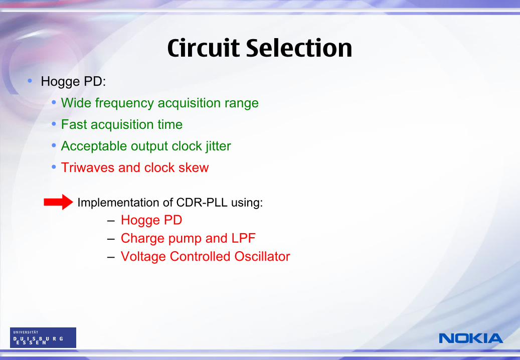
● Hogge PD:
● Wide frequency acquisition range
● Fast acquisition time
● Acceptable output clock jitter
● Triwaves and clock skew
Implementation of CDR-PLL using:
– Hogge PD– Charge pump and LPF– Voltage Controlled Oscillator
Circuit Selection

Contents• Introduction
• Clock and Data Recovery Architectures
• Clock and Data Recovery PLL
• Oversampling CDR
• Analysis of Clock and Data Recovery Circuits
• Simulation Environment
• Hogge PD vs. Alexander PD
• CDR-PLL Implementation
• Generic Engineering Model
• CDR-PLL Building Blocks

• C-like description generates schematic, layout and testbench
• Variables define technology dependent design rules
• Create instances, wires and contacts using functions
• Benefits:
• Reusable circuit generators
• Generator parametersallow fast modification ofimplemented circuit
• Technology independent
• Adaptable on common CAD systems(e.g. Mentor, Cadence)
Generic Engineering Model (GEM)
VariablesTechnologydependent
GeneratorTechnologyindependent
GEMGEMEnvironmentEnvironment
CELLSSchematic
SymbolLayout
CA
D E
nviro
nmen
t

Modifications on Hogge PD:
• Correct clock skew using first delay
• Eliminate Triwaves using second delay
Modifications on LPF:
• Capacitances C1 = 100 fFC2 = 1.9 pF
• Resistor R1 = 8.3 kOhms
• Loop transfer function:
• Bandwidth f0dB = 50.5 MHz
• Phase margin PM = 65 °
• Overshoot = 1.29 dB
CDR-PLL Building Blocks I

• Current-Starved Voltage Controlled Oscillator:
CDR-PLL Building Blocks II

• VCO specifications:
• Operating point: 1.25 GHz at 0.65V
• Limited linear range
• Tuning range:1.17 GHz – 1.42 GHz
• VCO slope: 400 MHz/V
• Parameter verification with layout simulation required
CDR-PLL Building Blocks III• VCO frequency characteristic:

• Current steering Charge Pump:
CDR-PLL Building Blocks IV
n-MOS switches
p-MOS switches
p-MOS source
n-MOS source

• Charge pump DC characteristic:
CDR-PLL Building Blocks V• Charge pump specifications:
• Suitable for high speeds
• Scalable currents
• Limited linear range
• 100 μA at operating point

• Locking time: 55 ns ≈ 70 UI(up to 10x faster than conservative CDR-PLL)
• Input jitter tolerance: 0.39 UI at 1.25 GB/s verified(SATA compliant)
• Clock output jitter: 0.26 UI at 0.39 UI data jitter
• Power consumption: 0.615 mW at 1V
• CDR core dimensions: 100 μm x 100 μm
Simulation Results

Thank you for your attention!

• VCO layout
Appendix

• Charge pump layout
Appendix

Appendix• Oversampling CDR
(input stage):• Oversampling CDR
(transition detection):

Appendix• Oversampling CDR
(USEA signal stage):• Oversampling CDR
(USEC signal stage):

Appendix• Oversampling CDR
(SELA signal stage):• Oversampling CDR
(phase switching stage):