
Cold Electronics for Very Large LAr TPCs - Fermilab
21
1 Cold Electronics for Very Large LAr TPCs Veljko Radeka BNL for “Cold Electronics Team”: Gianluigi De Geronimo, Sergio Rescia, Hucheng Chen BNL Grzegorz Deptuch, Ray Yarema FNAL LAr20 Review, Nov 23, 2009
Transcript of Cold Electronics for Very Large LAr TPCs - Fermilab
11
Cold Electronics for Very Large LAr TPCs
Veljko RadekaBNLfor
“Cold Electronics Team”:
Gianluigi De Geronimo, Sergio Rescia, Hucheng ChenBNL
Grzegorz Deptuch, Ray YaremaFNAL
LAr20 Review, Nov 23, 2009
2
Outlne:
•TPC Signals: 3-6•Noise: 7-9•“Cold” vs “Warm” electronics: 10-12•Readout chain concept: 13-17•Reliability of CMOS: 18-19•R&D plan 20-21
Slides:
333
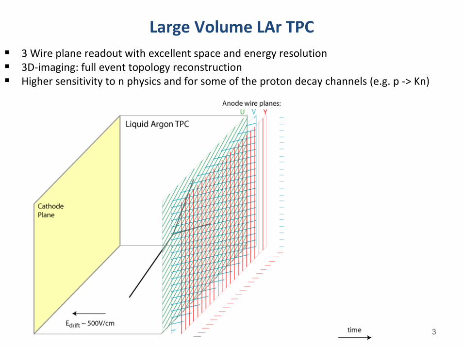
Large Volume LAr TPC3 Wire plane readout with excellent space and energy resolution3D‐imaging: full event topology reconstructionHigher sensitivity to n physics and for some of the proton decay channels (e.g. p ‐> Kn)
444
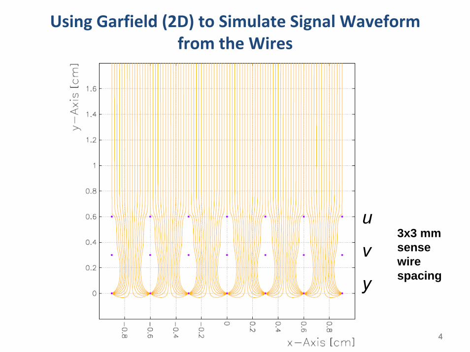
Using Garfield (2D) to Simulate Signal Waveform from the Wires
u
v
y
3x3 mm sense wire spacing
55
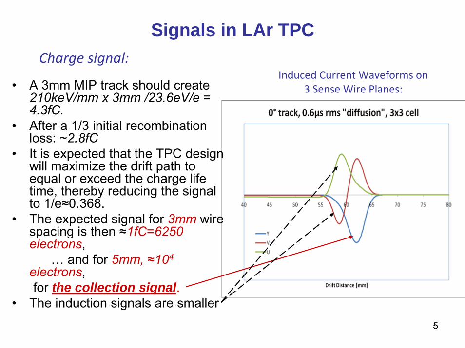
Signals in LAr TPC
• A 3mm MIP track should create 210keV/mm x 3mm /23.6eV/e = 4.3fC.
• After a 1/3 initial recombination loss: ~2.8fC
• It is expected that the TPC design will maximize the drift path to equal or exceed the charge life time, thereby reducing the signal to 1/e≈0.368.
• The expected signal for 3mm wire spacing is then ≈1fC=6250 electrons,
… and for 5mm, ≈104
electrons,for the collection signal.
• The induction signals are smaller
Induced Current Waveforms on 3 Sense Wire Planes:
Charge signal:
66
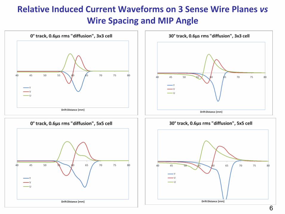
Relative Induced Current Waveforms on 3 Sense Wire Planes vsWire Spacing and MIP Angle
6
77
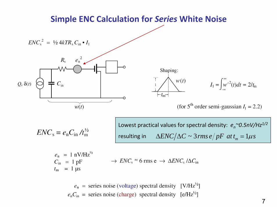
Simple ENC Calculation for SeriesWhite Noise
7
Lowest practical values for spectral density: en~0.5nV/Hz1/2
resulting in ~ 3 1mENC C rms e pF at t sμΔ Δ =
88
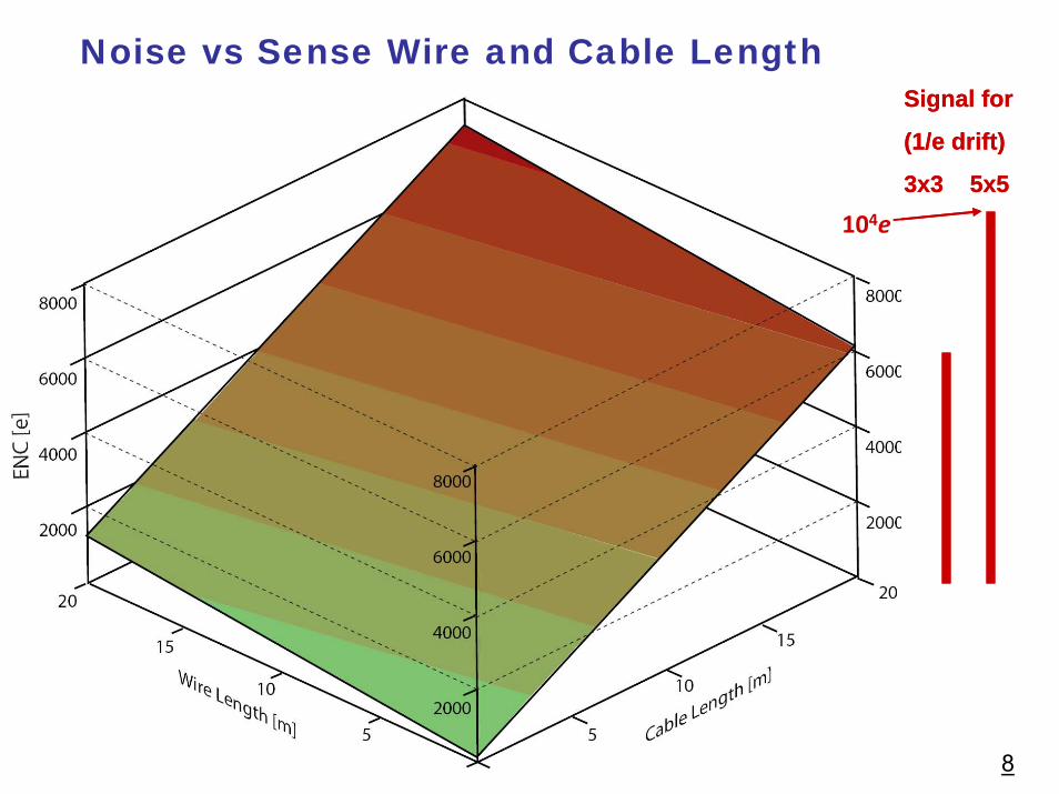
Signal for
(1/e drift)
3x3 5x5104e
Signal for
(1/e drift)
3x3 5x5104e
Noise vs Sense Wire and Cable Length
8
99
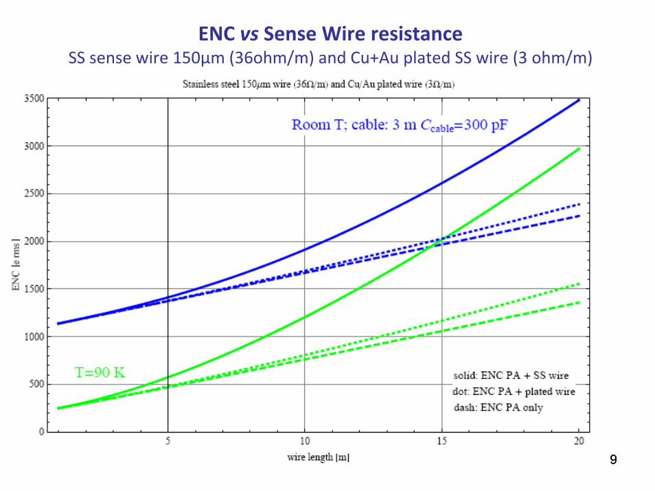
ENC vs Sense Wire resistanceSS sense wire 150µm (36ohm/m) and Cu+Au plated SS wire (3 ohm/m)
1010
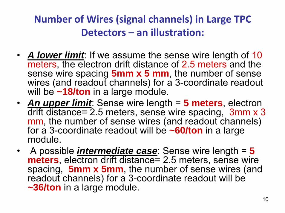
Number of Wires (signal channels) in Large TPC Detectors – an illustration:
• A lower limit: If we assume the sense wire length of 10 meters, the electron drift distance of 2.5 meters and the sense wire spacing 5mm x 5 mm, the number of sense wires (and readout channels) for a 3-coordinate readout will be ~18/ton in a large module.
• An upper limit: Sense wire length = 5 meters, electron drift distance= 2.5 meters, sense wire spacing, 3mm x 3 mm, the number of sense wires (and readout channels) for a 3-coordinate readout will be ~60/ton in a large module.
• A possible intermediate case: Sense wire length = 5 meters, electron drift distance= 2.5 meters, sense wire spacing, 5mm x 5mm, the number of sense wires (and readout channels) for a 3-coordinate readout will be ~36/ton in a large module.
1111
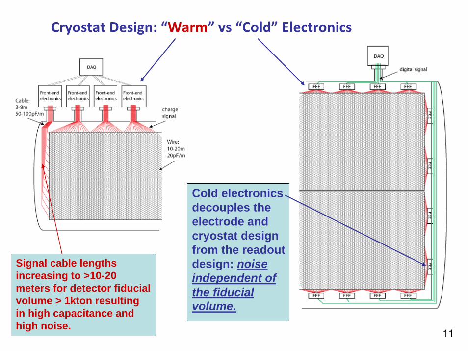
Signal cable lengths increasing to >10-20 meters for detector fiducialvolume > 1kton resulting in high capacitance and high noise.
Cold electronics decouples the electrode and cryostat design from the readout design: noise independent of the fiducialvolume.
Cryostat Design: “Warm” vs “Cold” Electronics
11
1212
“Cold” vs “Warm” Summary:
• For detector fiducial volume > 1kton signal cable lengths of >10-20 meters will be required due to the cryostat size to bring thesignals from the sense wires to the feedthroughs (and externalwarm electronics) resulting in high capacitance and high noise. (The feedthroughs will have to be located on top of the cryostat to minimize the heat input and to simplify the construction of the cryostat.)
• Cold electronics will make possible to decouple the electrode and cryostat design from the readout design (no limit on the cable length within the cryostat after the signals are amplifiedand digitized at the sense wires, so that the noise will be independent of the fiducial volume and much lower than with the warm electronics.
• Signal multiplexing within the cryostat will result in a large reduction in the quantity of cables (less outgassing) and the number of feedthroughs/penetrations (lower cost and probability of leaks).
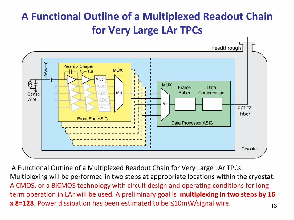
1313
A Functional Outline of a Multiplexed Readout Chain for Very Large LAr TPCs. Multiplexing will be performed in two steps at appropriate locations within the cryostat. A CMOS, or a BiCMOS technology with circuit design and operating conditions for long term operation in LAr will be used. A preliminary goal is multiplexing in two steps by 16 x 8=128. Power dissipation has been estimated to be ≤10mW/signal wire.
A Functional Outline of a Multiplexed Readout Chain for Very Large LAr TPCs
14
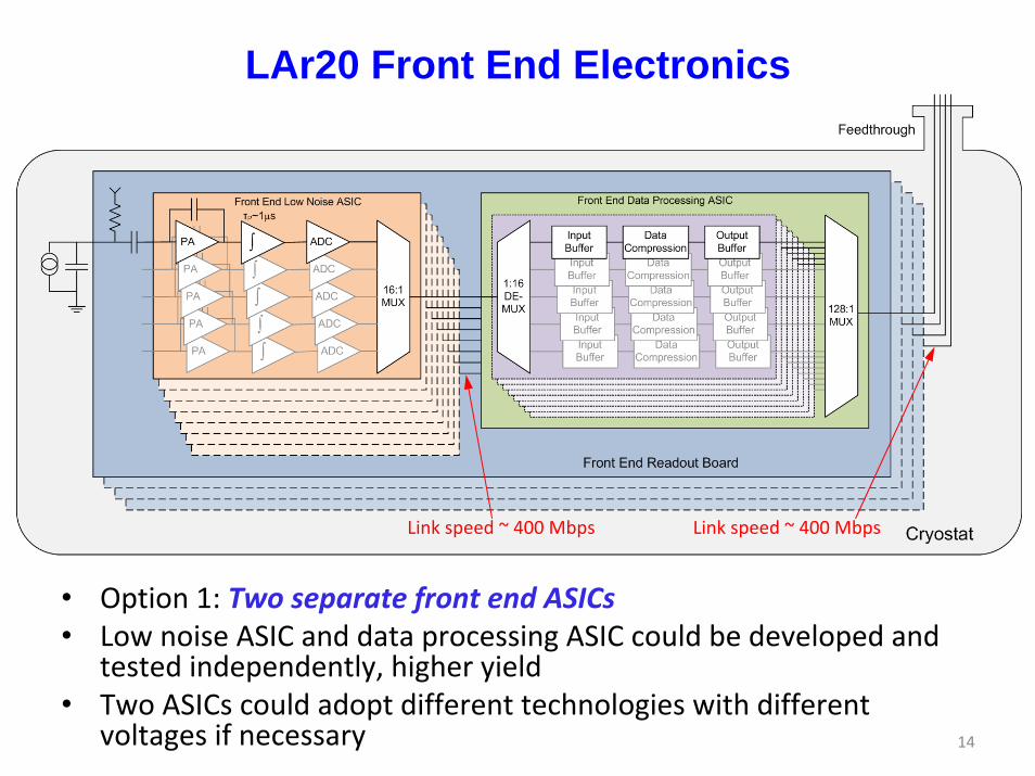
LAr20 Front End Electronics
• Option 1: Two separate front end ASICs• Low noise ASIC and data processing ASIC could be developed and
tested independently, higher yield • Two ASICs could adopt different technologies with different
voltages if necessary
Link speed ~ 400 Mbps Link speed ~ 400 Mbps
15
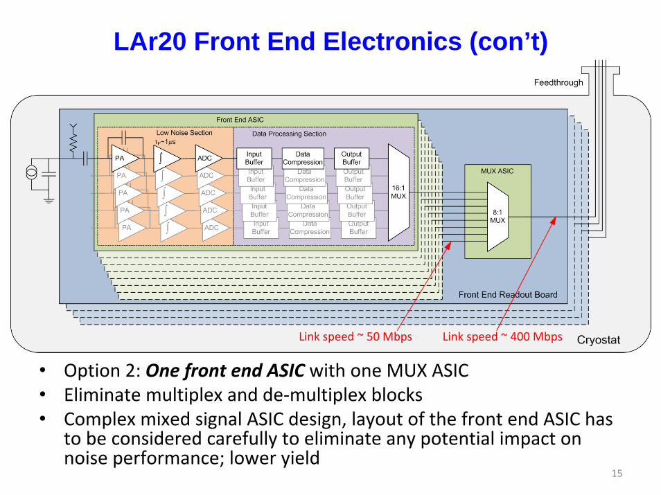
LAr20 Front End Electronics (con’t)
• Option 2: One front end ASIC with one MUX ASIC• Eliminate multiplex and de‐multiplex blocks • Complex mixed signal ASIC design, layout of the front end ASIC has
to be considered carefully to eliminate any potential impact on noise performance; lower yield
Link speed ~ 50 Mbps Link speed ~ 400 Mbps
16
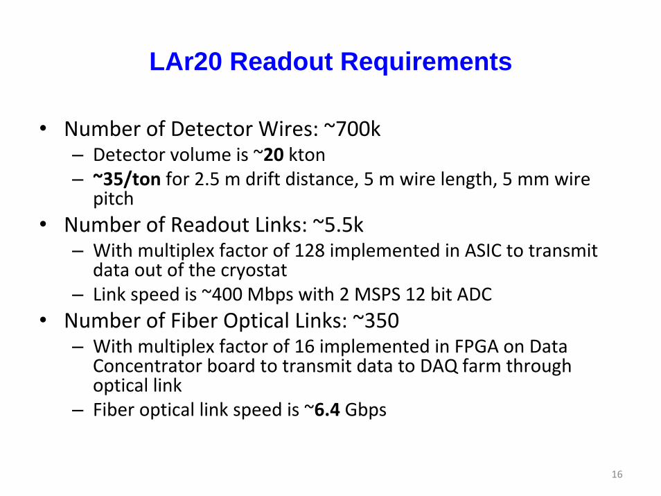
LAr20 Readout Requirements
• Number of Detector Wires: ~700k – Detector volume is ~20 kton– ~35/ton for 2.5 m drift distance, 5 m wire length, 5 mm wire
pitch• Number of Readout Links: ~5.5k
– With multiplex factor of 128 implemented in ASIC to transmit data out of the cryostat
– Link speed is ~400 Mbps with 2 MSPS 12 bit ADC• Number of Fiber Optical Links: ~350
– With multiplex factor of 16 implemented in FPGA on Data Concentrator board to transmit data to DAQ farm through optical link
– Fiber optical link speed is ~6.4 Gbps
17
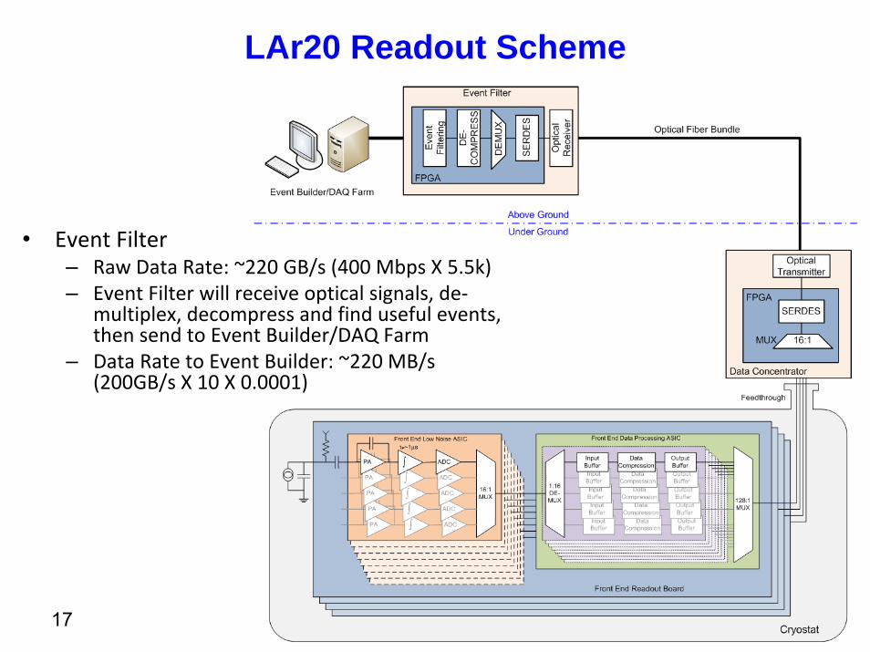
LAr20 Readout Scheme
• Event Filter– Raw Data Rate: ~220 GB/s (400 Mbps X 5.5k)– Event Filter will receive optical signals, de‐
multiplex, decompress and find useful events, then send to Event Builder/DAQ Farm
– Data Rate to Event Builder: ~220 MB/s (200GB/s X 10 X 0.0001)
17
18
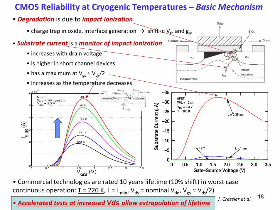
• Degradation is due to impact ionization
• charge trap in oxide, interface generation → shift in Vth and gm
• Substrate current is a monitor of impact ionization• increases with drain voltage
• is higher in short channel devices
• has a maximum at Vgs ≈ Vds/2
• increases as the temperature decreases
CMOS Reliability at Cryogenic Temperatures – Basic Mechanism
• Commercial technologies are rated 10 years lifetime (10% shift) in worst case continuous operation: T = 220 K, L = Lmin, Vds = nominal Vdd, Vgs ≈ Vds/2)
• Accelerated tests at increased Vds allow extrapolation of lifetimeJ. Cressler et al.
19
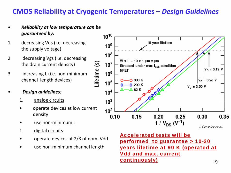
• Reliability at low temperature can be guaranteed by:
1. decreasing Vds (i.e. decreasing the supply voltage)
2. decreasing Vgs (i.e. decreasing the drain current density)
3. increasing L (i.e. non‐minimum channel length devices)
• Design guidelines:
1. analog circuits
• operate devices at low current density
• use non‐minimum L
1. digital circuits
• operate devices at 2/3 of nom. Vdd
• use non‐minimum channel length
J. Cressler et al.
Accelerated tests will be
CMOS Reliability at Cryogenic Temperatures – Design Guidelines
performed to guarantee > 10-20 years lifetime at 90 K (operated at Vdd and max. current continuously)
20
Collaboration with Georgia Tech on Cryogenic Electronics
• Strong group led by J. Cressler, with experience in “extreme environment” electronics (development for NASA of electronics for the Lunar Base Station project).
• Expertise in cryogenic CMOS and BiCMOS (SiGe HBJT), Cresslerwas a key person in developing SiGe process at IBM.
• Cressler has agreed to collaborate with BNL/FNAL in development of cryogenic electronics for LBNE.
• Topics:
1. Process and device reliability qualifications2. Device testing at cryogenic temperature3. Device modeling at cryogenic temperature4. Development of circuit blocks needed in the system (e.g.
bandgap reference, voltage regulator).
2121
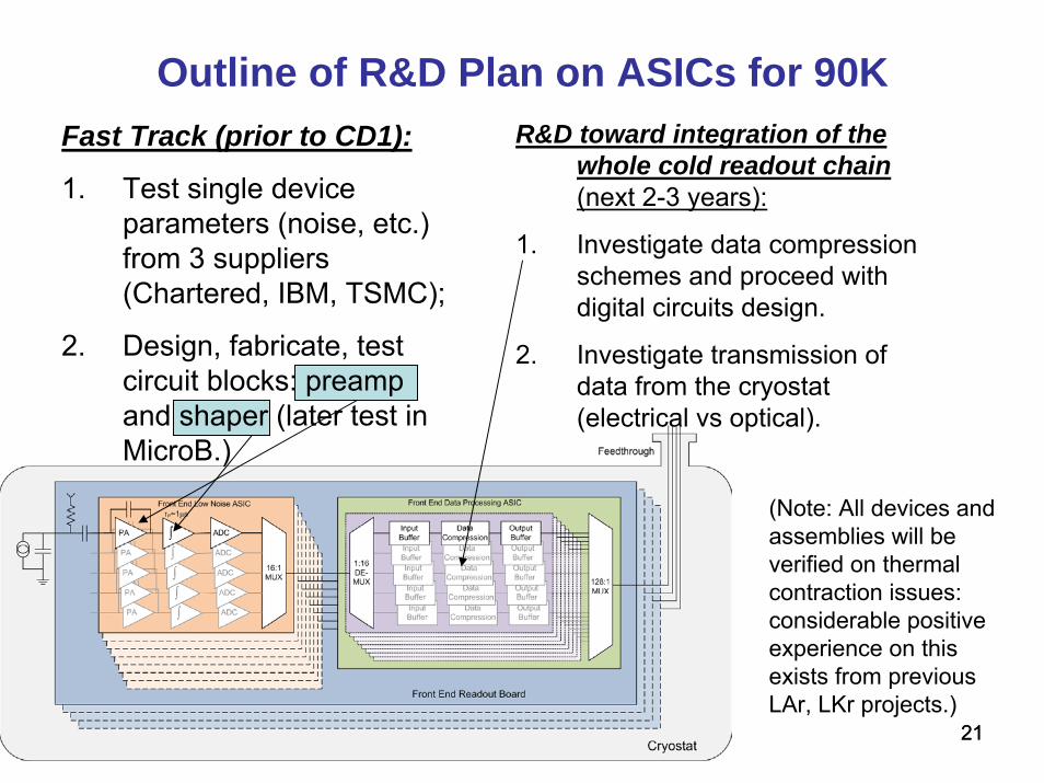
Outline of R&D Plan on ASICs for 90KFast Track (prior to CD1):
1. Test single device parameters (noise, etc.) from 3 suppliers (Chartered, IBM, TSMC);
2. Design, fabricate, test circuit blocks: preamp and shaper (later test in MicroB.)
R&D toward integration of the whole cold readout chain(next 2-3 years):
1. Investigate data compression schemes and proceed with digital circuits design.
2. Investigate transmission of data from the cryostat (electrical vs optical).
(Note: All devices and assemblies will be verified on thermal contraction issues: considerable positive experience on this exists from previous LAr, LKr projects.)