Clock Gated Single-Edge-Triggered Flip-Flop …ijeei.org/docs-609054971542a9a59a2d91.pdf · Clock...
15
International Journal on Electrical Engineering and Informatics - Volume 6, Number 3, September 2014 Clock Gated Single-Edge-Triggered Flip-Flop Design with Improved Power for Low Data Activity Applications Imran Ahmed Khan and Mirza Tariq Beg Department of Electronics and Communication, Jamia Millia Islamia, India Abstract: In this paper, the proposed flip-flop reduces power consumption by reducing the clock switching power that was wasted otherwise. Unlike many other gated flip-flops, the proposed gated flip-flop has state retention property to save power and to switch circuit between idle and active modes smoothly. The feedback path is also improved in the proposed flip-flop to decrease power dissipation. The proposed clock-gating scheme only requires 4 transistors, thus occupies the small silicon area. Further, the proposed clock gating network can be shared among a group of flip-flops to reduce the power and area overhead of the gating network. The simulation results show that for all supply voltages, the proposed flip-flop has the least power dissipation among all the designs for low switching activities. The proposed flip-flop has up to 7.82 times power improvement than the existing flip-flops. However, for 100% data activity, the proposed FF consumes up to 2.71 times power than the existing flip-flops. The proposed clock gated flip-flop structure is best suited for applications where input signal switching activity is low and speed is not a crucial factor. Keywords: Low power, CMOS digital integrated circuits, transition probability, edge triggered, storage element, VLSI 1. Introduction The rapid scaling of silicon technology has enabled designers to integrate millions and even billions of transistors into a single chip. However, while the performance increases due to scaling, the power density increases substantially every generation due to higher integration density [1]-[4]. The latest advances in mobile battery-powered devices also have set new goals in digital VLSI design. These devices require high speed and low power consumption. So, the low power design is must for the applications operated by batteries such as pocket calculators, wrist watches, mobile phones, laptops etc. It is important to prolong the battery life as much as possible [5]-[8]. All three types of power (switching power, short-circuit power and leakage power) depend upon supply voltage. The switching power of the digital chips is generally the largest portion of the power dissipation and is proportional to the square of the supply voltage. Hence, reduction of supply voltage (V DD ) is the most efficient way of reducing power consumption [9]-[11]. Unfortunately, supply voltage cannot be decreased without bound. As supply voltage is lowered, circuit delays increase leading to reduced system performance. Now power reduction is treated at all design levels of VLSI chips, from architecture through block and logic levels, down to gate-level, circuit and physical implementation [12]. To minimize the power consumption, many low-power design techniques have been introduced such as power gating [13], [14], replacing non-timing- critical cells with their high-threshold voltage counter parts [15], [16], dynamic voltage/frequency scaling [17]-[19] and clock gating [20], [21]. Among these techniques, clock gating is very important in reducing dynamic power consumption of a system on chip (SoC). Flip-flops and latches are heavily studied circuits, as they have a large impact on both cycle time and energy consumption in modern synchronous systems [22], [23]. A conventional Application Specific Integrated Circuit (ASIC) design mainly uses an edge-triggered flip-flop as a sequencing element because of the simplicity of flip-flop’s timing model. Specifically, the amount of time available to a combinational block that lies between two flip flops is fixed. This constrains timing uncertainties within each combinational block [24]. The flip flops are used extensively in all kinds of digital designs as the basic storage elements. In particular, digital designs nowadays often adopt Received: March 2 nd , 2014. Accepted: September 27 th , 2014 562
-
Upload
trinhkhanh -
Category
Documents
-
view
216 -
download
0
Transcript of Clock Gated Single-Edge-Triggered Flip-Flop …ijeei.org/docs-609054971542a9a59a2d91.pdf · Clock...

International Journal on Electrical Engineering and Informatics - Volume 6, Number 3, September 2014
Clock Gated Single-Edge-Triggered Flip-Flop Design with Improved Power for Low Data Activity Applications
Imran Ahmed Khan and Mirza Tariq Beg
Department of Electronics and Communication, Jamia Millia Islamia, India
Abstract: In this paper, the proposed flip-flop reduces power consumption by reducing the clock switching power that was wasted otherwise. Unlike many other gated flip-flops, the proposed gated flip-flop has state retention property to save power and to switch circuit between idle and active modes smoothly. The feedback path is also improved in the proposed flip-flop to decrease power dissipation. The proposed clock-gating scheme only requires 4 transistors, thus occupies the small silicon area. Further, the proposed clock gating network can be shared among a group of flip-flops to reduce the power and area overhead of the gating network. The simulation results show that for all supply voltages, the proposed flip-flop has the least power dissipation among all the designs for low switching activities. The proposed flip-flop has up to 7.82 times power improvement than the existing flip-flops. However, for 100% data activity, the proposed FF consumes up to 2.71 times power than the existing flip-flops. The proposed clock gated flip-flop structure is best suited for applications where input signal switching activity is low and speed is not a crucial factor. Keywords: Low power, CMOS digital integrated circuits, transition probability, edge triggered, storage element, VLSI
1. Introduction The rapid scaling of silicon technology has enabled designers to integrate millions and even billions of transistors into a single chip. However, while the performance increases due to scaling, the power density increases substantially every generation due to higher integration density [1]-[4]. The latest advances in mobile battery-powered devices also have set new goals in digital VLSI design. These devices require high speed and low power consumption. So, the low power design is must for the applications operated by batteries such as pocket calculators, wrist watches, mobile phones, laptops etc. It is important to prolong the battery life as much as possible [5]-[8]. All three types of power (switching power, short-circuit power and leakage power) depend upon supply voltage. The switching power of the digital chips is generally the largest portion of the power dissipation and is proportional to the square of the supply voltage. Hence, reduction of supply voltage (VDD) is the most efficient way of reducing power consumption [9]-[11]. Unfortunately, supply voltage cannot be decreased without bound. As supply voltage is lowered, circuit delays increase leading to reduced system performance. Now power reduction is treated at all design levels of VLSI chips, from architecture through block and logic levels, down to gate-level, circuit and physical implementation [12]. To minimize the power consumption, many low-power design techniques have been introduced such as power gating [13], [14], replacing non-timing-critical cells with their high-threshold voltage counter parts [15], [16], dynamic voltage/frequency scaling [17]-[19] and clock gating [20], [21]. Among these techniques, clock gating is very important in reducing dynamic power consumption of a system on chip (SoC). Flip-flops and latches are heavily studied circuits, as they have a large impact on both cycle time and energy consumption in modern synchronous systems [22], [23]. A conventional Application Specific Integrated Circuit (ASIC) design mainly uses an edge-triggered flip-flop as a sequencing element because of the simplicity of flip-flop’s timing model. Specifically, the amount of time available to a combinational block that lies between two flip flops is fixed. This constrains timing uncertainties within each combinational block [24]. The flip flops are used extensively in all kinds of digital designs as the basic storage elements. In particular, digital designs nowadays often adopt
Received: March 2nd, 2014. Accepted: September 27th, 2014
562

intensive pipelining techniques and employ many flip flops rich modules such as register file, shift register and FIFO [25], [26]. In many digital VLSI designs, the clock system that includes clock distribution network and flip-flops is one of the highest power consuming components. It accounts for 30% to 60% of the total system power, out of which 90% is consumed by the flip-flops and the last branches of the clock distribution network that are driving the flip-flops. As the power budget of today’s portable digital circuit is severely limited, it is important to reduce the power dissipation in both clock distribution networks and flip-flops [27]. This paper focuses on the minimization of power dissipation in both clock distribution network and the edge-triggered flip-flop. Clock power is a key design constraint in modern VLSI design. Despite increases in leakage power, clock power remains a significant part of the total power dissipation in modern microprocessors [28]. As timing components, flip-flops capture data with the active edge of the clock signal. Sometimes this capture is not required due to unchanged data value. Because of the constant activity of the clock signal, timing components (i.e., latches and flip-flops) are the most power-consuming components in the VLSI system [29]-[31]. Disabling the clock signal (clock gating) while the input data value matches the current state is the most obvious power reduction method. So clock-gating techniques [32] have been developed to disable unnecessary clock switching when there is no change on the input to the flip-flop. Traditionally, the system clock is connected to the clock pin on every flip-flop in the design. This results in three major components of power consumption: • Power consumed by combinatorial logic whose values are changing on each clock edge. • Power consumed by flip-flops – this has a non-zero value even if the inputs to the flip-flops are
steady and the internal state of the flip-flops is constant. • Power consumed by the clock buffer tree in the design. Clock gating has the potential of reducing both the power consumed by flip-flops and the power consumed by the clock distribution network [33]. Clock gating works by identifying groups of flip-flops sharing a common enable signal (which indicates that a new value should be clocked into the flip-flops). This enable signal is ANDed with the clock to generate the gated clock, which is fed to the clock input of all of the flip-flops that have the common enable signal. Since the data signals are provided with a temporal reference by the clock signals, the clock waveforms must be particularly clean and sharp. Gated clock contributes to clock skew and is also sensitive to glitches, which can cause design failure. So, there are several considerations in implementing clock gating. First, the enable signal should remain stable when clock is high and can only switch when clock is in low phase. Second, in order to guarantee correct functioning of the logic implementation after the gated-clock, it should be turned on in time and glitches on the gated clock should be avoided. Third, the AND gate may result in additional clock skew. For high-performance design with short-clock cycle time, the clock skew could be significant and needs to be taken into careful consideration. Clock gating network also introduces delay that affects timing performance. So, the delay in the clock gating network should be taken into careful consideration. The rest of this paper is organized as follows. Section 2 reviews previous designs of SETFFs. The proposed Clock gated SET flip-flop is discussed in section 3. Section 4 shows the simulation conditions. Section 5 shows the results and comparison. The conclusion is given in the last section. 2. Conventional Single-Edge-Triggered Flip-Flops To improve the performance of a conventional Transmission Gate Flip-Flop (TGFF shown in Figure 1) [34], [35], an inverter and transmission gate is added in [36] between the output of master latch and the output of slave latch to accomplish a push–pull effect at the slave latch. The static Push Pull Flip-Flop (PPFF) is shown in Figure 2. This increased 4 transistors. To compensate this increment of transistor count, two transmission gates are eliminated in the Push Pull Flip-Flop from the feedback paths of conventional TGFF. To save power, the number of transistors of the proposed flip-flop was reduced in [37]. The four transistors in the feedback path of conventional TGFF are replaced by single PMOS transistor. Hence, total 6 transistors are reduced in this flip-flop. This semi-static Pass Flip-Flop (Pass FF) is shown in Figure 3. To activate the feedback path of pass FF only during OFF cycle, a PMOS transistor was added in the feedback in [37]. This semi-static Pass
Imran Ahmed Khan, et al.
563

Isolation Flip-Flop (PIFF) is shown in Figure 4. As compare to Pass FF, the number of transistors of this flip-flop is increased by two but this reduces short circuit current during ON cycle. It also improves speed as compare to Pass FF. To reduce the area of the conventional TGFF, [38] removed the two feedback transmission gates of conventional TGFF. This Low-Area Flip-Flop (LAFF) is shown in Figure 5. The Area Efficient Flip-Flop (AEFF) was proposed in [39]. This semi-static flip-flop is illustrated in Figure 6. In this design the feedback circuit of the master section is removed and in slave section, feedback loop consists of a transmission gate. In Low Voltage Flip Flop (LVFF), a feedback is provided from the output node of the slave inverter to a specific internal node in the master-stage as shown in Figure 7. This flip-flop was proposed by [40]. This feedback is provided by only a single transistor. So this has lesser number of transistor as compare to other flip flops. Figure 8 shows the static C2MOS Flip-Flop [41]. This flip-flop consists of a C2MOS feedback at the outputs of the master and the slave latches. There are 20 transistors in this circuit. So C2MOSFF has largest area but this flip-flop shows the shortest delay. Area and Power Efficient Flip-Flop (APEFF), proposed by [42], is shown in Figure 9. In this flip-flop, an NMOS transistor with complemented clock signal is used to make feedback path functional only during OFF cycle of the clock. This reduces short circuit current during ON cycle. To reduce the number of transistor, only NMOS transistor is used in both master and slave latches.
Figure 1. Conventional Transmission Gate Flip-Flop (TGFF)
Figure 2. Push Pull Flip-Flop (PPFF)
Clock Gated Single-Edge-Triggered Flip-Flop Design with Improved Power
564

Figure 3. Pass Flip-Flop (Pass FF)
Figure 4. Pass Isolation Flip-Flop (PIFF)
Figure 5. Low Area Flip-Flop (LAFF)
Figure 6. Area Efficient Flip-Flop (AEFF)
Imran Ahmed Khan, et al.
565

Figure 7. Low Voltage Flip-Flop (LVFF)
Figure 8. C2MOS Flip-Flop (C2MOS FF)
Figure 9. Area and Power Efficient Flip-Flop (APEFF)
Clock Gated Single-Edge-Triggered Flip-Flop Design with Improved Power
566

Figure 10. Proposed Clock Gated SET Flip- Flop
3. Proposed Clock Gated Single-Edge-Triggered Flip-Flop Design In this paper, a new clock gated single-edge-triggered flip-flop has been developed. The clock gating technique avoids unnecessary power dissipation from clock switching. Clock gating has been shown to be an efficient technique to significantly reduce dynamic power dissipation [43]-[45]. The proposed flip-flop reduces power consumption by reducing clock switching. The feedback path is also improved in the proposed flip-flop to reduce the power consumption. The feedback loop is needed because of the drop due to the threshold of the transistors and due to the leakage in the capacitors of the transistors. Many gated flip-flops like [46] may present problem when the Control/Sleep signal is low. In these conditions the output node of the flip-flop is in a dynamic memory state and there is no possibility of any refresh operation until the sleep signals remains low. This means that sleep condition can be maintained for no more than few milliseconds. If the sleep condition is maintained for longer times:
1) The flip-flop state may not be correctly maintained during sleep 2) The transistors driven by Q output within the flip-flop and all other gates driven by the
output Q could result in a large short circuit power dissipation.
Using SETFFs with state retention property makes it possible to save power and switch circuit between idle and active modes smoothly. The proposed flip-flop has state retention property. In this structure, the circuit can be switched between idle and active modes smoothly. Most of the conventional static designs use two feedback loops one each in the master as well as the slave stage. This increases the total parasitic capacitance at the internal flip-flop nodes, leading to higher dynamic power dissipation and reduced performance. This also results in total chip area overhead due to increased transistor count [47]. In the proposed flip-flop, the feedback of master section is removed and in slave section a PMOS transistor with an inverter is used to make the flip-flop semi-static in nature. So, the feedback path is improved in the proposed flip-flop. This PMOS is grounded, so this transistor is permanently ON to reduce the switched capacitance. This further improves the power efficiency of the proposed flip-flop. In the slave latch of the proposed flip-flop, the transmission gate is used to overcome the drawbacks of the pass transistors to make the output signal clean and stable. This flip-flop is negative edge-triggered flip-flop. In Figure 10, when SLEEP input is logic LOW (SLEEPB is logic HIGH), clock is disabled and disconnected from the main circuit. When SLEEP is logic HIGH (SLEEPB is logic LOW), clock is connected to the main circuit and the circuit works in normal mode. This can be expressed mathematically by the following equations:
0, (1)
1,
Imran Ahmed Khan, et al.
567

(2)
The gated clock signal encodes whether the flip-flop retains its earlier value or takes a new input value. In the proposed FF when gated clock level is ‘HIGH’, master latch is activated and inverse of the data is stored to an intermediate node N (output of master latch). When gated clock goes to ‘LOW’ logic level, slave latch becomes functional and produces data at the output Q. Clock-gating can also help to reduce leakage power, which has an exponential dependence on the temperature [48]. Since dynamic power is reduced, the local temperature will decrease, resulting in lower leakage power. Thus leakage power is also reduced in the proposed flip-flop. The proposed clock-gating scheme only requires 4 transistors, thereby occupying less silicon area. Further, the proposed clock gating network can be shared among a group of flip-flops to reduce the power and area overhead of the gating network. If clock gating network is shared among a group of flip-flops, the result would improve drastically. Even for a single flip-flop, the proposed circuit has good improvement in power consumption for low data activity rates by reducing static and dynamic power consumption in both the clock network and the flip-flop. As stated in [49], the internal clock gating technique is appropriate for flip-flops with low switching rate in the input data. However, its advantage decreases as the switching rate increases because of the associated overhead. So, the proposed clock gated flip-flop structure is suited for applications with reduced switching activity. An example is a binary counter, in which input switching activity for each flip-flop is known beforehand. Other application includes slow-varying signals (compared with the sampling rate). This occurs, for instance, in the sampling of audio and video signals. The proposed structure can also be used in signals in which the values are most of the time close to a fixed point. This occurs, for instance, in systems that monitor physical quantities, such as temperature and pressure. 4. Simulation Conditions Simulation parameters used for comparison, are shown in Table 1. All simulations are performed on TSpice using BSIM 3v3 level 53 models in 130 nm process node. The supply voltage is varied from 1.3V to 2V. The results are carried out for the period of 16 data sequences. Under nominal condition, a 16-cycle sequence 0100000000000000 that is a low data activity is supplied at the input for average power measurements. However the dynamic power consumption is dependent on switching activities at various nodes of the circuit. It varies with different data rates and circuit topologies. Hence to obtain a fair idea of power dissipation for a circuit topology, different data patterns should be applied with different activity rates [50]. So in simulations, following four different data sequences also have been adopted to compare the power consumption of flip-flop structures discussed in this paper:
Table 1. CMOS Simulation Parameters Particulars Value Particulars Value
CMOS Technology
130 nm Nominal Supply Voltage
1.3V
Min. Gate Width 260 nm Rise Time of Clock & Data
100 ps
Max. Gate Width
1.44 µm Fall Time of Clock & Data
100 ps
MOSFET Model
BSIM 3v3 level 53
Sequence Length
16 Data Cycles
Temperature 25° C Nominal Clock Frequency
400MHz
Duty Cycle 50%
Clock Gated Single-Edge-Triggered Flip-Flop Design with Improved Power
568
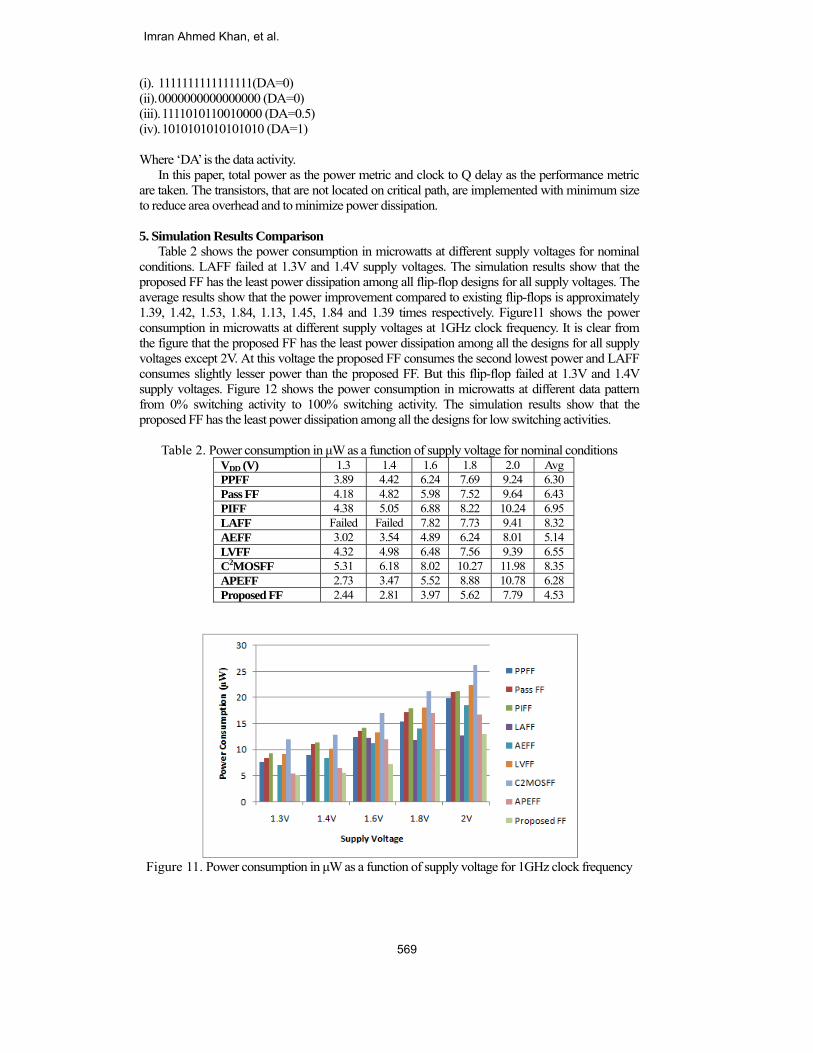
(i). 1111111111111111(DA=0) (ii). 0000000000000000 (DA=0) (iii). 1111010110010000 (DA=0.5) (iv). 1010101010101010 (DA=1) Where ‘DA’ is the data activity. In this paper, total power as the power metric and clock to Q delay as the performance metric are taken. The transistors, that are not located on critical path, are implemented with minimum size to reduce area overhead and to minimize power dissipation. 5. Simulation Results Comparison Table 2 shows the power consumption in microwatts at different supply voltages for nominal conditions. LAFF failed at 1.3V and 1.4V supply voltages. The simulation results show that the proposed FF has the least power dissipation among all flip-flop designs for all supply voltages. The average results show that the power improvement compared to existing flip-flops is approximately 1.39, 1.42, 1.53, 1.84, 1.13, 1.45, 1.84 and 1.39 times respectively. Figure11 shows the power consumption in microwatts at different supply voltages at 1GHz clock frequency. It is clear from the figure that the proposed FF has the least power dissipation among all the designs for all supply voltages except 2V. At this voltage the proposed FF consumes the second lowest power and LAFF consumes slightly lesser power than the proposed FF. But this flip-flop failed at 1.3V and 1.4V supply voltages. Figure 12 shows the power consumption in microwatts at different data pattern from 0% switching activity to 100% switching activity. The simulation results show that the proposed FF has the least power dissipation among all the designs for low switching activities.
Table 2. Power consumption in μW as a function of supply voltage for nominal conditions VDD (V) 1.3 1.4 1.6 1.8 2.0 Avg PPFF 3.89 4.42 6.24 7.69 9.24 6.30 Pass FF 4.18 4.82 5.98 7.52 9.64 6.43 PIFF 4.38 5.05 6.88 8.22 10.24 6.95 LAFF Failed Failed 7.82 7.73 9.41 8.32 AEFF 3.02 3.54 4.89 6.24 8.01 5.14 LVFF 4.32 4.98 6.48 7.56 9.39 6.55 C2MOSFF 5.31 6.18 8.02 10.27 11.98 8.35 APEFF 2.73 3.47 5.52 8.88 10.78 6.28 Proposed FF 2.44 2.81 3.97 5.62 7.79 4.53
Figure 11. Power consumption in μW as a function of supply voltage for 1GHz clock frequency
Imran Ahmed Khan, et al.
569

There is only one exception. For all ones data pattern APEFF consumes lesser power than the proposed FF. For high data activities, the proposed FF consumes the highest power. LAFF failed for theseconditions except all ones data pattern. The proposed flip-flop consumes up to 2.71 times power for higher data activities and the proposed flip-flop saves up to 6.86 times power compared to existing flip-flops for low data activities. Table 3 shows the delay in Pico second for different supply voltages at nominal conditions. Main drawback of the proposed flip-flop is the reduction of timing performances. This problem has already been reported in previous papers for gated flip-flops like in [51]. This is due to the presence of gating logic that causes a propagation delay between clock and gated clock signals. The simulation results show that the proposed FF has longer delay in most of the cases than the non-gated existing designs due to delay in clock network. For 1.3V and 1.4V supply voltages, LAFF failed. For remaining supply voltages, LAFF has longer delay than the proposed FF. For 1.6V supply voltage, the proposed FF has shorter delay as compared to PPFF, Pass FF, LAFF and AEFF. For 2V supply voltage, PPFF and LAFF have longer delay than the proposed FF. The average results show that the proposed FF has 39.92%, 53.41%, 71.32%, 25.69%, 74.46%, 91.46% and 62.06% longer delay than the flip-flops discussed in section 2 except LAFF. The proposed FF has 0.31% shorter delay than LAFF.
Figure 12. Power consumption in μW as a function of data activity
Table 3. Delay in pS as a function of supply voltage
VDD (V) 1.3 1.4 1.6 1.8 2.0 Avg PPFF 99.99 116.4 132.4 111.75 95.3 111.17 Pass FF 79.77 103.55 100.3 81.3 66.15 86.21 PIFF 63.78 43.52 9.9 78.61 69.54 53.07 LAFF Failed Failed 285.36 157.31 114.19 185.62 AEFF 293.43 193.65 98.25 58.4 43.75 137.5 LVFF 74.31 56.35 41.25 34.05 30.3 47.25 C2MOSFF 25.61 18.25 13.35 11.55 10.3 15.81 APEFF 156.93 117.39 33.15 24.63 18.92 70.20 Proposed FF 374.41 254.54 95.09 117.84 83.32 185.04
Table 4 shows the power consumption in microwatts at different supply voltages for 0% data activity and 1GHz clock frequency. The simulation results show that the proposed FF has the least power dissipation among all the designs for all supply voltages. The average results show that the power improvement compared to existing flip-flops is approximately 4.80, 5.53, 5.90, 5.26, 4.44, 5.84, 7.10 and 3.40 times respectively. The proposed flip-flop has up to 7.82 times power
Clock Gated Single-Edge-Triggered Flip-Flop Design with Improved Power
570

improvement compared to existing flip-flops.
Table 4. Power consumption in µW as a function of supply Voltage for 0% data activity and 1GHz clock frequency
VDD (V) 1.3 1.4 1.6 1.8 2.0 PPFF 6.79 7.89 11.09 13.73 17.90 Pass FF 7.87 10.46 12.56 15.9 19.33 PIFF 8.68 11.07 13.25 16.86 20.63 LAFF Failed 8.02 11.08 13.98 17.14 AEFF 6.66 7.89 10.33 12.38 15.86 LVFF 8.68 9.71 12.56 17.36 21.51 C2MOSFF 11.1 12.35 16.21 20.19 24.95 APEFF 4.27 4.99 9.57 12.19 9.65 Proposed FF 1.42 1.8 2.32 2.8 3.62
Figure 13. Power consumption in µW as a function of supply Voltage for 0% data activity and
400MHz clock frequency
Figure 13 shows the power consumption in microwatts at different supply voltages for 0% data activity and 400MHz clock frequency. The simulation results show that the proposed FF has the least power dissipation and C2MOSFF has the highest power dissipation among all the designs for all supply voltages. Figure 14 shows the power consumption in microwatts at different clock frequencies for nominal conditions. It is clear from the figure that the proposed FF has the least power dissipation among all the designs for all clock frequencies except 100MHz. At this clock frequency the proposed FF consumes the second lowest power and AEFF consumes slightly lesser power than the proposed FF. For these conditions LAFF completely failed. C2MOSFF consumes the highest power at all clock frequencies.
Imran Ahmed Khan, et al.
571

Figure 14. Power consumption in μW as a function of clock frequency
6. Conclusion Synchronous systems require the clock that dictates the temporal behavior of the system. A significant amount of energy is wasted for proper synchronization among different components. The clock gating technique avoids unnecessary power dissipation from clock switching. In this paper, a new clock gated single-edge-triggered flip-flop has been developed to reduce the waste of energy in flip-flops with low data activity. The proposed flip-flop reduces power consumption by reducing the clock switching. Unlike many other gated flip-flops, the proposed flip-flop has state retention property to save power and to switch circuit between idle and active modes smoothly. The feedback path is also improved in the proposed flip-flop to decrease the total parasitic capacitance at the internal flip-flop nodes and to reduce dynamic power dissipation. In the slave latch of the proposed flip-flop, the transmission gate is used to overcome the drawbacks of the pass transistors to make the output signal clean and stable. The proposed clock-gating scheme only requires 4 transistors, thereby occupying less silicon area. Further, the proposed clock gating network can be shared among a group of flip-flops to reduce the power and area overhead of the gating network. If clock gating network is shared among a group of flip-flops, the result would be more interesting. Even for a single flip-flop, the proposed circuit has good improvement in power consumption for low data activity rates by reducing static and dynamic power consumption in both the clock network and the flip-flop. The simulation results show that for all supply voltages, the proposed FF has the least power dissipation among all the designs for low switching activities. The proposed flip-flop has up to 7.82 times power improvement than the existing flip-flops for low data activity applications. However the proposed FF is not suited for higher data activity applications. The proposed FF consumes higher power for 50% and 100% data activities as compared to existing flip-flops. For these two higher data activities, the proposed FF consumes 2.42 and 2.71, times power than the existing flip-flops respectively. Gated flip-flops present a significant increase of timing parameters. This is due to the presence of gating logic that causes a propagation delay between clock and gated clock signals. The simulation results show that the proposed FF has longer delay in most of the cases than the existing non-gated designs due to delay in clock network. The proposed flip-flop has up to 14.62 times longer delay. However in many cases the proposed flip-flop has shorter delay than the existing flip-flops and the proposed flip-flop has up to 3.0 time shorter delay. By clock gating technique a significant power dissipation reduction is obtained if input signal switching activity is low. However, its advantage decreases as the switching rate increases because of the associated overhead. So, the proposed clock gated flip-flop structure is best suited for applications where input signal switching activity is low. An example is a binary counter, in which input switching activity for each flip-flop is known beforehand. Other application includes slow-varying signals (for instance, in the sampling of audio and video signals). This flip-flop can also be
Clock Gated Single-Edge-Triggered Flip-Flop Design with Improved Power
572

used in signals where the values are most of the time close to a fixed point (for instance in systems that monitor physical quantities, such as temperature and pressure). As a conclusion proposed flip-flop is best suited for applications in which input activity is kept low and speed is not a crucial factor. 7. References [1] B. C. Paul, A. Agarwal and K. Roy, “Low-power design techniques for scaled technologies,”
Integration, the VLSI journal, Elsevier, Vol. 39, issue 2, March, 2006, pp. 64–89. [2] M. Lanuzza R.D. Rose, F. Frustaci, S. Perri and P. Corsonello, “Comparative analysis of yield
optimized pulsed flip-flops,” Microelectronics Reliability, Elsevier, Volume 52, Issue 8, August 2012, pp. 1679–1689.
[3] B. Brindha V. S .K. Bhaaskaran, C. Vinoth, V. Kavinilavu, S. Sakthikumaran, “Optimization of Sense Amplifier Energy Recovery Flip-Flop,” 3rd International Conference on Electronics Computer Technology (ICECT), IEEE Conference, April 2011, pp. 317-319.
[4] P. Zhao, J. B. McNeely, P. K. Golconda, S. Venigalla, N. Wang, M.A. Bayoumi,W. Kuang and L. Downey, “Low Power clocked Pseudo NMOS flip flop for level conversion in dual supply systems,” IEEE Transaction on Very Large Scale Integration(VLSI) systems, Vol. 17, No.9, September 2009, PP 1196-1202.
[5] A. M. Khedr and W. Osamy, “Tracking Mobile Targets Using Sensor Networks” The Arabian Journal for Science and Engineering, Vol. 32, No. 2B, pp. 301-305, 2007.
[6] L. T. Wang, Y. W. Chang and K. T. Cheng, Eds., “Electronic Design Automation: Synthesis, Verification, and Test” Burlington, MA: Elsevier/Morgan Kaufmann, 2009.
[7] I. H. R. Jiang, C. L. Chang and Y. M. Yang, “Integra: Fast Multibit Flip-Flop Clustering for Clock Power Saving” IEEE Transactions on Computer-Aided Design of Integrated Circuits and Systems, Vol. 31, No. 2, pp. 192-204, Feb. 2012.
[8] Abhilasha, K. G. Sharma, T. Sharma and B.P. Singh, “Low Power 6-Transistor Latch Design for Portable Devices” Innovative Systems Design and Engineering (ISDE), Vol. 3, No 5, pp 68-83, 2012.
[9] T. Y. Kuo and J. S. Wang, “A Low-Voltage Latch-Adder Based Tree Multiplier” IEEE International Symposium on Circuits and Systems (ISCAS), pp. 804-807, 2008.
[10] T. V. Cao, D. T. Wisland, F. Moradi and T. S. Lande, “Novel Low Voltage Current-Mirror Sense Amplifier based Flip-Flop with Reduced Delay Time” IEEE International Symposium on Circuits and Systems (ISCAS), pp. 3166-3169, 2009.
[11] A. Chandrakasan, W. Bowhill, F. Fox, “Design of High-Performance Microprocessor Circuits” 1st ed. Piscataway, NJ: IEEE, 2001.
[12] S. Wimer and I. Koren, “The Optimal Fan-Out of Clock Network for Power Minimization by Adaptive Gating” IEEE Transaction on Very Large Scale Integration (VLSI) Systems, Vol. 20, No. 10, pp. 1772-1780, 2012.
[13] D. S. Chiou, S. H. Chen, S. C. Chang and C. Yeh, “Timing driven power gating,” in Proc. ACM/IEEE Design Automation Conference, Sep. 2006, pp. 121–124.
[14] H. Xu, R. Vemuri and W. Jone, “Dynamic characteristics of power gating during mode transition,” IEEE Transaction on Very Large Scale Integration (VLSI) Systems, Vol. 19, No. 2, Feb. 2011, pp. 237–249.
[15] A. Khan et al., “A 90 nm power optimization methodology with application to the ARM 1136JF-S microprocessor,” IEEE J. Solid-State Circuits, Vol. 41, No. 8, Aug. 2006, pp. 1707–1717.
[16] T. Luo, D. Newmark and D. Z. Pan, “Total power optimization combining placement, sizing and multi-Vt through slack distribution management,” in Proc. IEEE/ACM Asia South Pacific Design Automation Conference, Mar. 2008, pp. 352–357.
[17] G. Magklis, G. Semeraro, D. H. Albonesi, S. G. Dropsho, S. Dwarkadas and M. L. Scott “Dynamic Frequency and Voltage Scaling for a Multiple-Clock-Domain Microprocessor” IEEE Micro Vol. 23 , No. 6, November–December 2003, pp. 62-68.
[18] G. Magklis, M. L. Scott, G. Semeraro, D. H. Albonesi and S. Dropsho, “Profile-based dynamic voltage and frequency scaling for a multiple clock domain microprocessor,”
Imran Ahmed Khan, et al.
573

Proceeding of the 30th Annual Inernational Symposium on Computer Architecture, New York, USA, May, 2003, pp. 14–27.
[19] L. Yan, J. Luo and N. Jha, “Combined dynamic voltage scaling and adaptive body biasing for heterogeneous distributed real-time embedded systems,” IEEE/ACM International Conference on Computer-Aided Design, Nov. 2003, pp. 30–37.
[20] Q. Wu, M. Pedram and X. Wu, “Clock-gating and its application to low power design of sequential circuits,” IEEE Transaction on Circuits and System I, Vol. 47, No. 103, Mar. 2000, pp. 415–420.
[21] H. Mahmoodi, V. Tirumalashetty, M. Cooke and K. Roy, “Ultralowpower clocking scheme using energy recovery and clock gating,” IEEE Transaction on Very Large Scale Integration (VLSI) Systems, Vol. 17, No. 1, Jan.2009, pp. 33–44.
[22] H. Kawaguchi and T. Sakurai, “A reduced clock-swing flip-flop (RCSFF) for 63% power reduction,” IEEE Journal of Solid-State Circuits, Vol. 33, No. 5, May 1998, pp. 807–811.
[23] T. Lang, E. Musoli, and J. Cortadella, “Individual flip-flops with gated clocks for low power datapaths,” IEEE Transaction on Circuits and Systems II, Analog and Digital Signal Processing, Vol. 44, No. 6, Jun. 1997, pp. 507–516.
[24] Y. Shin and S. Paik, “Pulsed-Latch Circuits: A New Dimension in ASIC Design” IEEE Design and Test of Computers, Vol. 28, No. 6, pp 50-57, 2011.
[25] J. F. Lin, “Low-Power Pulse-Triggered Flip-Flop Design Based on a Signal Feed-Through Scheme” IEEE Transaction on Very Large Scale Integration (VLSI) Systems, Vol. 22, No. 1, pp. 181 – 185, 2014.
[26] Y. T. Hwang, J. F. Lin and M. H. Sheu, “Low-Power Pulse-Triggered Flip-Flop Design With Conditional Pulse-Enhancement Scheme” IEEE Transaction on Very Large Scale Integration (VLSI) Systems, Vol. 20, No. 2, pp. 361-366, Feb. 2012.
[27] M. W. Phyu, K. Fu, W. L. Goh and K. S. Yeo, “Power-Efficient Explicit-Pulsed Dual-Edge Triggered Sense-Amplifier Flip-Flops”, IEEE Transaction on Very Large Scale Integration (VLSI) Systems, Vol. 19, No. 1, 2011, pp. 1-9.
[28] D. Brooks et al., “Power-Aware Microarchitecture: Design and Modeling Challenges for Next Generation Microprocessors,” IEEE Micro, Vol. 20, No. 6, November-December 2000, pp. 26-44.
[29] V. Zyuban et al., “Integrated analysis of power and performance for pipelined microprocessors,” IEEE Transactions on Computers, Vol. 53, August 2004, pp. 1004-1016.
[30] V. Tiwari, D. Singh, S. Rajgopal, G. Mehta, R. Patel and F. Baez, “Reducing power in high-performance microprocessors,” 35th Annual Design Automation Conference, San Francisco, CA, June 1998, pp. 732-737.
[31] X. Wang and W.H. Robinson, “A Low-Power Double Edge-Triggered Flip-Flop with Transmission Gates and Clock Gating” 53rd IEEE International Midwest Symposium on Circuits and Systems (MWSCAS), pp 205-208, 2010.
[32] A. S. Seyedi, S. H. Rasouli, A. Amriabadi and A. Afzali-Kusha, “Clock Gated Static Pulsed Flip-Flop (CGSPFF) in Sub 100 nm Technology,” in the Proceedings of IEEE Computer Society Annual Symposium on Emerging VLSI Technologies and Architectures, Germany, March 2006, pp. 373 – 377.
[33] P. R. Panda, B. V. N. Silpa, A. Shrivastava, K. Gummidipudi, Power-efficient System Design, New York, Springer, 2010.
[34] D. S. Valibabal, S. Sivanantham, P. S. Mallick and J. R. P. Perinbam, “Reduction of Testing Power with Pulsed Scan Flip-flop for Scan Based Testing,” IEEE International Conference on Signal Processing, Communication, Computing and Networking Technologies (ICSCCN),Thuckafay, July 2011, pp. 526-531.
[35] S. Hsu and S. L. Lu, “A Novel High-Performance Low-Power CMOS Master-Slave Flip-Flop,” Twelfth Annual IEEE International ASIC/SOC Conference, Washington, DC, September 1999, pp. 340-343.
[36] U. Ko and P. T. Balsara, “High-Performance Energy- Efficient D-Flip-Flop Circuits,” IEEE Transaction on Very Large Scale Integration (VLSI) Systems, Vol. 8, No. 1, Feb. 2000, pp. 94-
Clock Gated Single-Edge-Triggered Flip-Flop Design with Improved Power
574

h
98. [37] S. Agarw
PerformanAdvanced
[38] G. GerosaCircuits, V
[39] M. SharmSingle EdTechnolog
[40] K. Singh,with ImpIssue on R
[41] R. RamanSoft Error(SOC) Co
[42] I. A. KhanStructure Design an
[43] A. Chand1998.
[44] A. CorreaPowerPCElectronic
[45] M. GowaMicropro726–731.
[46] M. Hansson-Chip C
[47] K. Singh,Voltage SIEEE conf
[48] S. Heo, KProceedinAug 2003
[49] D. MarkoThesis, U
[50] V. StojanoFlops for Vol. 34, N
[51] M. NogawReductionMay, 199
has authored m
wal, P. Ramanathnce Flip–Flopsd Computing ana et al., “2.2 W,Vol. 29, No. 12, ma, A. Noor, S.dge Triggered Dgies in Commun, S. C. Tiwari a
proved Power-DRecent Trends innarayanan, V. Dr Rate in Flip-Fonference, Sep. n and M. T. Begfor Low Data
nd Engineering,drakasan and R
ale Jr., “OvervC 4xx embeddecs and Design (Ian, L. Biro and Dcessor,” Procee
son and A. AhaConference, San, S. C. Tiwari aystems,” World
nference, MumbK. Barr and K. ng of the Interna3, pp. 217-222. ovic, Analysis
University of Calovic and V.G. OHigh-Performa
No. 4, April, 199awa and Y. Ohn in Power Con8, pp. 702-706.
Imran AElectronicand M.TeNew Delhalso workCommunidegree in research in
many papers in in
than and P. T. Vs in the 0.13µmnd Communicat
W, 80 MHz superDec. 1994, pp.
. C. Tiwari andD-Flip-flop,” IEnication and Coand M. Gupta, “Delay Product,”n VLSI Design)
Degalahal, N. VFlops and Scan2003, pp. 231-2g, “A New Areaa Activity and , Vol. 4, No. 1, J
R. Brodersen, L
view of the powed controllers,” (ISLPED), DanaD. Jackson, “Poeding of 35th De
andpour, “A Lonta Clara, CA, Uand M. Gupta, “d Congress on Inbai, India, Decem
Asanovic, “Reational Symposi and Design of
lifornia at BerkeOklobdzija, “Comance and Low-P99, pp. 536-548.htomo, “A Datansumption,” IE
Ahmed Khancs & Communicech degree fromhi, India in 2009ked as assistanication at U.P. Tthe field of lownterests includenternational Jou
Vanathi, “Compm Technology”tions, Guwahatirscalar RISC pr1440–1454.
d K. Singh, “AnEEE Internationomputing, Kotta“A Master-Slav” World Applie), 2012, pp: 45-
Vijaykrishnan, Mnnable Latches,”234.4 a and Power EffHigh Frequen
Jan. 2013, PP. 1Low Power CM
wer minimizatiIn Proc. Inter
a pt., CA, USA, ower Consideratesign Automatio
ow Clock Load USA, Septembe“A High Perfornformation andmber 2011, pp. educing Power ium on Low Po
f Low-Energy eley, 2001 mparative Anal
Power Systems,. a-Transition Lo
EEE Journal of
received his Bcation, Jamia Mm VLSI departm9. In 2009 he jont Professor inTechnical Univ
w power designe low power digurnals and proce
parative Analys”, IEEE Intern, Assam, Dec. 2rocessor,” IEEE
n Area and Ponal Conference ayam, Kerala, Ove Flip Flop fored Sciences Jou52.
M. J. Irwin and D” IEEE Interna
fficient Single Edncy Application-12.
MOS Design, N
ion techniques rnational SympApril 1995, pp.
ations in the Deson Conference (D
Conditional Flier 12-15, 2004.rmance Flip Flod Communicatio257-262. Density throug
ower Electronics
Clocked Stora
lysis of Master-” IEEE Journa
ook-Ahead DFFf Solid-State Cir
B.Tech degreeMillia Islamia, N
ment, G.G.S. Ioined Cadence n the departm
versity. He is cun from Jamia Mgital and mixed
eedings of intern
sis of Low Pownational Confer2007, pp. 209-2E Journal of So
ower Efficient don Advances in
Oct. 2009, 478-4r Low Voltage urnal, Vol. 16
D. Duarte, “Anational Systems-
dge Triggered Fns,” Innovative
New York, IEEE
employed in tposium on Low. 75–80. sign of the Alph(DAC), June 199
ip-Flop,” IEEE
op for Low Powon Technologies
gh Activity Migs and Design (I
age Elements, M
-Slave Latches al of Solid-State
F Circuit for Srcuits, Vol. 33,
e from DepartmNew Delhi, IndiaIndraprastha UnDesign System
ment of Electrourrently pursuin
Millia Islamia, Ind signal IC desnational confere
wer High rence on 13.
olid-State
design of n Recent 481. Systems (Special
nalysis of -on-Chip
Flip-Flop Systems
E Press.,
the IBM w Power
ha 21264 98, pp.
E System-
wer Low s (WICT),
gration”, SLPED),
Master’s
and Flip-Circuits,
Statistical Issue 5,
ment of a in 2006 niversity,
m. He has onics & ng Ph.D. ndia. His igns. He
ences.
Imran Ahmed Khan, et al.
575

Journals a
MirzDelhand BcareeIslamthe sComHe h
and proceedings
za Tariq Beg rhi in the year 20B.Tech from Aer as an Assistanmia, New Delhi same organizat
mmunication andhas authored as of conferences
received his Ph.003, M.Tech fro
Aligarh Muslim nt Professor in tin 1987. Curren
tion. He is wod Computer Neand co-authores.
.D. degree fromom Delhi UniveUniversity, Ali
the Departmentntly he is workinorking in area etworks as well ed many pape
m Jamia Millia ersity, Delhi in tigarh in 1985. Ht of E & C fromng as Professor of Microwave as low power d
ers in Internati
Islamia, New the year 1987 He started his
m Jamia Millia r since 2003 in
Engg., Data digital design. ional/National
Clock Gated Single-Edge-Triggered Flip-Flop Design with Improved Power
576