Lecture 10: Sequential Elements (Latches and Flip...
52
VLSI-1 Class Notes Lecture 10: Sequential Elements (Latches and Flip Flops) Mark McDermott Electrical and Computer Engineering The University of Texas at Austin 10/2/18
Transcript of Lecture 10: Sequential Elements (Latches and Flip...
VLSI-1 Class Notes
Lecture 10:Sequential Elements (Latches and Flip Flops)
Mark McDermottElectrical and Computer Engineering
The University of Texas at Austin
10/2/18
VLSI-1 Class Notes
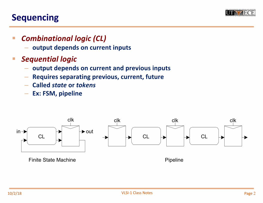
Sequencing
§ Combinational logic (CL)– output depends on current inputs
§ Sequential logic– output depends on current and previous inputs– Requires separating previous, current, future– Called state or tokens– Ex: FSM, pipeline
CL
clk
in out
clk clk clk
CL CL
PipelineFinite State Machine
10/2/18 Page 2
VLSI-1 Class Notes
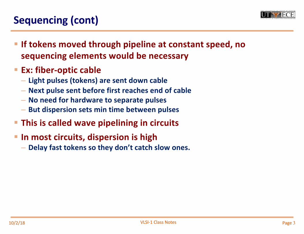
Sequencing (cont)
§ If tokens moved through pipeline at constant speed, no
sequencing elements would be necessary
§ Ex: fiber-optic cable
– Light pulses (tokens) are sent down cable
– Next pulse sent before first reaches end of cable
– No need for hardware to separate pulses
– But dispersion sets min time between pulses
§ This is called wave pipelining in circuits
§ In most circuits, dispersion is high
– Delay fast tokens so they don’t catch slow ones.
10/2/18 Page 3
VLSI-1 Class Notes
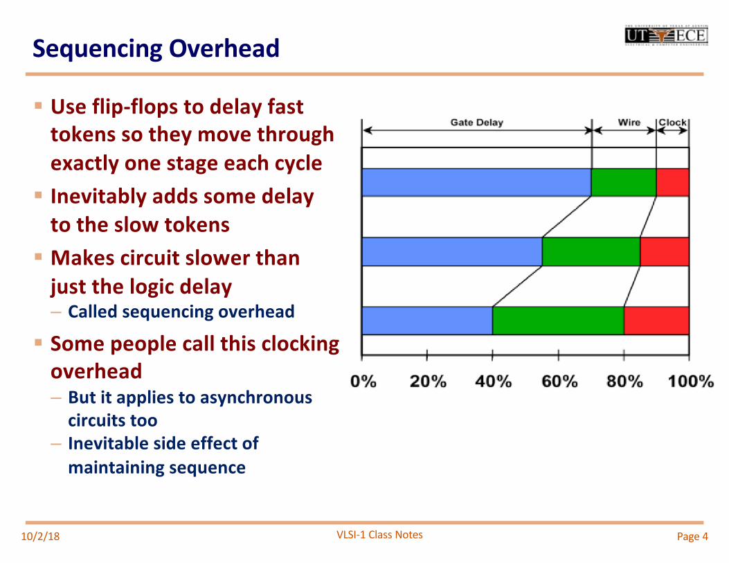
Sequencing Overhead
§ Use flip-flops to delay fast tokens so they move through exactly one stage each cycle
§ Inevitably adds some delay to the slow tokens
§ Makes circuit slower than just the logic delay– Called sequencing overhead
§ Some people call this clocking overhead– But it applies to asynchronous
circuits too– Inevitable side effect of
maintaining sequence
Page 410/2/18
VLSI-1 Class Notes
clock
Dout
Din
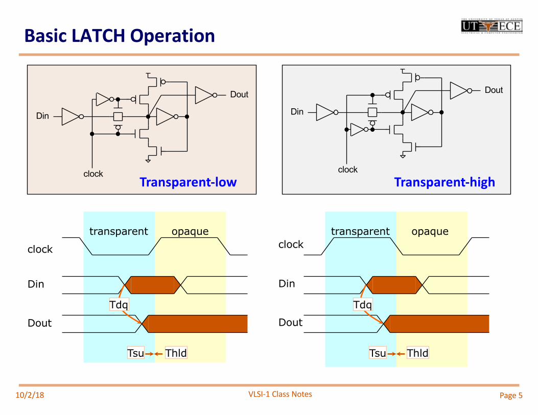
Transparent-low
clock
transparent opaque
Din
Dout
Tsu Thld
Tdq
clock
Dout
Din
Transparent-high
transparent opaqueclock
Din
Dout
Tsu Thld
Tdq
Basic LATCH Operation
10/2/18 Page 5
VLSI-1 Class Notes
Din
Dout
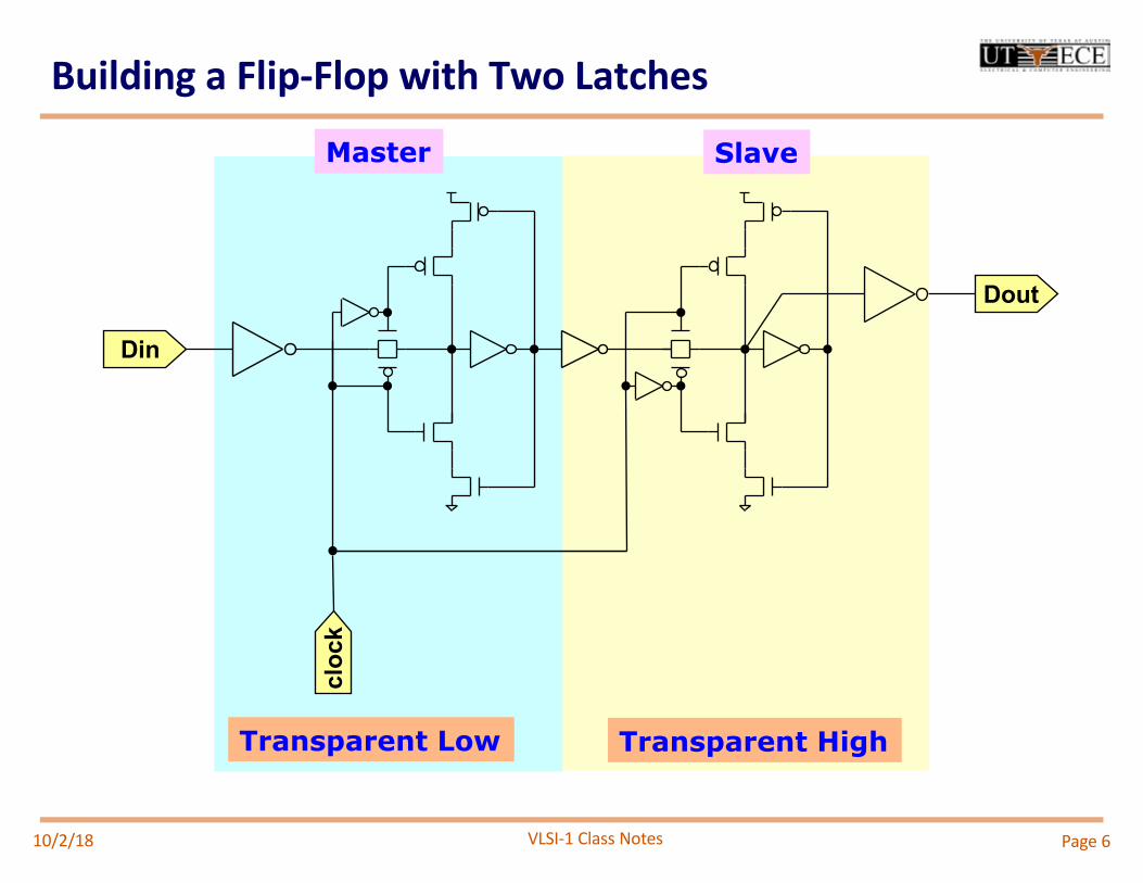
Building a Flip-Flop with Two Latches
clock
Transparent HighTransparent Low
10/2/18 Page 6
SlaveMaster
VLSI-1 Class Notes Page 7
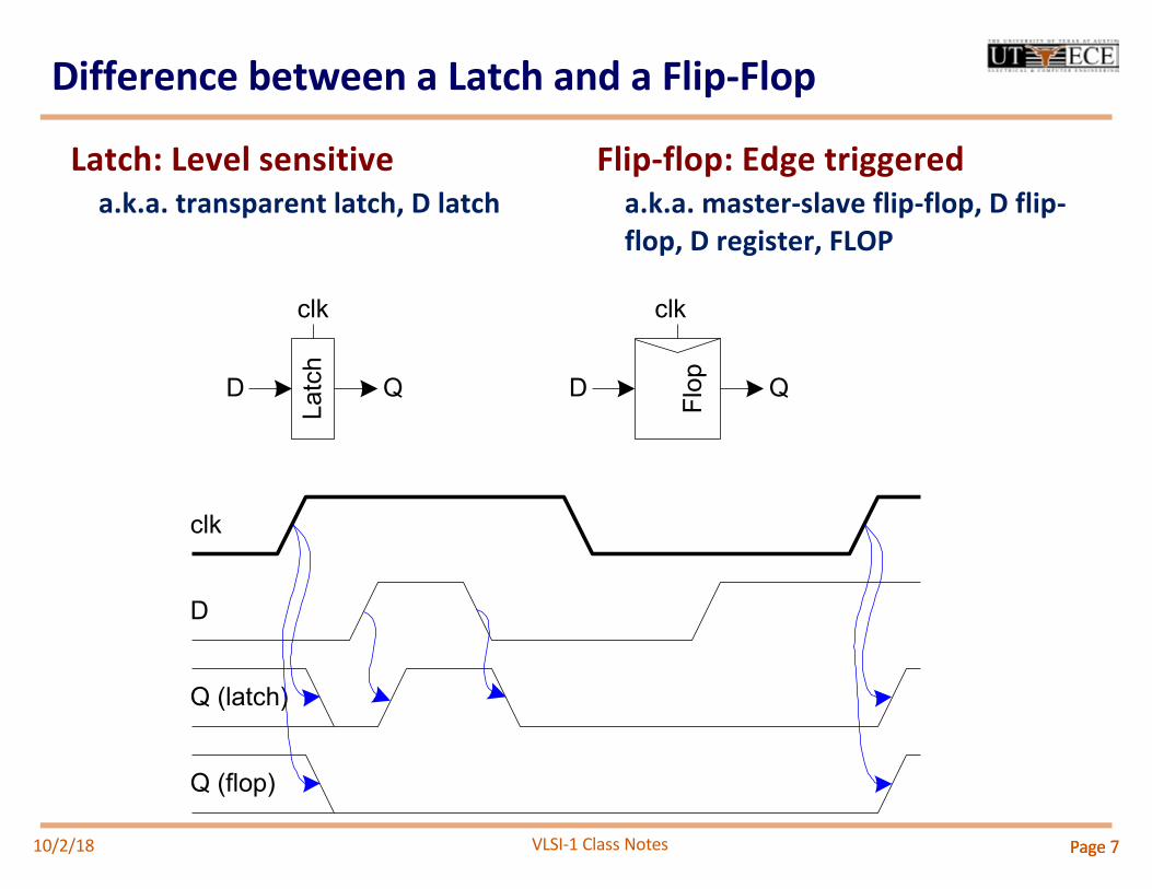
Difference between a Latch and a Flip-Flop
Latch: Level sensitivea.k.a. transparent latch, D latch
Flip-flop: Edge triggereda.k.a. master-slave flip-flop, D flip-flop, D register, FLOP
10/2/18 Page 7
D Flop
Latc
h
Q
clk clk
D Q
clk
D
Q (latch)
Q (flop)
VLSI-1 Class Notes
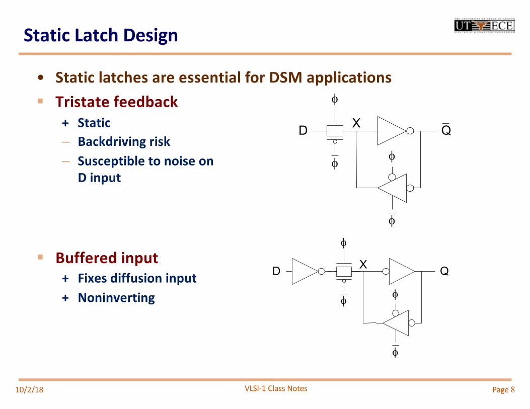
Static Latch Design
f
f
QD X
f
f
§ Tristate feedback+ Static– Backdriving risk– Susceptible to noise on
D input
§ Buffered input+ Fixes diffusion input+ Noninverting
f
f f
f
QD X
• Static latches are essential for DSM applications
10/2/18 Page 8
VLSI-1 Class Notes
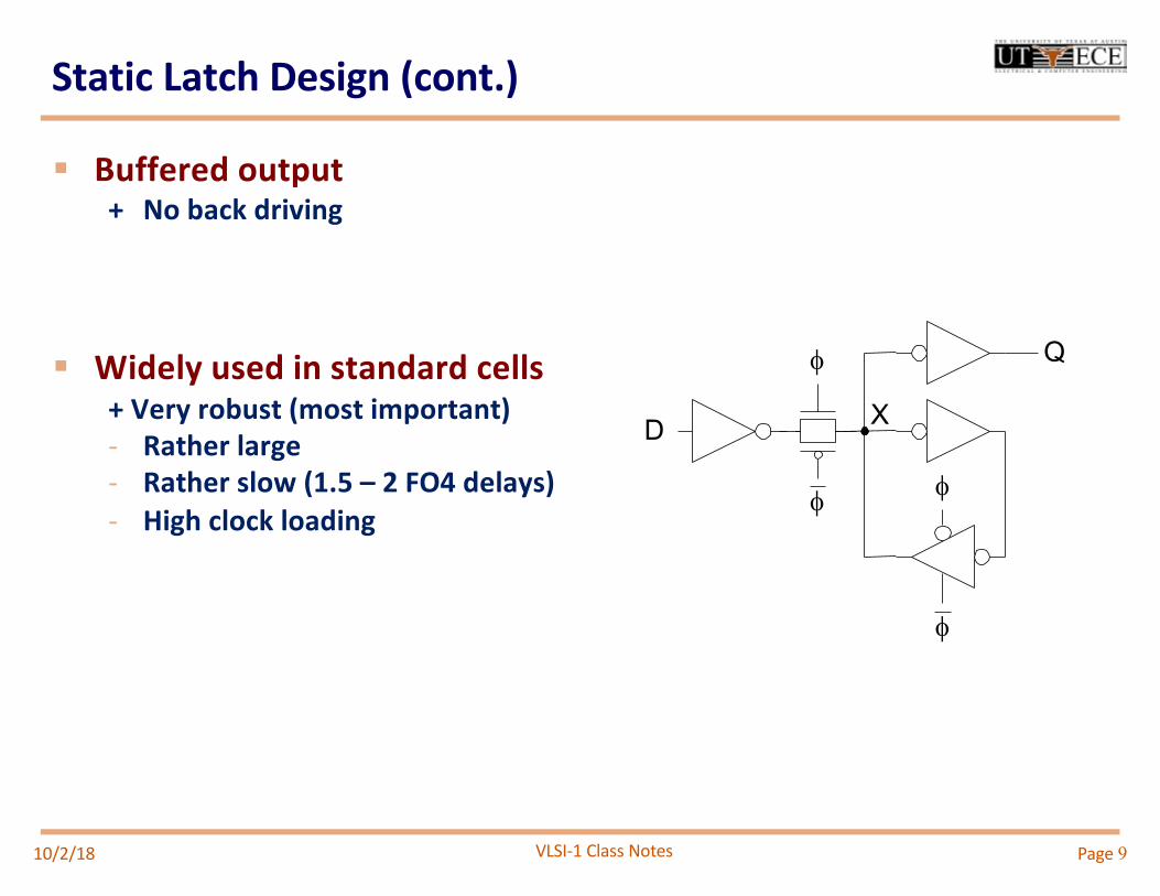
Static Latch Design (cont.)
§ Buffered output+ No back driving
§ Widely used in standard cells+ Very robust (most important)- Rather large- Rather slow (1.5 – 2 FO4 delays)- High clock loading
f
f
Q
D X
f
f
10/2/18 Page 9
VLSI-1 Class Notes
Static Latch Design (cont.)
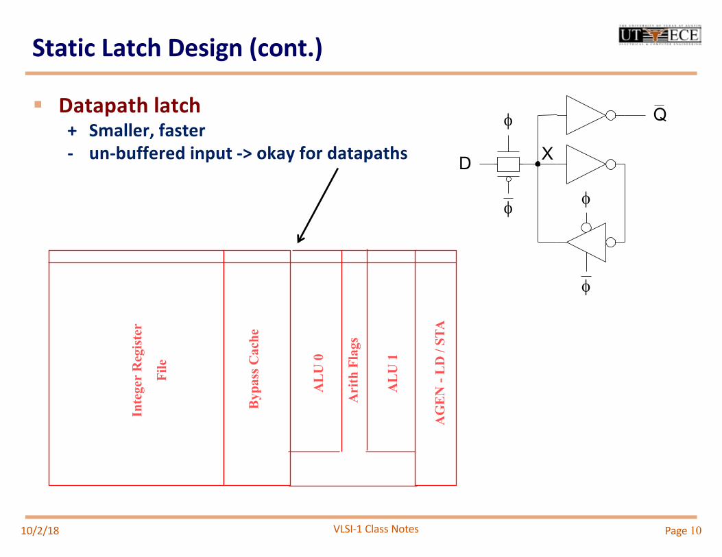
§ Datapath latch+ Smaller, faster- un-buffered input -> okay for datapaths
f
f f
f
Q
D X
10/2/18 Page 10
Bypa
ss C
ache
Inte
ger R
egist
er
File
ALU
0
ALU
1
Ari
th F
lags
AG
EN -
LD /
STA
VLSI-1 Class Notes
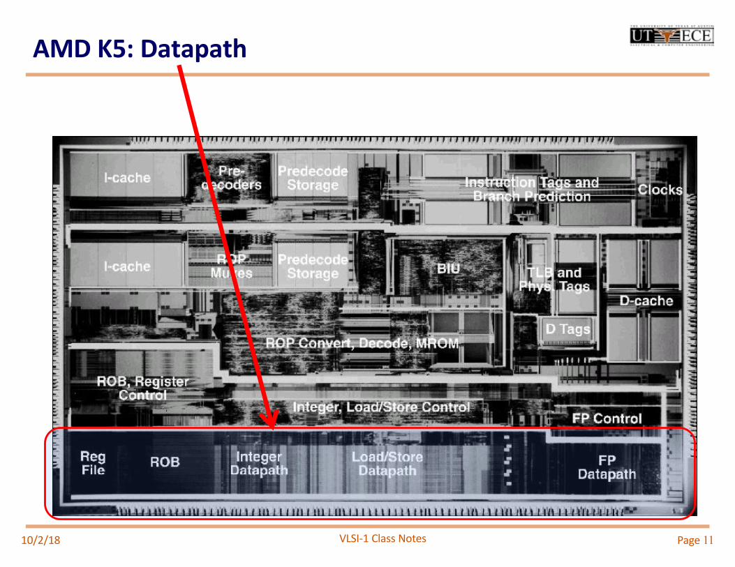
AMD K5: Datapath
Page 1110/2/18
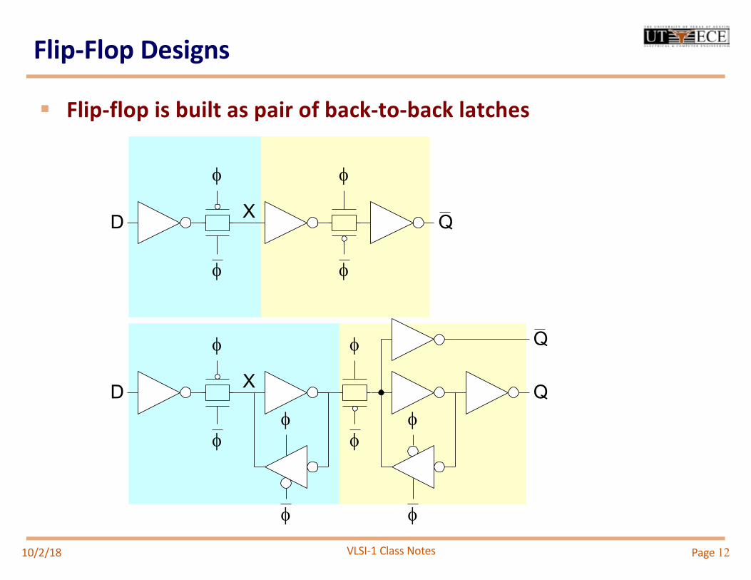
VLSI-1 Class Notes
§ Flip-flop is built as pair of back-to-back latches
Flip-Flop Designs
10/2/18 Page 12
D Q
f
f
f
f
X
D
f
f
f
f
X
Q
Qf
f
f
f
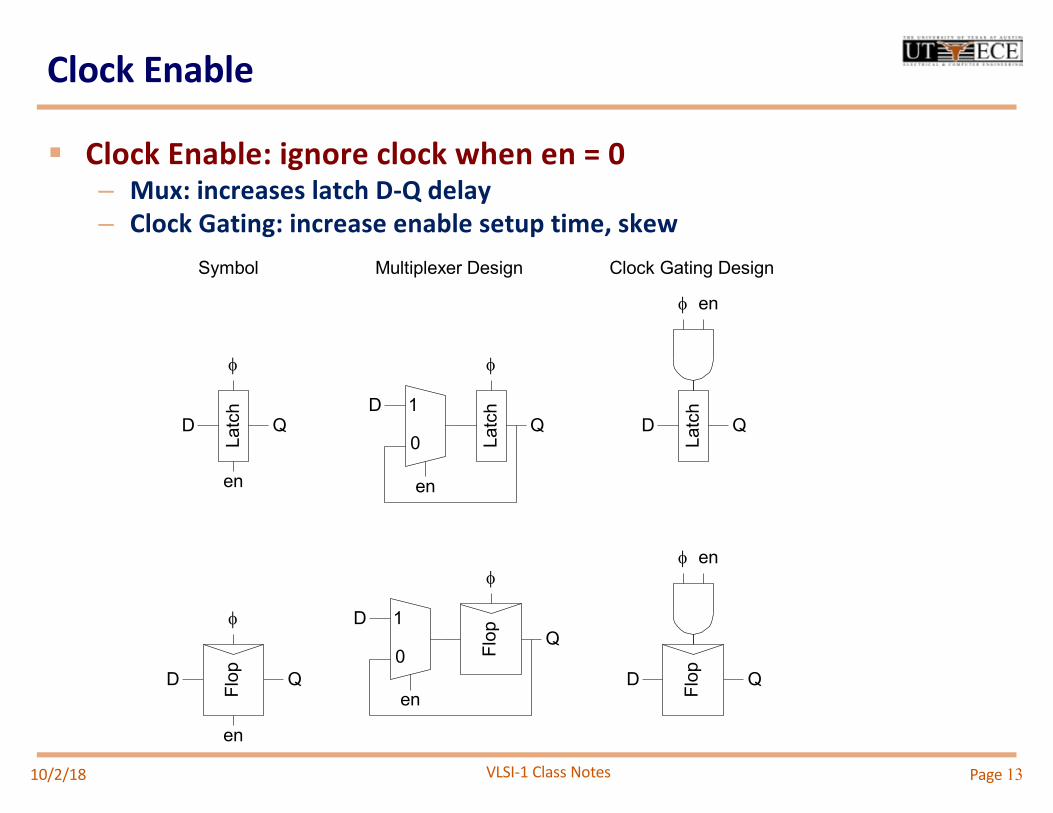
VLSI-1 Class Notes
Clock Enable
§ Clock Enable: ignore clock when en = 0– Mux: increases latch D-Q delay– Clock Gating: increase enable setup time, skew
D Q
Latc
h
D Q
en
en
f
f
Latc
hDQ
f
0
1
en
Latc
h
D Q
f en
DQ
f
0
1
enD Q
f en
Flop
Flop
Flop
Symbol Multiplexer Design Clock Gating Design
10/2/18 Page 13
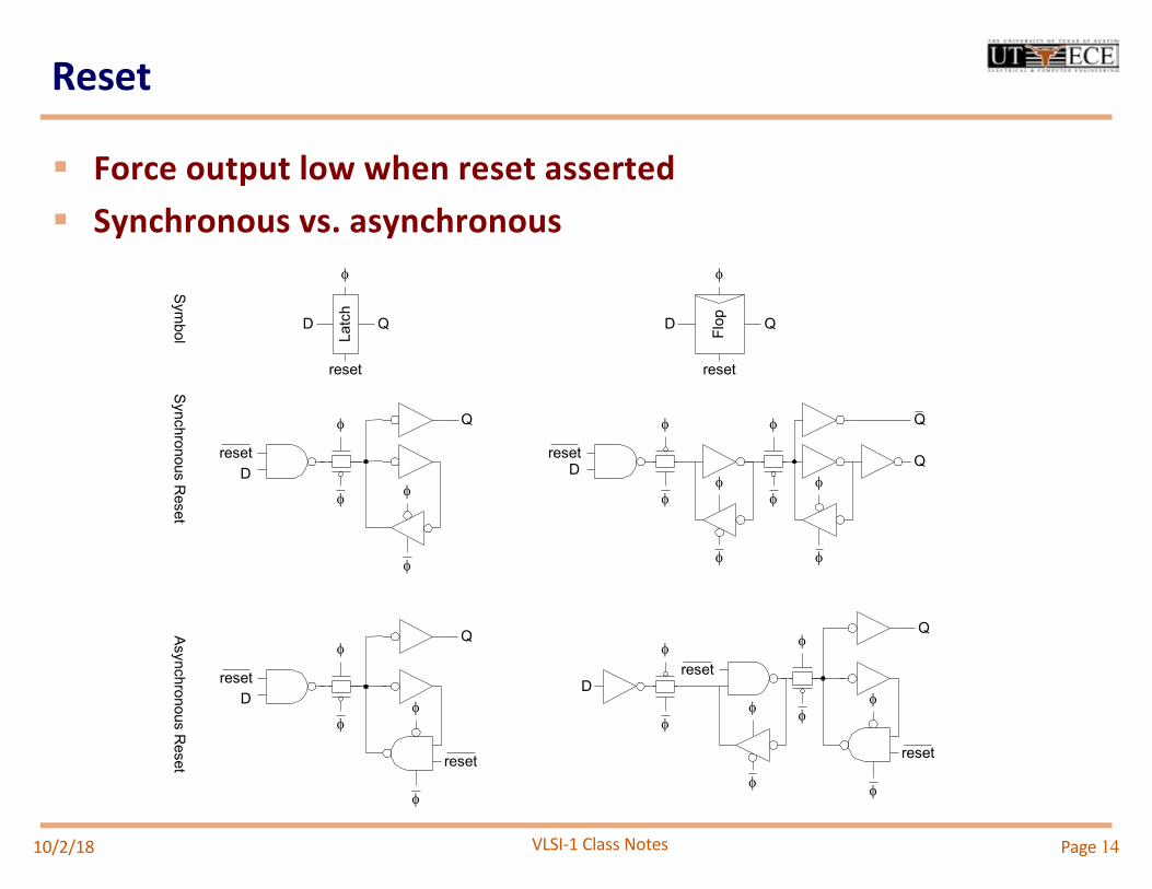
VLSI-1 Class Notes
Reset
§ Force output low when reset asserted§ Synchronous vs. asynchronous
D
f
f
f
f
Q
Qf
f
f
f
reset
D
f
ff
f
f
f
Qf
f
Dreset
f
f
Qf
f
Dreset
reset
f
f
reset
Synchronous Reset
Asynchronous Reset
Symbol Fl
opD QLa
tch
D Q
reset reset
f f
f
f
Q
reset
10/2/18 Page 14
VLSI-1 Class Notes
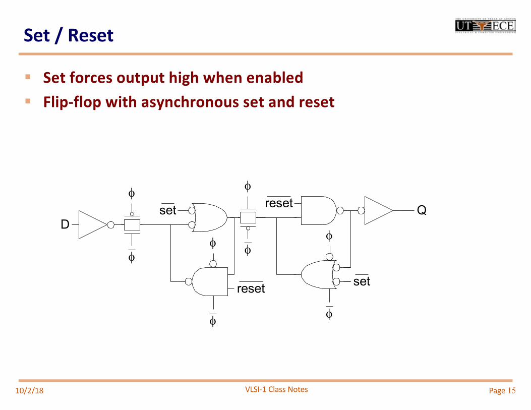
Set / Reset
§ Set forces output high when enabled§ Flip-flop with asynchronous set and reset
D
f
f
f
ff
f
Q
f
f
reset
set reset
set
10/2/18 Page 15
VLSI-1 Class Notes
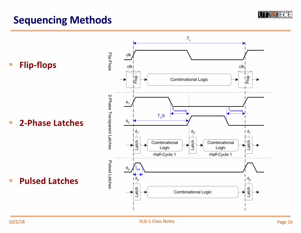
Sequencing Methods
10/2/18
§ Flip-flops
§ 2-Phase Latches
§ Pulsed LatchesFlip-Flops
Flop
Latc
h
Flop
clk
f1
f2
fp
clk clk
Latc
h
Latc
h
fp fp
f1 f1f2
2-Phase Transparent LatchesPulsed Latches
Combinational Logic
CombinationalLogic
CombinationalLogic
Combinational Logic
Latc
h
Latc
h
Tc
Tc/2tnonoverlap tnonoverlap
tpw
Half-Cycle 1 Half-Cycle 1
Page 16
VLSI-1 Class Notes
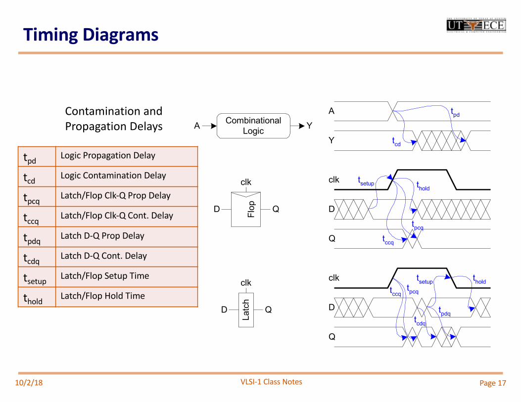
Timing Diagrams
10/2/18 Page 17
Flop
A
Y
tpdCombinational
LogicA Y
D Q
clk clk
D
QLatch
D Q
clk clk
D
Q
tcd
tsetup thold
tccq
tpcq
tccq
tsetup tholdtpcq
tpdqtcdq
tpd Logic Propagation Delay
tcd Logic Contamination Delay
tpcq Latch/Flop Clk-Q Prop Delay
tccq Latch/Flop Clk-Q Cont. Delay
tpdq Latch D-Q Prop Delay
tcdq Latch D-Q Cont. Delay
tsetup Latch/Flop Setup Time
thold Latch/Flop Hold Time
Contamination and Propagation Delays
VLSI-1 Class Notes
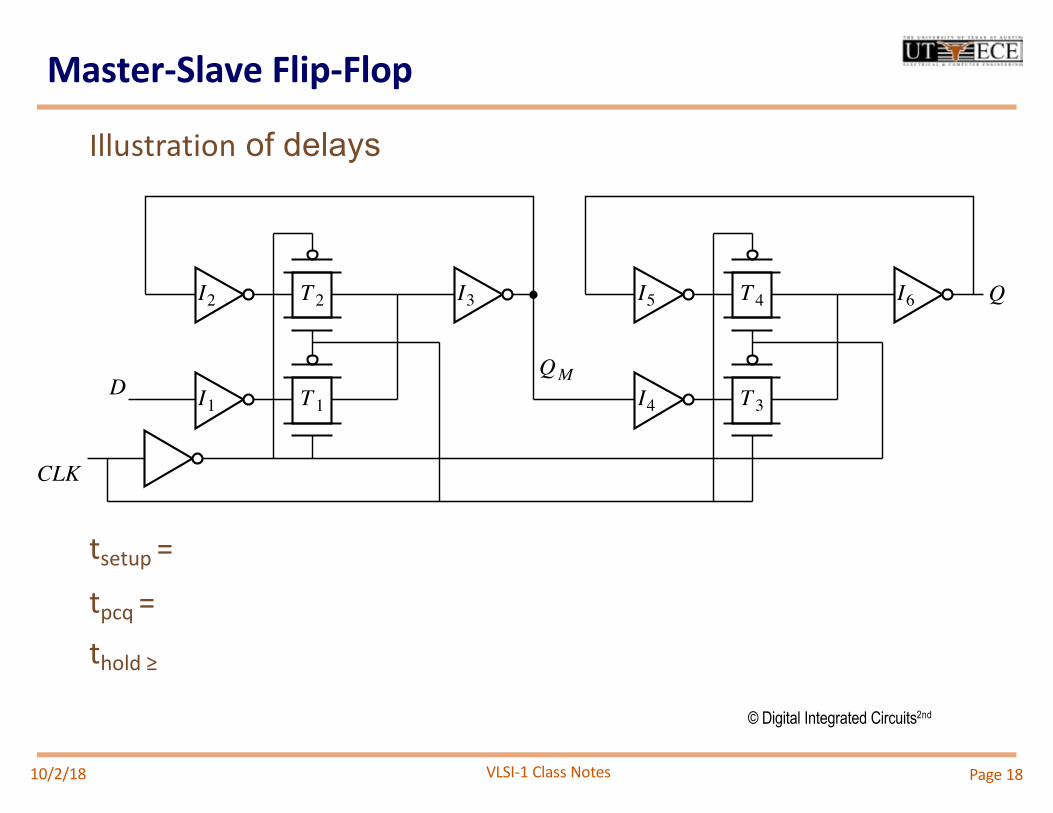
Master-Slave Flip-Flop
10/2/18
QM
Q
D
CLK
T2I2
T1I1
I3 T4I5
T3I4
I6
Illustration of delays
© Digital Integrated Circuits2nd
tsetup =tpcq =thold ≥
Page 18
VLSI-1 Class Notes
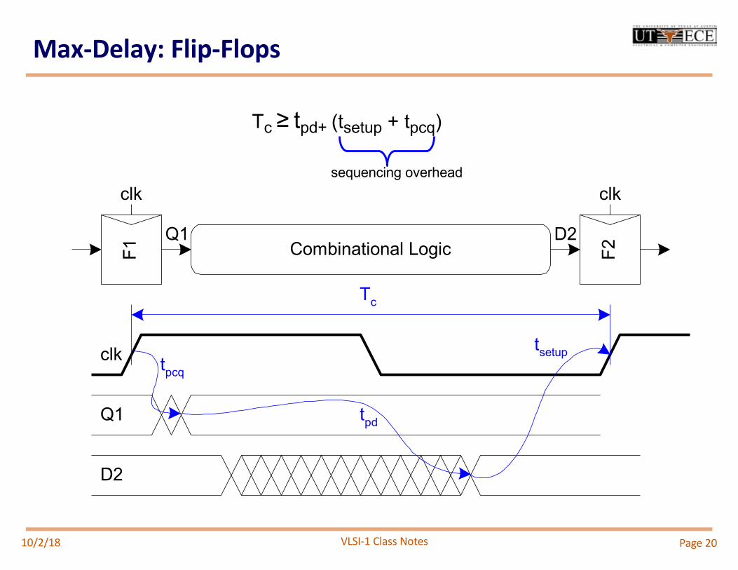
Max-Delay: Flip-Flops
10/2/18 Page 20
F1 F2
clk
clk clk
Combinational Logic
Tc
Q1 D2
Q1
D2
tpd
tsetuptpcq
Tc ≥ tpd+ (tsetup + tpcq)
sequencing overhead
VLSI-1 Class Notes
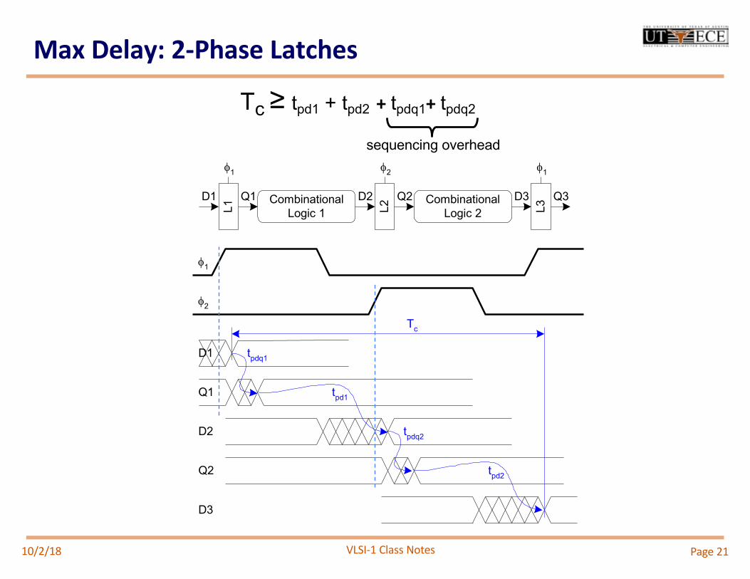
Max Delay: 2-Phase Latches
10/2/18
Tc
Q1
L1
f1
f2
L2 L3
f1 f1f2
CombinationalLogic 1
CombinationalLogic 2
Q2 Q3D1 D2 D3
Q1
D2
Q2
D3
D1
tpd1
tpdq1
tpd2
tpdq2
Tc ≥ tpd1 + tpd2 + tpdq1+ tpdq2
sequencing overhead
Page 21
VLSI-1 Class Notes
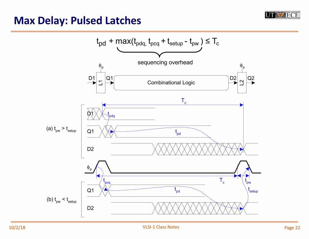
Max Delay: Pulsed Latches
Tc
Q1 Q2D1 D2
Q1
D2
D1
fp
fp fp
Combinational LogicL1 L2
tpw
(a) tpw > tsetup
Q1
D2(b) tpw < tsetup
Tc
tpd
tpdq
tpcq
tpd tsetup
tpd + max(tpdq, tpcq + tsetup - tpw ) ≤ Tc
sequencing overhead
10/2/18 Page 22
VLSI-1 Class Notes
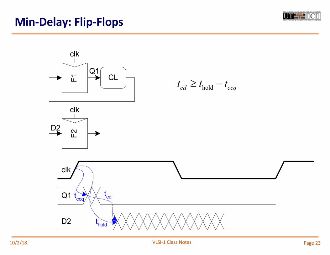
Min-Delay: Flip-Flops
holdcd ccqt t t³ -CL
clk
Q1
D2
F1
clk
Q1F2
clk
D2
tcd
thold
tccq
10/2/18 Page 23
VLSI-1 Class Notes
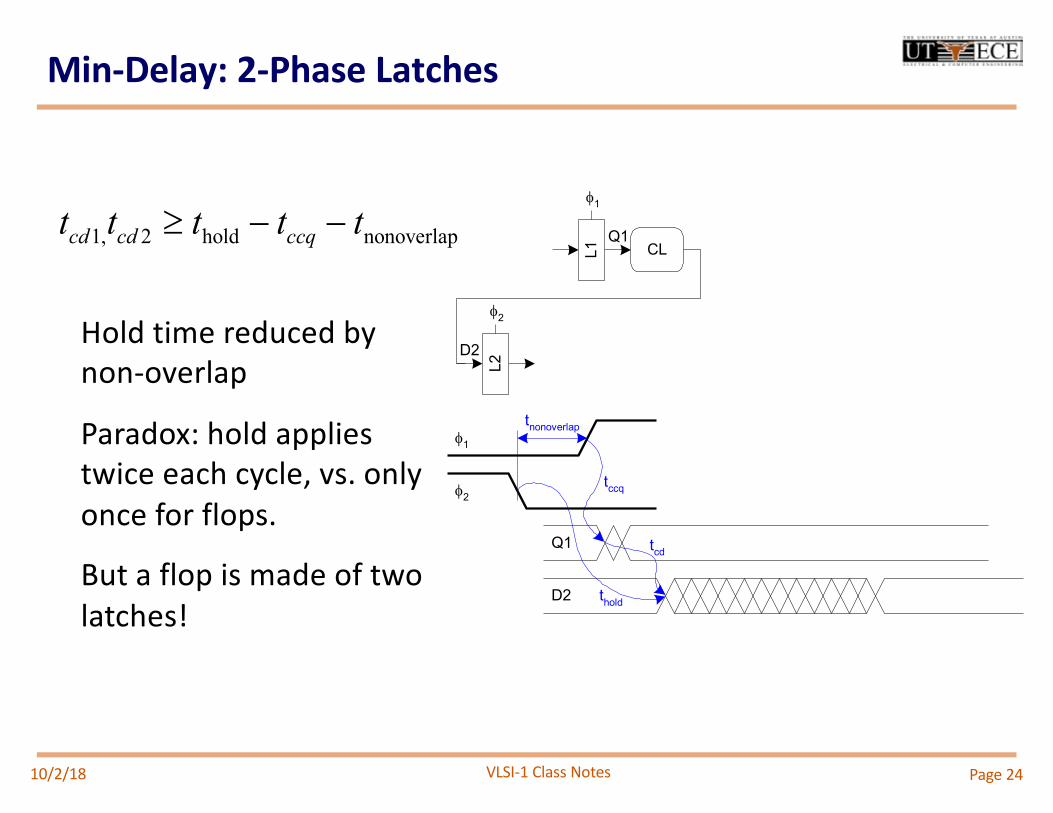
Min-Delay: 2-Phase Latches
1, 2 hold nonoverlapcd cd ccqt t t t t³ - -CL
Q1
D2
D2
Q1
f1
L1
f2
L2
f1
f2
tnonoverlap
tcd
thold
tccq
Hold time reduced by non-overlap
Paradox: hold applies twice each cycle, vs. only once for flops.
But a flop is made of two latches!
10/2/18 Page 24
VLSI-1 Class Notes
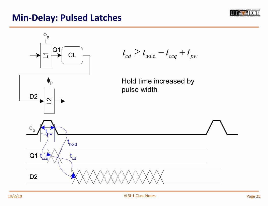
Min-Delay: Pulsed Latches
10/2/18
holdcd ccq pwt t t t³ - +CL
Q1
D2
Q1
D2
fp tpw
fpL1
fp
L2
tcd
thold
tccq
Hold time increased by pulse width
Page 25
VLSI-1 Class Notes
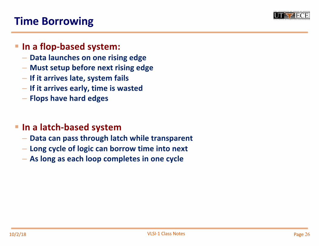
Time Borrowing
§ In a flop-based system:– Data launches on one rising edge– Must setup before next rising edge– If it arrives late, system fails– If it arrives early, time is wasted– Flops have hard edges
§ In a latch-based system– Data can pass through latch while transparent– Long cycle of logic can borrow time into next– As long as each loop completes in one cycle
10/2/18 Page 26
VLSI-1 Class Notes
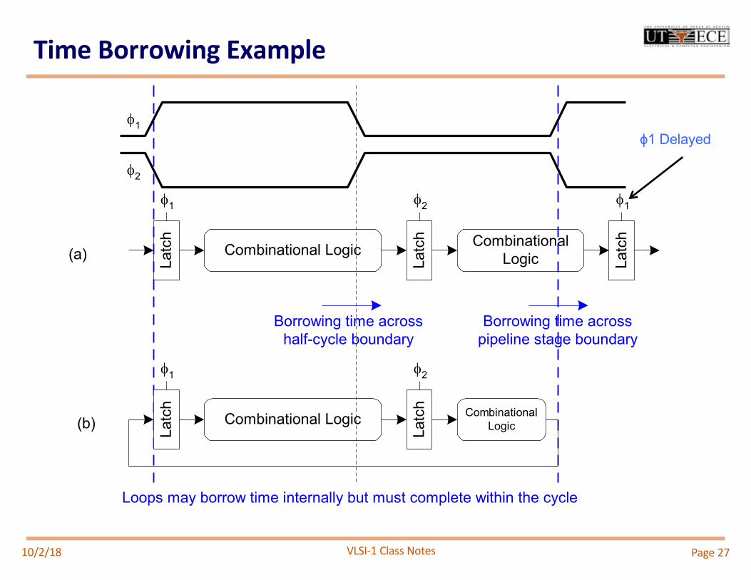
Time Borrowing Example
Latc
h
Latc
h
Latc
h
Combinational Logic CombinationalLogic
Borrowing time acrosshalf-cycle boundary
Borrowing time acrosspipeline stage boundary
(a)
(b) Latc
h
Latc
hCombinational Logic Combinational
Logic
Loops may borrow time internally but must complete within the cycle
f1
f2
f1 f1
f1
f2
f2
10/2/18 Page 27
ϕ1 Delayed
VLSI-1 Class Notes
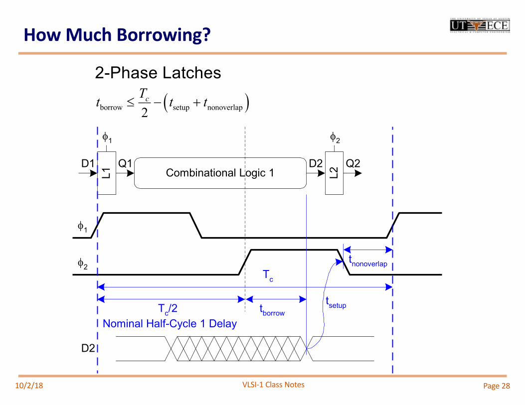
How Much Borrowing?
10/2/18
Q1
L1
f1
f2
L2
f1 f2
Combinational Logic 1Q2D1 D2
D2
Tc
Tc/2 Nominal Half-Cycle 1 Delay
tborrow
tnonoverlap
tsetup
( )borrow setup nonoverlap2cTt t t£ - +
2-Phase Latches
Page 28
VLSI-1 Class Notes
Clock Skew
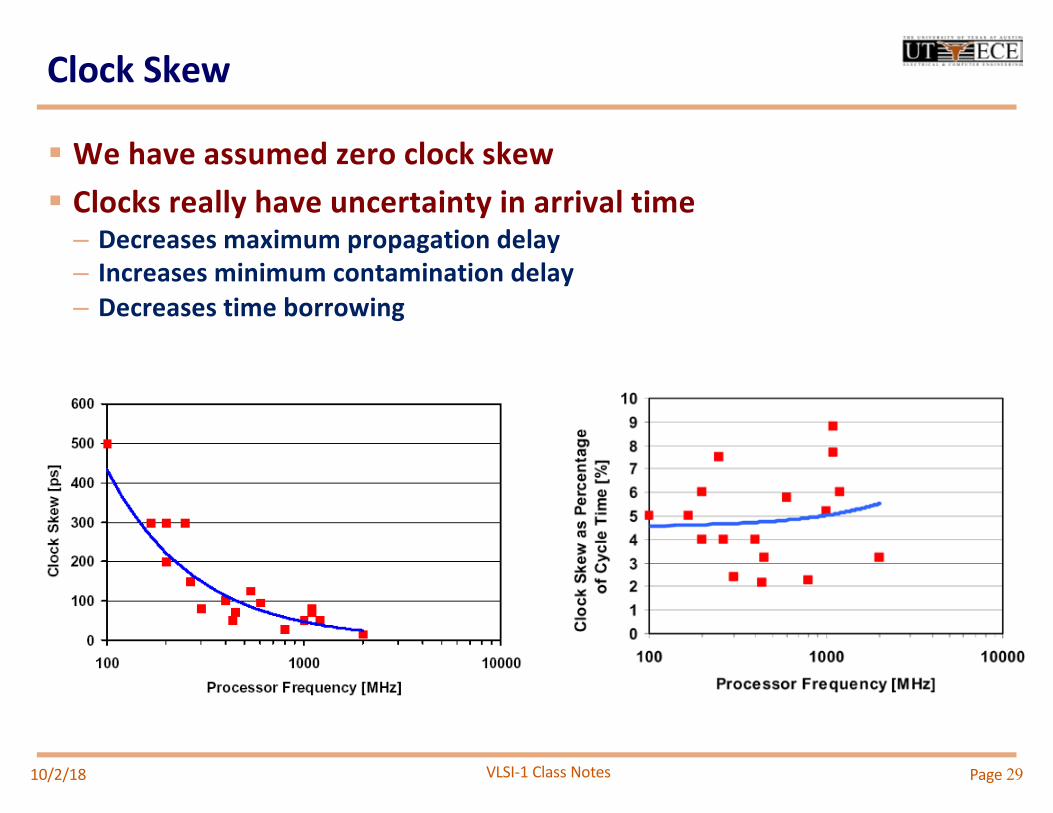
§ We have assumed zero clock skew§ Clocks really have uncertainty in arrival time– Decreases maximum propagation delay– Increases minimum contamination delay– Decreases time borrowing
10/2/18 Page 29
VLSI-1 Class Notes
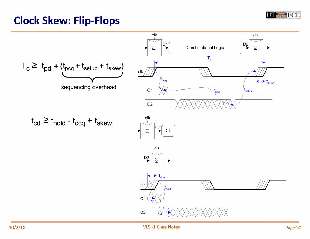
Clock Skew: Flip-Flops
10/2/18
F1 F2
clk
clk clk
Combinational Logic
Tc
Q1 D2
Q1
D2
tskew
CL
Q1
D2
F1
clk
Q1
F2
clk
D2
clk
tskew
tsetup
tpcq
tpdq
tcd
thold
tccq
Tc ≥ tpd + (tpcq + tsetup + tskew)
sequencing overhead
tcd ≥ thold - tccq + tskew
Page 30

VLSI-1 Class Notes
Clock Skew: Latches
10/2/18 31
Q1
L1
f1
f2
L2 L3
f1 f1f2
CombinationalLogic 1
CombinationalLogic 2
Q2 Q3D1 D2 D3
2-Phase Latches
Pulsed Latches
tpd ≤ Tc - (2tpdq)sequencing overhead
tcd1, tcd2 ≥ thold - tccq - tnonoverlap + tskew
tborrow ≤ Tc/2 - (tsetup + tnonoverlap + tskew)
tpd ≤ Tc - max(tpdq, tpcq + tsetup - tpw + tskew )
sequencing overhead
tcd ≥ thold + tpw - tccq + tskew
tborrow ≤ Tpw - (tsetup + tskew)
VLSI-1 Class Notes
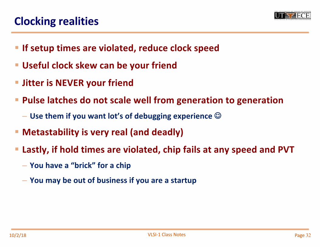
Clocking realities
§ If setup times are violated, reduce clock speed
§ Useful clock skew can be your friend
§ Jitter is NEVER your friend
§ Pulse latches do not scale well from generation to generation– Use them if you want lot’s of debugging experience JJ
§ Metastability is very real (and deadly)
§ Lastly, if hold times are violated, chip fails at any speed and PVT– You have a “brick” for a chip
– You may be out of business if you are a startup
10/2/18 Page 32
VLSI-1 Class Notes
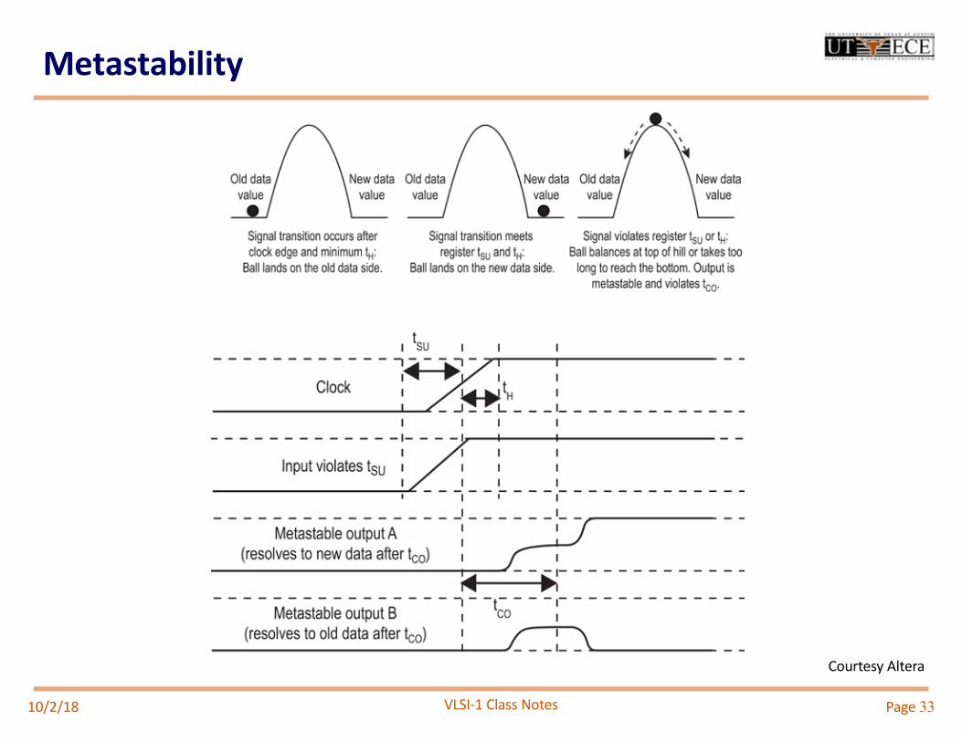
Metastability
Page 3310/2/18
Courtesy Altera
VLSI-1 Class Notes
Metastability - MTBF
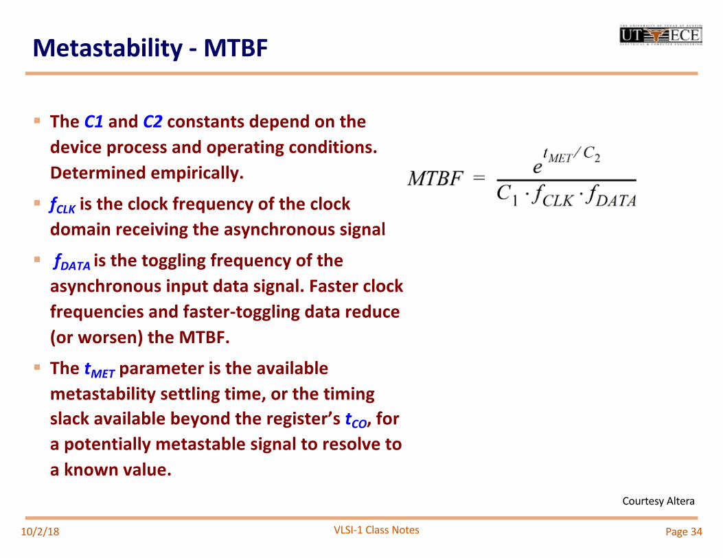
§ The C1 and C2 constants depend on the device process and operating conditions. Determined empirically.
§ fCLK is the clock frequency of the clock domain receiving the asynchronous signal
§ fDATA is the toggling frequency of the asynchronous input data signal. Faster clock frequencies and faster-toggling data reduce (or worsen) the MTBF.
§ The tMET parameter is the available metastability settling time, or the timing slack available beyond the register’s tCO, for a potentially metastable signal to resolve to a known value.
Page 3410/2/18
Courtesy Altera
VLSI-1 Class Notes
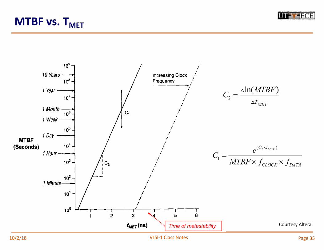
MTBF vs. TMET
2( )
1
METC t
CLOCK DATA
eCMTBF f f
´
=´ ´
2ln( )
MET
MTBFCt
=!!
Time of metastability Courtesy Altera
10/2/18 Page 35
VLSI-1 Class Notes
MTBF: Alternate definition
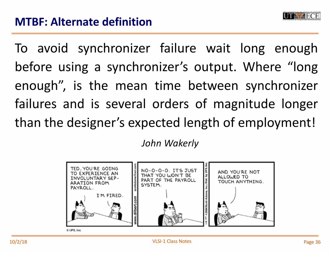
To avoid synchronizer failure wait long enoughbefore using a synchronizer’s output. Where “longenough”, is the mean time between synchronizerfailures and is several orders of magnitude longerthan the designer’s expected length of employment!
John Wakerly
10/2/18 Page 36
VLSI-1 Class Notes
Preventing Metastability
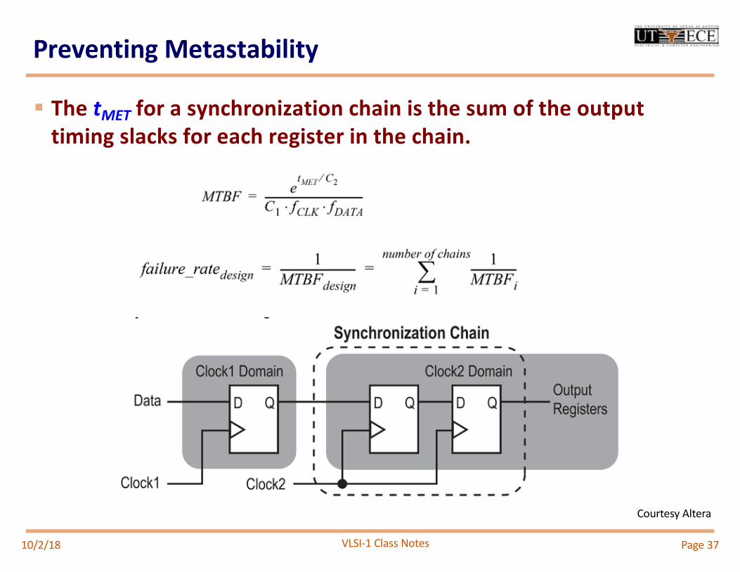
§ The tMET for a synchronization chain is the sum of the output timing slacks for each register in the chain.
Page 3710/2/18
Courtesy Altera
VLSI-1 Class Notes
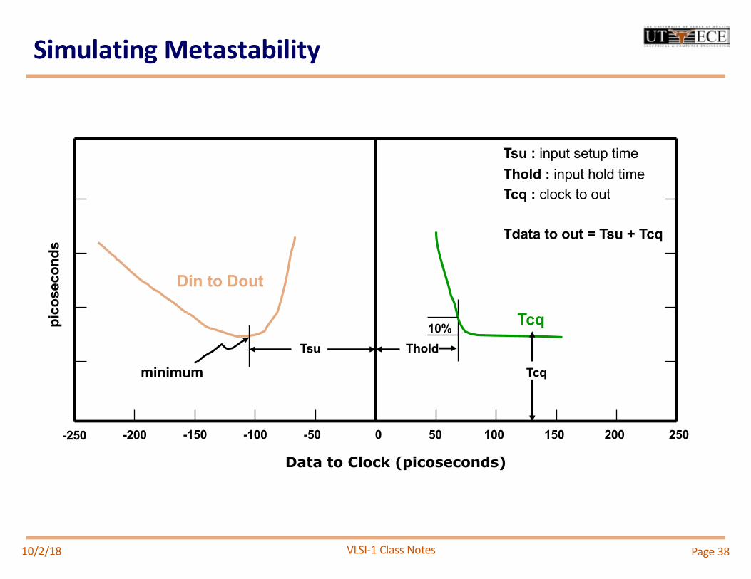
Simulating Metastability
10/2/18 Page 38
-200 -150 -100 -50 0 50 100 150 200 250
Data to Clock (picoseconds)
pico
seco
nds
-250
Tsu
Din to Dout
Thold
Tcq10%
minimum Tcq
Tsu : input setup timeThold : input hold timeTcq : clock to out
Tdata to out = Tsu + Tcq
VLSI-1 Class Notes
Din
Dout
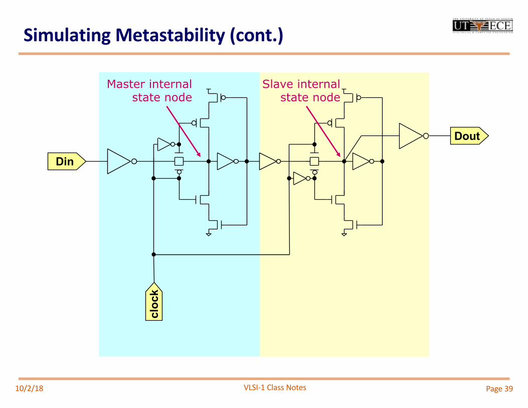
Simulating Metastability (cont.)
clock
10/2/18 Page 39
Master internal state node
Slave internal state node
VLSI-1 Class Notes
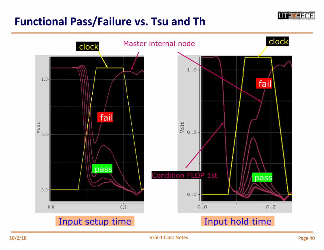
clock Master internal node
fail
pass
fail
pass
clock
Input setup time Input hold time
Condition FLOP 1st
Functional Pass/Failure vs. Tsu and Th
10/2/18 Page 40
VLSI-1 Class Notes
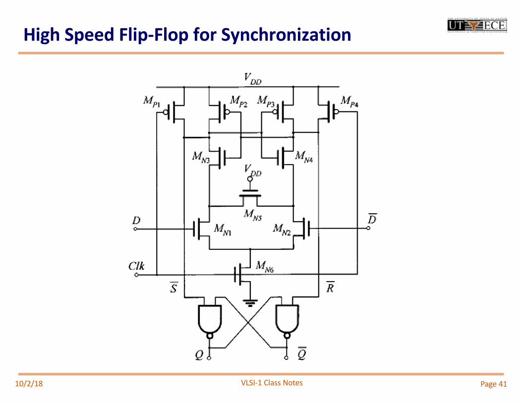
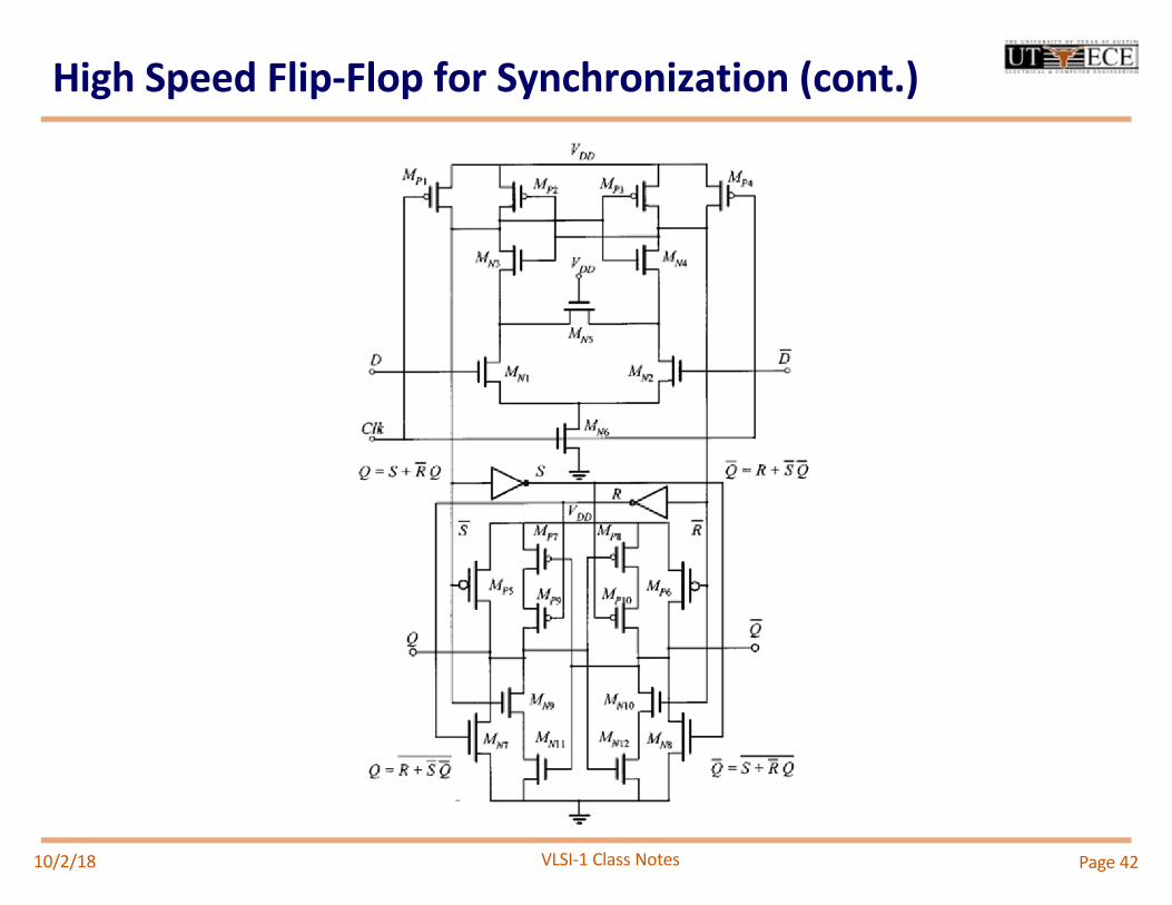
High Speed Flip-Flop for Synchronization
10/2/18 Page 41
VLSI-1 Class Notes
High Speed Flip-Flop for Synchronization (cont.)
10/2/18 Page 42
VLSI-1 Class Notes
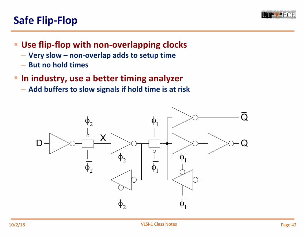
Safe Flip-Flop
§ Use flip-flop with non-overlapping clocks– Very slow – non-overlap adds to setup time– But no hold times
§ In industry, use a better timing analyzer– Add buffers to slow signals if hold time is at risk
10/2/18
D
f2
X
Q
Q
f1
f2
f1
f1f1
f2
f2
Page 43
VLSI-1 Class Notes
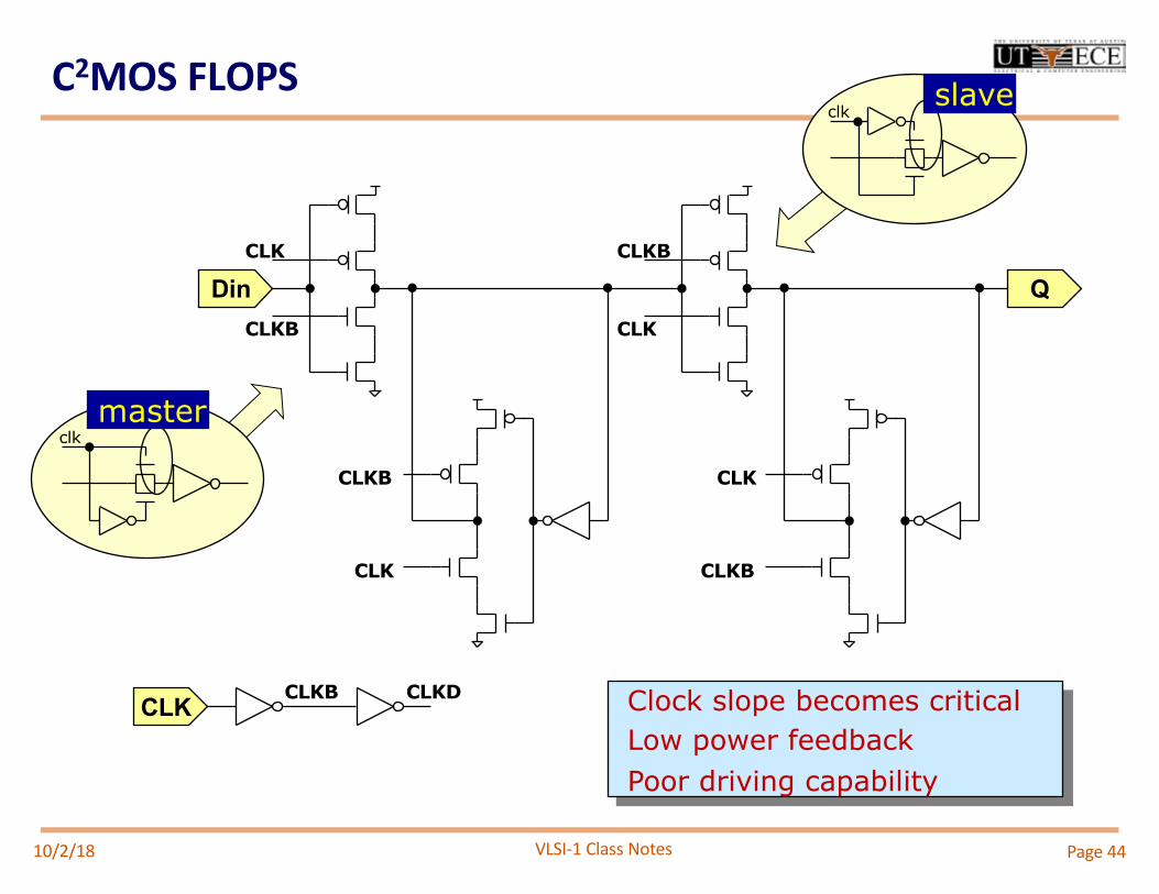
CLK
CLKB
CLKB
CLK
Din
CLKBCLK CLKD
Q
CLKB
CLK
CLK
CLKB
clk
clk
Clock slope becomes critical Low power feedbackPoor driving capability
master
slave C2MOS FLOPS
10/2/18 Page 44
VLSI-1 Class Notes
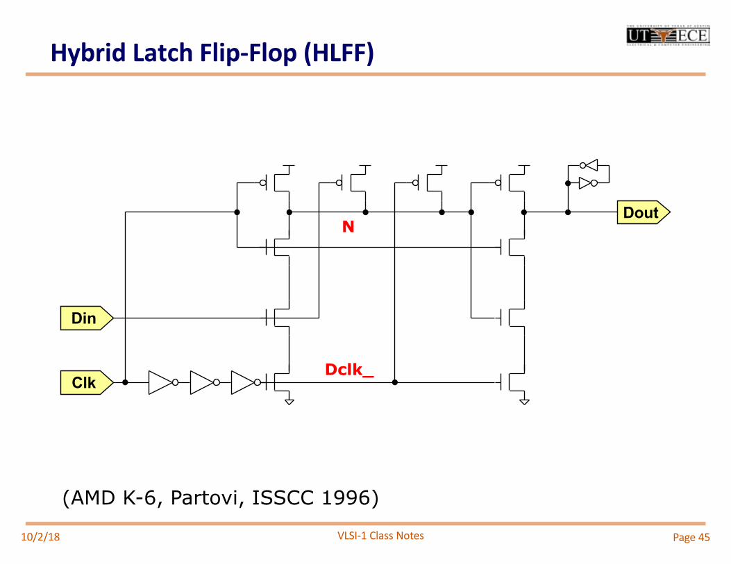
Hybrid Latch Flip-Flop (HLFF)
N
Dclk_
Din
Clk
Dout
(AMD K-6, Partovi, ISSCC 1996)
10/2/18 Page 45
VLSI-1 Class Notes
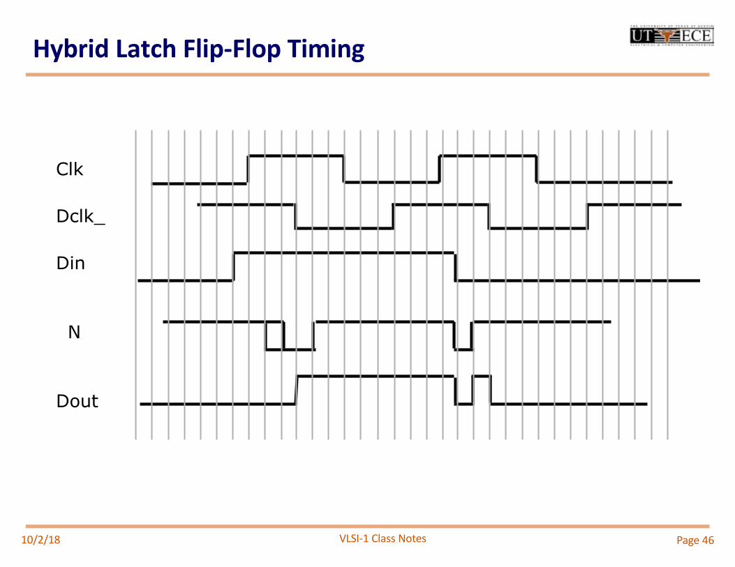
Hybrid Latch Flip-Flop Timing
10/2/18 Page 46
Clk
Dclk_
Din
N
Dout
!
!
VLSI-1 Class Notes
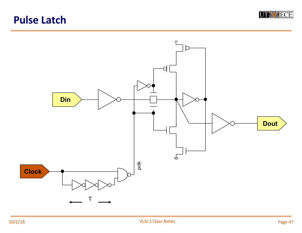
Din
Clock pclk
Dout
t
Pulse Latch
10/2/18 Page 47
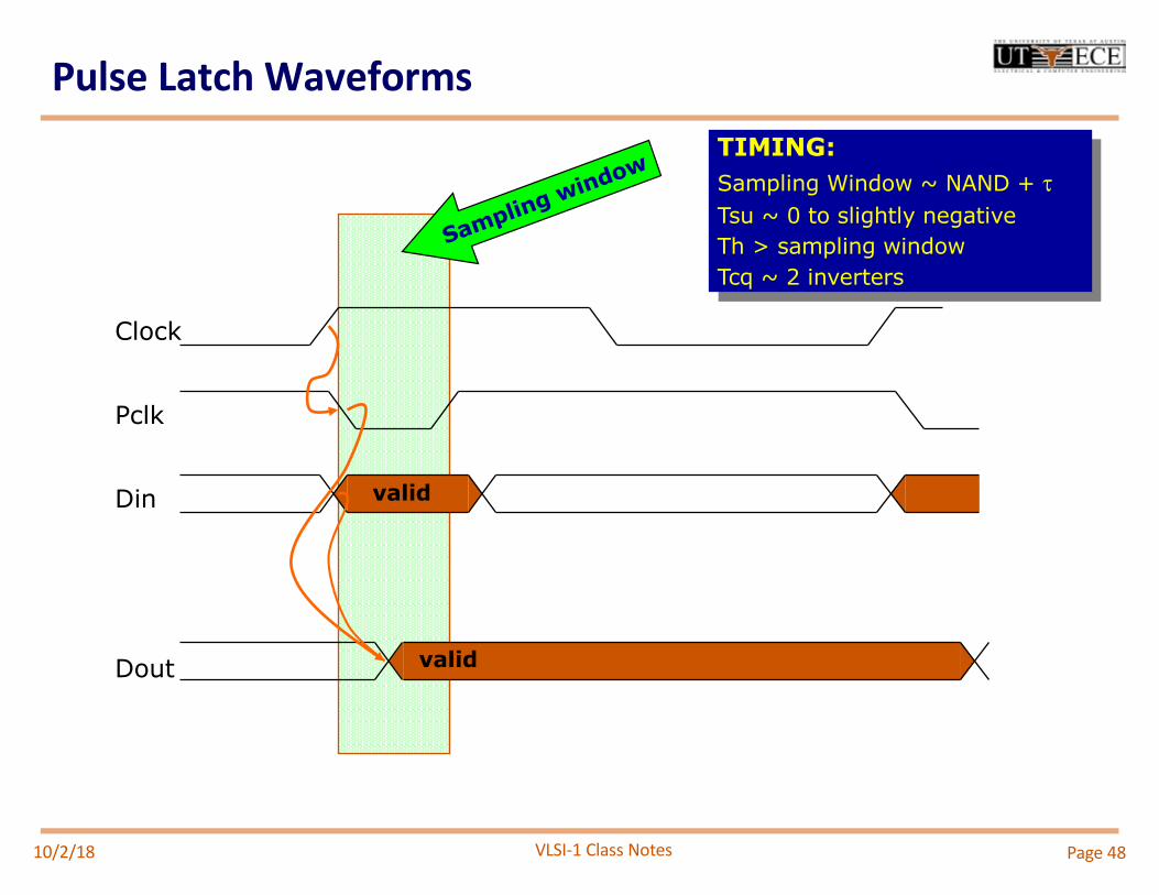
VLSI-1 Class Notes
Clock
Pclk
Din
Dout
valid
valid
Sampling windowTIMING:Sampling Window ~ NAND + tTsu ~ 0 to slightly negativeTh > sampling windowTcq ~ 2 inverters
Pulse Latch Waveforms
10/2/18 Page 48
VLSI-1 Class Notes •49
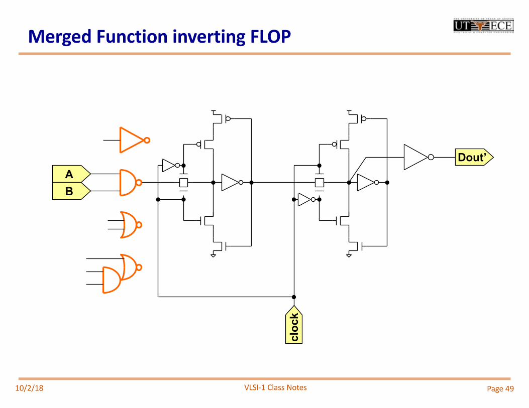
Merged Function inverting FLOP
clock
Dout’AB
10/2/18 Page 49
VLSI-1 Class Notes
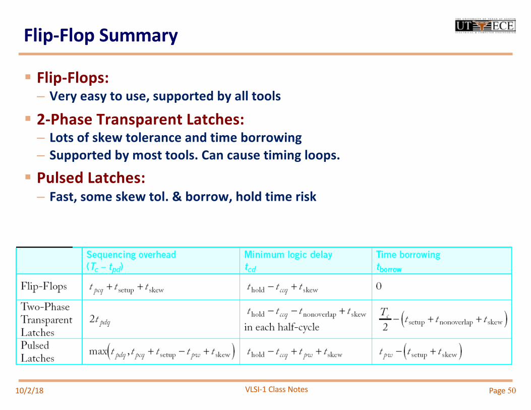
Flip-Flop Summary
§ Flip-Flops:– Very easy to use, supported by all tools
§ 2-Phase Transparent Latches:– Lots of skew tolerance and time borrowing– Supported by most tools. Can cause timing loops.
§ Pulsed Latches:– Fast, some skew tol. & borrow, hold time risk
10/2/18 Page 50

VLSI-1 Class Notes
Backup
10/2/18 Page 51
VLSI-1 Class Notes
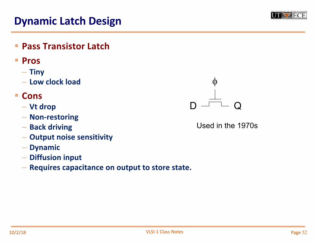
Dynamic Latch Design
§ Pass Transistor Latch§ Pros
– Tiny– Low clock load
§ Cons– Vt drop– Non-restoring– Back driving– Output noise sensitivity– Dynamic– Diffusion input– Requires capacitance on output to store state.
10/2/18
D Q
f
Used in the 1970s
Page 52
VLSI-1 Class Notes
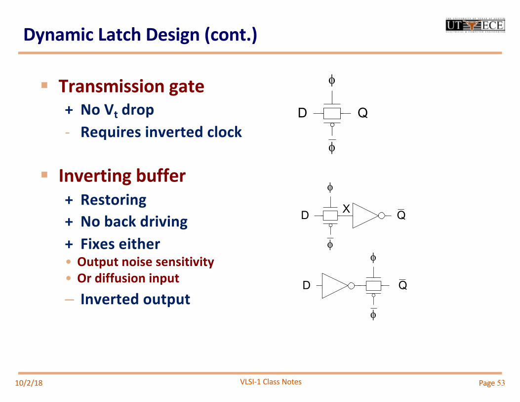
Dynamic Latch Design (cont.)
D
f
f
X Q
D Q
f
f
§ Transmission gate+ No Vt drop- Requires inverted clock
§ Inverting buffer+ Restoring+ No back driving+ Fixes either• Output noise sensitivity• Or diffusion input– Inverted output
D Q
f
f
10/2/18 Page 53