Module 1 Semiconductor (pn-Junction) Diodes Semiconductor (pn ...
PN junction and diodes
ELEC-H402/CH2: PN junction and diodes 1
Chapter 2
PN junction and diodes
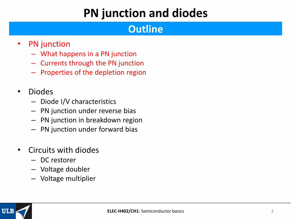
• PN junction– What happens in a PN junction– Currents through the PN junction– Properties of the depletion region
• Diodes– Diode I/V characteristics– PN junction under reverse bias– PN junction in breakdown region– PN junction under forward bias
• Circuits with diodes– DC restorer– Voltage doubler– Voltage multiplier
ELEC-H402/CH1: Semiconductor basics 2
Outline
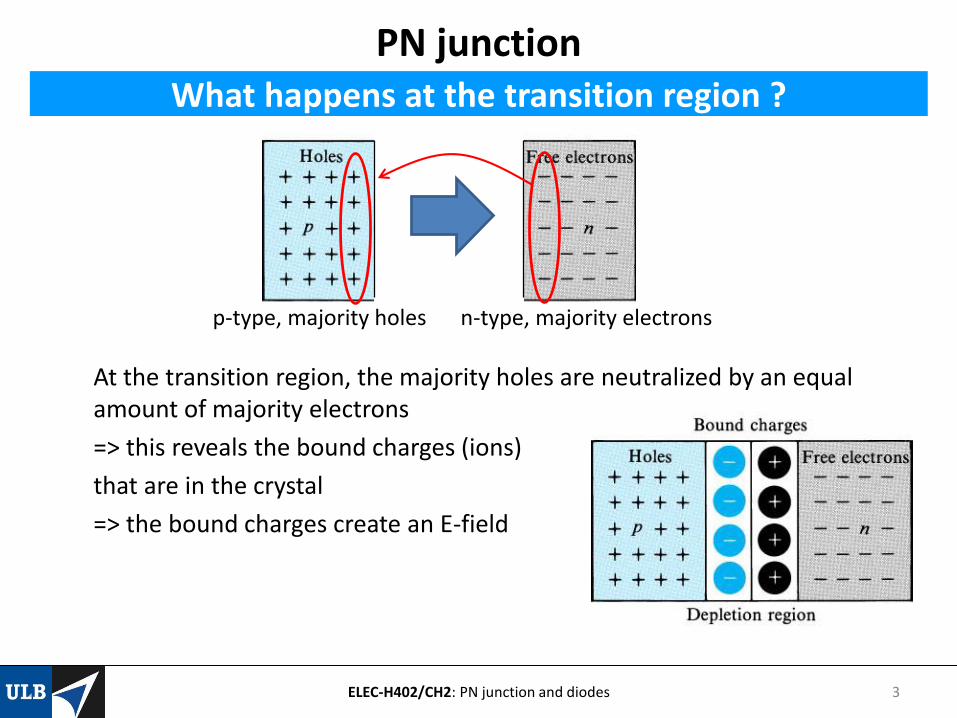
At the transition region, the majority holes are neutralized by an equalamount of majority electrons
=> this reveals the bound charges (ions)
that are in the crystal
=> the bound charges create an E-field
PN junction
ELEC-H402/CH2: PN junction and diodes 3
What happens at the transition region ?
p-type, majority holes n-type, majority electrons
PN junction
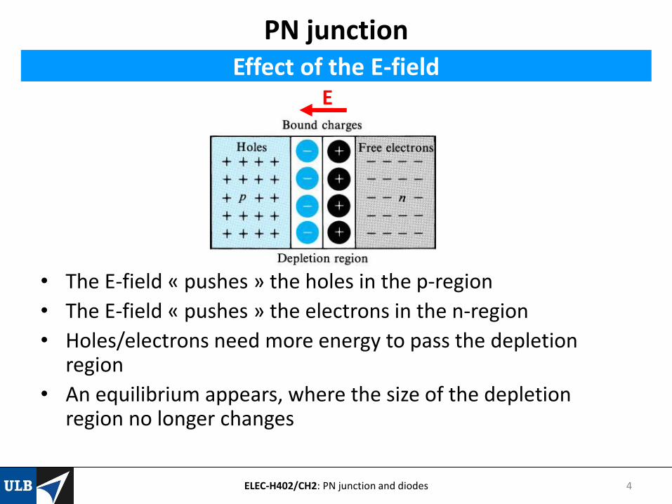
• The E-field « pushes » the holes in the p-region
• The E-field « pushes » the electrons in the n-region
• Holes/electrons need more energy to pass the depletionregion
• An equilibrium appears, where the size of the depletionregion no longer changes
ELEC-H402/CH2: PN junction and diodes 4
Effect of the E-fieldE
PN junction
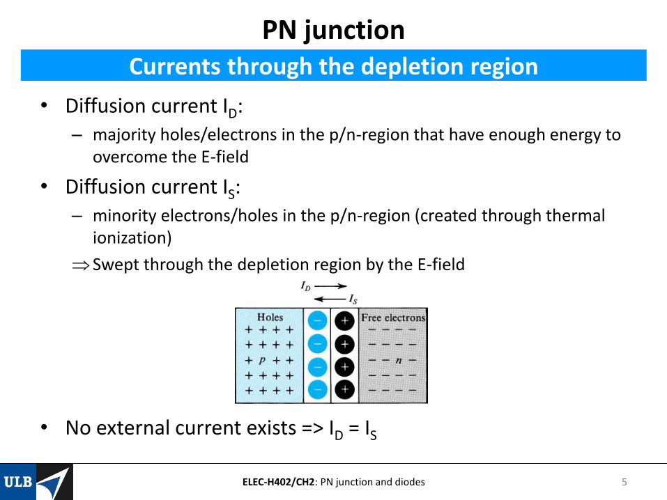
• Diffusion current ID:– majority holes/electrons in the p/n-region that have enough energy to
overcome the E-field
• Diffusion current IS: – minority electrons/holes in the p/n-region (created through thermal
ionization)
Swept through the depletion region by the E-field
• No external current exists => ID = IS
ELEC-H402/CH2: PN junction and diodes 5
Currents through the depletion region
PN junction
ELEC-H402/CH2: PN junction and diodes 6
Width and barrier voltage of the depletion region
x
x
E
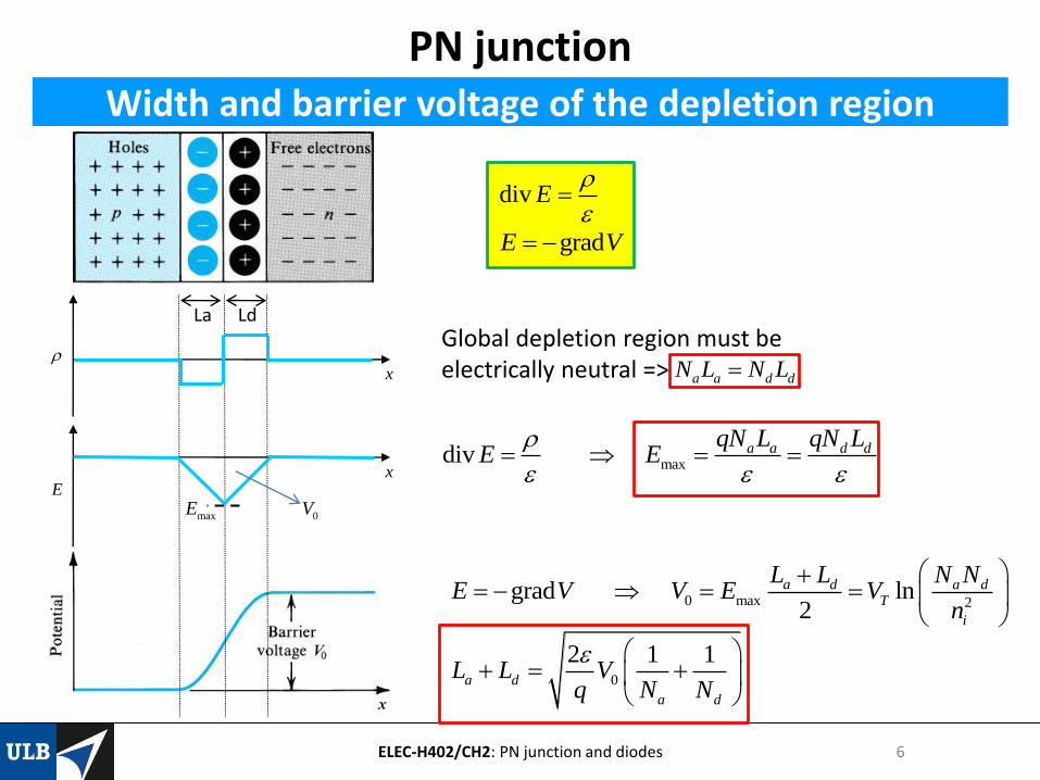
La LdGlobal depletion region must beelectrically neutral => a a d dN L N L
maxdiv a a d dqN L qN LE E
maxE
0 max 2grad ln
2
a d a dT
i
L L N NE V V E V
n
0
2 1 1a d
a d
L L Vq N N
div E
gradE V
0V
PN junction
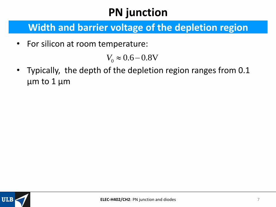
• For silicon at room temperature:
• Typically, the depth of the depletion region ranges from 0.1μm to 1 μm
ELEC-H402/CH2: PN junction and diodes 7
Width and barrier voltage of the depletion region
0 0.6 0.8VV
PN junction and diodes
• PN junction– What happens in a PN junction– Currents through the PN junction– Properties of the depletion region
• Diodes– Diode I/V characteristics– PN junction under reverse bias– PN junction in breakdown region– PN junction under forward bias
• Circuits with diodes– DC restorer– Voltage doubler– Voltage multiplier
ELEC-H402/CH1: Semiconductor basics 8
Outline
Diodes
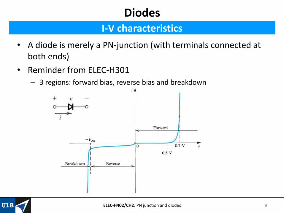
• A diode is merely a PN-junction (with terminals connected atboth ends)
• Reminder from ELEC-H301– 3 regions: forward bias, reverse bias and breakdown
ELEC-H402/CH2: PN junction and diodes 9
I-V characteristics
Diodes
ELEC-H402/CH2: PN junction and diodes 10
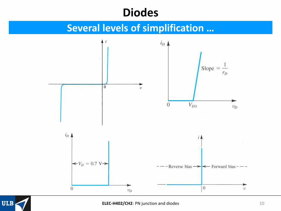
Several levels of simplification …
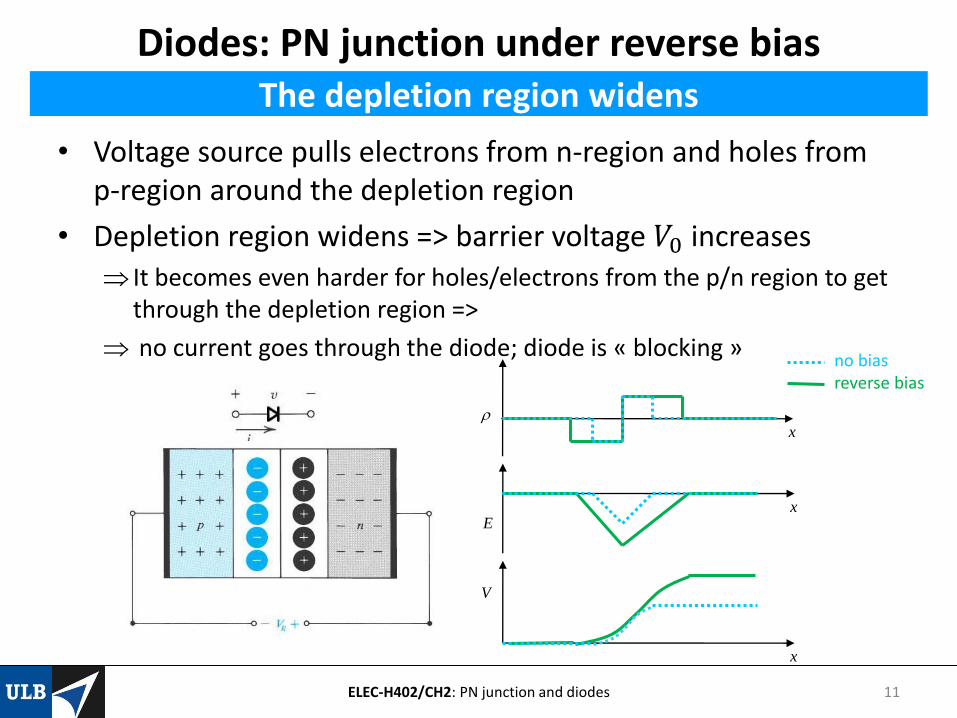
Diodes: PN junction under reverse bias
• Voltage source pulls electrons from n-region and holes fromp-region around the depletion region
• Depletion region widens => barrier voltage 𝑉0 increases It becomes even harder for holes/electrons from the p/n region to get
through the depletion region =>
no current goes through the diode; diode is « blocking »
ELEC-H402/CH2: PN junction and diodes 11
The depletion region widens
x
xE
x
V
no biasreverse bias
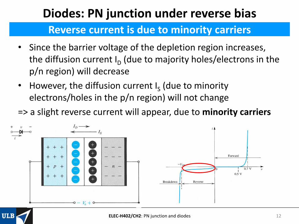
Diodes: PN junction under reverse bias
• Since the barrier voltage of the depletion region increases, the diffusion current ID (due to majority holes/electrons in the p/n region) will decrease
• However, the diffusion current IS (due to minorityelectrons/holes in the p/n region) will not change
=> a slight reverse current will appear, due to minority carriers
ELEC-H402/CH2: PN junction and diodes 12
Reverse current is due to minority carriers
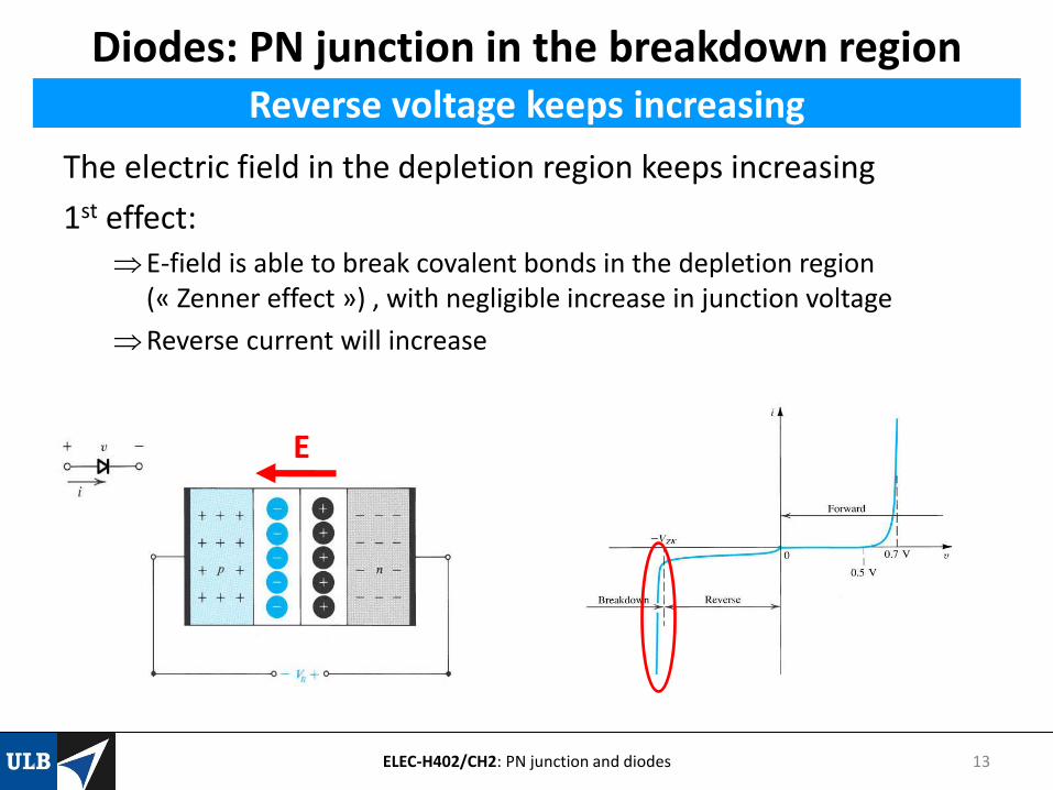
Diodes: PN junction in the breakdown region
The electric field in the depletion region keeps increasing
1st effect: E-field is able to break covalent bonds in the depletion region
(« Zenner effect ») , with negligible increase in junction voltage
Reverse current will increase
ELEC-H402/CH2: PN junction and diodes 13
Reverse voltage keeps increasing
E
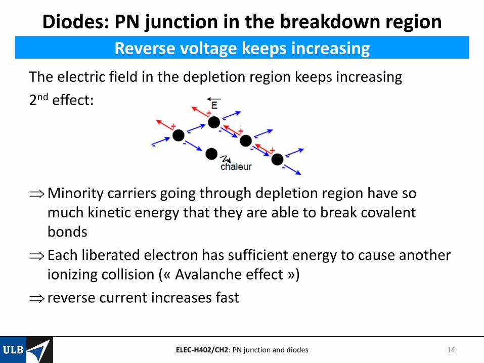
Diodes: PN junction in the breakdown region
The electric field in the depletion region keeps increasing
2nd effect:
Minority carriers going through depletion region have somuch kinetic energy that they are able to break covalent bonds
Each liberated electron has sufficient energy to cause anotherionizing collision (« Avalanche effect »)
reverse current increases fast
ELEC-H402/CH2: PN junction and diodes 14
Reverse voltage keeps increasing
Diodes: PN junction in the breakdown region
• When decreasing the reverse voltage, diode will return to itsoriginal state
However… reverse current can cause high power dissipation
This power dissipation can degrade the PN junctionirreversably, maybe even cause the Silicon to fuse
ELEC-H402/CH2: PN junction and diodes 15
PN breakdown is not a destructive process as such
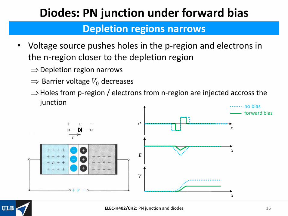
Diodes: PN junction under forward bias
• Voltage source pushes holes in the p-region and electrons in the n-region closer to the depletion regionDepletion region narrows
Barrier voltage 𝑉0 decreases
Holes from p-region / electrons from n-region are injected accross the junction
ELEC-H402/CH2: PN junction and diodes 16
Depletion regions narrows
x
xE
x
V
no biasforward bias
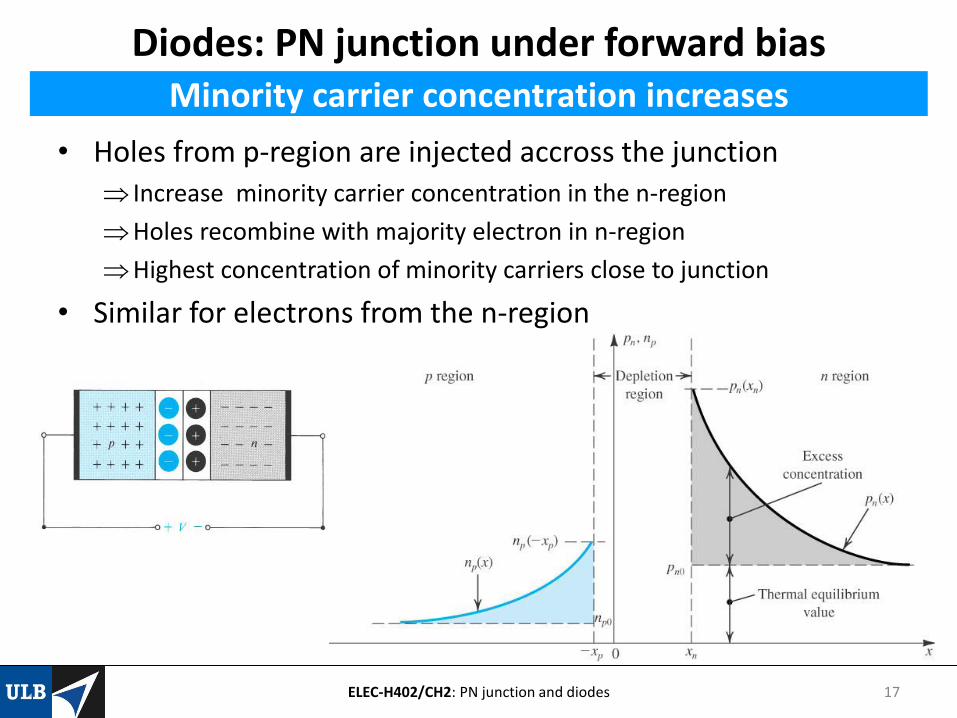
Diodes: PN junction under forward bias
• Holes from p-region are injected accross the junction Increase minority carrier concentration in the n-region
Holes recombine with majority electron in n-region
Highest concentration of minority carriers close to junction
• Similar for electrons from the n-region
ELEC-H402/CH2: PN junction and diodes 17
Minority carrier concentration increases
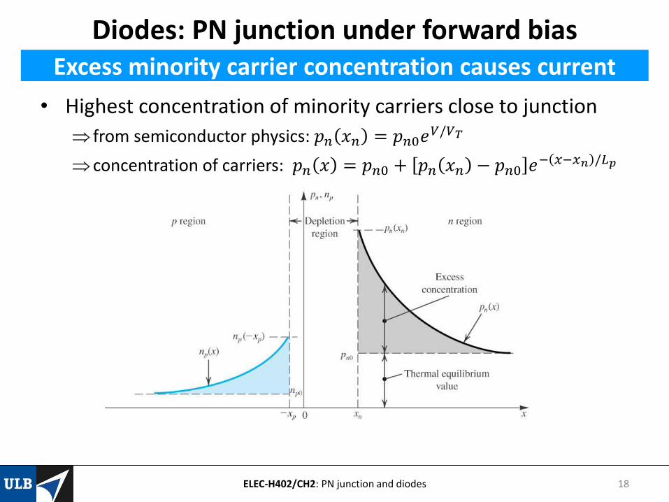
Diodes: PN junction under forward bias
• Highest concentration of minority carriers close to junction
from semiconductor physics: 𝑝𝑛 𝑥𝑛 = 𝑝𝑛0𝑒𝑉/𝑉𝑇
concentration of carriers: 𝑝𝑛 𝑥 = 𝑝𝑛0 + 𝑝𝑛 𝑥𝑛 − 𝑝𝑛0 𝑒− 𝑥−𝑥𝑛 /𝐿𝑝
ELEC-H402/CH2: PN junction and diodes 18
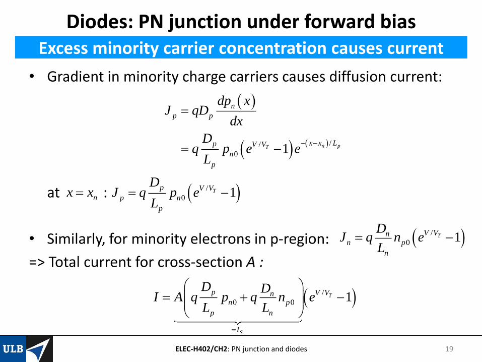
Excess minority carrier concentration causes current
Diodes: PN junction under forward bias
• Gradient in minority charge carriers causes diffusion current:
at :
• Similarly, for minority electrons in p-region:
=> Total current for cross-section A :
ELEC-H402/CH2: PN junction and diodes 19
Excess minority carrier concentration causes current
//
0 1 n pT
n
p p
x x Lp V V
n
p
dp xJ qD
dx
Dq p e e
L
/
0 1Tp V V
p n
p
DJ q p e
L nx x
/
0 1TV Vnn p
n
DJ q n e
L
/
0 0 1T
S
p V Vnn p
p n
I
D DI A q p q n e
L L
Diodes: PN junction under forward bias
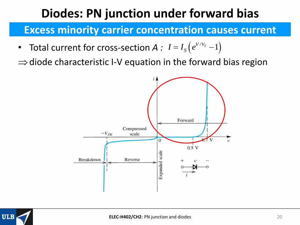
• Total current for cross-section A :
diode characteristic I-V equation in the forward bias region
ELEC-H402/CH2: PN junction and diodes 20
Excess minority carrier concentration causes current
/1TV V
SI I e
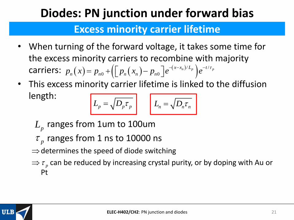
Diodes: PN junction under forward bias
• When turning of the forward voltage, it takes some time for the excess minority carriers to recombine with majoritycarriers:
• This excess minority carrier lifetime is linked to the diffusion length:
ranges from 1um to 100um
ranges from 1 ns to 10000 nsdetermines the speed of diode switching
can be reduced by increasing crystal purity, or by doping with Au or Pt
ELEC-H402/CH2: PN junction and diodes 21
Excess minority carrier lifetime
p p pL D
pL
p
p
/ /
0 0n p px x L t
n n n n np x p p x p e e
n n nL D
PN junctions: conclusions
• Forward bias– Depletion area narrows and more majority carriers cross junction
– Cause excess minority carriers
create diffusion current
Diffusion current exponential with forward voltage
• Reverse bias– Depletion area widens and less majority carriers cross junction
– Minority carriers still cross junction
IS (due to minority carriers) becomes larger than ID (due to majoritycarriers)
Small reverse current
ELEC-H402/CH2: PN junction and diodes 22
Summary
PN junctions: conclusions
• Breakdown region– Zenner effect: large E-field breaks covalent bonds
Large reverse current
– Large E-field: minority carriers have enough kinetic energy to break covalent bonds
Freed electrons also break other covalent bonds (Avalanche effect)
Large reverse current
ELEC-H402/CH2: PN junction and diodes 23
Summary
PN junction and diodes
• PN junction– What happens in a PN junction– Currents through the PN junction– Properties of the depletion region
• Diodes– Diode I/V characteristics– PN junction under reverse bias– PN junction in breakdown region– PN junction under forward bias
• Circuits with diodes– DC restorer– Voltage doubler– Voltage multiplier
ELEC-H402/CH1: Semiconductor basics 24
Outline
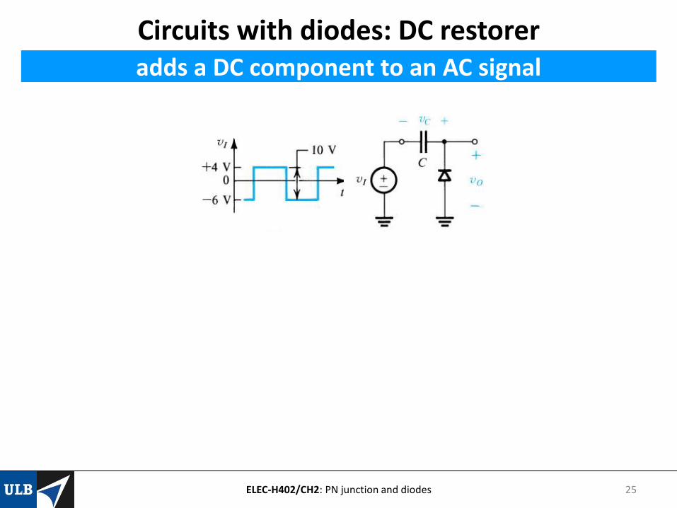
Circuits with diodes: DC restorer
ELEC-H402/CH2: PN junction and diodes 25
adds a DC component to an AC signal
Circuits with diodes: DC restorer
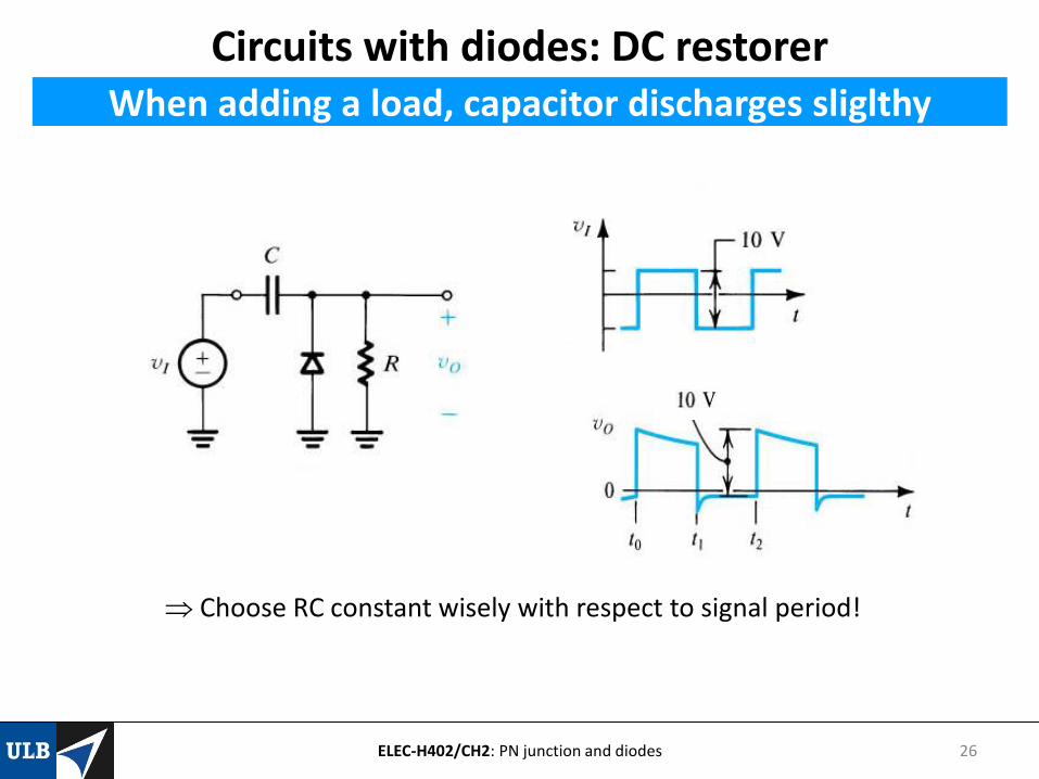
ELEC-H402/CH2: PN junction and diodes 26
When adding a load, capacitor discharges sliglthy
Choose RC constant wisely with respect to signal period!
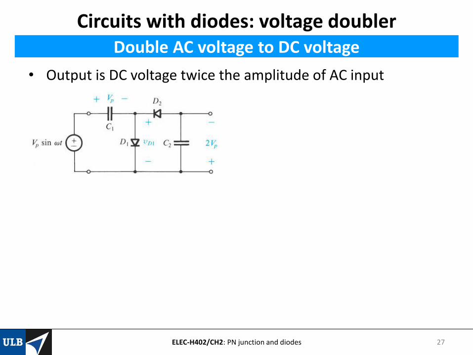
Circuits with diodes: voltage doubler
• Output is DC voltage twice the amplitude of AC input
ELEC-H402/CH2: PN junction and diodes 27
Double AC voltage to DC voltage
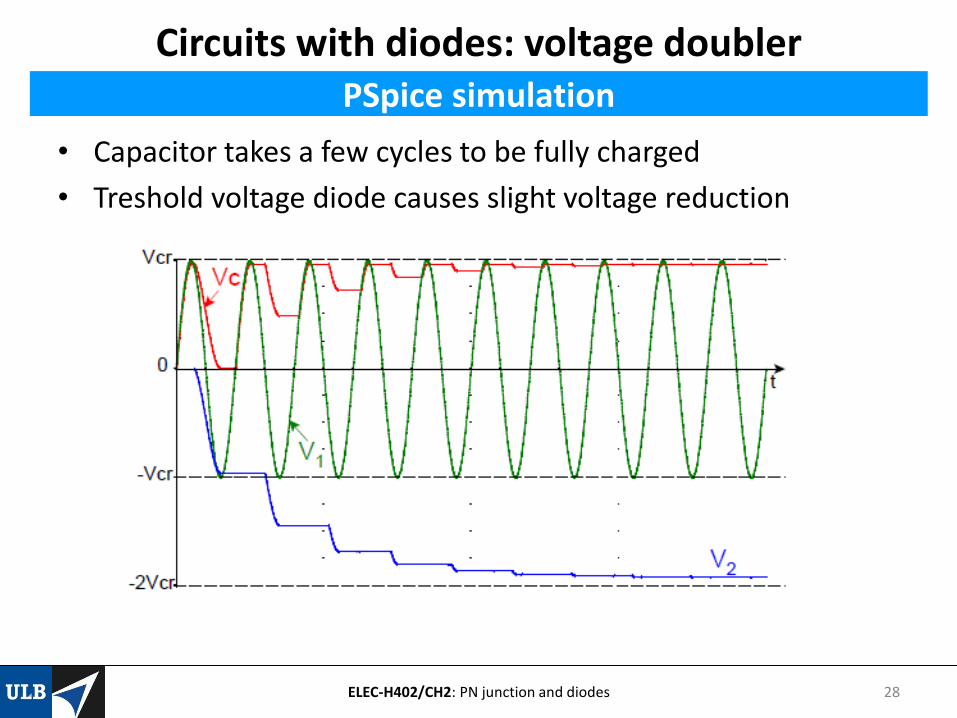
Circuits with diodes: voltage doubler
• Capacitor takes a few cycles to be fully charged
• Treshold voltage diode causes slight voltage reduction
ELEC-H402/CH2: PN junction and diodes 28
PSpice simulation
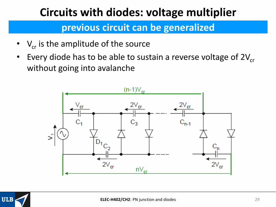
Circuits with diodes: voltage multiplier
• Vcr is the amplitude of the source
• Every diode has to be able to sustain a reverse voltage of 2Vcr
without going into avalanche
ELEC-H402/CH2: PN junction and diodes 29
previous circuit can be generalized