Chapter 1: Islamic University of Gaza Semiconductor Diodes...
24
Chapter 1: Semiconductor Diodes Islamic University of Gaza Dr. Talal Skaik
Transcript of Chapter 1: Islamic University of Gaza Semiconductor Diodes...

Chapter 1:
Semiconductor Diodes
Islamic University of Gaza
Dr. Talal Skaik

Copyright ©2009 by Pearson Education, Inc.
Upper Saddle River, New Jersey 07458 • All rights reserved.
Electronic Devices and Circuit Theory, 10/e Robert L. Boylestad and Louis Nashelsky
Semiconductor Materials: Ge, Si, and GaAs
2
• They fall into two classes : single crystal and compound
• Single crystal : Germanium (Ge) and silicon (Si).
• Compound : gallium arsenide (GaAs),
cadmium sulfide (CdS),
gallium nitride (GaN),
gallium arsenide phosphide (GaAsP)
Semiconductors are a special class of elements having a conductivity between that of a good conductor and that of an insulator.
The three semiconductors used most frequently in the construction of electronic devices are Ge, Si, and GaAs.

Copyright ©2009 by Pearson Education, Inc.
Upper Saddle River, New Jersey 07458 • All rights reserved.
Electronic Devices and Circuit Theory, 10/e Robert L. Boylestad and Louis Nashelsky
3
Group → 1 2 3 4 5 6 7 8 9 10 11 12 13 14 15 16 17 18
↓ Period
1 1
H
2
He
2 3
Li
4
Be
5
B
6
C
7
N
8
O
9
F
10
Ne
3
11
N
a
12
M
g
13
Al
14
Si
15
P
16
S
17
Cl
18
Ar
4 19
K
20
Ca
21
S
c
22
Ti
23
V
24
Cr
25
Mn
26
Fe
27
Co
28
Ni
29
Cu
30
Zn
31
Ga
32
Ge
33
As
34
Se
35
Br
36
Kr
5
37
R
b
38
Sr
39
Y
40
Zr
41
Nb
42
Mo
43
Tc
44
Ru
45
Rh
46
Pd
47
Ag
48
Cd
49
In
50
Sn
51
Sb
52
Te
53
I
54
Xe
6 55
Cs
56
Ba
*
72
Hf
73
Ta
74
W
75
Re
76
Os
77
Ir
78
Pt
79
Au
80
Hg
81
Tl
82
Pb
83
Bi
84
Po
85
At
86
Rn
7 87
Fr
88
Ra
**
104
Rf
105
Db
106
Sg
107
Bh
108
Hs
109
Mt
110
Ds
111
Rg
112
Uub
113
Uut
114
Uuq
115
Uup
116
Uuh
117
Uus
118
Uuo
* Lanthanides 57
La
58
Ce
59
Pr
60
Nd
61
Pm
62
Sm
63
Eu
64
Gd
65
Tb
66
Dy
67
Ho
68
Er
69
Tm
70
Yb
71
Lu
** Actinides 89
Ac
90
Th
91
Pa
92
U
93
Np
94
Pu
95
Am
96
Cm
97
Bk
98
Cf
99
Es
100
Fm
101
Md
102
No
103
Lr

Copyright ©2009 by Pearson Education, Inc.
Upper Saddle River, New Jersey 07458 • All rights reserved.
Electronic Devices and Circuit Theory, 10/e Robert L. Boylestad and Louis Nashelsky
History
4
• Diode , in 1939 was using Ge
• Transistor, in 1947 was using Ge
• In1954 Si was used in Transistor because Si is less
temperature sensitive and abundantly available.
• High speed transistor was using GaAs in 1970 (which is 5
times faster compared to Si)
• Si, Ge and GaAs are the semiconductor of choice
Copyright ©2009 by Pearson Education, Inc.
Upper Saddle River, New Jersey 07458 • All rights reserved.
Electronic Devices and Circuit Theory, 10/e Robert L. Boylestad and Louis Nashelsky
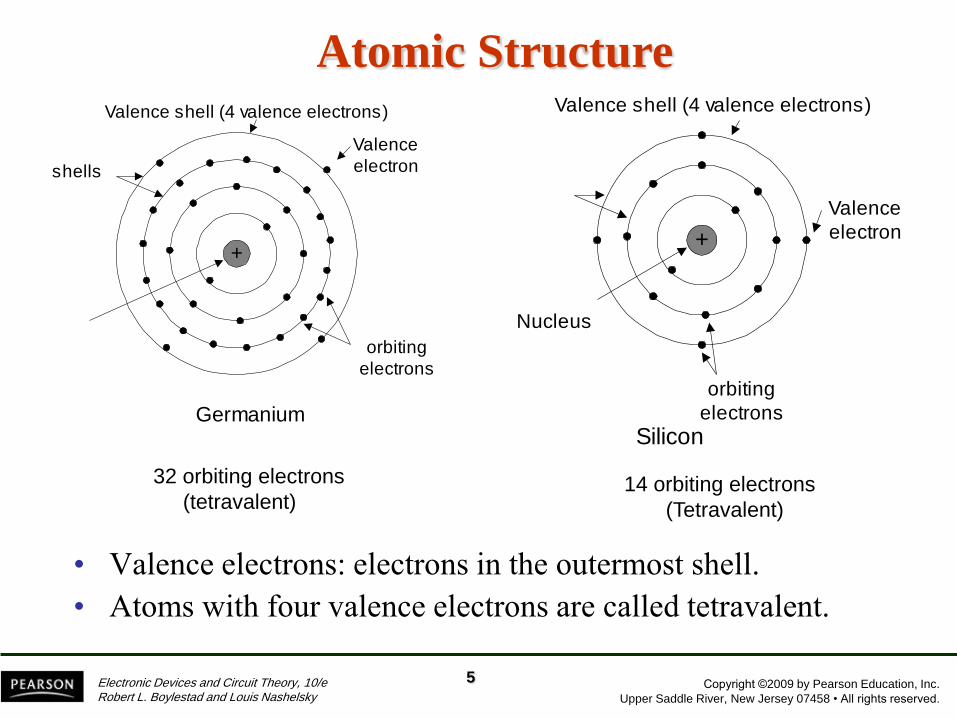
Atomic Structure
5
+
Valence shell (4 valence electrons)
Valence
electron
Nucleus
orbiting
electrons
Silicon
shells
+
Valence shell (4 valence electrons)
Valence
electron
orbiting
electrons
Germanium
14 orbiting electrons
(Tetravalent)
32 orbiting electrons
(tetravalent)
• Valence electrons: electrons in the outermost shell.
• Atoms with four valence electrons are called tetravalent.
Copyright ©2009 by Pearson Education, Inc.
Upper Saddle River, New Jersey 07458 • All rights reserved.
Electronic Devices and Circuit Theory, 10/e Robert L. Boylestad and Louis Nashelsky
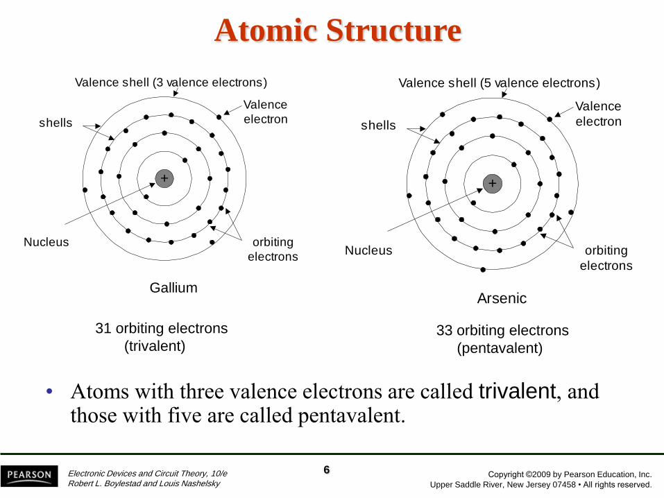
Atomic Structure
6
Nucleus
shells
+
Valence shell (3 valence electrons)
Valence
electron
orbiting
electrons
Gallium
Nucleus
shells
+
Valence shell (5 valence electrons)
Valence
electron
orbiting
electrons
Arsenic
31 orbiting electrons
(trivalent) 33 orbiting electrons
(pentavalent)
• Atoms with three valence electrons are called trivalent, and those with five are called pentavalent.

Copyright ©2009 by Pearson Education, Inc.
Upper Saddle River, New Jersey 07458 • All rights reserved.
Electronic Devices and Circuit Theory, 10/e Robert L. Boylestad and Louis Nashelsky
Covalent Bonding
7
This bonding of atoms, strengthened by the sharing of electrons,
is called covalent bonding
Covalent bonding of Si crystal

Copyright ©2009 by Pearson Education, Inc.
Upper Saddle River, New Jersey 07458 • All rights reserved.
Electronic Devices and Circuit Theory, 10/e Robert L. Boylestad and Louis Nashelsky
Covalent Bonding
8
Covalent bonding of GaAs crystal
There is sharing of
electrons, five electrons
provided by As atom and
three by the Ga atom.

Copyright ©2009 by Pearson Education, Inc.
Upper Saddle River, New Jersey 07458 • All rights reserved.
Electronic Devices and Circuit Theory, 10/e Robert L. Boylestad and Louis Nashelsky
9
Copyright ©2009 by Pearson Education, Inc.
Upper Saddle River, New Jersey 07458 • All rights reserved.
Electronic Devices and Circuit Theory, 10/e Robert L. Boylestad and Louis Nashelsky
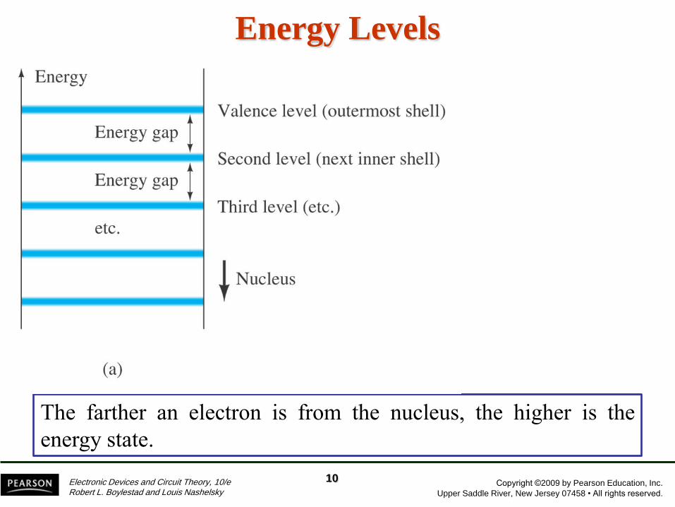
Energy Levels
10
The farther an electron is from the nucleus, the higher is the
energy state.

Copyright ©2009 by Pearson Education, Inc.
Upper Saddle River, New Jersey 07458 • All rights reserved.
Electronic Devices and Circuit Theory, 10/e Robert L. Boylestad and Louis Nashelsky
Energy Levels
11
An electron in the valence band of silicon must absorb more energy than
one in the valence band of germanium to become a free carrier. [free
carriers are free electrons due only to external causes such as applied
electric fields established by voltage sources or potential difference.

Copyright ©2009 by Pearson Education, Inc.
Upper Saddle River, New Jersey 07458 • All rights reserved.
Electronic Devices and Circuit Theory, 10/e Robert L. Boylestad and Louis Nashelsky
n-Type and p-Type materials
12
n-Type Material
Doping with Sb, (antimony)
n-Type materials are created by
adding elements with five valence
electrons such as antimony, arsenic,
and phosphorous.
There is a fifth electron due to
the (Sb) atom that is relatively free
to move in the n-Type material.
The atoms (in this case is
antimony (Sb)) are called donor
atoms.

Copyright ©2009 by Pearson Education, Inc.
Upper Saddle River, New Jersey 07458 • All rights reserved.
Electronic Devices and Circuit Theory, 10/e Robert L. Boylestad and Louis Nashelsky
n-Type and p-Type materials
13
n-Type Material
The free electrons due to the added atoms have higher energy
levels and require less energy to move to conduction band.

Copyright ©2009 by Pearson Education, Inc.
Upper Saddle River, New Jersey 07458 • All rights reserved.
Electronic Devices and Circuit Theory, 10/e Robert L. Boylestad and Louis Nashelsky
n-Type and p-Type materials
14
p-Type Material
Boron (B)
p-Type materials are created by
adding atoms with three valence
electrons such as boron, gallium, and
indium.
In this case, an insufficient
number of electrons to complete the
covalent bonds.
The resulting vacancy is called a
“hole” represented by small circle or
plus sign indicating absence of a
negative charge.
The atoms (in this case boron(B))
are called acceptor atoms.

Copyright ©2009 by Pearson Education, Inc.
Upper Saddle River, New Jersey 07458 • All rights reserved.
Electronic Devices and Circuit Theory, 10/e Robert L. Boylestad and Louis Nashelsky
Majority and Minority carriers
15
Two currents through a diode:
Majority Carriers
•The majority carriers in n-type materials are electrons.
•The majority carriers in p-type materials are holes.
Minority Carriers
•The minority carriers in n-type materials are holes.
•The minority carriers in p-type materials are electrons.

Copyright ©2009 by Pearson Education, Inc.
Upper Saddle River, New Jersey 07458 • All rights reserved.
Electronic Devices and Circuit Theory, 10/e Robert L. Boylestad and Louis Nashelsky
p-n Junctions
One end of a silicon or germanium crystal can be doped as a p-
type material and the other end as an n-type material.
The result is a p-n junction.
16

Copyright ©2009 by Pearson Education, Inc.
Upper Saddle River, New Jersey 07458 • All rights reserved.
Electronic Devices and Circuit Theory, 10/e Robert L. Boylestad and Louis Nashelsky
p-n Junctions At the p-n junction, the excess
conduction-band electrons on the
n-type side are attracted to the
valence-band holes on the p-type
side.
The electrons in the n-type
material migrate across the
junction to the p-type material
(electron flow).
The electron migration results in a
negative charge on the p-type side
of the junction and a positive
charge on the n-type side of the
junction.
The result is the formation of
a depletion region around
the junction.
17

Copyright ©2009 by Pearson Education, Inc.
Upper Saddle River, New Jersey 07458 • All rights reserved.
Electronic Devices and Circuit Theory, 10/e Robert L. Boylestad and Louis Nashelsky
Diodes
The diode is a 2-terminal device.
A diode ideally conducts in only
one direction.
18

Copyright ©2009 by Pearson Education, Inc.
Upper Saddle River, New Jersey 07458 • All rights reserved.
Electronic Devices and Circuit Theory, 10/e Robert L. Boylestad and Louis Nashelsky
Diode Operating Conditions • No bias
• Forward bias
• Reverse bias
19
Reverse bias Forward bias

Copyright ©2009 by Pearson Education, Inc.
Upper Saddle River, New Jersey 07458 • All rights reserved.
Electronic Devices and Circuit Theory, 10/e Robert L. Boylestad and Louis Nashelsky
Diode Operating Conditions
• No external voltage is applied: VD = 0 V
• No current is flowing: ID = 0 A
• Only a modest depletion region exists
20
No Bias
Copyright ©2009 by Pearson Education, Inc.
Upper Saddle River, New Jersey 07458 • All rights reserved.
Electronic Devices and Circuit Theory, 10/e Robert L. Boylestad and Louis Nashelsky
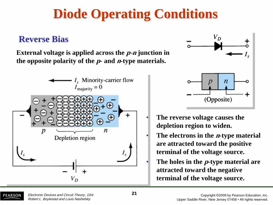
External voltage is applied across the p-n junction in
the opposite polarity of the p- and n-type materials.
Diode Operating Conditions
Reverse Bias
• The reverse voltage causes the
depletion region to widen.
• The electrons in the n-type material
are attracted toward the positive
terminal of the voltage source.
• The holes in the p-type material are
attracted toward the negative
terminal of the voltage source.
21

Copyright ©2009 by Pearson Education, Inc.
Upper Saddle River, New Jersey 07458 • All rights reserved.
Electronic Devices and Circuit Theory, 10/e Robert L. Boylestad and Louis Nashelsky
Diode Operating Conditions
Forward Bias
External voltage is applied across the p-n junction in
the same polarity as the p- and n-type materials.
• The forward voltage causes the
depletion region to narrow.
• The electrons and holes are pushed
toward the p-n junction.
• The electrons and holes have
sufficient energy to cross the p-n
junction.
22

Copyright ©2009 by Pearson Education, Inc.
Upper Saddle River, New Jersey 07458 • All rights reserved.
Electronic Devices and Circuit Theory, 10/e Robert L. Boylestad and Louis Nashelsky
Actual Diode Characteristics
Note the regions for no
bias, reverse bias, and
forward bias conditions.
Carefully note the scale
for each of these
conditions.
The reverse saturation
current is seldom more
than a few microamperes.
23

Copyright ©2009 by Pearson Education, Inc.
Upper Saddle River, New Jersey 07458 • All rights reserved.
Electronic Devices and Circuit Theory, 10/e Robert L. Boylestad and Louis Nashelsky
Diode equation
24
where
VT : is called the thermal voltage.
Is : is the reverse saturation current.
VD : is the applied forward-bias voltage across the diode.
n : is a factor function of operation conditions and physical
construction. It has range between 1 and 2. assume n=1 unless
otherwise noted.
K : is Boltzman’s constant =1.38 x 10⁻²³
T: is temperature in kelvins = 273+temperature in C.
q : is the magnitude of electron charge = 1.6 x 10⁻¹⁹ C.


![Semiconductor Diodes [Demo]](https://static.fdocuments.in/doc/165x107/577d294d1a28ab4e1ea66956/semiconductor-diodes-demo.jpg)