4.2 semiconductor diodes
21
PHYSIC FORM 5 CHAPTER 4: ELECTRONICS 4.2 SEMICONDUCTOR DIODES NAME : CLASS :
-
Upload
poppin-dragon -
Category
Education
-
view
43 -
download
0
Transcript of 4.2 semiconductor diodes
PHYSIC FORM 5 CHAPTER 4: ELECTRONICS 4.2 SEMICONDUCTOR DIODES
NAME :
CLASS :
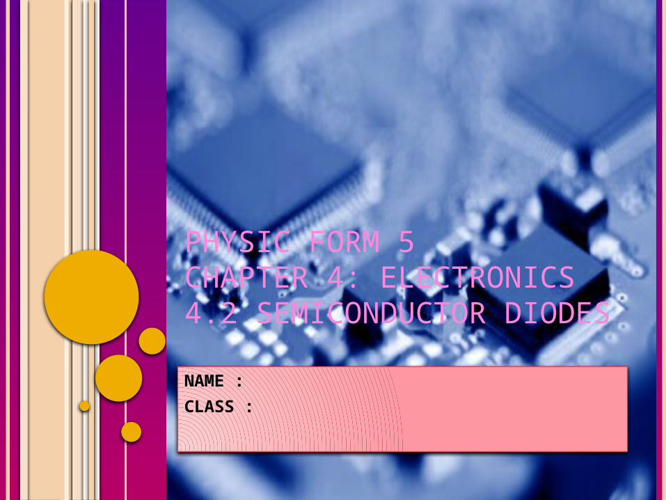
PROPERTIES OF SEMICONDUCTORS
Conductors are materials which allow current to flow through
them easily.
Reason : conductors have free electrons which can drift
between their atoms. Hence, conductors have low resistance.
Semiconductors are a group of materials that can conduct
better than insulators but not as good as metal conductors
Semiconductors can be pure element such as silicon,
germanium, boron, tellurium.
At 0 Kelvin it behaves as an insulator. When the temperature
increases, the conductivity of the electricity will increase
because its resistance will be lowered.
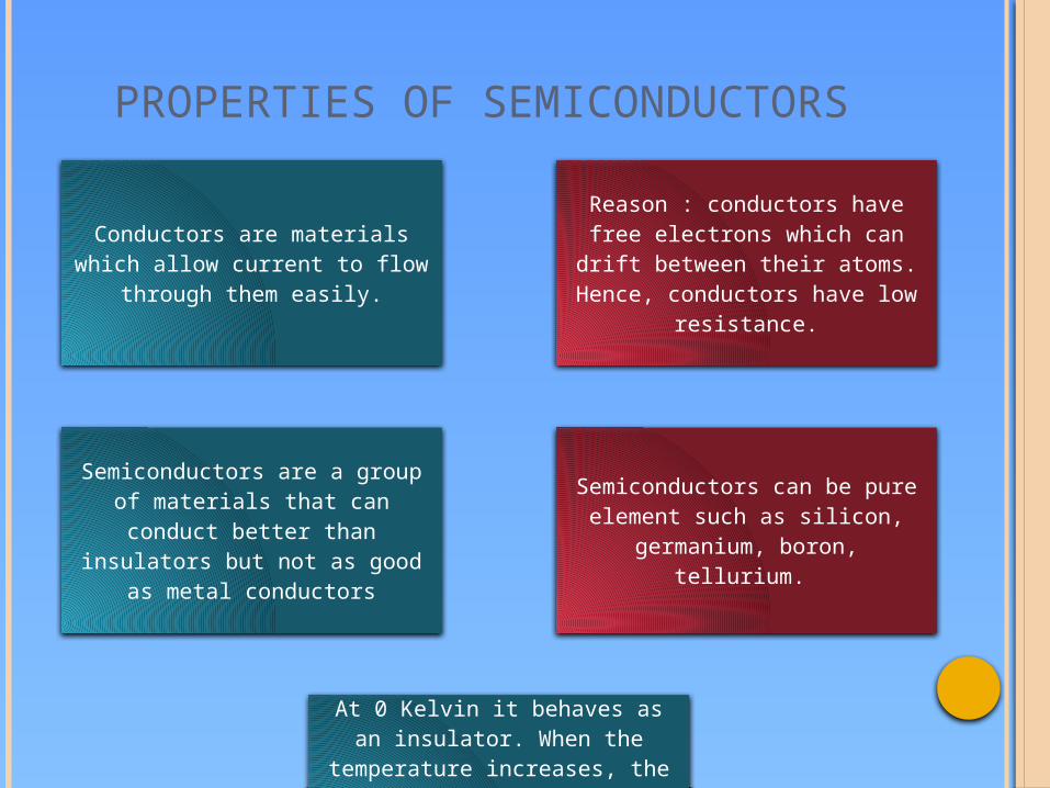
IN TERMS OF RESISTANCE
METALS INSULATORS
Good conductors of electricity because they have free electrons that can move easily between atoms
The resistance of metals is generally very low.
Poor conductors of electricity because they have too few free electrons to move about.
The resistance of insulators is very high
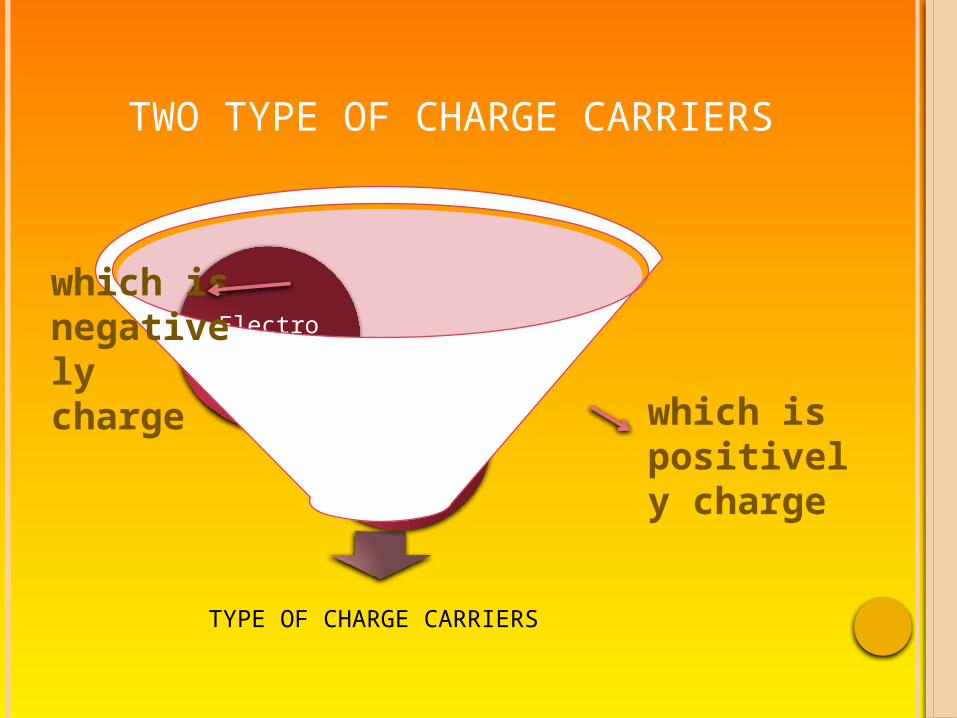
TWO TYPE OF CHARGE CARRIERS
TYPE OF CHARGE CARRIERS
Hole
Electron
which is negatively charge
which is positively charge

CHARACTERISTICS OF A SILICON ATOM
Figure on the top shows the outer electrons in a silicon crystal which all are involved in perfect covalent bonds, leaving no free electrons to conduct electricity.
There are four electrons in the outermost shell of a silicon atom and they are shared between four other neighbouring atoms to form four covalent bonds.
Each of the covalent bonds has a pair of electrons. Every atoms shares one electron with each of its neighbours.
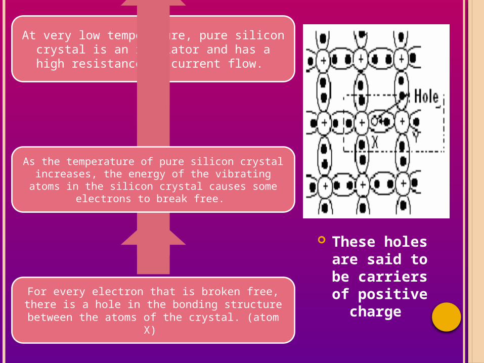
These holes are said to be carriers of positive
charge
At very low temperature, pure silicon crystal is an insulator and has a high
resistance to current flow.
As the temperature of pure silicon crystal increases, the energy of the vibrating atoms
in the silicon crystal causes some electrons to break free.
For every electron that is broken free, there is a hole in the bonding structure
between the atoms of the crystal. (atom X)

One outer electron from the neighbouring atom (Y) will fill the hole and at the same time will produce a hole at Y.
When the valence/outer electron moves to the left, the hole ‘move’ to the right
This is the physical origin of the increase in the electrical conductivity of semiconductors with temperature

Doping is a process of adding a small amount of impurities into the crystalline lattice of semiconductors to increase their conductivity.
Atoms of the impurities added should have almost the same size as the atoms of the semiconductors.
2 types of semiconductors can be obtained : p-type semiconductor n-type semiconductor
DOPING
Similarities
Undergoes the ‘doping’ process
Made from pure silicon or
germanium
Has electrons and holes as
charge carriers

Boron, indium, gallium, aluminium
Doping substance Antimony, arsenic, phosphorus
Acceptor atom/trivalent Type/ valency of atom Donor atom/ pentavalent
Hole Majority charge carriers Electron
Electron Minority charge carriers Hole
Current flow
p-type semiconductor n-type semiconductor

A semiconductor diode is also called a p-n junction diode.
It consists of a p-type semiconductor in contact with an n-type semiconductor.
The regions of p-type and n-type materials are called anode and cathode respectively.
SEMICONDUCTOR DIODES
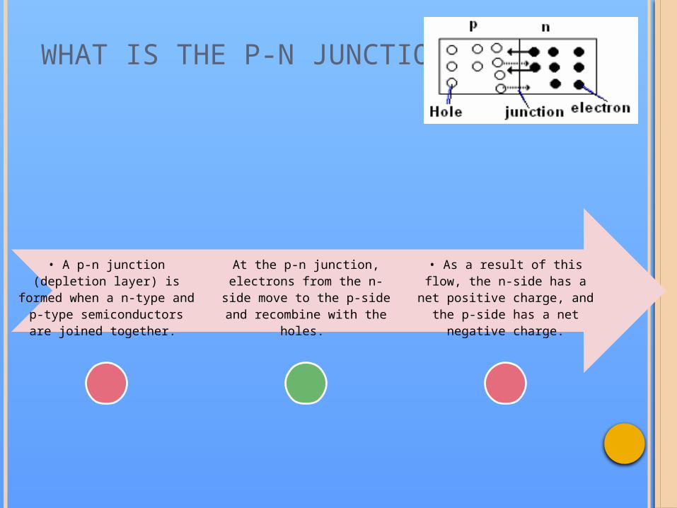
WHAT IS THE P-N JUNCTION?
• A p-n junction (depletion layer) is formed when a n-
type and p-type semiconductors are joined
together.
At the p-n junction, electrons from the n-side move to the p-side and recombine with
the holes.
• As a result of this flow, the n-side has a net positive
charge, and the p-side has a net negative charge.

WHAT IS THE DEPLETION LAYER?
The region around the
junction is left with neither
holes nor free electrons.
• This neutral region which has no charge
carriers is called the depletion
layer.
• This layer which has no
charge carrier is a poor
conductor of electricity.
Figure shows the depletion layer and junction voltage of a diode.• In order for electric current to flow through the
diode, the voltage applied across the diode must exceed the junction voltage.
• The junction voltages for germanium and silicon are approximately 0.1V and 0.6V respectively.

WHAT IS FORWARD-BIASED ? The p-type of the diode is
connected to the positive terminal and the n-type is connected to the negative terminal of a battery.
The diode conducts current because the holes from the p-type material and electrons from the n-type material are able to cross over the junction.
A light bulb will light up. The depletion layer is narrow,
and the resistance of the diode decreases.
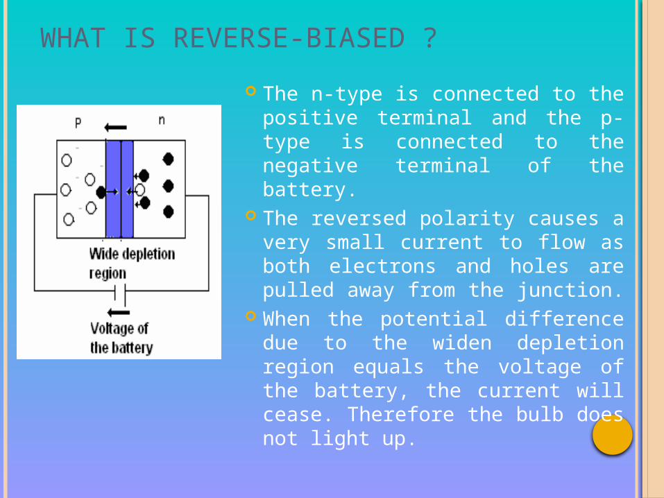
WHAT IS REVERSE-BIASED ?
The n-type is connected to the positive terminal and the p-type is connected to the negative terminal of the battery.
The reversed polarity causes a very small current to flow as both electrons and holes are pulled away from the junction.
When the potential difference due to the widen depletion region equals the voltage of the battery, the current will cease. Therefore the bulb does not light up.

When a p-n junction diode is in a forward-biased
arrangement, it only allows the current to flow from the anode to the cathode. It is
said to act as a valve.
A diode can convert alternating current into direct
current. This is known as rectification. So, a diode can
act as a rectifier.
An alternating current is a current which changes its
direction with a certain frequency. This is due to the
alternate change of the polarity of the power supply
DIODE AS A RECTIFIER

A complete cycle of alternating current consists of 2 half cycles; a positive half-cycle negative half-cycle
There are 2 ways to convert an alternating current into a direct current: Half-wave rectification Full-wave rectification

The current can only flow in the forward direction through the diode.
In the first half-cycle, the diode is forward-biased. The current can flow through the diode
In the second half-cycle, the diode is reverse-biased. The diode blocks the current.
The process of rectification using a diode which allows current to flow in the half-cycle is known as half-wave rectification
Half-wave rectification
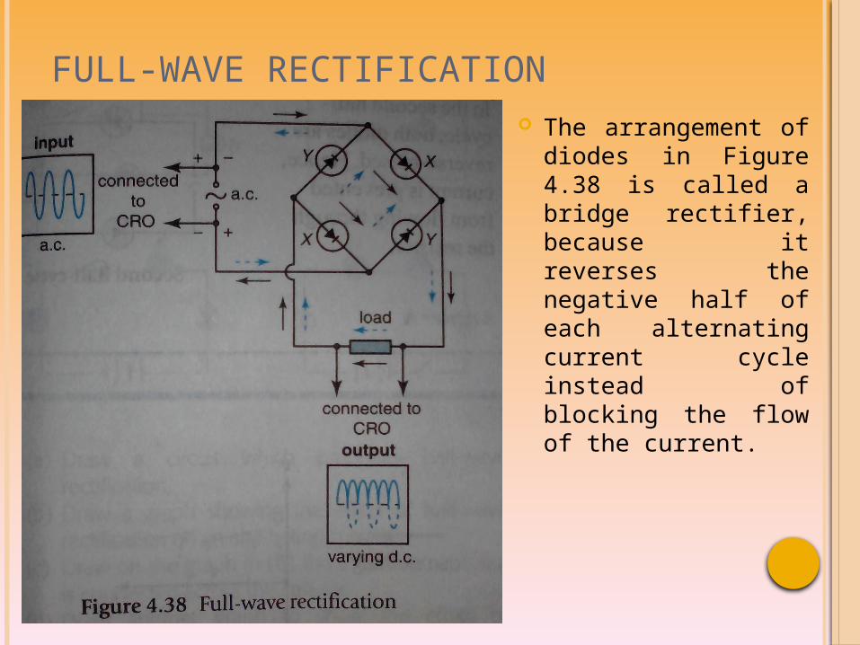
FULL-WAVE RECTIFICATION The arrangement of
diodes in Figure 4.38 is called a bridge rectifier, because it reverses the negative half of each alternating current cycle instead of blocking the flow of the current.
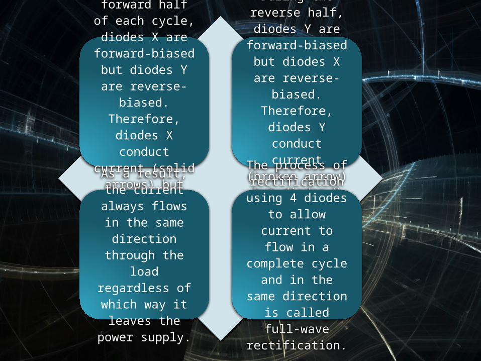
During the forward half of
each cycle, diodes X are
forward-biased but diodes Y are reverse-biased.
Therefore, diodes X conduct current (solid arrows) but
diodes Y block current.
During the reverse half, diodes Y are
forward-biased but diodes X are reverse-biased.
Therefore, diodes Y conduct current
(broken arrow) but diodes X block current.
As a result, the current always
flows in the same direction through
the load regardless of which way it
leaves the power supply.
The process of rectification using 4 diodes to allow current to flow in a complete cycle and in the same
direction is called full-wave
rectification.

The output from a rectifier circuit can be smoothed by connecting a capacitor across the load, as shown in Figure 4.39
During the forward peaks (positive half-cycles), the capacitor is charged up. Energy is stored in the capacitor.
In between the forward peaks(negative half-cycles), the capacitor releases its charge (discharges). It discharges partly through the load. The energy stored in the capacitor acts as a reservoir and maintains the potential difference across the load.
SMOOTHING

Click icon to add pictureFigure 4.40 shows
the potential difference for half-wave rectification with smoothing.A capacitor with
great capacitance produces a smoother
current. This is because the
capacitor can store more charge.


![Semiconductor Diodes [Demo]](https://static.fdocuments.in/doc/165x107/577d294d1a28ab4e1ea66956/semiconductor-diodes-demo.jpg)