Heterojunctions and Schottky Diodes on Semiconductor ...
170
University of Kentucky University of Kentucky UKnowledge UKnowledge University of Kentucky Doctoral Dissertations Graduate School 2010 Heterojunctions and Schottky Diodes on Semiconductor Heterojunctions and Schottky Diodes on Semiconductor Nanowires for Solar Cell Applications Nanowires for Solar Cell Applications Piao Liu University of Kentucky, [email protected] Right click to open a feedback form in a new tab to let us know how this document benefits you. Right click to open a feedback form in a new tab to let us know how this document benefits you. Recommended Citation Recommended Citation Liu, Piao, "Heterojunctions and Schottky Diodes on Semiconductor Nanowires for Solar Cell Applications" (2010). University of Kentucky Doctoral Dissertations. 77. https://uknowledge.uky.edu/gradschool_diss/77 This Dissertation is brought to you for free and open access by the Graduate School at UKnowledge. It has been accepted for inclusion in University of Kentucky Doctoral Dissertations by an authorized administrator of UKnowledge. For more information, please contact [email protected].
Transcript of Heterojunctions and Schottky Diodes on Semiconductor ...
University of Kentucky University of Kentucky
UKnowledge UKnowledge
University of Kentucky Doctoral Dissertations Graduate School
2010
Heterojunctions and Schottky Diodes on Semiconductor Heterojunctions and Schottky Diodes on Semiconductor
Nanowires for Solar Cell Applications Nanowires for Solar Cell Applications
Piao Liu University of Kentucky, [email protected]
Right click to open a feedback form in a new tab to let us know how this document benefits you. Right click to open a feedback form in a new tab to let us know how this document benefits you.
Recommended Citation Recommended Citation Liu, Piao, "Heterojunctions and Schottky Diodes on Semiconductor Nanowires for Solar Cell Applications" (2010). University of Kentucky Doctoral Dissertations. 77. https://uknowledge.uky.edu/gradschool_diss/77
This Dissertation is brought to you for free and open access by the Graduate School at UKnowledge. It has been accepted for inclusion in University of Kentucky Doctoral Dissertations by an authorized administrator of UKnowledge. For more information, please contact [email protected].

ABSTRACT OF DISSERTATION
Piao Liu
The Graduate School
University of Kentucky
2010
Heterojunctions and Schottky Diodes on Semiconductor Nanowires for Solar Cell
Applications
ABSTRACT OF DISSERTATION
A dissertation submitted in partial fulfillment of the requirements for the degree of
Doctor of Philosophy in the College of Engineering at the University of Kentucky
By
Piao Liu
Research Advisor: Dr. Vijay P. Singh, Professor of Electrical and Computer
Engineering
Lexington, Kentucky
2010
Copyright © Piao Liu 2010
ABSTRACT OF DISSERTATION
Heterojunctions and Schottky Diodes on Semiconductor Nanowires for Solar Cell
Application
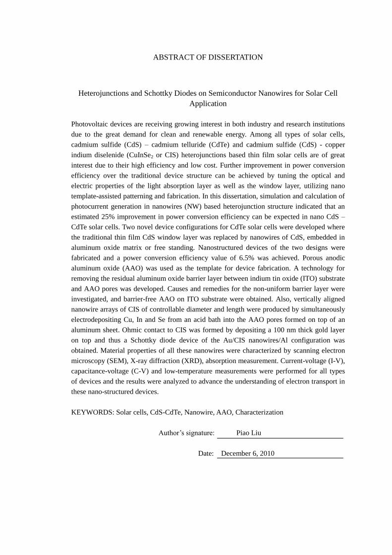
Photovoltaic devices are receiving growing interest in both industry and research institutions
due to the great demand for clean and renewable energy. Among all types of solar cells,
cadmium sulfide (CdS) – cadmium telluride (CdTe) and cadmium sulfide (CdS) - copper
indium diselenide (CuInSe2 or CIS) heterojunctions based thin film solar cells are of great
interest due to their high efficiency and low cost. Further improvement in power conversion
efficiency over the traditional device structure can be achieved by tuning the optical and
electric properties of the light absorption layer as well as the window layer, utilizing nano
template-assisted patterning and fabrication. In this dissertation, simulation and calculation of
photocurrent generation in nanowires (NW) based heterojunction structure indicated that an
estimated 25% improvement in power conversion efficiency can be expected in nano CdS –
CdTe solar cells. Two novel device configurations for CdTe solar cells were developed where
the traditional thin film CdS window layer was replaced by nanowires of CdS, embedded in
aluminum oxide matrix or free standing. Nanostructured devices of the two designs were
fabricated and a power conversion efficiency value of 6.5% was achieved. Porous anodic
aluminum oxide (AAO) was used as the template for device fabrication. A technology for
removing the residual aluminum oxide barrier layer between indium tin oxide (ITO) substrate
and AAO pores was developed. Causes and remedies for the non-uniform barrier layer were
investigated, and barrier-free AAO on ITO substrate were obtained. Also, vertically aligned
nanowire arrays of CIS of controllable diameter and length were produced by simultaneously
electrodepositing Cu, In and Se from an acid bath into the AAO pores formed on top of an
aluminum sheet. Ohmic contact to CIS was formed by depositing a 100 nm thick gold layer
on top and thus a Schottky diode device of the Au/CIS nanowires/Al configuration was
obtained. Material properties of all these nanowires were characterized by scanning electron
microscopy (SEM), X-ray diffraction (XRD), absorption measurement. Current-voltage (I-V),
capacitance-voltage (C-V) and low-temperature measurements were performed for all types
of devices and the results were analyzed to advance the understanding of electron transport in
these nano-structured devices.
KEYWORDS: Solar cells, CdS-CdTe, Nanowire, AAO, Characterization
Author‟s signature: Piao Liu
Date: December 6, 2010

Heterojunctions and Schottky Diodes on Semiconductor Nanowires for Solar Cell
Applications
By
Piao Liu
Dr. Vijay Singh
Director of Dissertation
Dr. Stephen Gedney
Director of Graduate Studies
December 6, 2010
Date
RULES FOR THE USE OF DISSERTATION
Unpublished dissertations submitted for the Doctor‟s degree and deposited in the
University of Kentucky Library are a rule open for inspection, but are to be used only
with due regard to the rights of the authors. Bibliographical references may be noted,
but quotations or summaries of parts may be published only with the permission of
the author, and with the usual scholarly acknowledgements.
Extensive copying or publication of the theses in whole or in part also requires the
consent of the Dean of the Graduate School of the University of Kentucky.
A library that borrows this dissertation for use by its patrons is expected to secure the
signature of each user.
DISSERTATION
Piao Liu
The Graduate School
University of Kentucky
2010
Heterojunctions and Schottky Diodes on Semiconductor Nanowires for Solar Cell
Applications
DISSERTATION
A dissertation submitted in partial fulfillment of the requirements for the degree of
Doctor of Philosophy in the College of Engineering at the University of Kentucky
By
Piao Liu
Research Advisor: Dr. Vijay P. Singh, Professor of Electrical and Computer
Engineering
Lexington, Kentucky
2010
Copyright © Piao Liu 2010

To my wife Yanling, for her encouragement and support.
iii
ACKNOWLEDGMENTS
I would like to express my deepest gratitude to my advisor, Dr. Vijay P. Singh, who
first introduced me to the fields of solar cell and nanotechnology. He gave me the best
opportunity to work on this interesting and challenging research topic. Special thanks
also goes to Drs. Zhi Chen, Todd Hastings, J. Zach Hilt, and Fuqian Yang, who served
as my Ph.D. dissertation committee. I extend my thanks as well to the numerous
professors whose classes I attended in the doctoral program at the University of
Kentucky. Finally I would like to honor my parents who greatly supported me to
pursue my graduate studies in the United States.
iv
Table of Contents
Acknowledgements……………………………………………………...…….….…..iii
Table of Contents…………………………………………….…………...……..……iv
List of Tables………………………………………………...……………………….vii
List of Figures………………………………………………...……………………..viii
1. Introduction………………………………..………………………..……….…….1
1.1 Growing demand for electricity….…………………….……………….………..1
1.2 The technology of photovoltaic cells can deliver a large portion of U.S. needs ...5
1.3 Generation and storage of electricity produced by solar cell arrays……………..7
2. Theory ……………………………..……………………….……….…………….10
2.1 General concepts and theories on solar cells ………….………………………..10
2.2 Different types of solar cells ………………………………………..………….16
2.2.1 Silicon solar cells………………………………..……………….………….16
2.2.2 CdS based inorganic heterojunction solar cells…...........................................18
2.2.3 Organic solar cells…………………………………………………….……..26
2.2.4 Other types of solar cells………………………………..…………….……..30
3. Advantages of Nano-structured Solar Cells ……………………….…...………33
3.1 Definition of nanotechnology ………………………………….…....…………33
3.2 Application of nanotechnology in solar cell development …………….………33
3.3 Simulation of efficiency enhancement in nano CdS-CdTe solar cells ......……..36
4. Barrier-free AAO Templates on ITO Substrates ………………..…..…………46
4.1 The wide use of AAO in template-assisted device fabrication …….…………..46
v
4.2 Description of experimental details ….…………………………………………48
4.3 Barrier layer study of AAO templates on ITO substrates ……….……….…….51
4.3.1 The mechanism of non-uniform barrier layer formation ……………..…….51
4.3.2 Study of anodization process …………….....................................................54
4.3.3 The effect of titanium layer in anodization ……….………………….……..59
4.3.4 The effect of non-uniform barrier layer in nanowire electrodeposition ….....62
4.3.5 Barrier-free AAO template and uniform nanowire electrodeposition ..……..64
4.4 Comments ………………….………….…………………………..……………70
5. Nanostructured CdS – CdTe Solar Cells ………..………………...……………73
5.1 New design of CdS – CdTe solar cell by nano engineering ……………………73
5.2 Fabrication process of CdS NW – CdTe solar cell …...……….………………..78
5.2.1 Fabrication of ordered AAO template on i-SnO2/ITO/Glass substrate ….....78
5.2.2 Fabrication and characterization of CdS NW ................................................81
5.2.3 Deposition of CdTe layer and making contact ……………………….……..87
5.3 Characterization of CdS NW – CdTe solar cell ……………………..…………90
5.3.1 Current-Voltage (I-V) measurement under illumination ……….……….…..90
5.3.2 I-V characteristic of the champion planar cell ...............................................91
5.3.3 Analysis of the champion planar cell …….……….………………….……..92
5.3.4 Comparison of the champion nano & planar cell …………………….….....95
5.3.5 Effects of CdS NW length on the device performance …………….……...100
5.3.6 Capacitance-Voltage (C-V) measurement of CdS NW – CdTe solar cell ....103
5.3.7 Low-temperature I-V measurement of CdS NW – CdTe solar cell .......…..107
5.4 Comments …………………………….………………………….……………112
6. CuInSe2 Nanowires – Al Schottky Diode …………………………...…………113
6.1 Why is CIS nanowire interesting? ……………………………..……...………113
6.2 Fabrication procedure of CIS NW – Al Schottky diode ..…………..…………114
6.3 Characterization and analysis of CIS NW – Al Schottky diode ..…….….……117
6.3.1 CIS nanowire characteristics …………………….…….…………..………117

vi
6.3.2 CIS NW – Al Schottky diode I-V characteristics .........................................119
6.3.3 CIS NW – Al Schottky diode C-V characteristics ……….…………..……122
6.3.4 Band diagram of CIS NW – Al Schottky diode …………………………...126
6.4 Comments …………………………….……………………………….………128
7. Conclusion and Suggestions for Future Work …….……………..………..….130
Appendix A Program code …………….…….…………….…….……..…….……133
Reference……………………………………………………….………..…………141
Vita …….……………………………………………………….………………..…152
vii
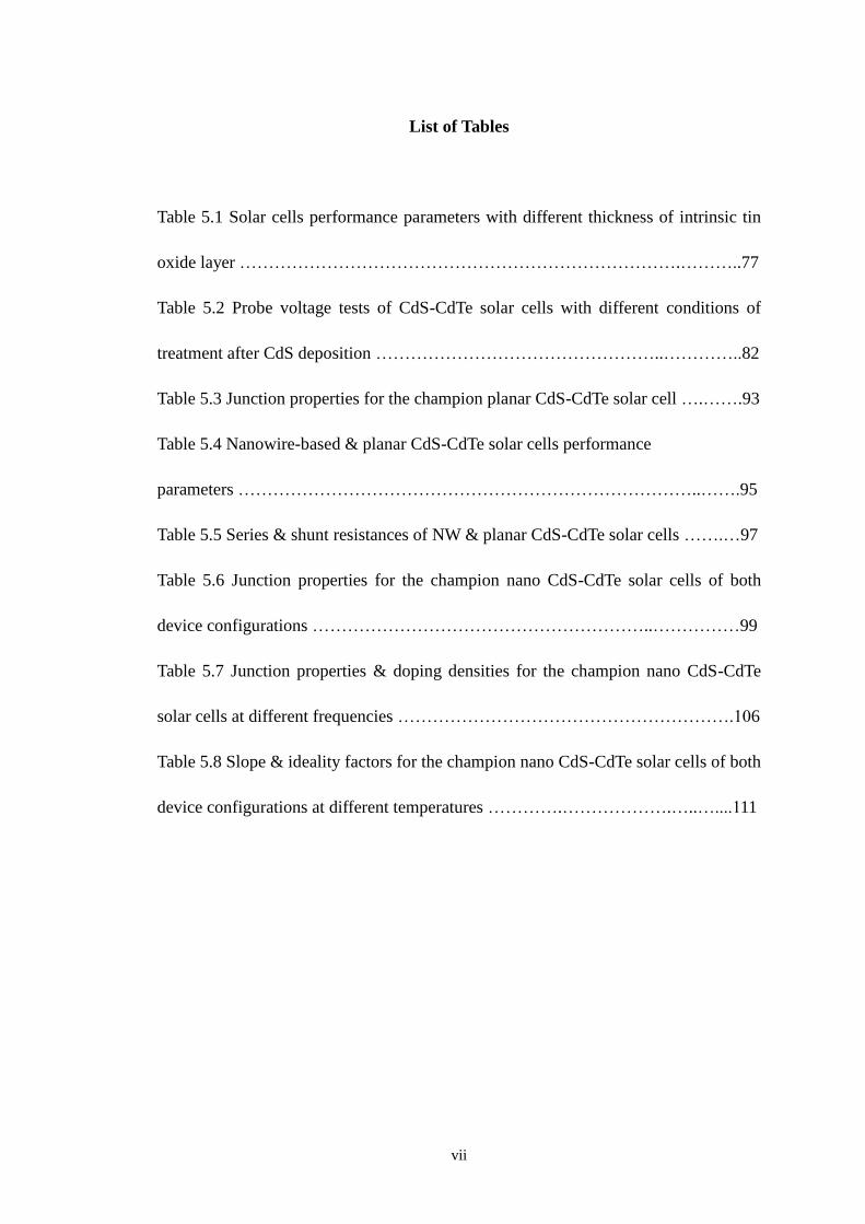
List of Tables
Table 5.1 Solar cells performance parameters with different thickness of intrinsic tin
oxide layer ………………………………………………………………….………..77
Table 5.2 Probe voltage tests of CdS-CdTe solar cells with different conditions of
treatment after CdS deposition …………………………………………..…………..82
Table 5.3 Junction properties for the champion planar CdS-CdTe solar cell ….…….93
Table 5.4 Nanowire-based & planar CdS-CdTe solar cells performance
parameters ……………………………………………………………………..…….95
Table 5.5 Series & shunt resistances of NW & planar CdS-CdTe solar cells …….…97
Table 5.6 Junction properties for the champion nano CdS-CdTe solar cells of both
device configurations …………………………………………………..……………99
Table 5.7 Junction properties & doping densities for the champion nano CdS-CdTe
solar cells at different frequencies ………………………………………………….106
Table 5.8 Slope & ideality factors for the champion nano CdS-CdTe solar cells of both
device configurations at different temperatures ………….……………….…..…....111
viii
List of Figures
Fig 1.1 World consumption of electricity by energy source ……….…….…………...2
Fig 1.2 2008 United States consumption of electricity by energy source …….….…...3
Fig 1.3 Electricity consumption in GkWh ……………...…………………….……....4
Fig 1.4 Diagram of a photovoltaic generation plant …….………………….….……..8
Fig 1.5 Diagram of a solar cell system for a home or business ……….………...……9
Fig 2.1 Basic operation of a solar cell ……….………………………..……………..10
Fig. 2.2 Simplest model of silicon p-n junction solar cell and I-V curve ..…...……..12
Fig. 2.3 Maximum power output of solar cells ……………………….…......……....14
Fig. 2.4 Typical heterojunction band diagram in equilibrium ………...……….…….19
Fig. 2.5 Structure of CdS-CdTe solar cells on glass substrate ..…………….……….20
Fig. 2.6 Work functions of metal and p-type semiconductor ……………….……….22
Fig. 2.7 Configuration of CuPc-based solar cell with Al electrode ………….……...29
Fig. 2.8 Energy band diagram of CuPc-based solar cell with Al electrode …………30
Fig. 3.1 Simulation of photocurrent enhancement due to absorption edge shift in CdS
NW ..………………………………………………………………….………..…….41
Fig. 3.2 Simulation of photocurrent generated in CdTe at the absence of CdS layer .42
Fig. 4.1: A typical SEM image of AAO template on ITO substrate showing
non-uniform barrier layer thickness …..……….……………………..………..…….51
Fig. 4.2: (a) A sketch of typical current versus time plot with five stages marked (b)
Example of an actual I-t curve used for monitoring the anodization process of a
Al(200nm)/Ti(5nm)/ITO/Glass sample ……………………………………….…..…55
Fig. 4.3: Cross-section view of a 30 nm Ti, 200 nm Al sample after one-hour
anodization …………………………………………………………………………..58
Fig. 4.4: CdS electrodeposited into non-uniformly opened templates, resulting in
ix
non-uniform nanowires and low filling ratio (top view) ………………………….....64
Fig. 4.5: Cross-section image of a barrier-free template with thickness of 200
nm …………………….………………………………..………….…………………65
Fig. 4.6: Cross-section image of CdS nanowires grown through the barrier-free AAO
template ………………………………………………………………………..…….66
Fig. 4.7: Cross-section image of a barrier-free template with AAO thickness of 1
micron fabricated on glass/ITO substrate ……………..……………………………..67
Fig. 4.8: Uniform deposition of CdS nanowires into a barrier-free template. The
template was dissolved in NaOH for SEM imaging (top view) ……….…………….68
Fig. 4.9: Transmittance of AAO template on ITO versus pure ITO substrate .............69
Fig. 4.10: J-V curve of CdS/gold Schottky diode on CdS nanowires embedded in (a)
non-uniform and (b) uniform AAO templates …………………………………..…...70
Fig. 5.1: Flow chart of the newly designed fabrication process of CdS nanowires
based CdTe-CdS solar cells …………………………………...………………….….75
Fig. 5.2: (a) Surface morphology of sputtered SnO2 layer. (b) Surface morphology of
evaporated and annealed SnO2 layer ………….…………….………..………..…….79
Fig. 5.3: Distorted AAO templates on top of thermal evaporated and annealed SnO2
layer …………………………………………………………...……………………..80
Fig. 5.4: Ordered porous alumina templates on top of sputtered SnO2 layer on
ITO/Glass for building front-wall structured nanowire CdS/CdTe based solar
cells …………………………………………………………………………………..80
Fig. 5.5: 400 nm AAO template on 250 nm i-SnO2 layer on ITO/Glass ....….......…..81
Fig. 5.6: SEM image of free-standing CdS nanowire arrays (top view). (a) ~200 nm in
length (aspect ratio < 5). (b) ~400 nm in length (aspect ratio > 5) ………………….84
Fig. 5.7: (a) TEM image of released CdS nanowires. (b) SEM image of free-standing
CdS nanowires on i-SnO2/ITO/Glass substrate (cross-section view) ..…….………..85
Fig. 5.8: HR-TEM image of a single CdS nanowire, showing uniform atom
arrangement ………………………………………………………………………….86
Fig. 5.9: XRD pattern of free-standing CdS nanowires on ITO substrate ......……....87
x
Fig. 5.10: After the removal of AAO templates, the Cadmium telluride layer was
evaporated on top of the CdS. CdTe did not fill the gaps between the CdS
nanowires …………………………………………………...………...……….…….88
Fig. 5.11: Champion solar cell I-V characteristics of (a) Design A: CdTe on CdS
nanowires embedded in AAO; (b) Design B: CdTe on free-standing CdS
nanowires ……………..………………………………….….……………………....90
Fig. 5.12: Champion planar CdS-CdTe solar cell I-V characteristic ………..……….92
Fig. 5.13: Semi-log plots for the champion planar CdS-CdTe solar cell (a) ln (J) vs. V
in dark (b) ln (J + JL) vs. V under illumination …………………...………….……...94
Fig. 5.14: Residues and junks in-between and on top of the free-standing CdS
NWs ………………………………………………………………….………………98
Fig. 5.15: Top: open-circuit voltage and short-circuit current density of solar cell (a)
Design A (b) Design B; Bottom: fill factor and efficiency of (c) Design A (d) Design
B ……………………..……..…………………….……..…...………..……………101
Fig. 5.16: Capacitance vs. applied voltage for the champion nano CdS-CdTe solar cell
at (a) 5 KHz (b) 30 KHz (c) 300 KHz……….………………………..………..…..105
Fig. 5.17: 1/C2-V plot of the champion nano CdS-CdTe solar cell at 30 KHz ….....105
Fig. 5.18: Dark I-V measurement of the champion CdS NW - CdTe solar cells of (a)
Design A (b) Design B at different temperatures .…………………….…......……..109
Fig. 5.19: α vs. 1000/T plots of the champion CdS NW - CdTe solar cells of (a)
Design A (b) Design B ……………………………………………..………………110
Fig. 6.1: Configuration of the device for CIS nanowire - Al Schottky diode
measurement …………………………………………….………………………….115
Fig. 6.2: SEM images of the CIS nanowires inside porous alumina template: (a) top
view (b) cross-section view …………………………….….…..………..…….……118
Fig. 6.3: A typical J-V curve of Al/CIS nanowire Schottky diode …….…….……..120
Fig. 6.4: 1/C2-V curve of Al/CIS nanowire Schottky diode measured at 1MHz .….123
Fig. 6.5: Sketch of the energy band diagram of a CIS-Al Schottky diode …..……..127

1
1. Introduction
1.1 Growing demand for electricity
Energy consumption of the whole world is increasing exponentially for these decades,
but the supply of fossil fuels does not have an exponential growth as the demand does.
An emerging technology - photovoltaic (PV) cells, could deliver a large portion of
United States‟ needs in the next 40 years if they are properly developed. The
importance of developing renewable energy sources is a topic that has been discussed
for decades. However, the choice of energy source is largely dependent on its
availability. According to the EIA[1]
, the United States and China have vast coal
reserves, while Iceland gets virtually all of its electricity from either hydroelectric or
geothermal power plants and 98.5 percent of Norway‟s electricity is generated from
hydropower[2]
. France, because of its shortage of fossil fuels and limited suitable
hydroelectric sites, depends on nuclear power for almost 80 percent of its electricity.
Due to the polluting nature of coal, both China and the United States are in the process
of expanding their nuclear power capabilities substantially within the next decade.
Denmark gets much of its electrical power from wind turbines and Germany, which
also has limited fossil fuel resources, is currently investing heavily in its solar power
capability.
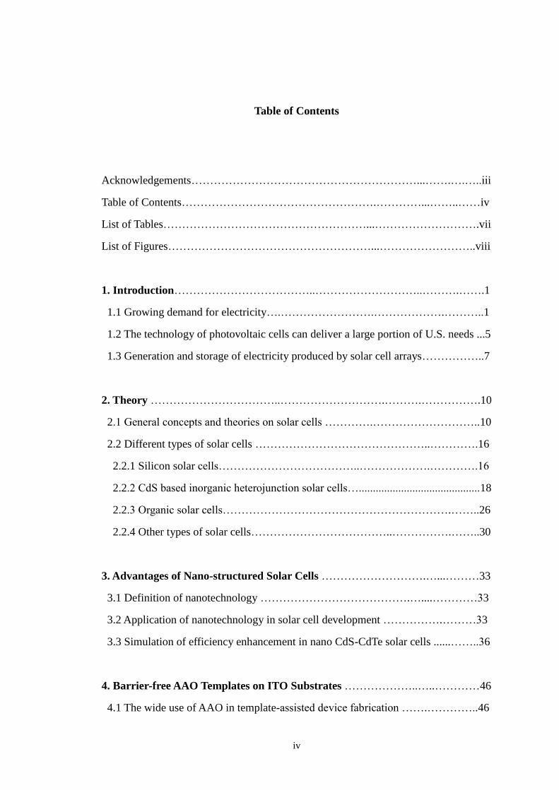
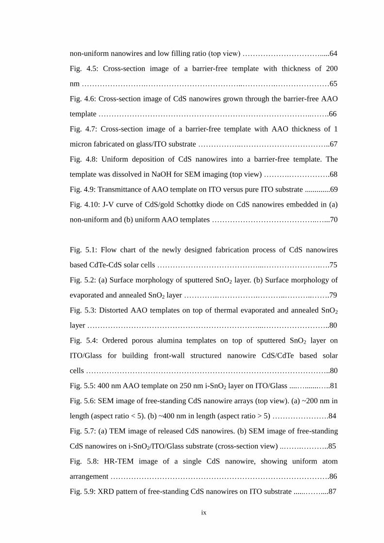
Figure 1.1 gives the percentages of various sources used to generate the world‟s
electrical energy in 2007[1]
. Also, given in parentheses are the amounts of electricity
2
generated by these sources in giga-kilowatt-hours (GkWh). The worldwide total
amount of consumed electricity in 2007 was 16,990 GkWh, which is the energy
equivalent of a little over ten billion barrels of oil or 2.57 billion tons of coal. It is seen
from figure 1.1 that fossil fuels are used to generate about two-thirds of the world‟s
electricity[2]
.
Figure 1.1: World consumption of electricity by energy source.
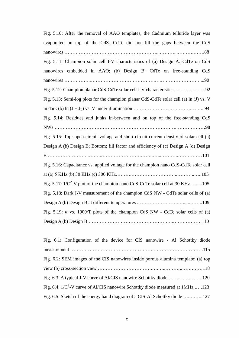
The 2008 amounts and percentages of the sources used to generate electricity within the
United States are given in figure 1.2[1]
. As in the United States, about half of the world‟s
electricity is generated by coal. Neither the amounts in figure 1.1 nor 1.2 includes the
generation and distribution losses.
3
Figure 1.2: 2008 United States consumption of electricity by energy source.
Figure 1.3 shows the electricity consumption, excluding generation and distribution
losses, in both the world and United States during the period 1980 through 2007[1]
.
Superimposed on the actual data curves are the exponential approximation of the world
data and the linear approximation of the United States data. The exponential
approximation of the world data shows a compounded three percent increase per
year[2]
. By including the necessary excess capacity, this growth implies that in the
succeeding years the worldwide generating capacity would need to be increased by
122.9 GW, 126.3 GW, 130.1 GW and so on just to keep pace with demand. If the recent
trend continues, by 2040 the worldwide demand would be 43,230 GkWh, more than
two and a half times its 2007 demand. The United State has increased consumption at a
linear rate of 74.68 GkWh per year and would need to add 18.7 GW to its generating
capacity each year to meet its future demands. Its demand in 2040 would be 6490
GkWh. To add 18.7 GW of capacity would require the construction of over eighteen
1,000 MW generating plants[2]
.
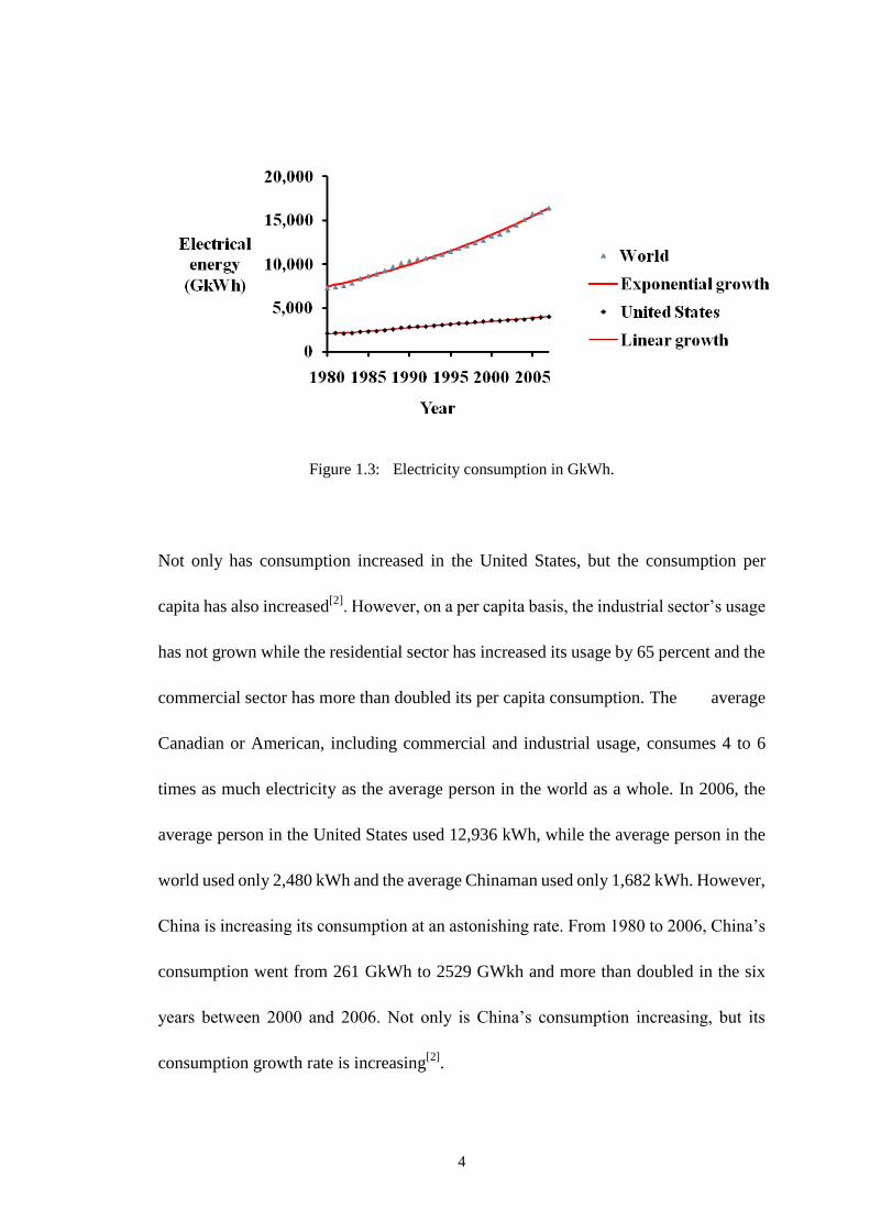
4
Figure 1.3: Electricity consumption in GkWh.
Not only has consumption increased in the United States, but the consumption per
capita has also increased[2]
. However, on a per capita basis, the industrial sector‟s usage
has not grown while the residential sector has increased its usage by 65 percent and the
commercial sector has more than doubled its per capita consumption. The average
Canadian or American, including commercial and industrial usage, consumes 4 to 6
times as much electricity as the average person in the world as a whole. In 2006, the
average person in the United States used 12,936 kWh, while the average person in the
world used only 2,480 kWh and the average Chinaman used only 1,682 kWh. However,
China is increasing its consumption at an astonishing rate. From 1980 to 2006, China‟s
consumption went from 261 GkWh to 2529 GWkh and more than doubled in the six
years between 2000 and 2006. Not only is China‟s consumption increasing, but its
consumption growth rate is increasing[2]
.

5
Although oil and gas fields and coal mines are still being discovered by exploration
companies, the supply of fossil fuels does not have an exponential growth as the
demand of energy does. Likewise as the non-renewable energy sources scarce the price
of generating electricity from them increases, this underdevelopment of fossil fuels
supply added to the exponential growth of the demand could bring important economic
and political problems[2]
.
1.2 The technology of photovoltaic cells can deliver a large portion of U.S. needs
A big part of the renewable energy sources available in the world is the energy
delivered by the sun. There is a wide variety of useful devices involving the interaction
of photons and electronics. Solar cell/module is one of the most commonly used
electroluminescence devices. Nowadays, solar cells have been widely used for many
different applications. Solar cells are dominant in the region of long-duration power
supply for satellites and space vehicles. Solar cells have also achieved great success in
small-scale terrestrial applications. Compared with conventional energy resources such
as gasoline, solar cells show great advantages in terms of no pollution and unlimited
source. Recently, research and development of variety of materials used for solar cells
and fabrication process or special technology to produce high efficient solar cells have
increased. In the near future, the costs of fabrication process will be economically
feasible and wide use of solar energy will become realistic. This generating technology
could deliver a large portion of United States‟ needs in the next 40 years[3]
.
6
The southwestern desert of the United States has a generation capacity of 2940GW.
This generation capacity could be obtained converting this energy from the sun into
electrical power by installing photovoltaic plants.
The development of this new generating plants means that the power grid also has to be
updated. The United States will have to build a direct current (DC), high-voltage
transmission line infrastructure to transmit electricity from Southwestern U.S. to cities
and regions across the nation.
The energy generated by PV plants will have to be stored in order to be able to use it
during the night when there is no electricity generated by this type of plants. This can be
made using the electrical energy at the destination region to produce compressed air,
which can be stored in underground caverns and other storage facilities used at present
for storing natural gas. At nighttime the compressed air will be released in demand, to
turn turbines that generate electricity for regional needs, aided by burning small
amounts of natural gas[2]
.
This electrical development model states that by 2050 solar power could be able to
provide 69% of the electrical energy and 35% of the total energy needs of United
States. This will end the dependence on foreign oil of the United States and will reduce
significantly the greenhouse gas emissions. Also, a change of technology and update of
the power grid will increase the number of domestic jobs.
7
The solar power development could even decrease the energy demand. Assuming the
United States had a 1% annual electric energy demand growth, by 2050, the total
energy consumption will actually become lower than today. In 2006 100 quadrillion
Btu were consumed. This will fall to 93 quadrillion Btu by 2050 because, today, a lot of
energy is consumed just to extract and process fossil fuels and later, even more energy
is wasted in burning the fuels and controlling their emissions[2]
.
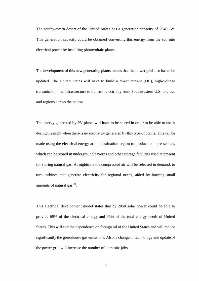
1.3 Generation and storage of electricity produced by solar cell arrays
A photovoltaic cell generation plant consists of several panels containing large
photovoltaic sheets or arrays of solar cells and connecting them together in such a way
that they produce a suitable voltage and current. This energy has to be stored in the day
so it can also be used in the night. A very popular medium used to store electrical
energy generated by small photovoltaic arrays is a battery array. However the battery
technology is not able to store large quantities and their life time is not high enough to
be an affordable solution for a photovoltaic generation plant. A proposed method to
store the energy generated by the PV plant is the use of air compressors and
underground gas storage facilities. Figure 1.4 shows a diagram of a generic
photovoltaic generation plant (arrays of solar cells/modules connected in series or
parallel) and storage facilities[2]
.
8
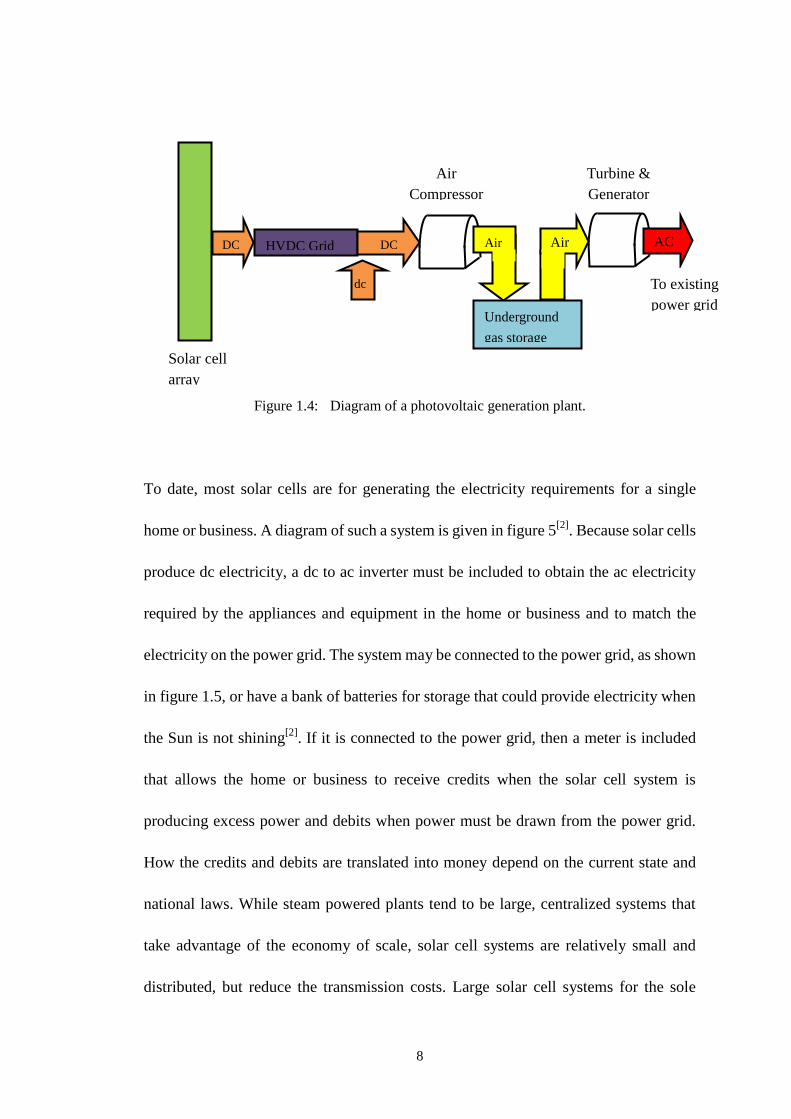
Figure 1.4: Diagram of a photovoltaic generation plant.
To date, most solar cells are for generating the electricity requirements for a single
home or business. A diagram of such a system is given in figure 5[2]
. Because solar cells
produce dc electricity, a dc to ac inverter must be included to obtain the ac electricity
required by the appliances and equipment in the home or business and to match the
electricity on the power grid. The system may be connected to the power grid, as shown
in figure 1.5, or have a bank of batteries for storage that could provide electricity when
the Sun is not shining[2]
. If it is connected to the power grid, then a meter is included
that allows the home or business to receive credits when the solar cell system is
producing excess power and debits when power must be drawn from the power grid.
How the credits and debits are translated into money depend on the current state and
national laws. While steam powered plants tend to be large, centralized systems that
take advantage of the economy of scale, solar cell systems are relatively small and
distributed, but reduce the transmission costs. Large solar cell systems for the sole
Turbine &
Generator
Air
Compressor
HVDC Grid DC
dc
Solar cell
array
DC Air
Underground
gas storage
Air AC
To existing
power grid

9
purpose of supplying power to the grid will become common when they become
economically competitive[2]
.
Figure 1.5: Diagram of a solar cell system for a home or business.
dc
dc
ac
ac
Meter (optional)
Inverter
Solar cell array Batteries (optional)
To/from power grid
Refrigerator
Lights
Air conditioning
Electronics
ac
10
2. Theory
2.1 General concepts and theories on solar cells
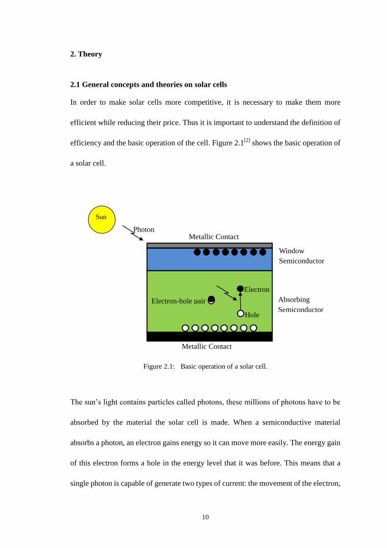
In order to make solar cells more competitive, it is necessary to make them more
efficient while reducing their price. Thus it is important to understand the definition of
efficiency and the basic operation of the cell. Figure 2.1[2]
shows the basic operation of
a solar cell.
Figure 2.1: Basic operation of a solar cell.
The sun‟s light contains particles called photons, these millions of photons have to be
absorbed by the material the solar cell is made. When a semiconductive material
absorbs a photon, an electron gains energy so it can move more easily. The energy gain
of this electron forms a hole in the energy level that it was before. This means that a
single photon is capable of generate two types of current: the movement of the electron,
Metallic Contact
Metallic Contact
Absorbing
Semiconductor
Sun
Electron-hole pair
Electron
Hole
Photon
Window
Semiconductor
11
and the filling of the hole. For the case of this explanation we could consider the
electron and the hole as two particles with the same amount of energy but different sign.
The movement of these electrons and holes is what creates current. In order to collect
these electrons and holes a different type of semiconductor is used called window. This
semiconductor has two functions: allow the transit of the photon and generate an
electric field capable of separate the electron from the hole. In this way a metal
connected to the window can collect the electrons and a metal connected to the absorber
can collect the holes. This is how the energy from the sun is converted. The efficiency
of a given solar cell will depend in how transparent is the window semiconductor, how
absorbing is the absorber semiconductor and how many electrons and holes are
collected[2]
.
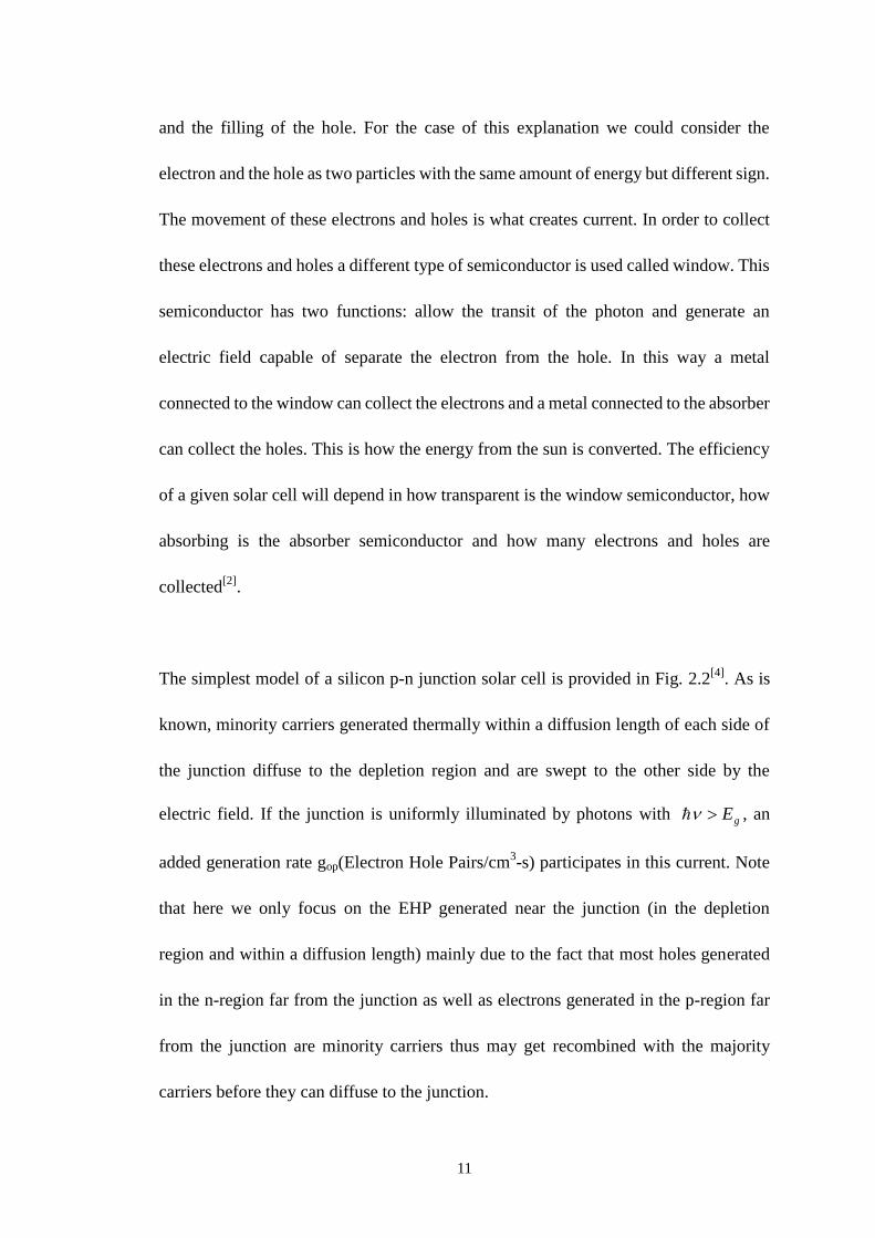
The simplest model of a silicon p-n junction solar cell is provided in Fig. 2.2[4]
. As is
known, minority carriers generated thermally within a diffusion length of each side of
the junction diffuse to the depletion region and are swept to the other side by the
electric field. If the junction is uniformly illuminated by photons with gE , an
added generation rate gop(Electron Hole Pairs/cm3-s) participates in this current. Note
that here we only focus on the EHP generated near the junction (in the depletion
region and within a diffusion length) mainly due to the fact that most holes generated
in the n-region far from the junction as well as electrons generated in the p-region far
from the junction are minority carriers thus may get recombined with the majority
carriers before they can diffuse to the junction.
12
Figure 2.2 Simplest model of silicon p-n junction solar cell and I-V curve
The resulting current due to collection of these optically generated carriers by the
junction is
WLLqAgI npopop (2.1)
If we call the reverse saturation current I0, we can add the optical generated current to
find the total reverse current with illumination. Since this current is directed from n to
p, the diode equation becomes
(2.2)
Thus the I-V curve is lowered by an amount proportional to the generation rate as we
can also see in Figure 2.2. This equation can be considered in two parts: the dark
current described by the usual diode equation and the current due to optical
generation.
13
What seems to be most attractive to us from the I-V characteristics is the fact that in
the fourth quadrant, the junction voltage is positive while the current is negative. In
this case power is delivered from the junction to the external circuit which functions
as solar cells. This is the most critical principles that how p-n junction devices can
work as a power source which convert solar energy into electrical energy.
If we consider that how much power can be delivered by an individual device, the
voltage is restricted to values less than the contact potential, which typically is less
than 1 V and the current is in the range of 10~100 mA for a junction with an area of
about 1 cm2. However, typically we will use arrays of p-n junction solar cells
depending on how much power we need to supply. Such solar cells are connected in
series to obtain a high voltage and connected in parallels to acquire a large current
flow.
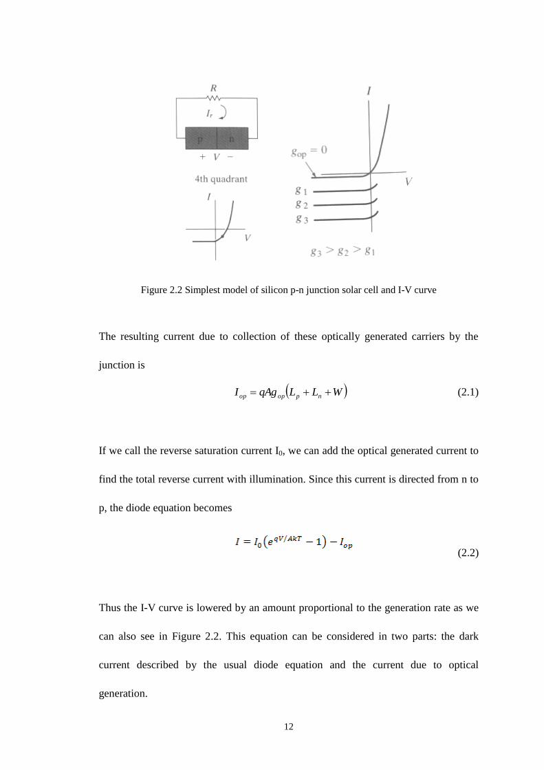
Figure 2.3[4]
shows the characteristic of solar cells with maximum power output
indicated by shaded rectangle. The open circuit voltage Voc and short circuit current
Isc are determined for a given light level by the cell properties. The maximum power
that can be delivered to a load by this solar cell occurs when the product abs(VI) is a
maximum. The ratio ImVm/IscVoc is called the fill factor, and is a merit for solar cell
design.
14
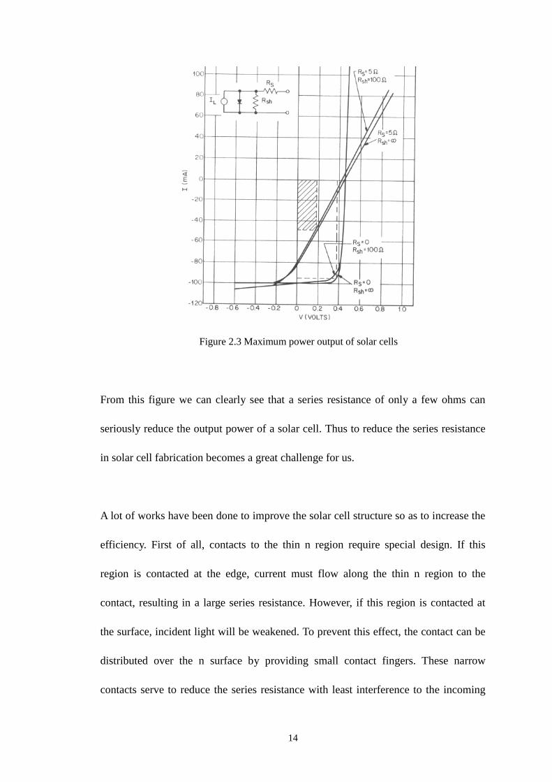
Figure 2.3 Maximum power output of solar cells
From this figure we can clearly see that a series resistance of only a few ohms can
seriously reduce the output power of a solar cell. Thus to reduce the series resistance
in solar cell fabrication becomes a great challenge for us.
A lot of works have been done to improve the solar cell structure so as to increase the
efficiency. First of all, contacts to the thin n region require special design. If this
region is contacted at the edge, current must flow along the thin n region to the
contact, resulting in a large series resistance. However, if this region is contacted at
the surface, incident light will be weakened. To prevent this effect, the contact can be
distributed over the n surface by providing small contact fingers. These narrow
contacts serve to reduce the series resistance with least interference to the incoming
15
light. To utilize a maximum amount of available optical energy, it is necessary to
design a solar cell with a large area junction. Thus the contacts are usually made grid
and the surface is usually coated with appropriate materials to reduce reflection and to
decrease surface recombination.
There are many other ways to increase the optical path of silicon solar cell to improve
absorption. Reflective back contact is one of them[4]
. Instead of a normal contact on
p-silicon side, we make the contact with reflective conducting material so that the
same optical length is achieved with only half physical thickness, which could be
closer to the minority carrier diffusion length. Other approaches, such as vertical
junction, which duplicates junctions periodically every diffusion length, pyramidal
surface, which reduces the reflective coefficient, are widely used to increase the solar
cell efficiency.
Besides, many compromises must be made in solar cell design. For example, the
junction depth must be small enough to allow minority carriers generated near the
surface to diffuse to the junction before they recombine. At the same time, the film
must be thick enough to absorb most light. What‟s more, a large contact potential is
desirable to obtain a large photovoltage since it is limited by the contact potential V0,
and therefore heavy doping is necessary according to the formula
20 lni
da
n
NN
q
kTV (2.3)

16
On the other hand, long lifetime of minority carriers is desirable and these are reduced
by doping too heavily. In practice, people use different kinds of technology for
different types of solar cells to satisfy most of these requirements. Also the cost will
be taken into consideration for large scale solar cell production.
2.2 Different types of solar cells
2.2.1 Silicon solar cells
Silicon is used to produce the most popular solar cells mainly due to the fact that we
are most familiar with it in semiconductor field. Because of the purity of silicon and
energy intensive methods, the efficiency of monocrystalline (or single crystalline)
silicon cells is relatively high and the electrical properties of individual modules are
quite stable. There is, of course, a high cost associated with the use of relatively thick
wafers of pure silicon. It accounts for roughly 40% of the entire production cost
which makes it the most significant factor. Despite the high cost, some 40% of the
solar cells produced in the world, during 2009, were single crystal silicon and,
according to the manufacturer‟s data in 2009, the highest module efficiency available
for single-crystalline silicon is 20%[5]
.
As the counter part, polycrystalline silicon solar cells can be produced using
17
lower-grade silicon material which means it allows more cost-efficient production.
Crystals of various sizes are formed during this process which means there are defects
at the edges of individual crystals. Due to the defects, the efficiency is less than that of
single-crystalline cells. The portion of polycrystalline silicon modules produced
worldwide in 2009 was just over 50% and, in general, their efficiencies were around
16 – 17 % in 2004[5]
.
However, silicon is not the best material for solar cell fabrication as far as is known.
For fully exploiting the incident light energy, we want the material bandgap to be very
small to absorb photons in red and even infrared region. While at the same time, we
want the output voltage to be as large as possible, which results in the need for wide
bandgap. A balance is achieved at the energy gap of Eg = 1.5 eV, where the product of
output voltage and current maximized. However, the bandgap of silicon is 1.1 eV
which results in a lower efficiency.
What‟s more, silicon has an indirect bandgap which leads to a much smaller
absorption coefficient (about one hundred times less than the one with a direct
bandgap). That is to say, to fully absorb incident light, we need 100 times thicker
silicon layer than other direct bandgap materials. High surface recombination rate can
be expected for a thick silicon layer, which will also result in a lower efficiency.
18
On one hand, a lot of works have been done on improving the solar cell structure to
increase the efficiency. On the other hand, researchers are looking for new materials
that could replace silicon and achieve higher efficiency, lower cost. People have
invented a lot approaches to improve the efficiency of solar cells. For example, in
many applications, heterojunction solar cells are used instead of homojunction p-n
silicon to increase the light absorption.
2.2.2 CdS based inorganic heterojunction solar cells
Heterojunctions are junctions formed between two semiconductors with different
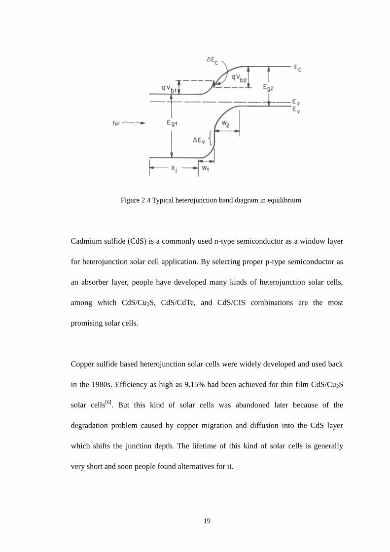
energy bandgaps. A typical heterojunction band diagram in equilibrium is shown in
Figure 2.4[4]
. Light with energy less than Eg1 but greater than Eg2 will pass through
the first semiconductor, which acts as a window, and will be absorbed by the second
semiconductor. The advantages of heterojunction solar cells over conventional p-n
junction solar cells include: a) enhanced short-wavelength spectral response because
most photons are absorbed inside the depletion region of the second semiconductor,
thus surface recombination of high-energy photons generated electron hole pairs
(EHP) greatly decreased; b) lower series resistance because the first semiconductor
can be heavily doped without causing the lifetime of minority carriers short; c) high
radiation tolerance.
19
Figure 2.4 Typical heterojunction band diagram in equilibrium
Cadmium sulfide (CdS) is a commonly used n-type semiconductor as a window layer
for heterojunction solar cell application. By selecting proper p-type semiconductor as
an absorber layer, people have developed many kinds of heterojunction solar cells,
among which CdS/Cu2S, CdS/CdTe, and CdS/CIS combinations are the most
promising solar cells.
Copper sulfide based heterojunction solar cells were widely developed and used back
in the 1980s. Efficiency as high as 9.15% had been achieved for thin film CdS/Cu2S
solar cells[6]
. But this kind of solar cells was abandoned later because of the
degradation problem caused by copper migration and diffusion into the CdS layer
which shifts the junction depth. The lifetime of this kind of solar cells is generally
very short and soon people found alternatives for it.

20
Cadmium telluride was found to be a very suitable absorbing layer for solar cells.
CdS/CdTe based solar cells have reached an efficiency of 16.5%[7]
which is close to
the predicted efficiency limit of 17.5%[8]
. This kind of solar cells has been used for a
long time and still being widely used nowadays.
Solar cells made of CdS/CdTe heterojunction are widely used as thin film solar cells
due to the near ideal bandgap properties of CdTe absorber layer. CdTe has a direct
bandgap of 1.5 eV, which is close to the perfect bandgap 1.45 eV for solar cell
application according to the theories[9]
. CdS is grown on CdTe for lattice match, and
also performs as a window layer for lights to come in and be absorbed near the
junction.
There are generally two types of substrate for growing CdS-CdTe solar cell. One is
glass or ITO coated glass, and the other one is the flexible metal foil, such as
molybdenum. The structure of glass-based CdS-CdTe solar cell is sketched in Figure
2.5[10]
.
Figure 2.5 Structure of CdS-CdTe solar cells on glass substrate

21
CdTe has a much better bandgap than silicon. However, general CdTe-CdS solar cells
are not much more efficient than silicon solar cells as we might expect. This is due to
a lot of design issues associated with the fabrication procedure of CdTe-CdS solar
cells.
First of all, it is hard to make good contact to p-CdTe layer. In many cases we wish to
have an ohmic metal-semiconductor contact which has a linear I-V characteristic in
both bias directions because we want the contact to be with minimal resistance and no
tendency to rectify signals. Ideal metal-semiconductor contacts are ohmic when the
charge induced in the semiconductor in aligning the Fermi levels is provided by
majority carriers. That is to say, there is no depletion region occurring in the
semiconductor in this case since the electrostatic potential difference required to align
the Fermi levels at equilibrium calls for accumulation of majority carriers in the
semiconductor. For example, in the case of p type CdTe layer being connected to
metal, charge induced in the p-CdTe is positive which are carried by holes. This
lowers the semiconductor electron energies relative to the metal at equilibrium. Thus
the barrier to holes flow across the junction is small and easily overcome. To achieve
ohmic contact, the work function of the metal must be larger than that of the
semiconductor ( sm ) as we can see in Figure 2.6[4]
.
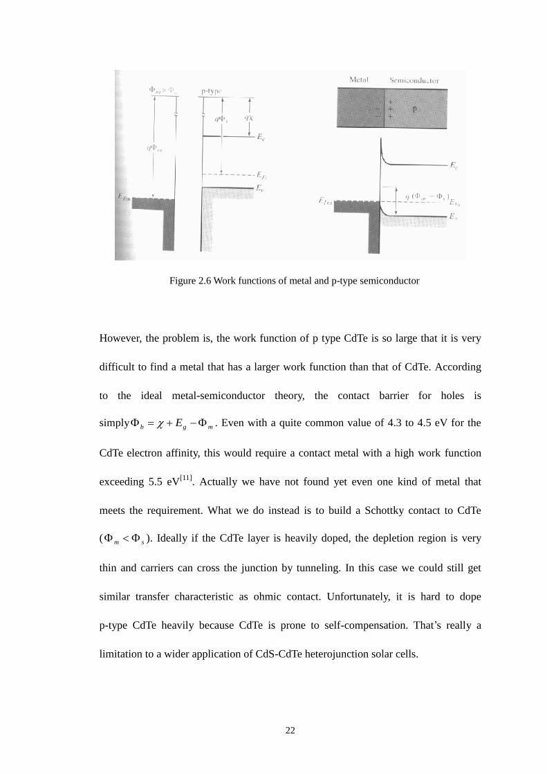
22
Figure 2.6 Work functions of metal and p-type semiconductor
However, the problem is, the work function of p type CdTe is so large that it is very
difficult to find a metal that has a larger work function than that of CdTe. According
to the ideal metal-semiconductor theory, the contact barrier for holes is
simply mgb E . Even with a quite common value of 4.3 to 4.5 eV for the
CdTe electron affinity, this would require a contact metal with a high work function
exceeding 5.5 eV[11]
. Actually we have not found yet even one kind of metal that
meets the requirement. What we do instead is to build a Schottky contact to CdTe
( sm ). Ideally if the CdTe layer is heavily doped, the depletion region is very
thin and carriers can cross the junction by tunneling. In this case we could still get
similar transfer characteristic as ohmic contact. Unfortunately, it is hard to dope
p-type CdTe heavily because CdTe is prone to self-compensation. That‟s really a
limitation to a wider application of CdS-CdTe heterojunction solar cells.

23
Production of large CdS-CdTe thin film solar cell modules is also limited by the low
efficiency of the photovoltaic process compared with silicon-based solar cells. Large
commercial modules only reach values of approximately 9%[12]
. One of the major
reasons for this poor performance is the presence of deep defects in the CdTe absorber
layer. These defects can capture the charge carriers generated by the photovoltaic
energy conversion, resulting in a decrease of output current, a loss in the open circuit
voltage and thus a lowering of the cell‟s efficiency. The effective value of the
CdS-CdTe p-n junction reverse saturation current density J0 increases with forward
bias due to the large trap density in its intrinsic region. This is what we do not want.
According to
L
AkTqV JeJJ )1(0 (2.4)
where A represents diode ideality factor which is 1 in the case of ideal silicon p-n
junction. From this we get a transformation of the formula:
1ln
0J
J
q
AkTV L
oc (2.5)
Thus if J0 increases with forward bias, Voc will decrease greatly, which is opposite to
what we would like it to be.
Last, people believe that the CdS-CdTe solar cell fabrication process is to some
degree not so healthy because we need to use CdCl2, which is toxic, to treat both CdS
and CdTe layers to achieve a high open circuit voltage. Cadmium chloride (CdCl2) is
24
used in the annealing induced activation of polycrystalline CdTe-CdS solar cells, and
this step is crucial in the device fabrication process. It was established that CdCl2
treatment leads to a grain growth and a passivation of the grain boundaries in the
CdTe active layer[13]
. It also promotes the formation, by inter-diffusion, of CdTe1-xSx
at the CdTe-CdS interface and reduces recombination in these devices[14]
. In fact, CdS
and CdTe are not toxic only because they are insoluble and any solution which
contains Cd+ may be toxic. So researchers are keeping looking for new procedures or
new materials that could somehow refine or replace the CdS-CdTe solar cell
fabrication process.
Copper indium diselenide (CIS) is another very promising absorber material among
all those thin film absorbers. High performance CdS/CIS based solar cells with an
efficiency of 19.5% have been reported[15]
on the laboratory scale and 10.3% over
large surface of 3860 cm2[16]
. Molybdenum (Mo) is usually used as the contact
material for CIS because it forms non-rectifying ohmic contact with CIS. So far the
most efficient CIS based solar cells are almost all made by vacuum coevaporation of
the three elements[17]
. And they generally apply a structure of glass/Mo/CIS/CdS/ITO
which is called the front wall structure[18]
. A reverse structure which is so named back
wall structure of glass/ITO/CdS/CIS/Mo is also adopted by some research groups[19]
.
With the back wall structure, people have achieved an efficiency of 5.0% by spray
technology[20]
and 8.1% by coevaporation[21]
.

25
The chalcopyrite CIS material system has been studied in detail in only the relatively
recent past, having first shown greater than 10% AM1.5 efficiency in 1981[22]
. Since
that time, many companies have announced plans to commercialize CIS-based
photovoltaics modules, but all were unsuccessful until Siemens Solar Industries (SSI),
introduced a CIS-based photovoltaic product in 1999[23]
. In addition to SSI, other
process labs currently studying CIS for academic purposes or in support of potential
(terrestrial or space) commercialization include the National Renewable Energy Lab
(NREL), Uppsala UniversityLPE, the Institute for Energy Conversion (IEC)
(University of Delaware), Matsushita, Energy Photovoltaics, Inc. (EPV), and Showa
Shell[22]
.
The realization of a commercial CIS product has been much slower than anticipated
because many of the processes used for fabrication of thin film polycrystalline
materials are quite complex. In particular, analytical instrumentation needed to
monitor the rate of materials deposition is lacking, and it has proved difficult to
maintain the requisite uniformity in deposited species across large areas[22]
.
Further, there is a lack of scientific understanding about many basic materials
properties of CIS films, especially those which control device performance, which
makes engineering of fabrication equipment particularly difficult. In the past, most
research activities have focused on how to provide the most efficient device fastest
instead of on how best to understand the fundamental materials system[22]
. The
26
problem has been compounded by the fact that very little research has been done on
chalcopyrite material systems such as CIS outside of the photovoltaics community, in
contrast to silicon and some III-V materials which have been studied extensively for
microelectronics applications, for example[24]
. Significant materials and electrical
engineering issues remain unresolved for CIS and its alloys. These include the
unknown nature of “primary materials factors” (such as phases, defects, impurities,
etc) and of the current-collecting barrier (homojunction vs. heterojunction)[25]
. An
example of an unknown material property is grain size, a quantity which may have a
significant impact on device performance. The size of features observed in SEM
images of CIS films is often quoted as being indicative of grain size, but there is no
fundamental reason why this should be the case. Diffraction techniques are instead
needed to determine grain size for CIS[23]
.
Other unresolved issues for CIS include the need for sufficiently detailed, predictive
fabrication process and device performance models, as well as the need for material
improvements in all device layers (absorber, contacts, etc). All of these issues are to
some extent being addressed by various research and manufacturing organizations,
but all remain open questions to date[23]
.
2.2.3 Organic solar cells
Organic photovoltaic devices are designed to fill the low-cost, low power niche in the
solar cell market[26]
. Recently measured efficiencies of solid-state organic cells are
27
close to 5%. In this type of solar cells, bound electron-hole pairs, which are named
excitons, are formed in organic semiconductors on photo-absorption. In the organic
solar cell, the exciton must diffuse to the donor-accepter interface for simultaneous
charge generation and separation. This interface is critical as the concentration of
charge carriers is high and recombination here is higher than in the bulk.
An important difference to inorganic solid-state semiconductors lies in the generally
poor (orders of magnitudes lower) charge-carrier mobility in these materials[27]
, which
has a large effect on the design and efficiency of organic semiconductor devices.
However, organic semiconductors have relatively strong absorption coefficients
(usually >=105 cm
-1), which partly balances low mobilities, giving high absorption in
even <100 nm thin devices. Another important difference to crystalline, inorganic
semiconductors is the relatively small diffusion length of primary excitons in these
rather amorphous and disordered organic materials[28]
. These excitons are an
important intermediate in the solar energy conversion process, and usually strong
electric fields are required to dissociate them into free charge carriers, which are the
desired final products for photovoltaic conversion. This is a consequence of exciton
binding energies usually exceeding those of inorganic semiconductors[29]
. These
features of organic semiconducting materials lead generally to devices with very
small layer thicknesses of the order <=100 nm[30]
.
Most of the organic semiconductors are hole conductors and have an optical band gap

28
around 2 eV, which is considerably higher than that of silicon and thus limits the
absorption of the solar spectrum to a great extent. Nevertheless, the chemical
flexibility for modifications on organic semiconductors via chemical synthesis
methods as well as the perspective of low cost, large-scale production drives the
research in this field in academia and industry[30]
.
Excitonic solar cells have different limitations on their open-circuit photo-voltages
due to these high interfacial charge carrier concentrations, and their behavior cannot
be interpreted as if they were conventional solar cells. The ultimate aim for organic
solar cells is to become a commercial reality[26]
.
Among all those organic materials, Phthalocyanines (Pcs) have attracted lots of
attention as a hole transport layer[31]
. Phthalocyanines show promising
photoconductive and photovoltaic responses and hence have been widely used in
Schottky barrier cells[32]
as well as multilayer solar cells[33]
. Due to a large series
resistance, low fill factor and incomplete coverage of the solar spectrum, the power
conversion efficiency of the Schottky barrier cells for AM1 solar radiation is typically
low[34]
. The efficiency is higher for lower incident light powers or monochromatic
excitation. The reported results in the literature for the phthalocyanine Schottky
barrier cells are in poor agreement with one another. The open-circuit voltage ranges
from several mV[35]
to more than 1 V[25]
. Short-circuit currents in the range from nA[36]
to uA[37]
have been reported. The reported power conversion efficiencies for white
29
light are 0.001% for CuPc, 0.00006% for FePc, and 0.00013% for CoPc[38]
. For
monochromatic low-power excitation, power conversion efficiencies of
phthalocyanine Schottky cells can be as high as 6%[39]
or even 14%[32]
.
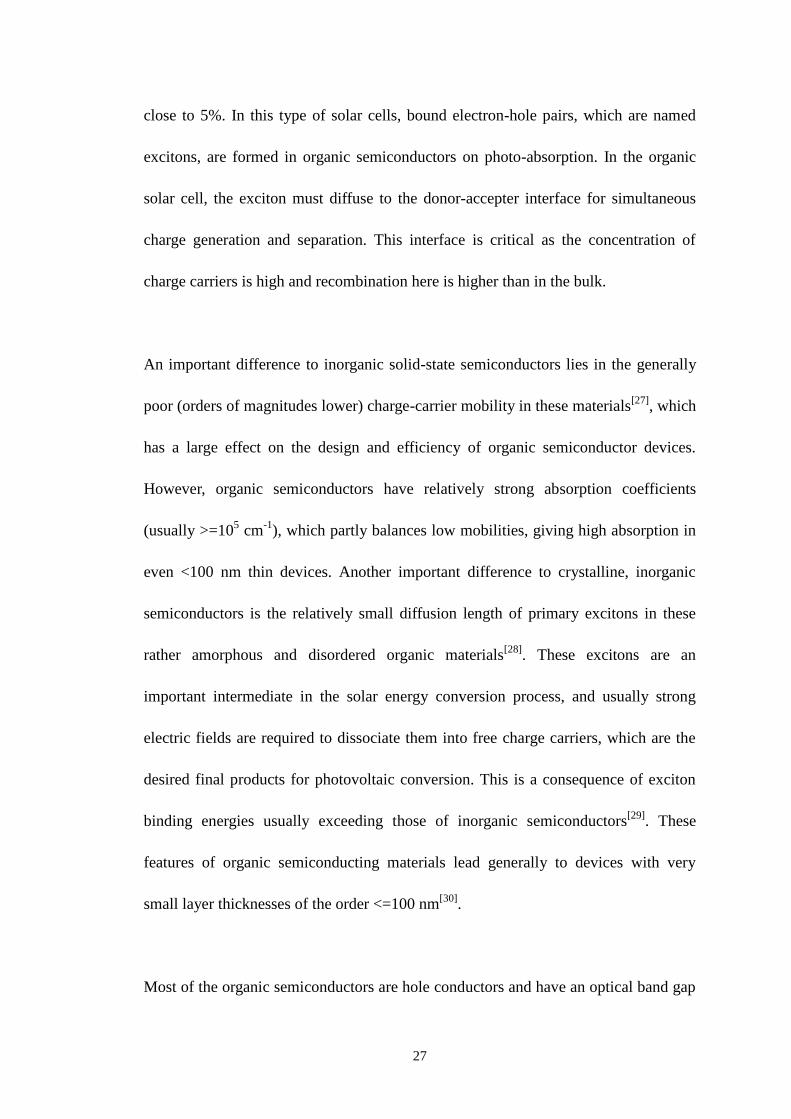
A typical structure of CuPc based organic solar cells is sketched in Figure 2.7[25]
. Also
an open circuit voltage of 1.15 V was achieved with this single-junction
CuPc/PTCBI/Al device structure by our group.
Figure 2.7 Configuration of CuPc-based solar cell with Al electrode
Despite of the thin PTCBI layer between CuPc and Al contact, the dominant junction
was modeled as the Schottky diode between the CuPc layer and aluminum because
the thin PTCBI layer was thought to be entirely incorporated into the CuPc, which
described as the modified CuPc layer as is shown in Figure 2.8[25]
. Since the build-in
potential Vbi must be larger than the observed open-circuit voltage, it is easy to
conclude that those electrodes with small build-in potential cannot provide high Voc

30
even though their current can be much higher than Al electrode. This is quite different
from those homojunction or heterojunction solar cells because the major junction now
is the metal-semiconductor Schottky diode.
Figure 2.8 Energy band diagram of CuPc-based solar cell with Al electrode
Despite of the high open circuit voltage, the current density is so low and the fill
factor is not good, either. These in combination result in a relatively very low
efficiency and the reasons have been discussed before. Nevertheless, organic
materials based solar cells are still attracting many researchers for its low cost process
and undergoing great improvement. They are sharing the market with those inorganic
solar cell producers.
2.2.4 Other types of solar cells
There are some other types of solar cells such as dye-sensitized solar cells and
31
multijunction solar cells. The dye-sensitized solar cells are mostly composed of a
nano-porous layer of titanium dioxide particles, covered with a molecular dye that
absorbs sunlight[40]
. The titanium dioxide is immersed under an electrolyte solution,
above which is a platinum-based catalyst. In the dye-sensitized solar cell, the bulk of
the semiconductor is used solely for charge transport, and the photoelectrons are
provided from a separate photosensitive dye. Charge separation occurs at the surfaces
between the dye, semiconductor and electrolyte[40]
. The highest efficiency achieved so
far by this type of solar cell is about 11%[41]
. Although it is not as efficient as many
other types of solar cells, it has an impressive performance in the scenario of low light
intensity and poor cooling system. It also has a great advantage in terms of low cost in
fabrication.
Multijunction solar cells are developed for satellite power applications where the high
cost is offset by the weight savings offered by the higher efficiency[42]
. They now
have terrestrial applications in concentrated photovoltaics. The most commonly used
multijunction solar cell structure is an array of three layers connected in series,
namely gallium indium phosphide (GaInP), gallium arsenide (GaAs), and germanium
(Ge). Sunlight with photon energy larger than the bandgap of GaInP will be absorbed
in the first layer (GaInP). Photons with less energy will be absorbed in the second
layer (GaAs), leaving the rest long-wavelength photons been absorbed in the third
layer (Ge), thus making the most use of the incoming sunlight. The highest efficiency
achieved so far for this type of solar cell is about 40.8% by National Renewable

32
Energy Laboratory (NREL) [42]
. This type of solar cells has the highest conversion
efficiency, however, the fabrication cost is also the most expensive one.
33
3. Advantages of Nano-structured Solar Cells
3.1 Definition of nanotechnology
The term of „nanotechnology‟ was firstly introduced by K. Eric Drexler in his book
“Engines of Creation” in 1986[43]
. Nanotechnology is used to refer to any process or
product that involves sub-micron dimensions, but a more concise definition is any
fabrication technology in which objects are built by the specification and placement of
individual atoms or molecules or where at least one dimension is less than 100 nm.
Since early 1990s, research interest in nanotechnology has grown rapidly and many
governments are now funding nanotechnology-related projects. These range from
nano-robots to new high-performance materials and nano-scale electronics.
3.2 Application of nanotechnology in solar cell development
Recently, nano technology has been applied to solar cell development to further
increase the efficiency. Nano technology could be used to tailor the bandgap of any
material that is used for fabrication of solar cells due to quantum confinement effect.
For examples, in CdS-CIS heterojunction solar cells, the CdS layer, which has energy
gap of 2.5 eV in normal condition, can broaden its bandgap to 3.5 eV in nano
structure. Since we want the light to totally pass through CdS layer and be absorbed in
the CIS layer near the junction, we could take advantage of this quantum effect,
making wider bandgap CdS layers to pass the light. To be more detailed, blue light
has the wavelength of 0.45 um which results in a 2.8 eV energy packet for its photons
according to

34
cE
. (3.1)
That is to say, nano structure of CdS passes the blue light which normal structure of
CdS cannot pass. Therefore, transparency is greatly improved and major absorption
occurs near the junction which means higher efficiency can be achieved. On the other
hand, we could also tailor the absorption layer into proper bandgap for higher build-in
voltage. Bulk CIS has a bandgap of 1.05 eV, which could be increased to the perfect
bandgap of 1.5 eV for solar cell application in nano size. Besides, more materials
could be considered as substitutes for window or absorber layers. At the same time,
we can take advantage of their unique electric or optical characteristics.
Other advantages of utilizing nanotechnology for solar cell development include
increasing the light path inside the absorber layer. If the diffusion length of generated
carriers is larger than the film thickness, most of the minority carriers can be collected.
Thus it is required that the absorber layer is thin enough for photogenerated carriers to
diffuse to depletion region and be swept across before they get recombined. However,
this layer cannot be infinitely thin because that will leave most photons pass through
the absorber layer without being absorbed. So the best way is to somehow tune the
structure and make the light path longer than carrier path. In fact, if the optical length
is larger than the inverse of the absorption coefficient, most light will be absorbed.
Intuitively, smaller size particles lead to more scattering of light and increased surface
area. In such case, light is more likely to scatter and reflect among nano structures
35
when passing through the solar cell which will result in improved absorption
coefficient.
Researchers have shown that more than 96% of incoming sunlight can be absorbed
within less than 5% device area of silicon nanowires of the same thickness[44]
. In this
manner, the material cost can be dramatically reduced at the cost of a more
complicated device structure. It has also been demonstrated that
nanowires/nanopillars based device can largely reduce the surface reflection of
incoming light[45]
, thus saving the cost for an anti-reflective layer.
Anodic aluminum oxide (AAO) is now widely used in many research fields[46]
as well
as industry applications[47]
due to its highly ordered cylindrical pores. What‟s more
attracting is that the pore diameter and length can be tuned easily for different
requirements by simply changing the acid concentration, applied voltage and
anodization time[48]
. The mechanism behind has been well studied for half a century[49]
and remarkable success has been achieved in both fabricating[50]
and understanding[51]
the structure.
Synthesis of nanowires inside the AAO templates is of great interest and has been
attracting more and more attention recently[52]
. Grain size of above 1 um is generally
attained by normal thin film preparation methods, such as electrodeposition,
evaporation and spray-coating[53]
. However, with the help of AAO templates, the
36
grain size of nanowires can be limited to several tens of nanometers or even less by
properly controlling the pore size[54]
. Many kinds of nanowires have been successfully
fabricated inside the AAO pores, including metals[55]
and semiconductors[56]
. And our
nano-structured solar cells design and simulation will be based on the AAO templates
and nanowires inside.
3.3 Simulation of efficiency enhancement in nano CdS-CdTe solar cells
For a quantified estimation of how much more efficiency can be achieved by utilizing
semiconductor nanowires, here we perform a simulation on nano-CdS / bulk CdTe
heterojunction solar cells as an example. As mentioned before, the nanowire (NW)
CdS layer has higher transmittivity than the traditional planar CdS window layer. It
has been observed by us and by several other research groups[57-58]
that the absorption
peak of CdS nanowires is shifted towards the blue region, compared with bulk CdS.
For our CdS nanowires, the optical absorption edge lies at a wavelength of 480 nm[58]
instead of the 512 nm for the traditional thin film CdS case. This enhances the number
of sunlight photons incident on the CdTe absorption layer, and increases the
light-generated current and the overall efficiency of solar cell.
In order to calculate the improvement in the efficiency, the light generated current
density for the junction was calculated. The following equations were used to obtain
the current density for the neutral region within the n-CdS material ( ), the current
density for the depletion region ( ), and the current density for the neutral region
37
within the p-CdTe material ( ).
The generation rate of electron-hole pairs at a distance x from the solar cell surface (in
this case, the interface between i-SnO2 and CdS) for a specific incident wavelength λ
is given by
(3.2)
where α(λ) is the absorption coefficient, ϕ(λ) is the number of incident photons per
unit area per time per wavelength, and R(λ) is the fraction of reflected photons.
Under low-level injection, the one-dimensional, steady-state continuity equation for
holes in the CdS layer is given by
(3.3)
where
(3.4)
Assuming the electric field in the n-type region can be neglected, we have
(3.5)
Solve this equation and apply the boundary conditions

38
at x = 0 (3.6)
where Sp is the surface recombination velocity, and at the depletion edge, the excess
carrier density is small due to the electric field in the depletion region, thus
at x = xj (3.7)
Therefore, the resulting photocurrent density of holes at the depletion region edge is
given by
(3.8)
Similarly, the photocurrent density of electrons is
(3.9)
39
And the photocurrent density in the depletion region is simply
(3.10)
Here is the elementary charge, is the photon flux density at the surface of
CdS (This value was extracted from the solar spectrum provided by NREL), is
the photon flux density at the junction edge in CdTe layer, is the reflected
fraction of the incident photons at the surface of CdS, is the reflected fraction
of the incident photons at the junction (for our simulation, the reflection is neglected,
i.e. reflection fraction R = 0), is the absorption coefficient for CdS, is
the absorption coefficient for CdTe, is the diffusion length for holes in n-CdS,
is the diffusion length for electrons in p-CdTe, is the surface recombination
velocity of holes in the n-CdS/metal junction, is the surface recombination
velocity of electrons in the p-CdTe/metal junction, is the diffusion coefficient of
holes in n-CdS, is the diffusion coefficient of electrons in p-CdTe, is the
distance from the surface of CdS to the beginning of the depletion region, is the
thickness of the CdS, is the distance from the surface of CdS to the end of the
depletion region (junction edge in CdTe, the depletion region width was assumed to
be 2 um), and is the thickness of CdS plus the thickness of CdTe.
The efficiency is normally calculated with the equation:
(3.11)
Where
40
(3.12)
In a practical CdS-CdTe solar cell, the photocurrent generated in the CdS layer can
hardly be collected due to its high surface recombination rate, thus has little
contribution to the light current. This is in agreement with our simulated result, where
the photocurrent generated in the CdS layer Jp = 1.4 x 10⁻⁴
mA/cm2, which is far
smaller than the current generated in the depletion region Jdr (usually greater than 20
mA/cm2 ).
Also the photocurrent generated in the neutral CdTe layer is small because the
depletion region in CdTe layer is usually long enough to absorb most incoming
sunlight, leaving a very small fraction of photons being able to reach the neutral
region in CdTe layer. In our simulation results, this is also shown by giving the value
of Jn = 0.14 mA/cm2. Thus, the major contribution of the light current comes from the
photocurrent generated in the depletion region Jdr.
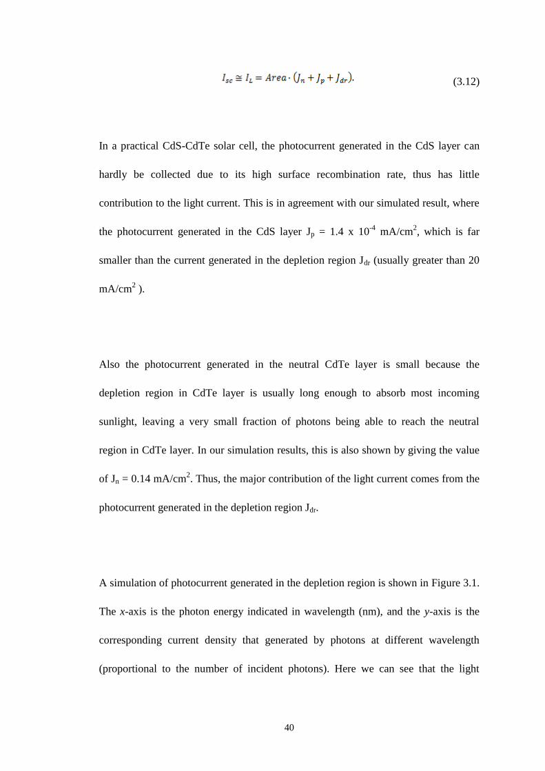
A simulation of photocurrent generated in the depletion region is shown in Figure 3.1.
The x-axis is the photon energy indicated in wavelength (nm), and the y-axis is the
corresponding current density that generated by photons at different wavelength
(proportional to the number of incident photons). Here we can see that the light
41
generated current density is larger at λ < 500 nm due to the absorption edge shift in
CdS nanowires, especially in the range of 480 ~ 500 nm.
300 400 500 600 700 800 900 10000
1
2
3
4
5
6
7
8x 10
-5
Wavelength (nm)
Photo
curr
ent
density (
A/c
m2)
Enhanced photocurrent due to absorption edge shift
Bulk CdS
Nano CdS
Figure 3.1 Simulation of photocurrent enhancement due to absorption edge shift in CdS NW
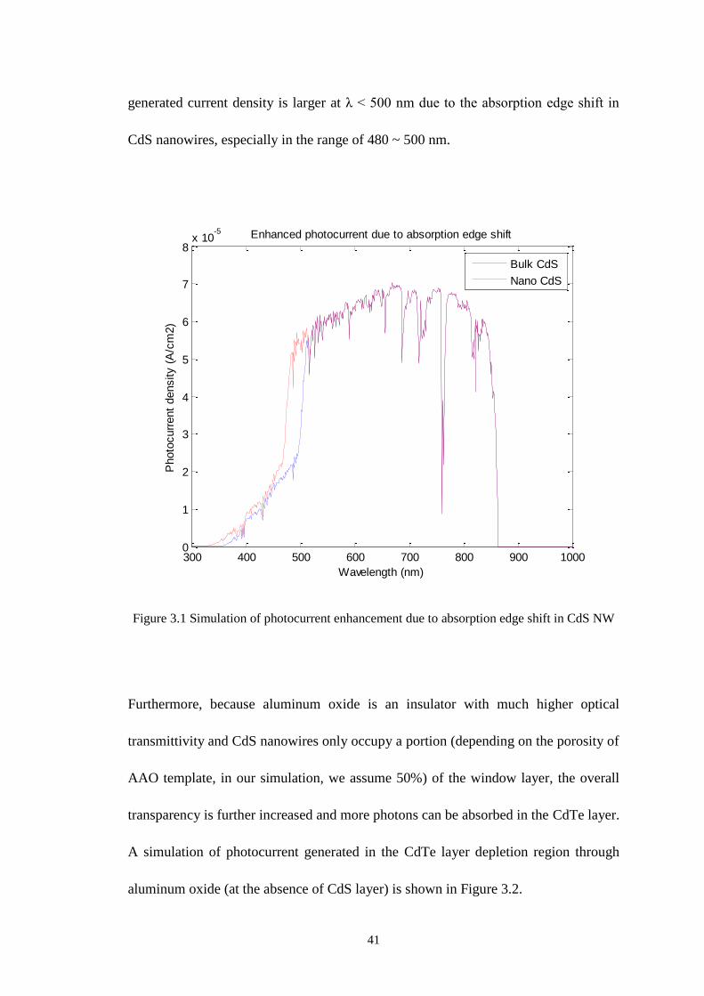
Furthermore, because aluminum oxide is an insulator with much higher optical
transmittivity and CdS nanowires only occupy a portion (depending on the porosity of
AAO template, in our simulation, we assume 50%) of the window layer, the overall
transparency is further increased and more photons can be absorbed in the CdTe layer.
A simulation of photocurrent generated in the CdTe layer depletion region through
aluminum oxide (at the absence of CdS layer) is shown in Figure 3.2.
42
Figure 3.2 Simulation of photocurrent generated in CdTe in the absence of CdS layer
Calculation results reveal that for a CdS layer thickness of 100 nm (both for planar
and nano structure), the light generated current gain is about 12%, from 23.7 mA/cm2
to 26.6 mA/cm2. This gain will further increase as the thickness of CdS layer
increases (more advantageous for thicker CdS layer). For example, in our fabricated
device which will be described in a later section, a thickness of 200 nm was used for
the nano CdS layer. Simulation showed that for 200 nm CdS layer, the photocurrent
gain is 17%, from 22.4 mA/cm2 to 26.1 mA/cm
2.
43
In another word, the number of useful photons reaching the depletion region in CdTe
absorption layer will be 17% higher for the AAO embedded NW-CdS window layer
(with an absorption edge at a wavelength of 480 nm and thickness of 200 nm) than for
the traditional CdS window layer (with an absorption edge at a wavelength of 512 nm
and thickness of 200 nm). Thus a 17% improvement in short-circuit current density
(Jsc) can be expected.
Besides that, in our device configuration, the CdS-CdTe interface has less junction
area than in case of traditional thin film solar cells because CdS only forms junction
with CdTe at the top end of each CdS nanowire. The effect of this junction area
reduction on reverse saturation current is considered this way: If the reverse saturation
current is dominated by minority carriers drifting (pure crystal assumption), then
according to
(3.13)
And for an n+-p junction as in our CdS-CdTe heterojunction case, this current is
dominated by the electrons drifted from the depletion region edge in the p-CdTe layer,
which has essentially no difference from a bulk CdS-CdTe structure because there is
no area change in the CdTe layer. On the other hand, if the reverse saturation current
is dominated by interface recombination process, in which case the number of

44
interface states are directly proportional to the interface area, then the reduction of
junction area is expected to result in smaller effective reverse saturation current (I0)
and hence a higher open circuit voltage (Voc) than in the traditional thin film CdS case,
as quantified by the equation below[59]
,
(3.14)
Note that even though the junction area is reduced substantially, the effective area for
light absorption remains the same, because those photons which pass through the
aluminum oxide instead of CdS will still get absorbed in the CdTe layer. Actual
improvement in the open circuit voltage will depend upon the ratio of the optical area
and the junction area and the dark current flow mechanisms prevailing at the
CdS-CdTe interface, characterized by the effective value of the diode ideality factor,
A, in above equation. As an example, for the case where the planar optical area is two
times the planar junction area (50% porosity) and A = 4, a traditional solar cell with a
Voc of 850 mV will reach a Voc of 922 mV with our NW-CdS design, an improvement
of 8.4% .
Since the power conversion efficiency of the solar cell is proportional to the product
of Jsc and Voc, a 17% improvement in Jsc and 8.4% improvement in Voc translate into a
26.8% improvement in power conversion efficiency. On the negative side, a slight
increase in the effective series resistance (RSE), and a corresponding decrease in the
45
fill factor (FF), can be expected because photo-generated electrons at the AAO/CdTe
interface need to travel an extra distance to get to the junction. For a circular CdS
nanowire of area A1 to collect the current from the bulk CdTe layer of area 4A1, the
effective bulk resistance of CdTe (RCdTe) will be twice the effective bulk resistance of
CdTe for the case of the traditional planar thin film CdS/CdTe solar cell. However,
the effect on RSE will be relatively small because RSE includes contributions from
other resistances like the contact resistance between CdTe and the top electrode,
which tend to be much larger and dominant.

46
4. Barrier-free AAO Templates on ITO Substrates
4.1 The widely use of AAO in template-assisted device fabrication
Template assisted fabrication of nanowires and nanorods has been widely used in
recent times. In particular, the anodic aluminum oxide (AAO) template, also known
as porous anodic alumina (PAA) template, is popular because of its highly ordered
structure[60-66]
. The AAO fabrication process and mechanisms of pore formation have
also been studied[67-68]
. Different types of nanowires have been produced and reported,
including metals[69]
, semiconductors[70]
and insulators[71]
. Various deposition
techniques have been used to acquire those nanowires, including electrodeposition
(ED)[72]
, chemical bath deposition (CBD)[73]
, and atomic layer deposition (ALD)[74]
.
There are two major types of AAO templates. In the first type, a pure aluminum foil,
generally with the thickness of several tens of microns to several hundreds of microns,
is the starting material. This kind of template is generally fabricated by two-step
anodization, which forms a highly ordered porous structure with high aspect ratio.
The aluminum foil is usually anodized all the way through, or the remaining part of
aluminum is etched off in CuCl2 solution, leaving an oxide barrier layer at the very
bottom of the pores, which is then etched off in phosphoric acid[75]
. The free-standing
open-pore structure may be directly used for deposition[76]
or a metal layer may be
deposited on one side of the pore structure[77]
, to serve as a substrate and an electrode.
Due to the handling problems associated with the free-standing template, this type of
47
AAO generally has a thickness of more than 10 microns. As a result, nanowires
fabricated in this fashion usually have a length of several tens of microns and a very
high aspect ratio[78]
.
The other type of AAO templates is grown on a certain substrate, such as silicon[79]
or
indium tin oxide (ITO)[80]
. The aluminum film is generally evaporated or sputtered on
top of the substrate, sometimes along with an interlayer such as titanium[81]
. In
comparison with the AAO fabricated from a pure aluminum sheet, this kind of
template is relatively short, its thickness ranging from a few hundreds of nanometers
to a few microns. The substrate usually functions as an electrode as well as a
mechanical support. On the other hand, the presence of this backside substrate makes
the removal of the residual aluminum oxide barrier layer an even harder challenge.
Most frequently, a simple phosphoric acid etch is used to remove the barrier layer[82]
.
Unfortunately, this method is effective only when an “inverted shape” barrier layer is
formed at the last stage of anodization, because, with that shape, the barrier layer
self-thins dramatically[83]
. Also, it was reported[84]
recently that this self-thinning
process could be implemented when an ultra-thin titanium interlayer of less than 0.5
nm was inserted between the ITO and the aluminum layers, prior to anodization.

48
However, it is difficult to deposit in a reproducible fashion, continuous films of
titanium as thin as 0.5 nm, and in the template assisted fabrication technology for
nanowires and nanorods, the aluminum oxide barrier layer, in general and
non-uniformity in barrier layer thickness, in particular, continue to be problems that
directly affect the growth rate, quality and uniformity of nanowires deposited
subsequently in the pores. These problems includes: 1) template cracking at the
electrolyte/air interface during anodization, 2) low transparency of AAO template on
ITO substrate, 3) low filling ratio of nanorods/nanowires, and 4) large variance in the
length of nanorods/nanowires. These issues are addressed here and the results are
applied successfully to the case of CdS nanowires deposited inside the pores.
4.2 Description of experimental details
A commercially available ITO layer with an average thickness of 150 nm deposited
on 1 mm thick glass was used as the substrate. The glass/ITO substrates were cut into
1 inch by 1 inch pieces and cleaned in ultrasonic acetone and methanol and rinsed in
de-ionized (DI) water. They were then subjected to a plasma etch for 4 minutes for
further surface cleaning. Next, in a set of experiments, titanium layers with
thicknesses ranging from 0.5 nm to 50 nm were sputtered on ITO for comparison.
Annealing in air was performed for some of these samples at 400°C for up to 5 hours,
while other samples were not annealed. Then an aluminum layer was evaporated on
49
top of titanium or titanium dioxide by e-beam evaporation; thickness of aluminum
layer was varied in the range of 200 nm to 1000 nm.
These glass/ITO/Ti(TiO2)/Al samples were anodized in 0.3 M oxalic acid under
constant voltage condition until a current increase was observed. The anodization
currents for different types of samples were recorded for reference. The as-anodized
samples were immersed in 5% phosphoric acid for 1 hour in room temperature to
widen pores and partially remove the barrier layer. Then some templates were
subjected to a reactive ion etch (RIE) process for 5~20 minutes (depending on the
template thickness) to remove the barrier layer completely. Although BCl3 has been
used in the past, to etch off aluminum oxide in the RIE process, its etch rate is too
high (about 770 nm/min as was reported[85]
) to be precisely controlled.
Also the TiO2 layer beneath the barrier oxide is undesirable, once the Al film has been
properly anodized. It is inserted only for adhesion and passivation, and needs to be
removed before nanowire deposition for a better device configuration. Therefore, in
our case, pure argon gas was used for the non-selective etch process to limit the etch
rate at about 5 nm per minute. The following parameters were used for the
non-selective Ar ion etch process: gas: Ar; flow rate: 20 sccm; base pressure: 5 x 10⁻⁵
Torr; working pressure: 20 mTorr; RF power: 90 W and ICP power: 250 W.
50
The bombarded Al2O3 particles had nowhere to go, and accumulated at the wall and
bottom of pores; these particles were later dissolved in phosphoric acid by a post-RIE
wet etch for a few minutes. In the case of thicker templates, this RIE and wet etch
cycles were performed for several times at 10 minutes RIE and 5 minutes wet etch
intervals for each cycle, to prevent bombarded particles from blocking further etching.
CdS nanowires were electrodeposited, for comparative evaluation, into all types of
templates made by anodization as described above, for comparison. The electrolyte
was composed of 0.055 M CdCl2 and 0.19 M elemental sulfur, dissolved in 100 mL
dimethyl sulfoxide (DMSO) and heated up to 120°C as reported in reference[86]
. It is
believed that dc deposition can most effectively reveal the status presence or absence
of barrier layer. In other words, only those pores without any barrier layer can be
filled efficiently with nanowires under dc condition, and the uniformity of nanowires
indicates the uniformity of barrier layer removal.
For electrodeposition, a constant current density of 15 mA/cm2 was applied for
several seconds. The estimated growth rate was 30 nm per second. The same
condition was used for all electrodeposition process for a controlled comparison. To
reveal the overall filling status of the CdS nanowires, the AAO templates were
dissolved in 0.1 M NaOH solution for 10 minutes before imaging by scanning
electron microscope (SEM). Last, a gold layer of 80 nm thickness was evaporated on

51
top of the nanowires by E-beam evaporation, yielding Au/CdS nanowire Schotky
diodes.
4.3 Barrier layer study of AAO templates on ITO substrates
4.3.1 The mechanism of non-uniform barrier layer formation
A typical SEM image of AAO template (with 5 nm Ti interlayer) on ITO substrate
after phosphoric acid etching is shown in Figure 4.1[87]
.
Figure 4.1: A typical SEM image of AAO template on ITO substrate showing non-uniform
barrier layer thickness.
52
It is observed that some pores have no barrier layer while others have barrier layers
ranging in thickness from less than 10 nm to about 25 nm. A normal distribution with
an average thickness of around 15 nm was extracted for the observed barrier layer. It
is interesting to note that even neighboring pores can have barrier layers with
thicknesses differing by as much as 25 nm. This indicates that the process
non-uniformities exist within a sample, in addition to variations that may be found
between one sample and another. These non-uniformities can be caused by a series of
factors, including,
(i) The non-uniform deposition of sputtered titanium interlayer. Sputtered films can
have surface roughness of as large as 1.5 nm[88]
. This is not negligible considering that
we are depositing only a few nanometers of Ti layer. In fact, in our experimental
series, those samples with Ti thickness of less than 3 nm were not stable during
anodization. Some of them could be properly anodized, while others would crack at
the electrolyte-air interface, leaving a large area un-anodized (current already reached
zero). Although it was reported[84]
earlier that an AAO template with very thin barrier
layer can be fabricated on ultra thin Ti layer (0.5 nm), in our work, substantially
thicker titanium inter-layers seemed to be necessary. This could be related to fact that
in our experiments, much thicker aluminum films (up to 1000 nm) were anodized
while in Ref. 84, the aluminum film thickness was less than 200 nm. In any case, it
would be preferable to have a proper interlayer thickness that is suitable for a large
range of template thicknesses as will be discussed in the section below.
53
(ii) Non-uniformity in the process for the deposition of the aluminum film.
Evaporated Al films can have a reported surface roughness of around 10 nm[88]
.
Defects and impurities resulting from the evaporation process also play an important
role. Lower base pressure and deposition rate during evaporation process can be
expected to produce purer aluminum films, but complete elimination of defects and
impurities still remains a hard challenge.
(iii) Non-uniform electric field present in these samples during anodization. The
electric field has the highest value at the interface between the electrolyte and air.
This can be demonstrated by the following two facts. First, it was observed that, at the
end stage of anodization, the region near the interface of electrolyte and air became
transparent first, and then transparency propagated downwards, until the whole
sample became transparent. The entire process took several minutes and was
proportional to the Al film thickness, indicating that the fastest reaction (or the highest
field) occurred at the interface. Second, for those samples with a Ti thickness of less
than 3 nm, the crack always happened in the region next to the interface, as was
mentioned above. Nevertheless, nothing can be practically done to improve the
electric field. What we can do is to properly tune the Ti layer thickness to withstand
this field variation. In our fabrication procedure, a 5 nm thick Ti layer was adopted as
a standard for template fabrication, to provide enough process non-uniformity

54
tolerance. With this thickness, all samples (aluminum thickness from 200 nm to 1000
nm) could be properly anodized.
4.3.2 Study of anodization process
A sketch of typical current versus time plot as well as a real I-t curve monitoring the
anodization process of a Al(200nm)/Ti(5nm)/ITO/Glass sample is shown in Figure
4.2[87]
. This sample was taken out of the electrolyte after 420 seconds of anodization,
where a slight current rise was detected.
(a)

55
(b)
Figure 4.2: (a) A sketch of typical current versus time plot with five stages marked (b)
Example of an actual I-t curve used for monitoring the anodization process of a
Al(200nm)/Ti(5nm)/ITO/Glass sample.
Note that Fig. 4.2 was obtained for the case of a constant voltage anodization at 50V,
5°C with sample size of ~5 cm2. Five stages can be distinguished from the plot:
(1) At the first stage, initially the current was very high due to the high conductivity
of metal Al and the lack of any oxide layer. As the anodization started, aluminum
oxide layer formed on the top surface of the evaporated Al film, greatly increasing the
56
resistance, and the anodization current dropped dramatically. This can be called the
oxidation stage, and generally lasts for 20~30 seconds.
(2) During the second stage, the pre-formed oxide layer started to dissolve from some
random sites on the oxide surface and nano pores were initiated. This had an overall
effect of thinning the oxide layer, thus the resistance decreased and current increased
a bit. This can be called the dissolution stage, and lasts for a few minutes.
(3) In the third stage, the oxide formation process and dissolution process gradually
balanced each other and an equilibrium state was achieved. Also the pores started to
form an ordered structure by self-adjusting pore sizes and inter-pore spaces[89]
. The
anodization current was constant during this stage. Note that the time period of this
stage could range from a few seconds to several tens of minutes or even longer,
depending upon the thickness of the aluminum layer. This can be called the steady
stage. The three stages mentioned above commonly exist in all kinds of aluminum
anodization, but the following stage (stage 4) can be observed only when the whole
Al layer is consumed (either in anodization of Al deposited on top of a rigid substrate
or in a complete anodization of an aluminum foil), and stage 5 is unique for aluminum
films deposited on top of a conducting or semiconducting rigid substrate[84]
.

57
(4) At the beginning of the fourth stage, the anodization front, which is the Al2O3/Al
interface, reached the surface of the Ti under-layer. The remaining aluminum metal
was gradually consumed and the corresponding anodization current decreased and
finally approached a very small value close to zero. During this process, the film
gradually changed its color and finally became transparent if the titanium layer is thin
enough. Depending on the thickness of the Ti layer, the tail of this stage might be
extended from a few minutes to several hours. This can be called the consumption
stage. More details concerning what was actually happening during this stage will be
revealed later associated with stage five.
(5) In the fifth stage, the anodization current started to rise. Template destruction was
observed with the increasing of the current, so the anodization process was generally
stopped at the beginning of this stage. This can be called the destruction stage or
ending stage. An inverted barrier layer was commonly observed for samples stopped
at this stage. Hong-seok Seo et al believed that this formation of void beneath the
barrier layer was to accommodate the stresses created by volume expansion[90]
.
However, in our opinion, this is more likely to be due to the tiny oxygen bubbles
formed at the Al2O3/Ti interface. Our reasons are described below.
Volume expansion accompanies film anodization, and should be finished wherever
the Al is completely consumed, which is at the consumption stage (stage 4). However,
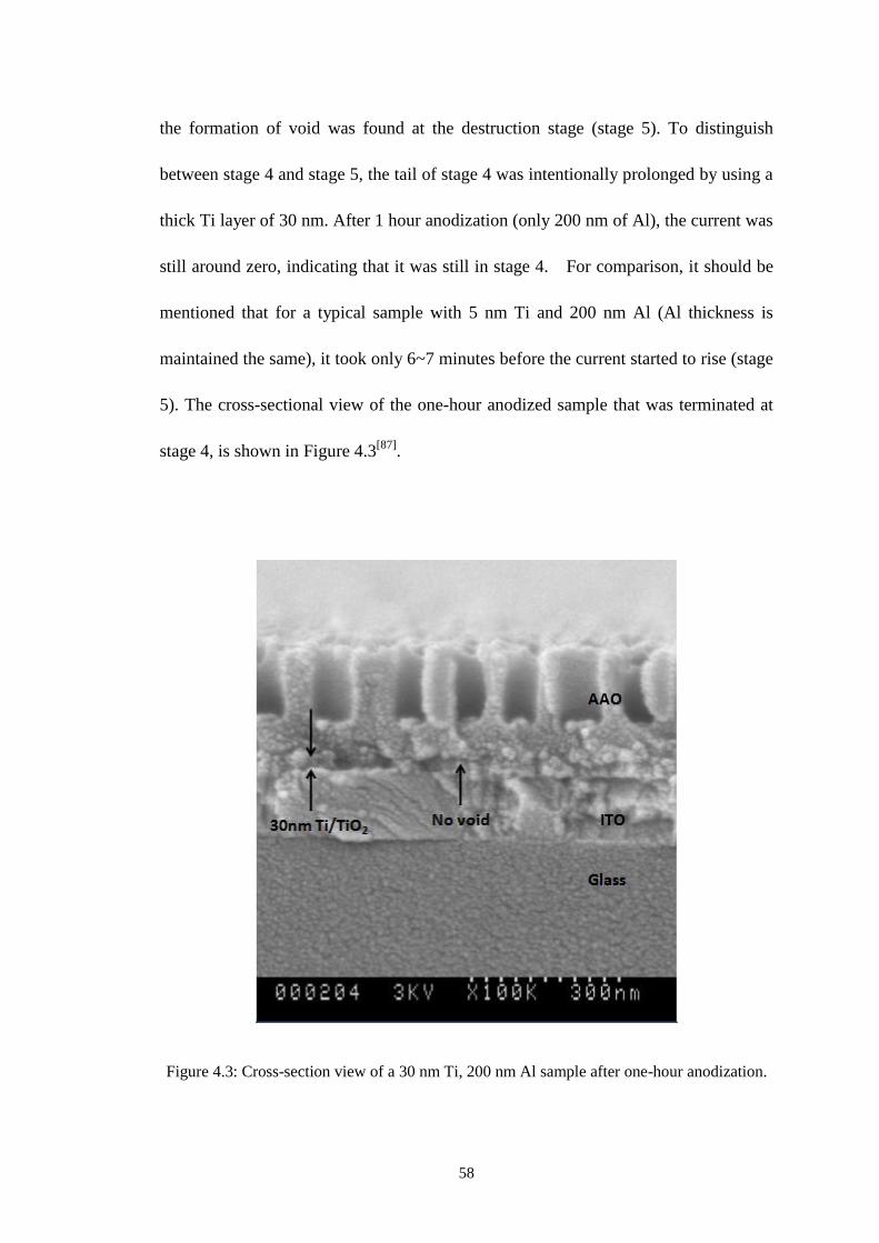
58
the formation of void was found at the destruction stage (stage 5). To distinguish
between stage 4 and stage 5, the tail of stage 4 was intentionally prolonged by using a
thick Ti layer of 30 nm. After 1 hour anodization (only 200 nm of Al), the current was
still around zero, indicating that it was still in stage 4. For comparison, it should be
mentioned that for a typical sample with 5 nm Ti and 200 nm Al (Al thickness is
maintained the same), it took only 6~7 minutes before the current started to rise (stage
5). The cross-sectional view of the one-hour anodized sample that was terminated at
stage 4, is shown in Figure 4.3[87]
.
Figure 4.3: Cross-section view of a 30 nm Ti, 200 nm Al sample after one-hour anodization.
59
It can be seen that no void structure is formed beneath the barrier layer and the shape
of the barrier is flat instead of inverted. In contrast, Fig. 4.1 was the cross-section
view of a typical 5 nm Ti, 200 nm Al sample taken out at the ending stage (stage 5),
from which voids can be easily detected at the bottom of almost every pore. Note that
in Fig. 4.1 the inverted barrier structure was not seen because it had already been
immersed in phosphoric acid for 1 hour for pore widening and the inverted shape had
been etched off. From the comparison between Fig. 4.1 and Fig. 4.3, the void
formation associated with current increase in stage 5 is more likely to be due to other
mechanisms, different from the volume expansion which finished at stage 4.
4.3.3 The effect of titanium layer in anodization
To better understand the non-uniformity in anodization process, we need to further
study as to what is actually happening during the anodization stage 4 and stage 5.
We will start from the anode reaction described in Ref. 89:
Al2O3 + n H2O → 2Al3+
+ 3O2-
+ n OH- + n H
+ (4.1)
This is the electric-field enhanced aluminum oxide dissolution reaction. Under
electric field, the Al3+
and H+ ions are ejected from the oxide surface immediately,
while the O2-
and OH- anions migrate through the oxide layer and reach the Al2O3/Al
60
interface, where the aluminum metal is oxidized. In the case where no Ti interlayer
was inserted, after the aluminum layer had been consumed (stage 4), the O2-
and/or
OH- anions touched the ITO electrode (positive polarity) and lost electrons, producing
tiny oxygen bubbles at the Al2O3/ITO interface. This process would create voids
between Al2O3 and ITO, and would thin the barrier layer; this would further increase
the electric field, pushing more anions into the interface. Such a positive feedback
process would produce a huge amount of oxygen at the interface and destroy the
template in a short time. This is the reason for the large current spike at the ending
stage, observed by our group as well as many other groups[69,84,88]
.
In the case where a Ti interlayer was used, things were different. When the
anodization process reached the Al/Ti interface, no more aluminum could be oxidized.
At that moment, however, the oxide barrier thickness had not been changed, thus the
electric field remained, pushing O2-
and/or OH- anions to the interface, where titanium
reacted with these anions and formed titanium dioxide:
Ti + 2O2-
→ TiO2 + 4e- (4.2)
Ti + 4 OH- → TiO2 + 2 H2O + 4 e
- (4.3)
From the view of process non-uniformity, we can say that this Ti interlayer was
capable of tolerating the oxygen evolution reactions (OER) to some extent. This is
61
critical to the proper anodization of the whole film. For those samples without the Ti
layer or with a too thin Ti layer, the OER is too fast to be controlled, quickly cracking
the template at the electrolyte-air interface, and leaving a large area un-anodized as
mentioned above. The tolerance of this Ti layer increased with the increase of Ti
thickness. In a further test, a sample with 30 nm Ti was anodized for as long as 5
hours and remained in stage 4.
However, a thick Ti layer is not preferred as it actually hinders the occurrence of stage
5 and prolongs the anodization process too much as described before. Typically, a 5
nm Ti layer is good enough to extend the tail of stage 4 to tolerate the anodization
non-uniformities associated with Al films, as thick as 1000 nm. After a few minutes,
the thin Ti layer was completely oxidized (locally saturated) and could not tolerate
any more O2-
and/or OH- anions. At that time, if the electric field is still strong enough
(depending on the thickness of these two oxide layers) to drive anions in, the anions
will lose electrons and form oxygen as they are supposed to according to the analysis
before. Voids thus formed would serve as a sign of the start of stage 5.
To further confirm the O2-
and/or OH- anions saturation mechanism in Ti layer, some
samples with 30 nm Ti were annealed in air at 400°C for 1 hour to convert Ti into
TiO2 before Al deposition. In contrast with the samples without air annealing, which
remained at stage 4 after 1 hour anodization (as was shown in Figure 4.3), these air
62
annealed samples stepped into stage 5 (signature current increase and template
destruction detected) after about 5 minutes anodization. To further extend this study,
some samples with the same Ti thickness were air annealed for 5 hours to completely
convert them into TiO2. These TiO2 saturated samples showed no OER tolerance. It
was, as if there were no interlayer at all. These facts confirmed that the local oxygen
saturation in Ti layer and oxygen evolution reactions were the real mechanisms
behind the formation of inverted barrier layer.
4.3.4 The effect of non-uniform barrier layer in nanowire electrodeposition
With the knowledge of what was actually happening during various anodization
stages, we looked more closely at the effects that could be expected to follow from the
non-uniform anodization and the remedies for these effects. Theoretically, due to the
non-uniform process, when the deepest pore (pioneer) reached stage 5, others might
still be in stage 4, 3, 2 or even 1. However, as was mentioned above, the process
non-uniformity generally did not exceed 2~3 minutes difference practically. Within a
reasonable range of Al layer thicknesses, the duration of the steady stage (stage 3), on
its own, would be longer than the anodization time associated with process
non-uniformity.
In other words, when the pioneer pore reaches stage 5, other pores would have
reached at least stage 4 or 3. And this situation can be further improved by applying a
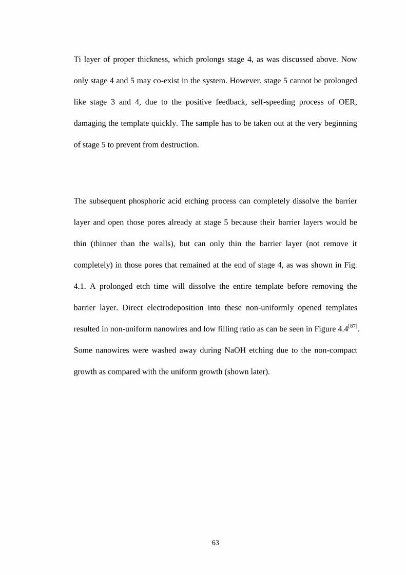
63
Ti layer of proper thickness, which prolongs stage 4, as was discussed above. Now
only stage 4 and 5 may co-exist in the system. However, stage 5 cannot be prolonged
like stage 3 and 4, due to the positive feedback, self-speeding process of OER,
damaging the template quickly. The sample has to be taken out at the very beginning
of stage 5 to prevent from destruction.
The subsequent phosphoric acid etching process can completely dissolve the barrier
layer and open those pores already at stage 5 because their barrier layers would be
thin (thinner than the walls), but can only thin the barrier layer (not remove it
completely) in those pores that remained at the end of stage 4, as was shown in Fig.
4.1. A prolonged etch time will dissolve the entire template before removing the
barrier layer. Direct electrodeposition into these non-uniformly opened templates
resulted in non-uniform nanowires and low filling ratio as can be seen in Figure 4.4[87]
.
Some nanowires were washed away during NaOH etching due to the non-compact
growth as compared with the uniform growth (shown later).
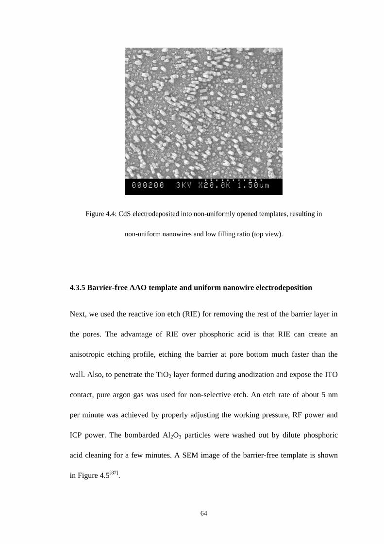
64
Figure 4.4: CdS electrodeposited into non-uniformly opened templates, resulting in
non-uniform nanowires and low filling ratio (top view).
4.3.5 Barrier-free AAO template and uniform nanowire electrodeposition
Next, we used the reactive ion etch (RIE) for removing the rest of the barrier layer in
the pores. The advantage of RIE over phosphoric acid is that RIE can create an
anisotropic etching profile, etching the barrier at pore bottom much faster than the
wall. Also, to penetrate the TiO2 layer formed during anodization and expose the ITO
contact, pure argon gas was used for non-selective etch. An etch rate of about 5 nm
per minute was achieved by properly adjusting the working pressure, RF power and
ICP power. The bombarded Al2O3 particles were washed out by dilute phosphoric
acid cleaning for a few minutes. A SEM image of the barrier-free template is shown
in Figure 4.5[87]
.
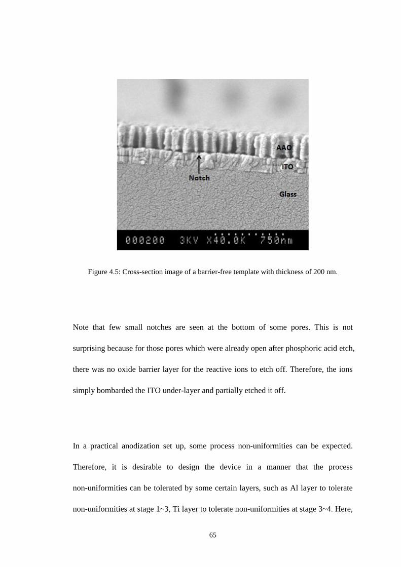
65
Figure 4.5: Cross-section image of a barrier-free template with thickness of 200 nm.
Note that few small notches are seen at the bottom of some pores. This is not
surprising because for those pores which were already open after phosphoric acid etch,
there was no oxide barrier layer for the reactive ions to etch off. Therefore, the ions
simply bombarded the ITO under-layer and partially etched it off.
In a practical anodization set up, some process non-uniformities can be expected.
Therefore, it is desirable to design the device in a manner that the process
non-uniformities can be tolerated by some certain layers, such as Al layer to tolerate
non-uniformities at stage 1~3, Ti layer to tolerate non-uniformities at stage 3~4. Here,
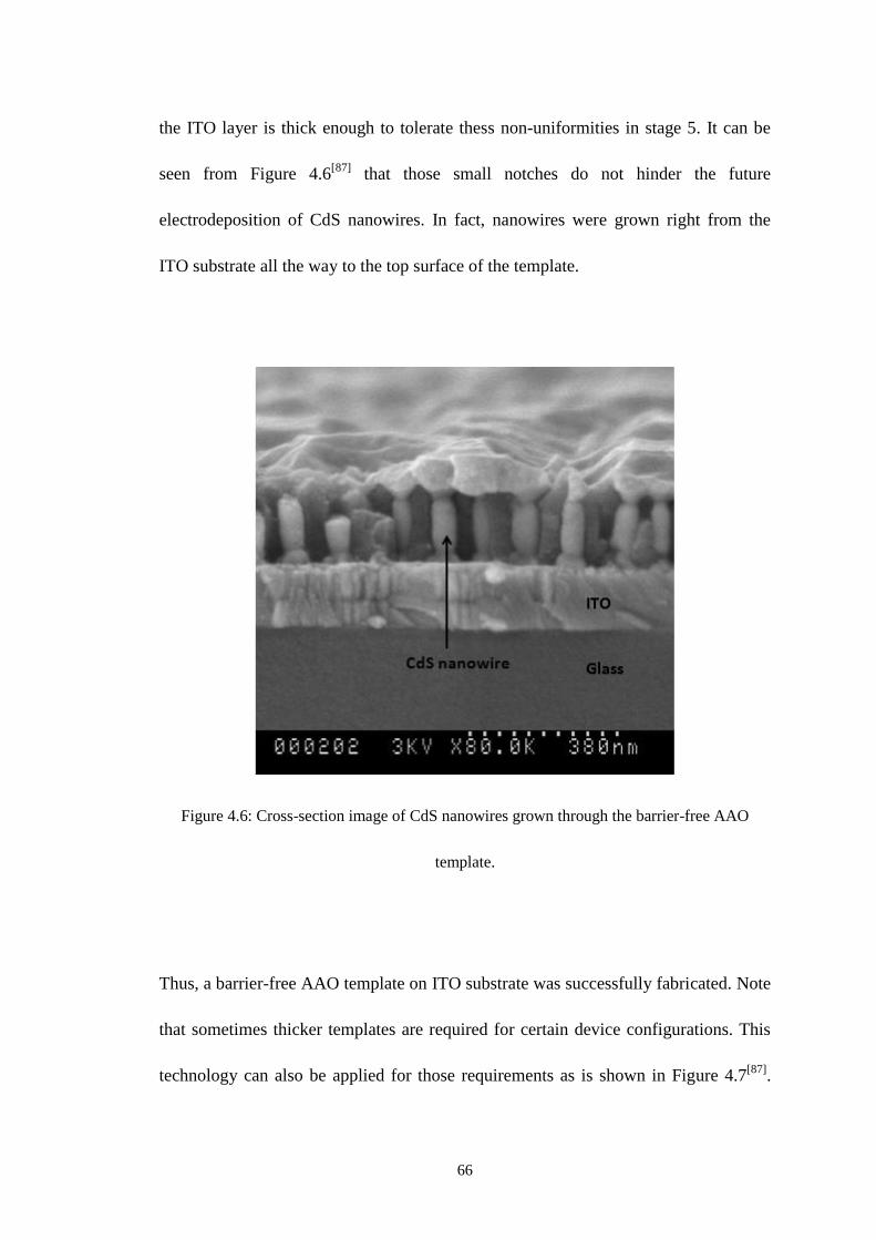
66
the ITO layer is thick enough to tolerate thess non-uniformities in stage 5. It can be
seen from Figure 4.6[87]
that those small notches do not hinder the future
electrodeposition of CdS nanowires. In fact, nanowires were grown right from the
ITO substrate all the way to the top surface of the template.
Figure 4.6: Cross-section image of CdS nanowires grown through the barrier-free AAO
template.
Thus, a barrier-free AAO template on ITO substrate was successfully fabricated. Note
that sometimes thicker templates are required for certain device configurations. This
technology can also be applied for those requirements as is shown in Figure 4.7[87]
.
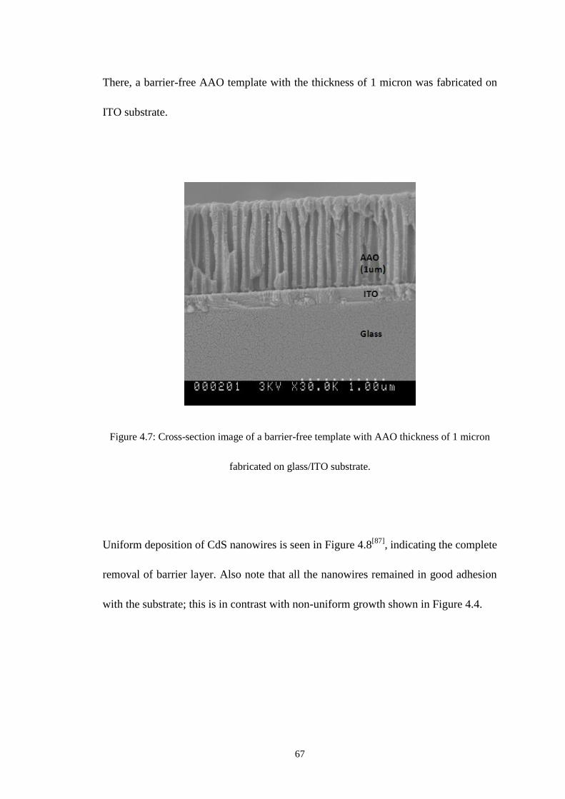
67
There, a barrier-free AAO template with the thickness of 1 micron was fabricated on
ITO substrate.
Figure 4.7: Cross-section image of a barrier-free template with AAO thickness of 1 micron
fabricated on glass/ITO substrate.
Uniform deposition of CdS nanowires is seen in Figure 4.8[87]
, indicating the complete
removal of barrier layer. Also note that all the nanowires remained in good adhesion
with the substrate; this is in contrast with non-uniform growth shown in Figure 4.4.

68
Figure 4.8: Uniform deposition of CdS nanowires into a barrier-free template. The template
was dissolved in NaOH for SEM imaging (top view).
In addition to the CdS nanowire example given here, this technique for barrier layer
free AAO template fabrication has applications in a wide variety of templated
nanostructured devices. The transmittance of such a template on ITO was measured to
demonstrate the capability of its application in electric-optical devices. As shown in
Figure 4.9[87]
, the transmittance of the AAO template on ITO is pretty close to the
ITO substrate itself.
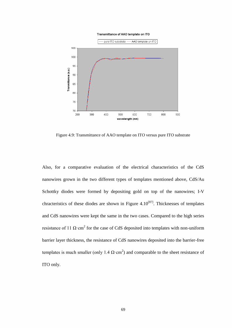
69
Figure 4.9: Transmittance of AAO template on ITO versus pure ITO substrate
Also, for a comparative evaluation of the electrical characteristics of the CdS
nanowires grown in the two different types of templates mentioned above, CdS/Au
Schottky diodes were formed by depositing gold on top of the nanowires; I-V
chracteristics of these diodes are shown in Figure 4.10[87]
. Thicknesses of templates
and CdS nanowires were kept the same in the two cases. Compared to the high series
resistance of 11 Ω·cm2 for the case of CdS deposited into templates with non-uniform
barrier layer thickness, the resistance of CdS nanowires deposited into the barrier-free
templates is much smaller (only 1.4 Ω·cm2) and comparable to the sheet resistance of
ITO only.
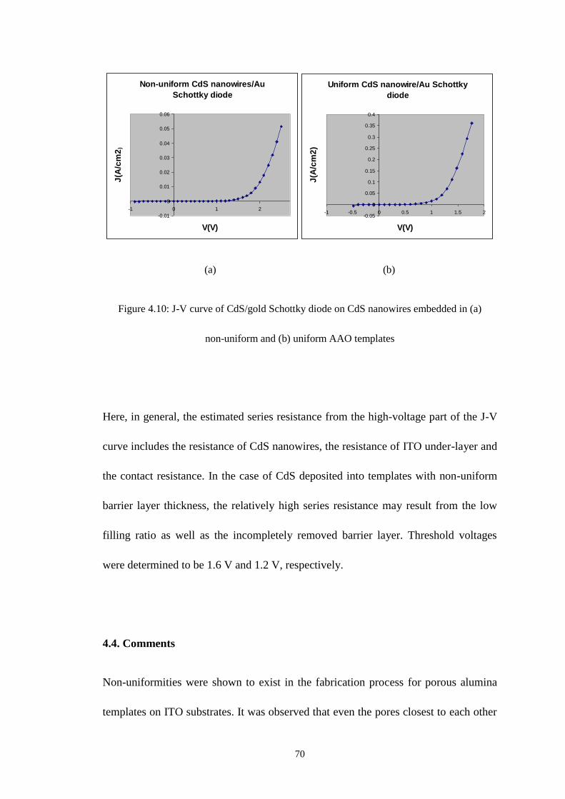
70
Non-uniform CdS nanowires/Au
Schottky diode
-0.01
0
0.01
0.02
0.03
0.04
0.05
0.06
-1 0 1 2
V(V)
J(A
/cm
2)
Uniform CdS nanowire/Au Schottky
diode
-0.05
0
0.05
0.1
0.15
0.2
0.25
0.3
0.35
0.4
-1 -0.5 0 0.5 1 1.5 2
V(V)
J(A
/cm
2)
(a) (b)
Figure 4.10: J-V curve of CdS/gold Schottky diode on CdS nanowires embedded in (a)
non-uniform and (b) uniform AAO templates
Here, in general, the estimated series resistance from the high-voltage part of the J-V
curve includes the resistance of CdS nanowires, the resistance of ITO under-layer and
the contact resistance. In the case of CdS deposited into templates with non-uniform
barrier layer thickness, the relatively high series resistance may result from the low
filling ratio as well as the incompletely removed barrier layer. Threshold voltages
were determined to be 1.6 V and 1.2 V, respectively.
4.4. Comments
Non-uniformities were shown to exist in the fabrication process for porous alumina
templates on ITO substrates. It was observed that even the pores closest to each other
71
could have their barrier layer thicknesses differ by as much as 25 nm. The potential
origins for this non-uniformity were traced to non-uniformities in Ti deposition, Al
deposition and the electric field in the device. The whole anodization process was
divided into five stages and reactions for each stage were provided.
A Ti interlayer with proper thickness can be used to mitigate the effects of
non-uniform anodization of stage 4 and before. On the other hand, too thick Ti layer
is not desirable as it actually hinders the occurrence of stage 5 and prolongs the
anodization process. Mechanism for voids formation beneath barrier layer is likely to
be the local oxygen saturation in Ti layer and oxygen evolution reactions when the O2-
and/or OH- anions are driven by electric field and come in contact with the electrode.
These hypotheses were confirmed by comparison of results from templates with
different Ti layer thicknesses and different annealing conditions.
Reactive ion etch (RIE) was used to mitigate against process non-uniformities after
stage 5 as well as to penetrate the remaining, unnecessary TiO2 layer. The ITO layer
was shown to be thick enough to tolerate the non-uniformity during RIE process, by
observing that CdS nanowires were grown right from the small notches created by
RIE. Barrier-free AAO templates with thicknesses ranging from 200 nm to 1000 nm
on ITO substrate were successfully fabricated and demonstrated by uniform filling of
CdS nanowires, in the AAO pores. The resistance of CdS nanowires deposited into

72
the barrier-free templates is very small (only 1.4 Ω·cm2) and comparable to the sheet
resistance of ITO only.
73
5. Nanostructured CdS – CdTe Solar Cells
5.1 New design of CdS – CdTe solar cell by nano engineering
Photovoltaic devices have been developed over the last few decades and several
absorber materials have been found to efficiently convert sunlight into electricity as
mentioned before. However, in the past ten years, improvement in the power
conversion efficiency for silicon based solar cells as well as for cadmium telluride
(CdTe) and copper indium gallium selenide (CIGS) based thin film solar cells has
been relatively small[91]
. This is because the fabrication process optimization is slowly
approaching its limit.
To further increase the solar to electric conversion efficiency, many researchers are
now exploring novel device designs involving nanostructured materials[92-93]
.
Several potential advantages of nano-structured cell design over the traditional thin
film configurations[94-95]
have already been demonstrated. Nanotechnology is believed
to be the most promising path to the next generation solar cells of high efficiency and
low cost. Although efficiency values achieved to date by nanostructured designs are
smaller than the values for the traditional solar cell designs, they are expected to
surpass the latter by wide margins as the new technology becomes more mature, and
the understanding of size effects becomes deeper.
74
Current state of art in nanostructured CdS-CdTe solar cells is reflected in the work of
Javey group who have shown that arrays of CdS nanopillars have much less light
reflectance than a planar film[96]
. Also, they have designed a 3D complex of CdS and
CdTe, made solar cells with CdS nanopillar arrays and CdTe interpenetrating each
other, and demonstrated a cell power conversion efficiency value of 6%[97]
. In terms
of the efficiency of power conversion, this cell had been the best so far among all
solar cells based on nanopillars, nanowires, nanodots, and nanorods. Here, we used
improvements in nanomaterials and in device configurations to achieve yet higher
power conversion efficiency in NW-CdS/CdTe solar cell devices. These studies are
described in the following sections.
In this chapter, we describe two novel device configurations for nano-structured
CdS/CdTe solar cells. These are illustrated in Figure 5.1 and are distinguished by the
red and blue arrows[98]
.

75
Figure 5.1: Flow chart of the newly designed fabrication process of CdS nanowires based
CdTe-CdS solar cells. Red arrow – Design A: CdS nanowires remained embedded in
nanoporous alumina (AAO) templates; Blue arrow – Design B: CdS nanowires were
free-standing.
In both cases, a nanoporous film of AAO is formed on top of the transparent electrode
and is used as a template for growing CdS nanowires in the pores. After the formation
of CdS nanowires, in the case of Design-A (red arrows), alumina film embedding the
CdS nanowires was left in place. In the case of Design-B (blue arrows), the anodic
aluminum oxide (AAO) template was removed, leaving behind freestanding CdS
nanowires.

76
Note that in some cases, a thin top layer of CdS can exist after electrodeposition of
CdS nanowires (NW) into the AAO template. Such a top layer would hinder the later
etching of AAO templates. Thus in Design B, thicker templates (~100nm thicker than
desired CdS nanowire length) were used but only the bottom 200nm of the pores were
filled with CdS to ensure the absence of the top CdS layer.
The advantages of applying a nano-structured window layer have been discussed
before in Chapter 3. Besides, both of these device designs have the following
advantages over the existing configuration suggested by Javey group:
1) In the device configuration of Javey group[97]
, the CdS layer is adjoined by an
opaque aluminum sheet, because the porous alumina (AAO) template is built from an
aluminum foil. Therefore, sunlight needs to be shined from the CdTe side, which, in
that case, is blocked partially by the top contact of gold and copper, resulting in a 50%
loss of incoming light[97]
. In our design, the AAO template is built directly on top of
transparent electrode; thus the sunlight can be shined from the CdS side without any
substantial loss in transmission. This is operationally close to the traditional front wall
CdS/CdTe solar cell device structure[99]
, which has the desirable feature that most of
sunlight gets absorbed near the p-n heterojunction.
2) In many device designs, a thin layer (100nm~200nm) of intrinsic tin oxide (i-SnO2)
is inserted between the CdS window layer and the ITO conducting contact. This layer
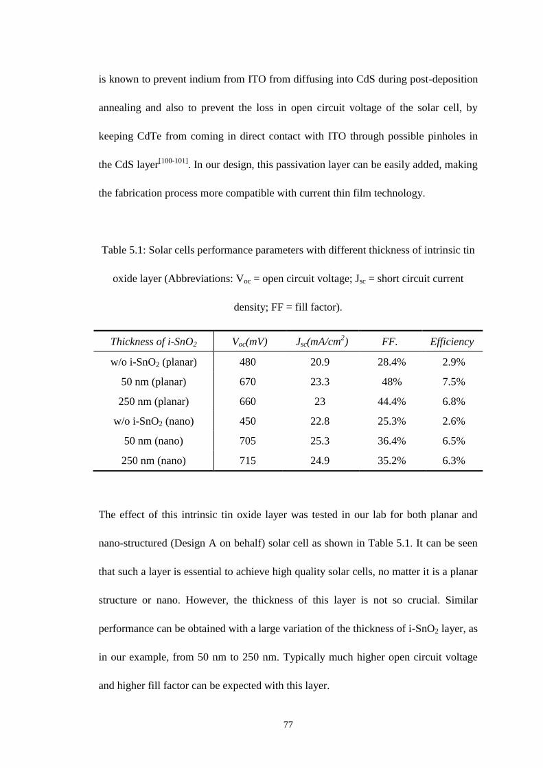
77
is known to prevent indium from ITO from diffusing into CdS during post-deposition
annealing and also to prevent the loss in open circuit voltage of the solar cell, by
keeping CdTe from coming in direct contact with ITO through possible pinholes in
the CdS layer[100-101]
. In our design, this passivation layer can be easily added, making
the fabrication process more compatible with current thin film technology.
Table 5.1: Solar cells performance parameters with different thickness of intrinsic tin
oxide layer (Abbreviations: Voc = open circuit voltage; Jsc = short circuit current
density; FF = fill factor).
Thickness of i-SnO2 Voc(mV) Jsc(mA/cm2) FF. Efficiency
w/o i-SnO2 (planar) 480 20.9 28.4% 2.9%
50 nm (planar) 670 23.3 48% 7.5%
250 nm (planar) 660 23 44.4% 6.8%
w/o i-SnO2 (nano) 450 22.8 25.3% 2.6%
50 nm (nano) 705 25.3 36.4% 6.5%
250 nm (nano) 715 24.9 35.2% 6.3%
The effect of this intrinsic tin oxide layer was tested in our lab for both planar and
nano-structured (Design A on behalf) solar cell as shown in Table 5.1. It can be seen
that such a layer is essential to achieve high quality solar cells, no matter it is a planar
structure or nano. However, the thickness of this layer is not so crucial. Similar
performance can be obtained with a large variation of the thickness of i-SnO2 layer, as
in our example, from 50 nm to 250 nm. Typically much higher open circuit voltage
and higher fill factor can be expected with this layer.

78
5.2 Fabrication process of CdS NW – CdTe solar cell
5.2.1 Fabrication of ordered AAO template on i-SnO2/ITO/Glass substrate
Commercially available ITO (150~200 nm thick) on glass (~1mm thick) substrates
were cut into 1”x1” pieces and cleaned in acetone and methanol, followed by
de-ionized water rinse and nitrogen blow dry. Then these substrates were subjected to
a 4 minutes plasma etch in oxygen to remove all the organic residues. An intrinsic tin
oxide layer was deposited on ITO by either direct sputtering of SnO2 target or thermal
evaporation of tin metal followed by annealing in oxygen at 550°C for half an hour.
As a process detail, special attention is required to ascertain that this i-SnO2 layer as
well as the underlying ITO layer is smooth and flat so that no distortion of nano pores
will occur during the subsequent anodization step; for reference, distorted AAO on
curved SnO2 surface is shown in Figure 5.3[98]
. Note, further, that in the device
configuration described here, the ITO/i-SnO2 layer combination can be easily
replaced by other materials such as Cd2SnO4/ZnSnO4 combination for future
improvements in device performance[102]
.
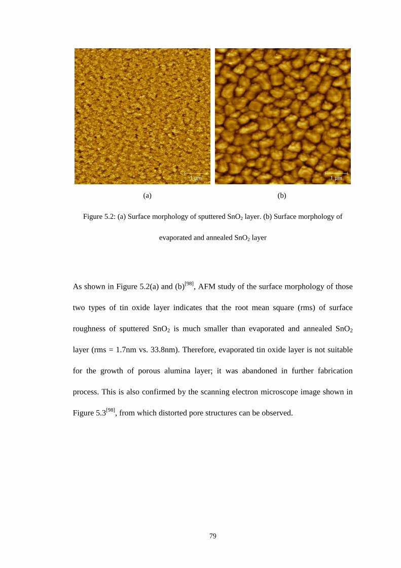
79
(a) (b)
Figure 5.2: (a) Surface morphology of sputtered SnO2 layer. (b) Surface morphology of
evaporated and annealed SnO2 layer
As shown in Figure 5.2(a) and (b)[98]
, AFM study of the surface morphology of those
two types of tin oxide layer indicates that the root mean square (rms) of surface
roughness of sputtered SnO2 is much smaller than evaporated and annealed SnO2
layer (rms = 1.7nm vs. 33.8nm). Therefore, evaporated tin oxide layer is not suitable
for the growth of porous alumina layer; it was abandoned in further fabrication
process. This is also confirmed by the scanning electron microscope image shown in
Figure 5.3[98]
, from which distorted pore structures can be observed.

80
Figure 5.3: Distorted AAO templates on top of thermal evaporated and annealed SnO2 layer
In contrast, AAO template grown on sputtered SnO2 showed straight and ordered pore
structures, as seen in Figure 5.4[98]
.
Figure 5.4: Ordered porous alumina templates on top of sputtered SnO2 layer on ITO/Glass
for building front-wall structured nanowire CdS/CdTe based solar cells

81
To make AAO templates on top of ITO/SnO2, a thin layer of aluminum metal was
deposited by electron beam evaporation and anodized at a potential of 50 V in a 0.3M
oxalic acid solution. Pores of 60 nm diameter and 100-300 nm thickness in a matrix of
aluminum oxide were thus obtained. Note that the thickness of intrinsic SnO2 layer as
well as the AAO layer can be tailored as needed for comparison purpose. An example
with 250 nm of SnO2 and 400 nm of AAO is shown in Figure 5.5.
Figure 5.5: 400 nm AAO template on 250 nm i-SnO2 layer on ITO/Glass
5.2.2 Fabrication and characterization of CdS NW
The electrolyte for CdS deposition was composed of 0.055M CdCl2 and 0.19M
elemental sulfur, dissolved in 50 mL dimethyl sulfoxide (DMSO) and heated up to

82
120°C. Under dc electrodeposition condition, a constant current density of 7.5mA/cm2
was applied for 7 ~ 13 seconds. The estimated growth rate was ~30 nm per second.
Thus, CdS nanowires of controlled length were deposited into these templates by
direct-current electrodeposition[86]
.
The samples were then dipped in saturated CdCl2 in methanol solution and annealed
in argon gas at 400°C for 10 minutes. This step was to facilitate the recrystalization
and purification of CdS nanowires and condition the surface prior to CdTe
deposition[103]
. Other types of treatment have also been tried for comparison, such as
annealing in hydrogen or air. However, none of them showed good performance in
probe voltage test as shown in Table 5.2, thus were not chosen for future
consideration (usually only cells with probe voltage larger than 600 mV are chosen
for further proceeding).
Table 5.2: Probe voltage tests of CdS-CdTe solar cells with different conditions of
treatment after CdS deposition.
Conditions of treatment Probe voltage (mV)
Pure hydrogen, 400°C for 10 minutes 400
Pure oxygen, 400°C for 10 minutes 280
Air, 400°C for 10 minutes 510
CdCl2 dip & anneal in Ar, 400°C for 10 minutes 700
Dilute HCl dip & anneal in Ar, 400°C for 10 minutes 530
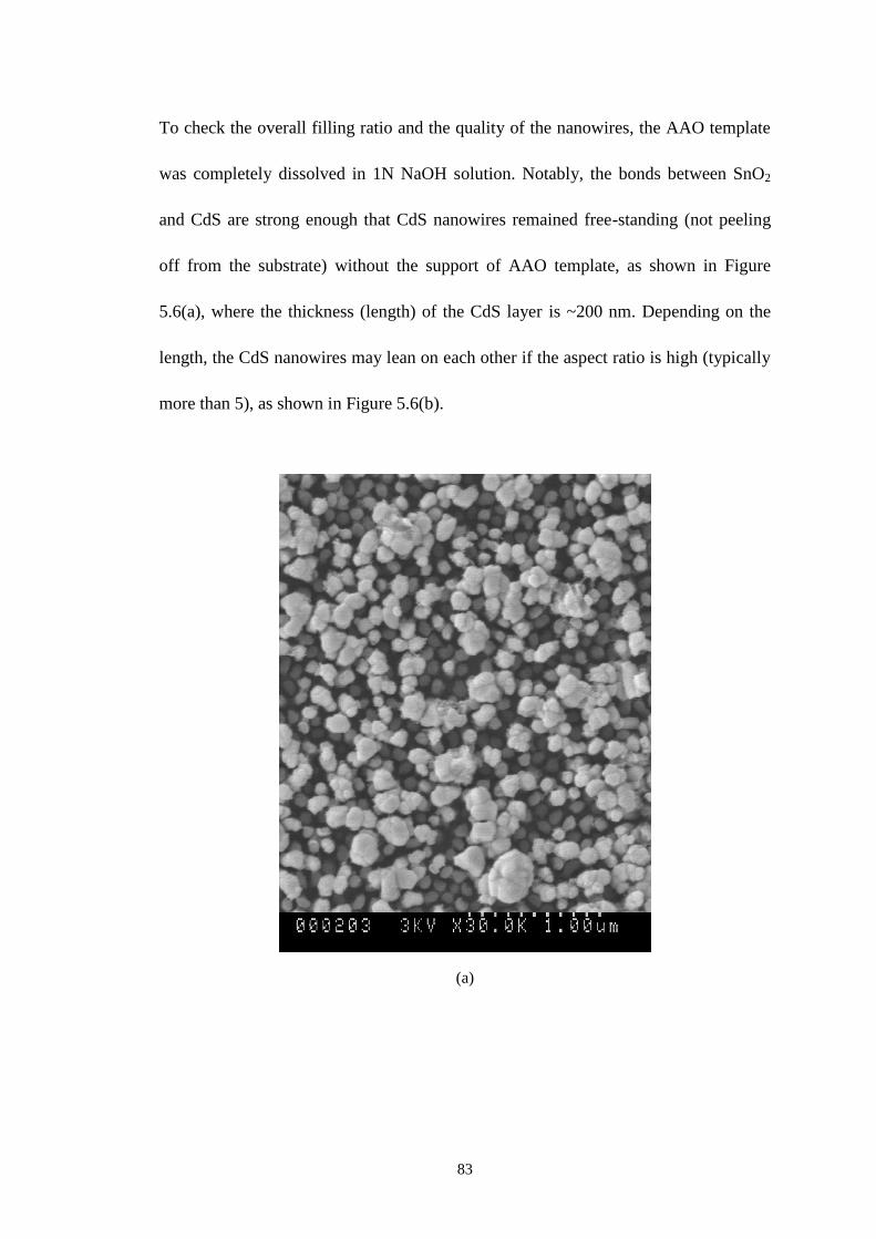
83
To check the overall filling ratio and the quality of the nanowires, the AAO template
was completely dissolved in 1N NaOH solution. Notably, the bonds between SnO2
and CdS are strong enough that CdS nanowires remained free-standing (not peeling
off from the substrate) without the support of AAO template, as shown in Figure
5.6(a), where the thickness (length) of the CdS layer is ~200 nm. Depending on the
length, the CdS nanowires may lean on each other if the aspect ratio is high (typically
more than 5), as shown in Figure 5.6(b).
(a)
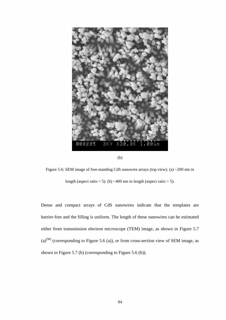
84
(b)
Figure 5.6: SEM image of free-standing CdS nanowire arrays (top view). (a) ~200 nm in
length (aspect ratio < 5). (b) ~400 nm in length (aspect ratio > 5).
Dense and compact arrays of CdS nanowires indicate that the templates are
barrier-free and the filling is uniform. The length of these nanowires can be estimated
either from transmission electron microscope (TEM) image, as shown in Figure 5.7
(a)[98]
(corresponding to Figure 5.6 (a)), or from cross-section view of SEM image, as
shown in Figure 5.7 (b) (corresponding to Figure 5.6 (b)).

85
(a)
(b)
Figure 5.7: (a) TEM image of released CdS nanowires. (b) SEM image of free-standing CdS
nanowires on i-SnO2/ITO/Glass substrate (cross-section view).
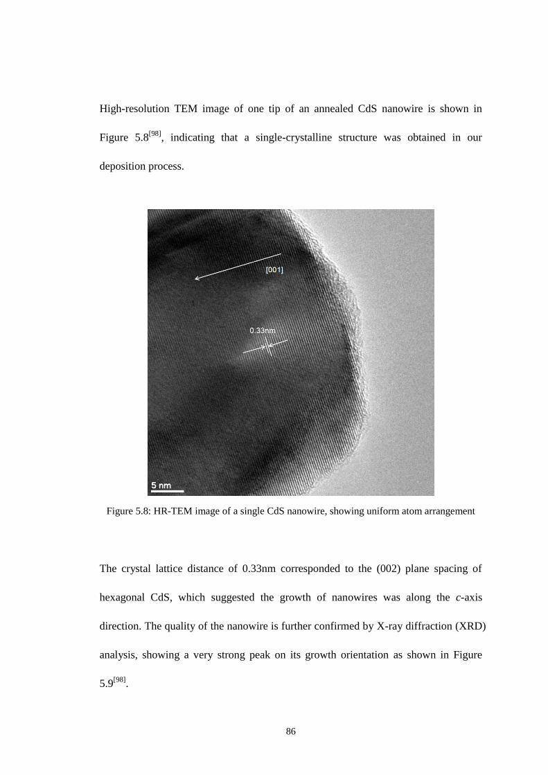
86
High-resolution TEM image of one tip of an annealed CdS nanowire is shown in
Figure 5.8[98]
, indicating that a single-crystalline structure was obtained in our
deposition process.
Figure 5.8: HR-TEM image of a single CdS nanowire, showing uniform atom arrangement
The crystal lattice distance of 0.33nm corresponded to the (002) plane spacing of
hexagonal CdS, which suggested the growth of nanowires was along the c-axis
direction. The quality of the nanowire is further confirmed by X-ray diffraction (XRD)
analysis, showing a very strong peak on its growth orientation as shown in Figure
5.9[98]
.
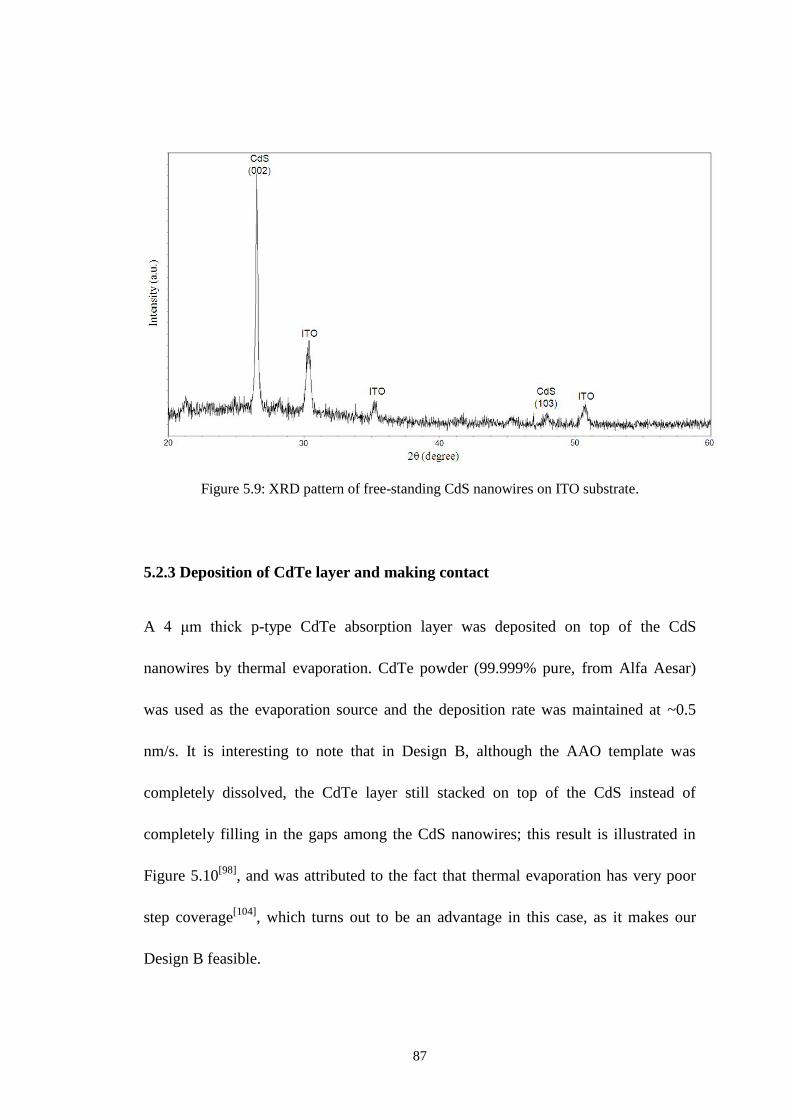
87
Figure 5.9: XRD pattern of free-standing CdS nanowires on ITO substrate.
5.2.3 Deposition of CdTe layer and making contact
A 4 μm thick p-type CdTe absorption layer was deposited on top of the CdS
nanowires by thermal evaporation. CdTe powder (99.999% pure, from Alfa Aesar)
was used as the evaporation source and the deposition rate was maintained at ~0.5
nm/s. It is interesting to note that in Design B, although the AAO template was
completely dissolved, the CdTe layer still stacked on top of the CdS instead of
completely filling in the gaps among the CdS nanowires; this result is illustrated in
Figure 5.10[98]
, and was attributed to the fact that thermal evaporation has very poor
step coverage[104]
, which turns out to be an advantage in this case, as it makes our
Design B feasible.
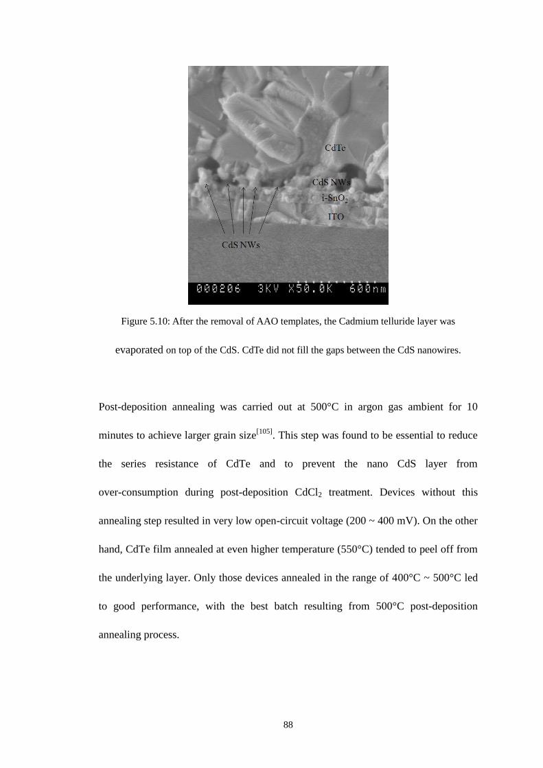
88
Figure 5.10: After the removal of AAO templates, the Cadmium telluride layer was
evaporated on top of the CdS. CdTe did not fill the gaps between the CdS nanowires.
Post-deposition annealing was carried out at 500°C in argon gas ambient for 10
minutes to achieve larger grain size[105]
. This step was found to be essential to reduce
the series resistance of CdTe and to prevent the nano CdS layer from
over-consumption during post-deposition CdCl2 treatment. Devices without this
annealing step resulted in very low open-circuit voltage (200 ~ 400 mV). On the other
hand, CdTe film annealed at even higher temperature (550°C) tended to peel off from
the underlying layer. Only those devices annealed in the range of 400°C ~ 500°C led
to good performance, with the best batch resulting from 500°C post-deposition
annealing process.
89
The devices were then dipped in saturated CdCl2 solution and annealed in argon gas at
387°C for 15 minutes, to purify the crystallites and to reduce the interface states
density[106]
.
Before putting contacts, the samples were etched in a mixture of nitric and phosphoric
acid (1% HNO3, 70% H3PO4, 29% H2O) for 30 seconds to clean the surface and form
a tellurium-rich (Te+) layer
[107]. Then, a 3 nm thick copper layer was deposited onto
the tellurium-rich surface by sputtering, followed by the application of graphite paste
electrode[108]
. Next, the samples were heated at 200°C for 10 minutes to form a Cu2Te
layer as well as to cure the graphite paste. Last, silver paste was painted uniformly on
the graphite paste to form the top contact and on the ITO layer to form the bottom
contact. The samples were heated again at 200°C for 10 minutes to cure the silver
paste layer. It is interesting to note, again, that the Design B structure was able to
withstand all these post-deposition thermal and etching treatments without the
collapse of the CdS nanopillars.
Current-voltage (I-V) characteristics were measured automatically by a LabView
program, controlling power supply and two digital multimeters for voltage and current
measurement respectively. The illumination intensity was kept at ~100mW/cm2 at
sample surface and light entered from the CdS side.
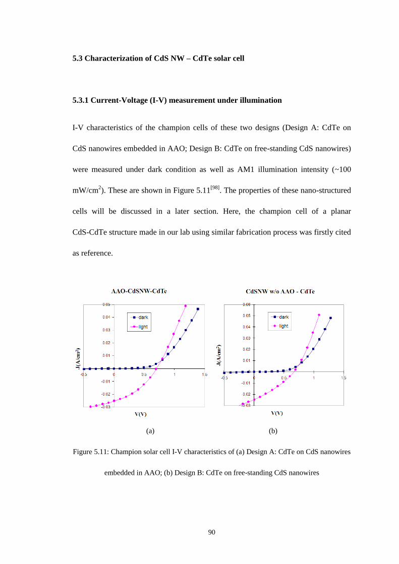
90
5.3 Characterization of CdS NW – CdTe solar cell
5.3.1 Current-Voltage (I-V) measurement under illumination
I-V characteristics of the champion cells of these two designs (Design A: CdTe on
CdS nanowires embedded in AAO; Design B: CdTe on free-standing CdS nanowires)
were measured under dark condition as well as AM1 illumination intensity (~100
mW/cm2). These are shown in Figure 5.11
[98]. The properties of these nano-structured
cells will be discussed in a later section. Here, the champion cell of a planar
CdS-CdTe structure made in our lab using similar fabrication process was firstly cited
as reference.
(a) (b)
Figure 5.11: Champion solar cell I-V characteristics of (a) Design A: CdTe on CdS nanowires
embedded in AAO; (b) Design B: CdTe on free-standing CdS nanowires
91
5.3.2 I-V characteristic of the champion planar cell
Note that in this best planar solar cell, the CdS layer was made by chemical bath
deposition (CBD) instead of electrodeposition (ED). We tried to use the same process
to prepare both planar and nano CdS for a better controlled comparison. However, it
turned out that an electrodeposited planar CdS film did not stick well on the substrate
during post-deposition annealing. After evaporation of CdTe, the planar CdS peeled
off from the under-layer during high temperature treatment.
On the other hand, we also tried to produce CdS nanowires by chemical bath
deposition. However, it formed nano dots along the walls of AAO instead of forming
a continuous wire. Thus, we chose to prepare the planar CdS film by CBD and
prepare the CdS NW by ED. Nevertheless, the champion planar CdS-CdTe solar cell
in the world was made by CBD, as far as we know. Except for this layer, all other
processes were maintained the same for both planar and nano structured devices.
The I-V characteristic of the champion planar cell is shown in Figure 5.12.
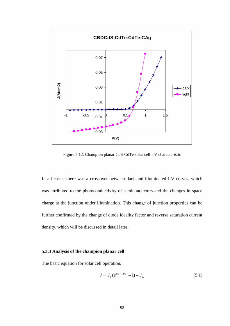
92
CBDCdS-CdTe-CdTe-CAg
-0.03
-0.01
0.01
0.03
0.05
0.07
-1 -0.5 0 0.5 1 1.5
V(V)
J(A
/cm
2)
dark
light
Figure 5.12: Champion planar CdS-CdTe solar cell I-V characteristic
In all cases, there was a crossover between dark and illuminated I-V curves, which
was attributed to the photoconductivity of semiconductors and the changes in space
charge at the junction under illumination. This change of junction properties can be
further confirmed by the change of diode ideality factor and reverse saturation current
density, which will be discussed in detail later.
5.3.3 Analysis of the champion planar cell
The basic equation for solar cell operation,
L
AkTqV JeJJ )1(0 (5.1)
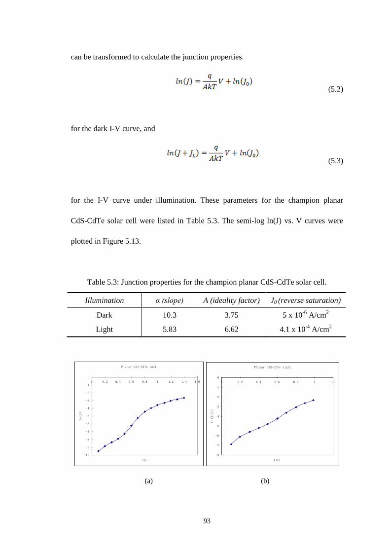
93
can be transformed to calculate the junction properties.
(5.2)
for the dark I-V curve, and
(5.3)
for the I-V curve under illumination. These parameters for the champion planar
CdS-CdTe solar cell were listed in Table 5.3. The semi-log ln(J) vs. V curves were
plotted in Figure 5.13.
Table 5.3: Junction properties for the champion planar CdS-CdTe solar cell.
Illumination α (slope) A (ideality factor) J0 (reverse saturation)
Dark 10.3 3.75 5 x 10⁻⁶
A/cm2
Light 5.83 6.62 4.1 x 10⁻⁴
A/cm2
Planar CdS-CdTe dark
-10
-9
-8
-7
-6
-5
-4
-3
-2
-1
0
0 0.2 0.4 0.6 0.8 1 1.2 1.4 1.6
(V)
ln(J)
Planar CdS-CdTe light
-8
-7
-6
-5
-4
-3
-2
-1
0
0 0.2 0.4 0.6 0.8 1 1.2
V(V)
ln(J+JL)
(a) (b)
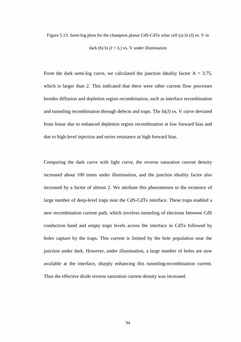
94
Figure 5.13: Semi-log plots for the champion planar CdS-CdTe solar cell (a) ln (J) vs. V in
dark (b) ln (J + JL) vs. V under illumination
From the dark semi-log curve, we calculated the junction ideality factor A = 3.75,
which is larger than 2. This indicated that there were other current flow processes
besides diffusion and depletion region recombination, such as interface recombination
and tunneling recombination through defects and traps. The ln(J) vs. V curve deviated
from linear due to enhanced depletion region recombination at low forward bias and
due to high-level injection and series resistance at high forward bias.
Comparing the dark curve with light curve, the reverse saturation current density
increased about 100 times under illumination, and the junction ideality factor also
increased by a factor of almost 2. We attribute this phenomenon to the existence of
large number of deep-level traps near the CdS-CdTe interface. These traps enabled a
new recombination current path, which involves tunneling of electrons between CdS
conduction band and empty traps levels across the interface in CdTe followed by
holes capture by the traps. This current is limited by the hole population near the
junction under dark. However, under illumination, a large number of holes are now
available at the interface, sharply enhancing this tunneling-recombination current.
Thus the effective diode reverse saturation current density was increased.
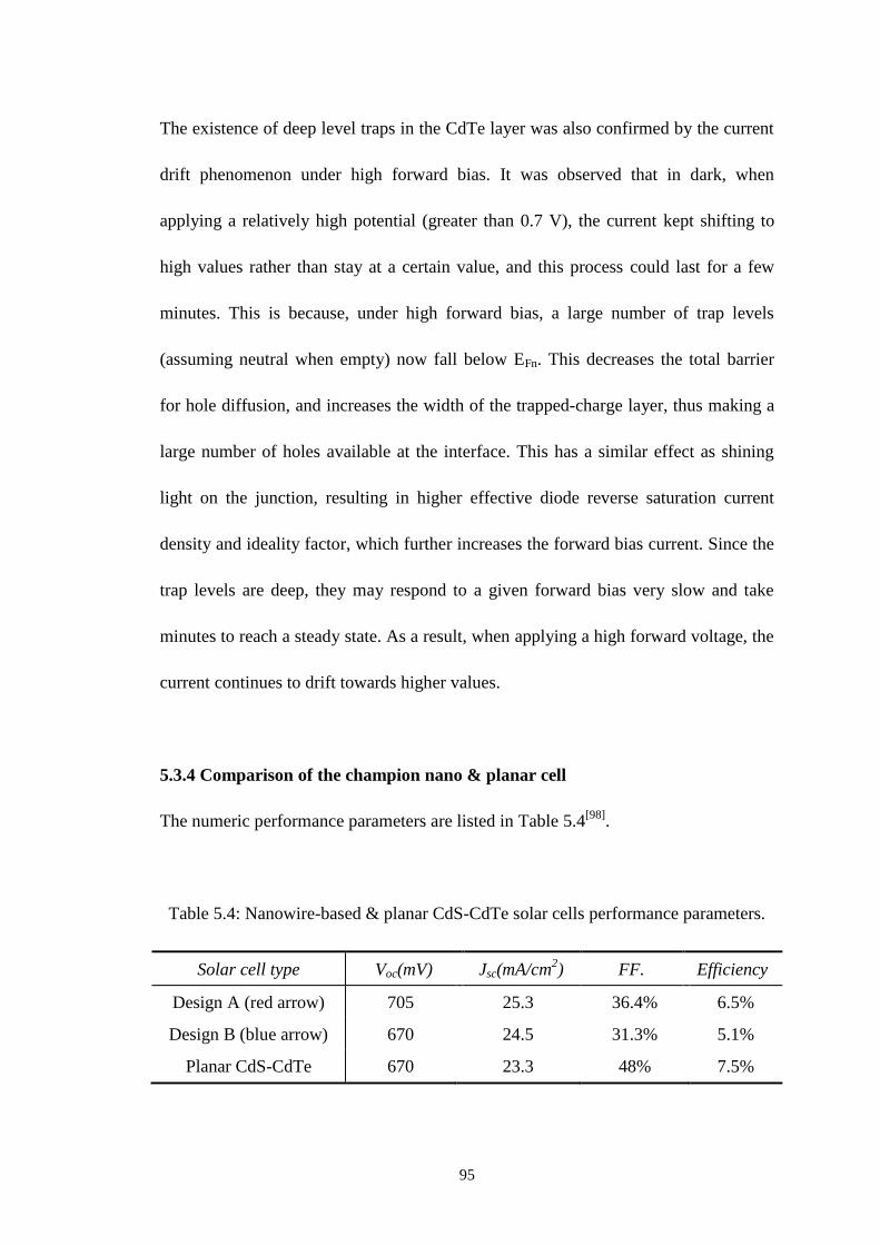
95
The existence of deep level traps in the CdTe layer was also confirmed by the current
drift phenomenon under high forward bias. It was observed that in dark, when
applying a relatively high potential (greater than 0.7 V), the current kept shifting to
high values rather than stay at a certain value, and this process could last for a few
minutes. This is because, under high forward bias, a large number of trap levels
(assuming neutral when empty) now fall below EFn. This decreases the total barrier
for hole diffusion, and increases the width of the trapped-charge layer, thus making a
large number of holes available at the interface. This has a similar effect as shining
light on the junction, resulting in higher effective diode reverse saturation current
density and ideality factor, which further increases the forward bias current. Since the
trap levels are deep, they may respond to a given forward bias very slow and take
minutes to reach a steady state. As a result, when applying a high forward voltage, the
current continues to drift towards higher values.
5.3.4 Comparison of the champion nano & planar cell
The numeric performance parameters are listed in Table 5.4[98]
.
Table 5.4: Nanowire-based & planar CdS-CdTe solar cells performance parameters.
Solar cell type Voc(mV) Jsc(mA/cm2) FF. Efficiency
Design A (red arrow) 705 25.3 36.4% 6.5%
Design B (blue arrow) 670 24.5 31.3% 5.1%
Planar CdS-CdTe 670 23.3 48% 7.5%

96
Note that more than five samples of each type were made, but only the best cells are
compared here, because the average value of each performance parameter of all these
samples follows the same trend as the best samples. From the upper part of Table 5.4
(comparing nano design A & B), we can see that the solar cell with embedded CdS
nanowires has higher values of open circuit voltage, fill factor, short circuit current
density and power conversion efficiency. In comparison with Design B, the nanowires
in Design A are better isolated from the outer ambient. Another advantage of Design
A is that it contains less shunting paths. Even in very high quality planar CdS thin
films, pinholes cannot be completely avoided and some CdTe tentacles can come in
direct contact with the SnO2 under layer, resulting in shunting paths. The same thing
will happen in Design B. On the contrary, in Design A, even if pinholes form in the
CdS layer during electrodeposition, approximately half the area remains covered with
aluminum oxide, which prevents CdTe layer from touching the electrode layer. As a
result, the shunt resistance of Design A is higher than that of Design B. In addition,
the AAO matrix among the CdS nanowires makes the film more stable than in the
case of gaps among nanowires; this makes Design A more robust.
Comparing the nano cells with planar CdS-CdTe, the nano-structured solar cells
typically have higher or similar open circuit voltage, higher short circuit current, as
was expected (see Chapter 3 – simulation for details). However, they showed lower
overall conversion efficiency due to much lower fill factor, which was the combined
97
effect of series resistance and shunt resistance. These values were estimated from the
I-V curves and listed in Table 5.5 for reference.
Table 5.5: Series & shunt resistances of NW & planar CdS-CdTe solar cells.
Solar cell type Rs (series resistance) Rsh (shunt resistance)
Design A (embedded in AAO) 9 Ω∙cm2 130 Ω∙cm
2
Design B (free-standing) 6.8 Ω∙cm2 45 Ω∙cm
2
Planar CdS-CdTe 3.7 Ω∙cm2 140 Ω∙cm
2
From Table 5.5, we can see that nano Design A has similar shunt resistance as the
planar cell, but much higher series resistance. This could be resulted from the extra
distance that a photo-generated electron in the CdTe on top of the aluminum oxide
instead of CdS needs to travel to reach the CdS nanowire. On the other hand,
considering the effects of process variation, there could be a small portion of CdS
NWs that didn‟t reach the top surface of AAO, resulting in a gap between the tips of
CdS NWs and the top CdTe film. The photo-generated electrons in the CdTe on top of
these gaps will need to travel another extra distance to reach the nearest CdS nanowire,
further increasing the series resistance of this device. For similar reasons, the series
resistance of nano Design B is higher than planar device, but lower than Design A
because after the removal of AAO template, even those shorter CdS NWs could get in
touch with the top CdTe layer.
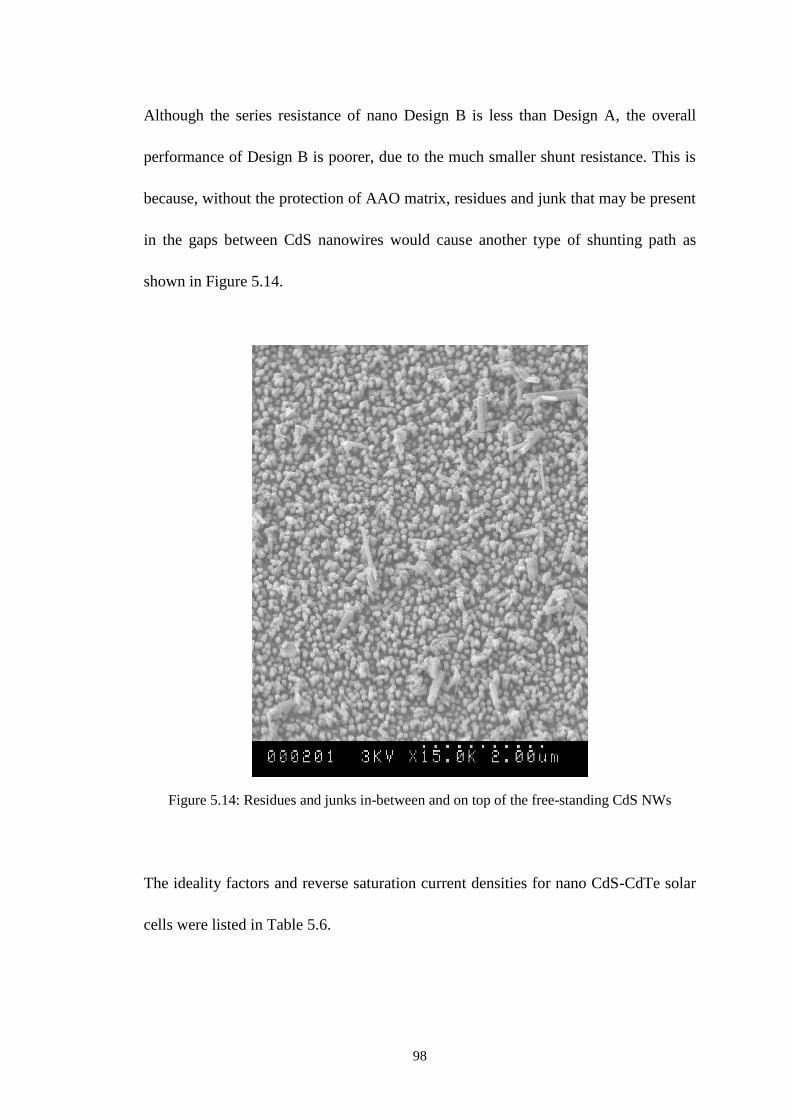
98
Although the series resistance of nano Design B is less than Design A, the overall
performance of Design B is poorer, due to the much smaller shunt resistance. This is
because, without the protection of AAO matrix, residues and junk that may be present
in the gaps between CdS nanowires would cause another type of shunting path as
shown in Figure 5.14.
Figure 5.14: Residues and junks in-between and on top of the free-standing CdS NWs
The ideality factors and reverse saturation current densities for nano CdS-CdTe solar
cells were listed in Table 5.6.
99
Table 5.6: Junction properties for the champion nano CdS-CdTe solar cells of both
device configurations.
Illumination α (slope) A (ideality factor) J0 (reverse saturation)
Dark (Design A) 8.2 4.7 1.7 x 10⁻⁵
A/cm2
Light (Design A) 3.5 11 1.8 x 10⁻³
A/cm2
Dark (Design B) 7.4 5.3 2.8 x 10⁻⁵
A/cm2
Light (Design B) 3 12.7 3 x 10⁻³
A/cm2
Here we noticed a similar relationship between the dark properties and light properties
of a nano device as compared with a planar device. In both cases, the reverse bias
saturation current density increased about 100 times under illumination, and the
junction ideality factor also increased by a factor of 2 ~ 3. And this is also true for
both designs of nano-structured solar cells. This fact further confirmed a large number
of deep-level traps in the CdTe layer near the CdS-CdTe interface because in all three
devices, the CdTe bulk layer was deposited and treated the same way. Thus, despite
the differences in the CdS layer structure design, the increments of reverse saturation
current density and ideality factor were about the same.
On the other hand, the nano devices have larger values of reverse bias saturation
current densities and ideality factors than the planar device. This is in contradiction
with what we expected when we performed simulation. However, in our simulation,
we assumed that the junction quality and carrier transportation mechanism were the
same for both planar and nano devices. As a matter of fact, it is not the case. It could
be attributed to the different surface conditions resulted from different methods of

100
CdS deposition. In conclusion, the nano-structured CdS-CdTe solar cell devices have
poorer performance than simulated results because of their lower junction quality at
the nano-CdS/CdTe interface.
5.3.5 Effects of CdS NW length on the device performance
To study the influence of nanowire length on the performance of solar cells, the AAO
template thicknesses were varied from 100 nm to 300 nm (in Design A) or from 200
nm to 400 nm (in Design B) and filled with CdS nanowires with lengths ranging from
100 nm to 300 nm (equal to the template thickness in Design A or 100 nm less than
the template thickness in Design B). They were all fabricated under the same process
conditions except the deposition time of CdS. Performance parameters of these solar
cells are shown in Figure 5.15[98]
.
(a) (b)
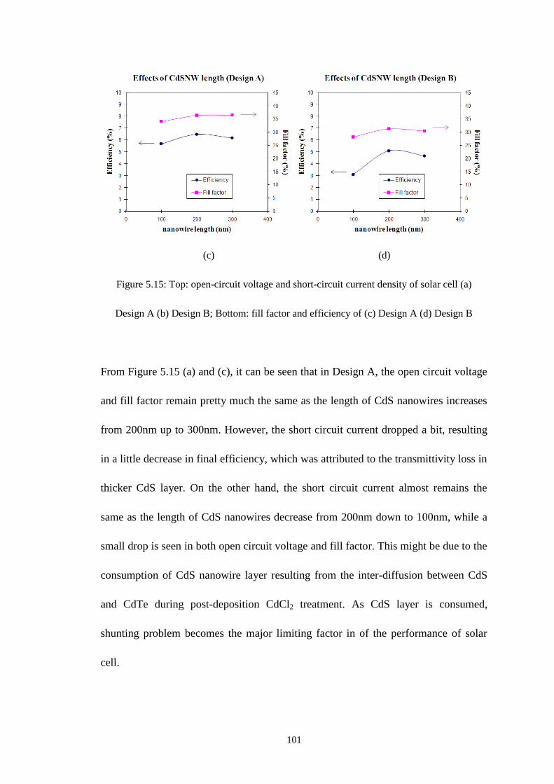
101
(c) (d)
Figure 5.15: Top: open-circuit voltage and short-circuit current density of solar cell (a)
Design A (b) Design B; Bottom: fill factor and efficiency of (c) Design A (d) Design B
From Figure 5.15 (a) and (c), it can be seen that in Design A, the open circuit voltage
and fill factor remain pretty much the same as the length of CdS nanowires increases
from 200nm up to 300nm. However, the short circuit current dropped a bit, resulting
in a little decrease in final efficiency, which was attributed to the transmittivity loss in
thicker CdS layer. On the other hand, the short circuit current almost remains the
same as the length of CdS nanowires decrease from 200nm down to 100nm, while a
small drop is seen in both open circuit voltage and fill factor. This might be due to the
consumption of CdS nanowire layer resulting from the inter-diffusion between CdS
and CdTe during post-deposition CdCl2 treatment. As CdS layer is consumed,
shunting problem becomes the major limiting factor in of the performance of solar
cell.
102
This phenomenon is more obvious in the case of Design B, as we can see from Figure
5.15 (b) & (d). Severe drop of open circuit voltage, short circuit current and fill factor
occurred when the length of CdS nanowires was decreased to 100 nm, resulting in a
large loss in efficiency. Clearly, a device of Design B can be expected to be more
vulnerable to unintended process variations than a device of Design A. Meanwhile,
the slight drop in the efficiency of 300 nm sample of Design B was attributed to the
same reason as for the device of Design A.
For cells without the protection of AAO matrix, residues and junk that may be present
in the gaps between CdS nanowires would cause another type of shunting path,
accounting for the average lower efficiency of Design B solar cells. Unlike the case of
the hybrid 3D junction structure of Javey group, where both lateral and vertical
junctions are present and efficiency values increase greatly as the lengths of CdS
nanowires increases, in our structure, not much change occurred with the change of
CdS nanowire length, as there was no essential change in the junction. Instead, it was
the change of CdS transmittivity that played the dominant role in efficiency
enhancement. Nevertheless, in the case of short nanowires, there can be some changes
in the junction quality as the consumption of CdS layer becomes severe.

103
5.3.6 Capacitance-Voltage (C-V) measurement of CdS NW – CdTe solar cell
To further understand the characteristics of the nano-structured CdS-CdTe solar cell,
the capacitance of the champion cell was measured as a function of applied bias at
different frequencies. The results were shown in Figure 5.16.
C-V @ 5KHz
0.00E+00
5.00E-10
1.00E-09
1.50E-09
2.00E-09
2.50E-09
3.00E-09
3.50E-09
4.00E-09
4.50E-09
-1.5 -1 -0.5 0 0.5 1 1.5 2
V(V)
C(F
)
(a)
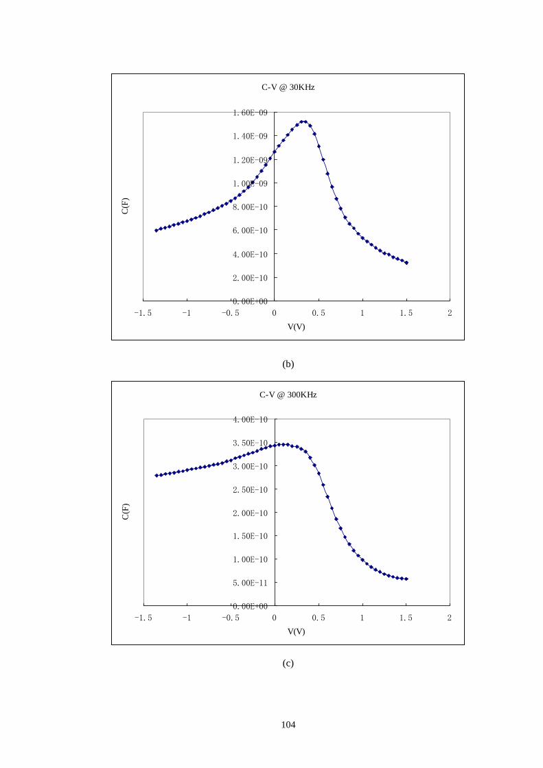
104
C-V @ 30KHz
0.00E+00
2.00E-10
4.00E-10
6.00E-10
8.00E-10
1.00E-09
1.20E-09
1.40E-09
1.60E-09
-1.5 -1 -0.5 0 0.5 1 1.5 2
V(V)
C(F
)
(b)
C-V @ 300KHz
0.00E+00
5.00E-11
1.00E-10
1.50E-10
2.00E-10
2.50E-10
3.00E-10
3.50E-10
4.00E-10
-1.5 -1 -0.5 0 0.5 1 1.5 2
V(V)
C(F
)
(c)
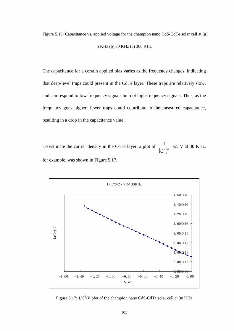
105
Figure 5.16: Capacitance vs. applied voltage for the champion nano CdS-CdTe solar cell at (a)
5 KHz (b) 30 KHz (c) 300 KHz
The capacitance for a certain applied bias varies as the frequency changes, indicating
that deep-level traps could present in the CdTe layer. These traps are relatively slow,
and can respond to low-frequency signals but not high-frequency signals. Thus, as the
frequency goes higher, fewer traps could contribute to the measured capacitance,
resulting in a drop in the capacitance value.
To estimate the carrier density in the CdTe layer, a plot of 2*
1
C vs. V at 30 KHz,
for example, was shown in Figure 5.17.
1/(C*)^2 - V @ 30KHz
0.00E+00
2.00E+15
4.00E+15
6.00E+15
8.00E+15
1.00E+16
1.20E+16
1.40E+16
1.60E+16
-1.60 -1.40 -1.20 -1.00 -0.80 -0.60 -0.40 -0.20 0.00
V(V)
1/(
C*
)^2
Figure 5.17: 1/C2-V plot of the champion nano CdS-CdTe solar cell at 30 KHz
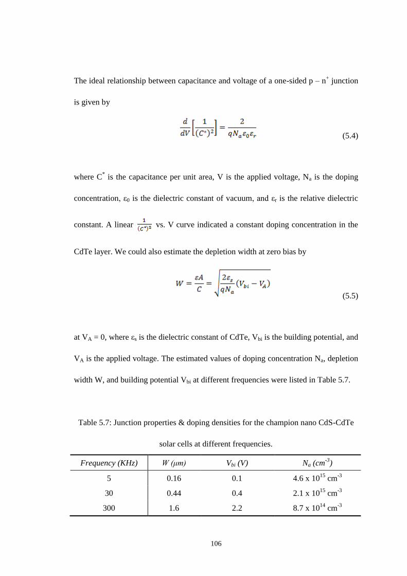
106
The ideal relationship between capacitance and voltage of a one-sided p – n+ junction
is given by
(5.4)
where C* is the capacitance per unit area, V is the applied voltage, Na is the doping
concentration, ε0 is the dielectric constant of vacuum, and εr is the relative dielectric
constant. A linear vs. V curve indicated a constant doping concentration in the
CdTe layer. We could also estimate the depletion width at zero bias by
(5.5)
at VA = 0, where εs is the dielectric constant of CdTe, Vbi is the building potential, and
VA is the applied voltage. The estimated values of doping concentration Na, depletion
width W, and building potential Vbi at different frequencies were listed in Table 5.7.
Table 5.7: Junction properties & doping densities for the champion nano CdS-CdTe
solar cells at different frequencies.
Frequency (KHz) W (μm) Vbi (V) Na (cm-3
)
5 0.16 0.1 4.6 x 10¹⁵
cm-3
30 0.44 0.4 2.1 x 10¹⁵
cm-3
300 1.6 2.2 8.7 x 10¹⁴
cm-3
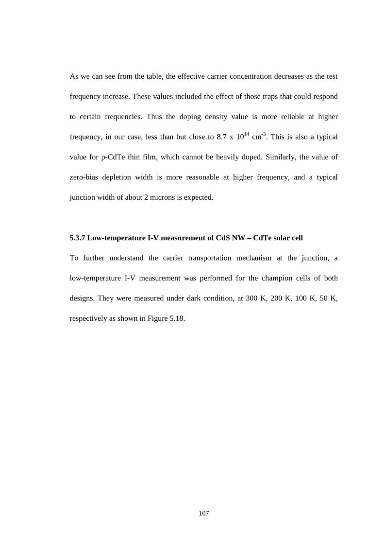
107
As we can see from the table, the effective carrier concentration decreases as the test
frequency increase. These values included the effect of those traps that could respond
to certain frequencies. Thus the doping density value is more reliable at higher
frequency, in our case, less than but close to 8.7 x 10¹⁴
cm-3
. This is also a typical
value for p-CdTe thin film, which cannot be heavily doped. Similarly, the value of
zero-bias depletion width is more reasonable at higher frequency, and a typical
junction width of about 2 microns is expected.
5.3.7 Low-temperature I-V measurement of CdS NW – CdTe solar cell
To further understand the carrier transportation mechanism at the junction, a
low-temperature I-V measurement was performed for the champion cells of both
designs. They were measured under dark condition, at 300 K, 200 K, 100 K, 50 K,
respectively as shown in Figure 5.18.
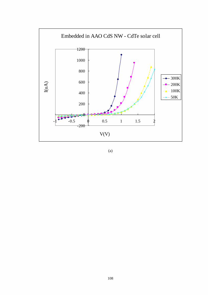
108
Embedded in AAO CdS NW - CdTe solar cell
-200
0
200
400
600
800
1000
1200
-1 -0.5 0 0.5 1 1.5 2
V(V)
I(u
A)
300K
200K
100K
50K
(a)

109
Free-standing CdS NW - CdTe solar cell
-20
-10
0
10
20
30
40
-1.5 -0.5 0.5 1.5
V(V)
I(u
A)
300K
200K
100K
50K
(b)
Figure 5.18: Dark I-V measurement of the champion CdS NW - CdTe solar cells of (a)
Design A, and (b) Design B, at different temperatures
To perform these measurements, samples were mounted at the sample stage on the top
of the cryostat, covered by a metallic shell. A temperature sensor was placed at the
vicinity of the sample to monitor the temperature. The whole system was pumped for
~1 hour to reach low pressure (in the range of 10-1
~ 10-2
Torr) to prevent gas
condensation. A compressor was used to send helium back and forth to continuously
cool down the system, while a heater was used to maintain the sample at a preset
temperature.

110
According to
(5.6)
for a set of I-V curves, we plot their corresponding ln(I) vs. V curves and extract α (α
is the slope of the ln(I) vs. V curve, which equals to ) at different temperatures.
Here, we plot the α vs. 1000/T, as shown in Figure 5.19.
q/AkT vs. 1000/T (Design A)
0
1
2
3
4
5
6
7
8
0 5 10 15 20 25
1000/T (1/K)
q/A
kT
(1
/V)
q/AkT vs. 1000/T (Design B)
0
1
2
3
4
5
6
0 5 10 15 20 25
1000/T (1/K)
q/A
kT
(1
/V)
(a) (b)
Figure 5.19: α ( ) vs. 1000/T plots of the champion CdS NW - CdTe solar cells of (a)
Design A (b) Design B
For an ideal p-n junction where diffusion is the dominating mechanism of charge
transportation, the slope α should be proportional to 1/T. Clearly it is not the case for
our devices. The numbers of α as well as ideality factor A are listed in Table 5.8.
111
Table 5.8: Slope & ideality factors for the champion nano CdS-CdTe solar cells of
both device configurations at different temperatures.
Temperature (K) α (slope) A (ideality factor)
300 (Design A) 7 5.5
200 (Design A) 4.8 12.1
100 (Design A) 3.6 32.2
50 (Design A) 3.6 64.4
300 (Design B) 5.6 7
200 (Design B) 5.3 10.9
100 (Design B) 4.1 28.3
50 (Design B) 4.6 51
From Table 5.8, we can see that the lower the temperature, the farther away the
ideality factor from ideal case of one. This is because, as the temperature (T) goes
lower, the thermal generated carrier diffusion current (the reverse saturation current
density) becomes smaller as indicated by
(5.7)
Thus the recombination current through interface states and deep-level traps becomes
more and more dominant, and the ideality factor deviates further from unity. This
further confirmed that the charge transportation at the junction is the co-effect of
diffusion and defects-assisted recombination, where deep-level traps and interface
states play an important role as indicated by C-V and illumination I-V measurements,
as has been discussed in above sections.
112
5.4 Comments
In summary, we have described novel device configurations for the CdS-CdTe solar
cells where nanowires of CdS, embedded in aluminum oxide, or free standing, are
used as the window semiconductor layer. From theoretical considerations, this leads
to a window layer of higher optical transmission, and a reduced junction area for the
“lossy”, reverse saturation current. As a result, one can expect higher short circuit
current and higher open circuit voltage values, resulting in an estimated 25% increase
in the power conversion efficiency of the CdS-CdTe solar cell as was simulated in
Chapter 3.
Devices of the two nanostructured designs mentioned above were fabricated. In initial
experiments, a power conversion efficiency value of 6.5% for Design A (CdS NW
embedded in AAO) and 5.1% for Design B (free-standing CdS NW) was achieved.
To our knowledge, 6.5% is the highest efficiency among all reported solar cells based
on nanowires, nanodots, nanopillars or nanorods. For this cell, open-circuit voltage,
short-circuit current density and fill factor values were 705mV, 25.3mA/cm2 and
36.4% respectively. Further process optimizations, including reduction of contact
resistance between CdTe and graphite electrode, surface treatment of ITO/SnO2 layers
and replacement of thermal evaporation by close space sublimation for CdTe
deposition, could lead to further enhancement of the conversion efficiency.
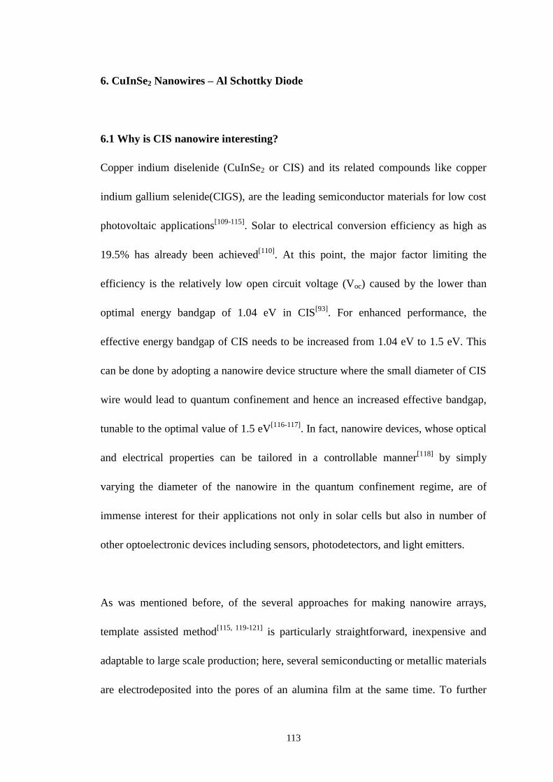
113
6. CuInSe2 Nanowires – Al Schottky Diode
6.1 Why is CIS nanowire interesting?
Copper indium diselenide (CuInSe2 or CIS) and its related compounds like copper
indium gallium selenide(CIGS), are the leading semiconductor materials for low cost
photovoltaic applications[109-115]
. Solar to electrical conversion efficiency as high as
19.5% has already been achieved[110]
. At this point, the major factor limiting the
efficiency is the relatively low open circuit voltage (Voc) caused by the lower than
optimal energy bandgap of 1.04 eV in CIS[93]
. For enhanced performance, the
effective energy bandgap of CIS needs to be increased from 1.04 eV to 1.5 eV. This
can be done by adopting a nanowire device structure where the small diameter of CIS
wire would lead to quantum confinement and hence an increased effective bandgap,
tunable to the optimal value of 1.5 eV[116-117]
. In fact, nanowire devices, whose optical
and electrical properties can be tailored in a controllable manner[118]
by simply
varying the diameter of the nanowire in the quantum confinement regime, are of
immense interest for their applications not only in solar cells but also in number of
other optoelectronic devices including sensors, photodetectors, and light emitters.
As was mentioned before, of the several approaches for making nanowire arrays,
template assisted method[115, 119-121]
is particularly straightforward, inexpensive and
adaptable to large scale production; here, several semiconducting or metallic materials
are electrodeposited into the pores of an alumina film at the same time. To further
114
study the properties of CIS nanowires, a thin layer contact of gold was deposited on
top of the nanowires of CIS to form Al-CIS-Au Schottky diodes. Thus we have laid
the groundwork for characterizing the surface and junction behavior of CIS nanowires
through Schottky analysis. Such a characterization is believed to be essential for the
later development of high efficiency solar cell designs in these nanowires[93]
.
For this first study on the nanowire CIS-Al Schottky diodes, we have used two earlier
studies on this system as benchmarks. One is by Matsushita et al[122]
, who
investigated the CIS-Al Schottky diode on single crystal CIS; the other is by Raffaelle
et al[123]
, who used a polycrystalline film of CIS electrodeposited on molybdenum for
their CIS-Al Schottky diode.
6.2 Fabrication procedure of CIS NW – Al Schottky diode
Device structure of Figure 6.1[93]
showing CIS nanowires inside AAO template on an
aluminum substrate was fabricated by first preparing a short length (~1000 nm)
anodized aluminum oxide template and subsequently filing it with CIS by
electrodeposition.
115
Figure 6.1: Configuration of the device for CIS nanowire - Al Schottky diode measurement
Two-step anodization process was used to prepare the AAO templates. A 60
micrometer thick aluminum sheet with backside protected by glue and paper served as
the anode, and a platinum foil served as the counter electrode[93]
. The electrolyte
contains 0.3M oxalic acid powder dissolved in de-ionized water. The first step
anodization was performed at 20V constant voltage for 10 minutes. The formed
aluminum oxide layer was then etched off in a hot mixture of phosphoric acid and
chromic acid. The second step anodization was performed under a constant potential
of 25V at room temperature for 10 minutes, resulting in a layer of approximately 1
micrometer thick porous alumina.
To remove the thin aluminum oxide barrier layer at the aluminum/porous alumina
interface, we ramped down the anodization voltage at the rate of about 10% per
minutes till it reached a value of 1V. Then the sample was immersed in 50%
phosphoric acid and subjected to a heat treatment in air at 200°C for several hours to

116
convert any possible hydroxide residuals into aluminum oxide. AAO templates with a
typical pore diameter of about 25 nm and pore length of around 1 μm were prepared
by this two-step anodization process.
Next, CuInSe2 nanowires were electrodeposited in the pores by simultaneously
plating all three elements. The bath for CIS nanowire electrodeposition contained 1.5
mM copper sulfate hydrate, 2 mM indium sulfate hydrate and 3.5 mM selenious acid.
The pH was then adjusted to a value of 3 by adding potassium hydrogen phthalate and
hydrochloric acid to the mixture. The electrodeposition was conducted under a dc
pulse voltage of 1 V for 20 minutes at room temperature. Typical current density
during the ED process was 0.25 mA/cm2. For recrysallization, the deposited CIS
nanowires were annealed in Argon gas at 350°C for 1 hour.
These CIS nanowires embedded in the AAO matrix were first characterized by
scanning electron microscope (SEM), energy dispersive X-ray analysis (EDX), and
X-ray diffraction (XRD) to study the material properties. Next, a thin layer of gold
was deposited on top of the nanowires by electron beam evaporation to form ohmic
contact with CIS nanowires. Current-voltage and capacitance-voltage characteristics
of the Al-CIS nanowire Schottky diode, thus obtained, were measured with a
computer controlled set up of a programmable semiconductor parameter analyzer
(Agilent 4155B). Capacitance-voltage measurements were made with a capacitance
meter (Agilent 4284A 20 Hz ~ 1 MHz).

117
6.3 Characterization and analysis of CIS NW – Al Schottky diode
6.3.1 CIS nanowire characteristics
Top view and cross-sectional view of a typical annealed sample of CIS nanowires
inside porous alumina template are shown in Figure 6.2 (a) and (b)[93]
.
(a)

118
(b)
Figure 6.2: SEM images of the CIS nanowires inside porous alumina template: (a) top view (b)
cross-section view
From Figure 6.2, we can see that nanowires grow continuously from the bottom of the
pore, which lies at the aluminum substrate/porous alumina interface, all the way to the
top surface. From the cross-section view, it is estimated that ~90% of the pores are
filled with CIS nanowires and around 80% nanowires are grown all the way through
the pores to the top surface. This is also confirmed by the top view. Note that in the
cross-section view, the AAO template detached from the aluminum substrate, which
119
is attributed to the stress produced during the process of breaking the device and
mounting it on the stub for electron microscopy.
X-ray diffraction measurements on these nanowires showed a pattern corresponding
to a preferential [112] orientation of CIS and a composition close to stoichiometric
CIS was indicated by EDX measurements[115]
.
6.3.2 CIS NW – Al Schottky diode I-V characteristics
By evaporating a thin layer (~100nm) of gold on top of the nanowires to form ohmic
contact to CIS, the Al/CIS(nanowire)/Au Schottky diode device of Figure 6.1 was
obtained. It was used to investigate the electric characteristics of the electrodeposited
CIS nanowires. The current density vs. voltage (J-V) characteristic of an Al/CIS
nanowire Schottky diode is shown in Figure 6.3[93]
; for this measurement, gold
electrode was biased positive with respect to the aluminum electrode.
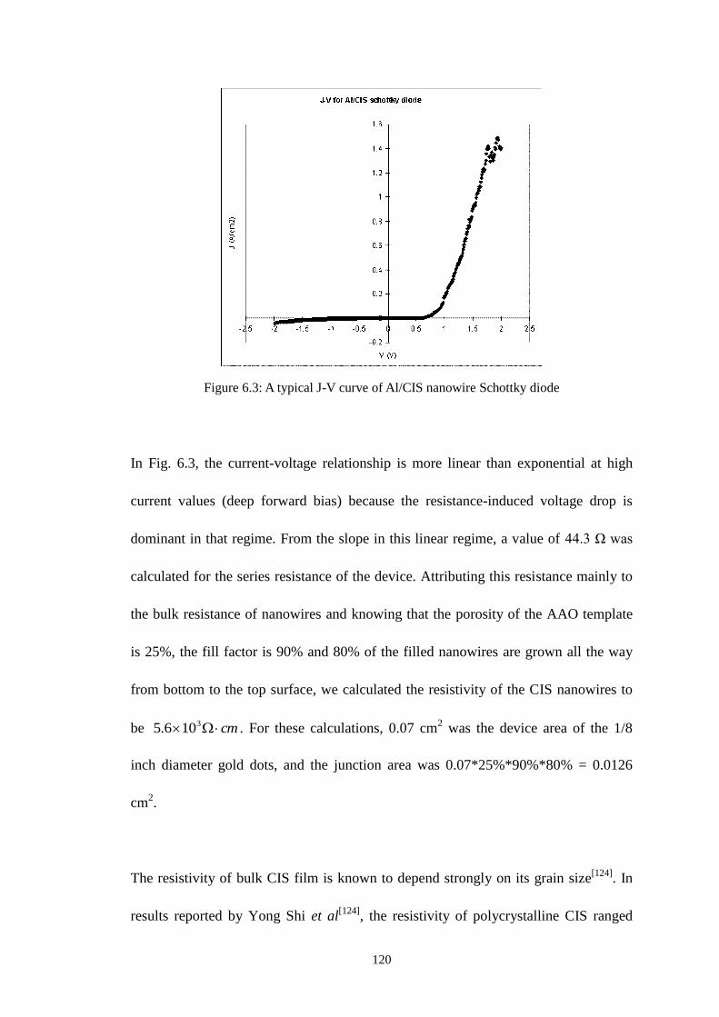
120
Figure 6.3: A typical J-V curve of Al/CIS nanowire Schottky diode
In Fig. 6.3, the current-voltage relationship is more linear than exponential at high
current values (deep forward bias) because the resistance-induced voltage drop is
dominant in that regime. From the slope in this linear regime, a value of 44.3 Ω was
calculated for the series resistance of the device. Attributing this resistance mainly to
the bulk resistance of nanowires and knowing that the porosity of the AAO template
is 25%, the fill factor is 90% and 80% of the filled nanowires are grown all the way
from bottom to the top surface, we calculated the resistivity of the CIS nanowires to
be cm 3106.5 . For these calculations, 0.07 cm2 was the device area of the 1/8
inch diameter gold dots, and the junction area was 0.07*25%*90%*80% = 0.0126
cm2.
The resistivity of bulk CIS film is known to depend strongly on its grain size[124]
. In
results reported by Yong Shi et al[124]
, the resistivity of polycrystalline CIS ranged
121
from 0.58 cm to 516 cm as the grain size decreased from 400 nm to 100 nm
for the same CIS thin film annealed at different temperatures. Resistivity data for CIS
of smaller than 100 nm grain size are not available in the literature because the
as-deposited planar polycrystalline CIS films have grain sizes of around 100 nm and
the grain sizes tend to become even larger as these planar films are subjected to
traditional annealing treatments. The only exception is in our case, where the particle
size is limited by the template pore size and does not increase with annealing
temperature. Thus a resistivity value of cm 3106.5 for a particle size of ~25 nm
is in conformity with the reference[124]
.
It should be noted that, in addition to smaller than 100 nm grain size, other possible
causes for the relatively high resistivity value can include, (i) a thin barrier layer of
aluminum oxide at the Al-CIS interface, (ii) the perturbed nanowire geometry due to
the branched structure of the AAO-CIS at the CIS/Al interface region, and, (iii) the
native oxide layer that forms on top of the CIS nanowire, before the deposition of
gold electrode. It is thought, however, that the barrier layer thickness at the bottom
must have been rather thin because a large number of bubbles were observed at the
end of the phosphoric acid etching process, indicating that the barrier layer had been
at least partially pierced and the underlying aluminum surface exposed to the acid.
Also, further annealing was performed at a relatively low temperature 200ºC. The
native oxide layer on top is also expected to be thin because deposited CIS nanowires
were annealed in argon gas, followed by an immediate evaporation of gold contact.
122
Next, we applied the generalized current density - voltage equation for Schottky diode
1exp0
nkT
qVJJ (6.1)
to analyze the electrical behavior of the semiconductor nanowires. Neglecting the “-1”
term and taking natural logarithm on both sides, we get a linear relationship between
ln(J) and V, and the slope equals nkT
q. Thus we calculated the ideality factor to be n
= 6.4. When compared with the ideality factor values of 3.5 ~ 4.8 reported by Hiroaki
Matsushita et al[122]
for single crystal CIS-Al junction, it is felt that current flow in our
nanowire CIS-Al junctions may be dominated even more by tunneling recombination
through mid-gap traps and interface recombination processes.
Extrapolation of the ln(J) vs. V characteristic yielded the value of the effective reverse
saturation current density to be 5 2
0 9.28 10 /J A cm . This is close to the value
reported by Hiroaki Matsushita et al for the single crystal CIS - Al junctions[122]
.
6.3.3 CIS NW – Al Schottky diode C-V characteristics
Zero bias capacitance measurements on these Schottky diodes revealed that the
capacitance first decreased with frequency (f), at low test frequencies, but became less
and less sensitive as frequency was increased, becoming invariant for f = 1 MHz and
higher. This effect was attributed to a part of the junction space charge being stored in
“slow” mid gap traps in the CIS nanowires. Charge in these traps is able to respond to
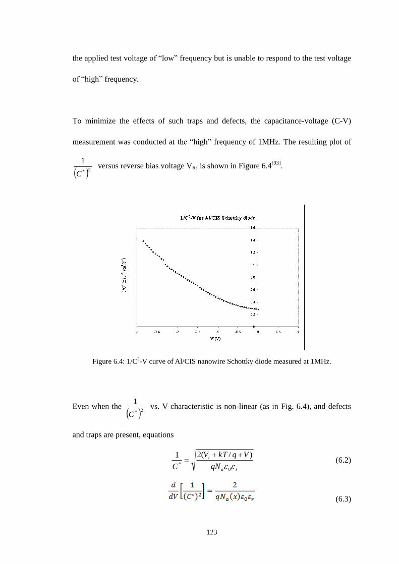
123
the applied test voltage of “low” frequency but is unable to respond to the test voltage
of “high” frequency.
To minimize the effects of such traps and defects, the capacitance-voltage (C-V)
measurement was conducted at the “high” frequency of 1MHz. The resulting plot of
2*
1
C versus reverse bias voltage VR, is shown in Figure 6.4
[93].
Figure 6.4: 1/C2-V curve of Al/CIS nanowire Schottky diode measured at 1MHz.
Even when the 2*
1
C vs. V characteristic is non-linear (as in Fig. 6.4), and defects
and traps are present, equations
sa
i
qN
VqkTV
C 0
*
)/(21 (6.2)
(6.3)
124
where
0sxC
(6.4)
can be used to calculate the variation in local space charge density, qN(x) as a function
of x, where x is the depth inside CIS, from the Al-CIS interface[125]
. N(x) can be thought
of as local “effective carrier concentration”. N(x) is approximately equal to the local
concentration of ionized acceptors, Na(x) in CIS, when the charge stored in local
defects and traps is much smaller than qNa(x). Note that at room temperature, Na(x) is
approximately equal to the local carrier (hole) concentration in CIS.
On the other hand, when charge stored in defects and traps is not much smaller than
qNa(x), then N(x) and Na(x) can differ substantially. N(x) was calculated by using the
above equations and the capacitance-voltage data of Figure 6.4. In this calculation,
junction area of 0.0126 cm2, rather than the device area of 0.07 cm
2 was used. Thus, at
zero bias, the junction capacitance per unit area is 59.5 nF/cm2, which corresponds to
a depletion layer width of 120 nm, where a value of 8.1 is used for the relative
dielectric constant of CIS.
The slope of the plot in Figure 6.4 at zero bias is 1.46 x 10¹⁴
cm4/(F
2∙V), which
corresponds to a value of N = 1.2 x 10¹⁷
cm-3
. In other words, the value of N at the
edge of depletion region, which is 120 nm from the junction with aluminum, is 1.2 x
125
1017
cm-3
. Similarly, the slope of the plot in Figure 6.4 at a bias of -3 V is 7.1 x 10¹⁴
cm4/(F
2∙V), which corresponds to a value of N = 2.45 x 10
16 cm
-3. At this bias, the
junction capacitance value is 26.8 nF/cm2, which corresponds to a depletion layer
width of 267 nm.
For our device, Schottky junction model calculation yielded effective carrier
concentration in the CIS nanowires varying from1.2 x 1017
cm-3
to 2.45 x 10¹⁶
cm-3
as
the distance from the aluminum interface varied from 120 nm to 267 nm. This
variation along the length of nanowire is thought to be related to the differences in the
velocity of ion transport for copper, indium and selenium, down the narrow nanotubes
of porous alumina during electrodeposition. This would lead to changes in the
stoichiometry of CIS as the relative concentration of copper, indium and selenium
changes during the growth of wires in the nanopores, by the electrochemical
deposition process[126]
. Such concentration gradients have been reported earlier in the
electrodeposition of bulk CIS films[127]
.
The composition of the nanowires is more Cu rich at the initial stage of deposition. In
other words, the Cu/In ratio is higher at the interface between aluminum and CIS
nanowires, which results in a higher carrier concentration near the CIS/Al junction. As
the deposition goes on, the Cu component gradually decreases and In composition
gradually increases, and the nanowire composition gradually becomes close to
stochiometric.

126
It should be noted that the composition of bulk electrodeposited CIS films can be
adjusted by post-deposition annealing and recrystallization, making these films
eventually stochiometric. However, in the case of nanowire, post-deposition annealing
seemed to be not as effective. This might be due to the confinement of nanostructure,
which results in less mobility of the atoms during high temperature processes.
Overall, these N values are higher than those (from 315109.5 cm to 315102.2 cm )
reported by Matsushita et al[122]
from C-V measurement at 50 KHz on their single
crystal CIS-Al junctions and the values (from 1.1 x 10¹⁵
cm-3
to 0.28 x 10¹⁵
cm-3
)
reported by Raffaelle et al[123]
on their CIS-Al junctions on polycrystalline films of
CIS electrodeposited on molybdenum substrates.
6.3.4 Band diagram of CIS NW – Al Schottky diode
Equilibrium energy band diagram for the CIS-Al Schottky diode in the ideal case of
zero interface states and traps is shown in Figure 6.5[93]
.

127
Figure 6.5: .Sketch of the energy band diagram of a CIS-Al Schottky diode.
To construct this diagram, the electron affinity values were taken to be 4.48 eV for
CIS[124]
and 4.28 eV for aluminum[59]
; N = 1.2 x 10¹⁷
cm-3
at 120 nm from the CIS/Al
interface and N = 2.45 x 10¹⁶
cm-3
at 267 nm, as obtained from the capacitance
measurements above, and a hole effective mass, mp = 0.71m0 for CIS were used for
calculating EF - EV, from the equations[59]
ln vF V
a
NE E kT
N
(6.5)
32
2
22
p
v
m kTN
h
(6.6)
where, NV is the effective density of states in the valance band of CIS; k is Boltzman‟s
constant; h is Planck‟s constant and T is temperature.
From the energy band diagram sketch of Figure 6.5, the theoretical value of the
built-in junction potential, Vbi is estimated to be 1.12 V. We are not reporting an
128
experimental value of Vbi because, for our device, the extraction of effective junction
barrier height from the capacitance data is complicated by the fact that the 2*
1
C vs.
V plot of Figure 6.4 deviates from linearity and therefore, cannot be extrapolated to
find its intersection with the horizontal voltage axis. In other words, for our device,
the space charge density in CIS is not really known in the first 120 nm distance from
the aluminum interface.
Matsushita et al measured a junction potential of only 0.6 V for the single crystal
CIS-Al junction[122]
. Rafaelle et al[123]
also reported barrier heights in the (0.56-0.60)
V range for CIS-Al junctions on CIS films electrodeposited on a molybdenum
substrate. One possible cause of their relatively low values of Vbi may be the presence
of a large number of surface states, which can cause the barrier height to be controlled
by the surface states instead of the metal work function[59]
.
6.4 Comments
Schottky diodes between the p-type semiconductor CuInSe2 nanowires and aluminum
metal were fabricated by electrodepositing CuInSe2 into the pores of an alumina
template formed on top of an aluminum sheet. Scanning electron microscopy revealed
well formed, compact nanowires inside the pores. A top ohmic contact to CIS
nanowires was made by depositing a thin layer of gold with E-beam evaporation.
129
I-V and C-V measurements were conducted for the Schottky diode and electrical
properties of the nanowires were extracted. A resistivity value of cm 3106.5 was
measured for these embedded CIS nanowires, with particle size of about 25 nm. The
diode ideality factor for the junction was 6.4, which is slightly higher than the value
of 4.8 reported for a single crystal CIS-Al junction. The effective reverse saturation
current density was 5 2
0 9.28 10 /J A cm . Electrical characteristics of the junction
between the CIS nanowire and aluminum were similar to those of the junctions
between single crystal CIS and aluminum and between polycrystalline CIS films and
aluminum, except that in those two cases, the C-V measurement yielded constant
carrier concentrations.
130
7. Conclusions and Suggestions for Future Work
Theoretical analysis of thin film CdS-CdTe heterojunction solar cells, with planar CdS
window layer and with nanowire CdS window layer, was performed. It was shown by
numerical simulation that the device design using nanowire CdS can yield a
substantial (~25%) enhancement in the power conversion efficiency of this cell.
To facilitate the fabrication of nano-structured solar cells, the technology of building
barrier-free anodic aluminum oxide templates on top of transparent conducting oxide
substrates was developed. Non-uniformities were shown to exist in the fabrication
process for porous alumina templates on ITO substrates. The potential origins for this
non-uniformity were traced to non-uniformities in Ti deposition, Al deposition and
the electric field in the device. The whole anodization process was studied in detail
and the effects of titanium layer in the anodization process were analyzed and
demonstrated.
Mechanism for voids formation beneath barrier layer was explained. These
hypotheses were confirmed by comparison of results from templates with different Ti
layer thicknesses and different annealing conditions. Reactive ion etch (RIE) was used
to mitigate against process non-uniformities and to remove the barrier layer
completely. Barrier-free AAO templates with thicknesses ranging from 200 nm to
131
1000 nm on ITO substrate were successfully fabricated and demonstrated by uniform
filling of CdS nanowires in the AAO pores.
Novel device configurations for the CdS-CdTe solar cells where nanowires of CdS
(embedded in aluminum oxide or free standing) were used as the window
semiconductor layer, were described with 3-D illustration. An improvement of
barrier-free AAO on ITO substrate technology was adapted by inserting an intrinsic
tin oxide layer in between to enhance the performance of nano CdS-CdTe solar cell.
The quality of electrodeposited CdS nanowires was characterized by SEM, TEM,
XRD, etc. before deposition of CdTe layer and making contact.
The device was further characterized by I-V measurement in dark and light, C-V
measurement, and low temperature I-V measurement. These cells were also compared
with the champion planar CdS-CdTe solar cell made with the same conditions. Effects
of CdS nanowire length on the device performance were analyzed. In initial
experiments, a power conversion efficiency value of 6.5% for Design A (CdS NW
embedded in AAO) and 5.1% for Design B (free-standing CdS NW) was achieved.
To our knowledge, 6.5% is the highest efficiency among all reported solar cells based
on nanowires, nanodots, nanopillars or nanorods. For this cell, open-circuit voltage,
short-circuit current density and fill factor values were 705mV, 25.3mA/cm2 and
36.4% respectively.

132
Another semiconductor that is commonly used for solar cell application, namely
CuInSe2, was also made into nanowires to study its properties. Schottky diodes
between the p-type semiconductor CuInSe2 nanowires and aluminum metal were
fabricated by electrodepositing CuInSe2 into the AAO pores formed on top of an
aluminum sheet. Material characterization was performed before making a top ohmic
contact by depositing a thin layer of gold with electron-beam evaporation.
I-V and C-V measurements were conducted for this Schottky diode and electrical
properties of the nanowires were extracted. A resistivity value of cm 3106.5 was
measured for these embedded CIS nanowires, with particle size of about 25 nm.
Non-uniform doping concentration was deducted and the formation mechanism was
discussed. A band diagram of the Schottky diode was drawn to illustrate its electric
behaviors.
For future work, it is suggested that in the fabrication of the nanowire CdS/bulk CdTe
device, close space sublimation at a high substrate temperature of 500oC be used
instead of the vacuum evaporation on substrate at room temperature. This change in
the fabrication process can be expected to yield a CdTe layer with lower
concentrations of defects and impurities and hence a higher efficiency in the
CdS-CdTe photovoltaic device.

133
Appendix A: Program Code
The annotated MATLAB code was used to simulate the photo-generated current
density under AM1.5 illumination condition for the nano CdS-CdTe solar cell
structure illustrated in Chapter 5. The simulation results and plots were shown in
Chapter 3.
The cell was divided into four regions for current calculation, namely the neutral
region in CdS, the depletion region in CdS, the depletion region in CdTe and the
neutral region in CdTe. x1 ~ x4 were used to represent the distance from the CdS
surface to each interfaces of two adjacent regions. Since part of the CdTe depletion
region was above CdS nanowires and the rest was above AAO template, the current in
the depletion region of CdTe was calculated separately and added together to get the
total current, according to the porosity. The only variables used in the simulation are
the thickness of CdS film and the bandgap shift for CdS nanowires comparing with
bulk CdS. The photon flux density data were from NREL.
1. Current density in the neutral region of CdS
% Preset variables
th = 200; % CdS thickness (nm)
bs = -30; % Bandgap shift in CdS (nm)
% Constants
k = 8.6174e-5;
T = 300;
q = 1.60218e-19;
R = 0; % Assume zero surface reflection
134
Lp = 2.5e-5; % Diffusion length of holes in CdS (cm)
Sp = 1e5; % Surfce recombination velocity of CdS (cm/s)
Dp = 1.2; % Diffusion coefficient of holes in CdS(cm2/s)
% Define neutral CdS region length
x1 = (th-1)*1e-7;
% Absorption coefficient for bulk CdS
PhotonEnergyCdS = [2.38 2.39 2.40 2.41 2.42 2.43 2.44 2.45 2.48 2.49 2.50...
2.51 2.58 2.63 2.70 2.77 2.84 2.93 2.99 3.05 3.09];
AbsorCoeffCdS = [108 301 825 1.96e3 5.06e3 1.23e4 1.94e4 2.60e4 6.08e4 ...
7.26e4 8.17e4 8.33e4 9.38e4 9.76e4 1.04e5 1.08e5 1.14e5 ...
1.24e5 1.29e5 1.34e5 1.39e5];
WavelengthCdS = 1.24e3./PhotonEnergyCdS;
% Photon flux data from NREL
Phi0 = xlsread('AM15.xlsx','Numeric','F4:F2005');
Phi0 = Phi0';
Lambda = xlsread('AM15.xlsx','Numeric','A4:A2005');
Lambda = Lambda';
% Add the effect of absorption edge shift in nano CdS
WavelengthCdS_shifted = WavelengthCdS + bs;
% Expand the absorption coefficient to the whole wavelength range for CdS
AlphaCdS = spline(WavelengthCdS_shifted,AbsorCoeffCdS,Lambda);
for i = 1:length(Lambda)
if AlphaCdS(i) > max(AbsorCoeffCdS)
AlphaCdS(i) = max(AbsorCoeffCdS);
end
if AlphaCdS(i) < 0
AlphaCdS(i) = 0;
end
end
a = AlphaCdS; % Denote absorption coefficient as a for simplification
% Calculate the photo-generated current density at different wavelength
% and total current density in CdS neutral region
Jp_total = 0;
for i = 1:length(Lambda)
Jp(i) = ((q*Phi0(i)*(1-R)*a(i)*Lp)/(a(i)^2*Lp^2-1))*(((Sp*Lp/Dp+...
a(i)*Lp)-exp(-a(i)*x1)*(Sp*Lp/Dp*cosh(x1/Lp)+sinh(x1/Lp)))/...
(Sp*Lp/Dp*sin(x1/Lp)+cosh(x1/Lp))-a(i)*Lp*exp(-a(i)*x1));
135
Jp_total = Jp_total + Jp(i);
end
% Plot the photo-generated current density at different wavelength
figure
plot(Lambda,Jp)
xlim([300,1000])
% Show the value of total current density generated in CdS neutral region
Jp_in_CdS = Jp_total
2. Current density in the neutral region of CdTe
% Preset variables
th = 200; % CdS thickness (nm)
bs = -30; % Bandgap shift in CdS (nm)
% Constants
k = 8.6174e-5;
T = 300;
q = 1.60218e-19;
R = 0; % Assume zero surface reflection
r = 0; % Assume zero reflection at all interfaces
Ln = 8.7e-5; % Diffusion length of electrons in CdTe (cm)
Sn = 4e5; % Surfce recombination velocity of CdTe (cm/s)
Dn = 0.2; % Diffusion coefficient of electrons in CdTe(cm2/s)
% Define four region (neutral CdS, DR in CdS, DR in CdTe, neutral CdTe)
x1 = (th-1)*1e-7;
x2 = th*1e-7;
x3 = (th+2000)*1e-7;
x4 = (th+4000)*1e-7;
% Absorption coefficient for bulk CdS
PhotonEnergyCdS = [2.38 2.39 2.40 2.41 2.42 2.43 2.44 2.45 2.48 2.49 2.50...
2.51 2.58 2.63 2.70 2.77 2.84 2.93 2.99 3.05 3.09];
AbsorCoeffCdS = [108 301 825 1.96e3 5.06e3 1.23e4 1.94e4 2.60e4 6.08e4 ...
7.26e4 8.17e4 8.33e4 9.38e4 9.76e4 1.04e5 1.08e5 1.14e5 ...
1.24e5 1.29e5 1.34e5 1.39e5];
WavelengthCdS = 1.24e3./PhotonEnergyCdS;
% Absorption coefficient for bulk CdTe
136
PhotonEnergy = [1.43572 1.44521 1.46438 1.49362 1.58489 1.7845 2.0359...
2.30747 2.59808 2.79341 2.9641 3.10404 3.18695 3.29371 3.8581 4.63993...
4.92345 5.25884];
AbsorCoeff = [87.394 4467.2 10064 21010.4 28491.1 38635.3 52391.3
78636.8...
124176 172718 252744 351543 464762 541213 733912.0 833217 1.22e6 1.35e6];
Wavelength = 1.24e3./PhotonEnergy;
% Photon flux data from NREL
Phi0 = xlsread('AM15.xlsx','Numeric','F4:F2005');
Phi0 = Phi0';
Lambda = xlsread('AM15.xlsx','Numeric','A4:A2005');
Lambda = Lambda';
% Add the effect of absorption edge shift in nano CdS
WavelengthCdS_shifted = WavelengthCdS + bs;
% Expand the absorption coefficient to the whole wavelength range for CdS
AlphaCdS = spline(WavelengthCdS_shifted,AbsorCoeffCdS,Lambda);
for i = 1:length(Lambda)
if AlphaCdS(i) > max(AbsorCoeffCdS)
AlphaCdS(i) = max(AbsorCoeffCdS);
end
if AlphaCdS(i) < 0
AlphaCdS(i) = 0;
end
end
% Expand the absorption coefficient to the whole wavelength range for CdTe
AlphaCdTe = spline(Wavelength,AbsorCoeff,Lambda);
for i = 1:length(Lambda)
if AlphaCdTe(i) > max(AbsorCoeff)
AlphaCdTe(i) = max(AbsorCoeff);
end
if AlphaCdTe(i) < 0
AlphaCdTe(i) = 0;
end
end
% Calculate the photon flux density at the edge of CdTe neutral region
for i = 1:length(Lambda)
Phi3(i)=
Phi0(i)*(1-R)*exp(-AlphaCdS(i)*x2)*exp(-AlphaCdTe(i)*(x3-x2));
end
137
a = AlphaCdTe; % Denote absorption coefficient as a for simplification
% Calculate the photo-generated current density at different wavelength
% and total current density in CdTe neutral region
Jn_total = 0;
for i = 1:length(Lambda)
Jn(i)=q*Phi3(i)*(1-r)*a(i)*Ln/(a(i)^2*Ln^2-1)*(a(i)*Ln-(Sn*Ln/Dn*...
(cosh((x4-x3)/Ln)-exp(-a(i)*(x4-x3)))+sinh((x4-x3)/Ln)+a(i)*Ln*...
exp(-a(i)*(x4-x3)))/(Sn*Ln/Dn*sinh((x4-x3)/Ln)+cosh((x4-x3)/Ln)));
Jn_total = Jn_total + Jn(i);
end
% Plot the photo-generated current density at different wavelength
figure
plot(Lambda,Jn)
xlim([300,1000])
% Show the value of total current density generated in CdTe neutral region
Jn_in_CdTe = Jn_total
3. Current density in the depletion region of CdTe above CdS nanowires
% Preset variables
th = 200; % CdS thickness (nm)
bs = -30; % Bandgap shift in CdS (nm)
% Constants
q = 1.60218e-19;
R = 0; % Assume zero surface reflection
QE = 1; % Assume 100% quantum efficiency
% Define four region (neutral CdS, DR in CdS, DR in CdTe, neutral CdTe)
x1 = (th-1)*1e-7;
x2 = th*1e-7;
x3 = (th+2000)*1e-7;
x4 = (th+4000)*1e-7;
% Absorption coefficient for bulk CdTe
PhotonEnergy = [1.43572 1.44521 1.46438 1.49362 1.58489 1.7845 2.0359...
2.30747 2.59808 2.79341 2.9641 3.10404 3.18695 3.29371 3.8581 4.63993...
138
4.92345 5.25884];
AbsorCoeff = [87.394 4467.2 10064 21010.4 28491.1 38635.3 52391.3
78636.8...
124176 172718 252744 351543 464762 541213 733912.0 833217 1.22e6 1.35e6];
Wavelength = 1.24e3./PhotonEnergy;
% Absorption coefficient for bulk CdS, similarly
PhotonEnergyCdS = [2.38 2.39 2.40 2.41 2.42 2.43 2.44 2.45 2.48 2.49 2.50...
2.51 2.58 2.63 2.70 2.77 2.84 2.93 2.99 3.05 3.09];
AbsorCoeffCdS = [108 301 825 1.96e3 5.06e3 1.23e4 1.94e4 2.60e4 6.08e4 ...
7.26e4 8.17e4 8.33e4 9.38e4 9.76e4 1.04e5 1.08e5 1.14e5 ...
1.24e5 1.29e5 1.34e5 1.39e5];
WavelengthCdS = 1.24e3./PhotonEnergyCdS;
% Photon flux data from NREL
Phi0 = xlsread('AM15.xlsx','Numeric','F4:F2005');
Phi0 = Phi0';
Lambda = xlsread('AM15.xlsx','Numeric','A4:A2005');
Lambda = Lambda';
% Add the effect of absorption edge shift in nano CdS
WavelengthCdS_shifted = WavelengthCdS + bs;
% Expand the absorption coefficient to the whole wavelength range for CdTe
AlphaCdTe = spline(Wavelength,AbsorCoeff,Lambda);
for i = 1:length(Lambda)
if AlphaCdTe(i) > max(AbsorCoeff)
AlphaCdTe(i) = max(AbsorCoeff);
end
if AlphaCdTe(i) < 0
AlphaCdTe(i) = 0;
end
end
% Expand the absorption coefficient to the whole wavelength range for CdS
AlphaCdS = spline(WavelengthCdS_shifted,AbsorCoeffCdS,Lambda);
for i = 1:length(Lambda)
if AlphaCdS(i) > max(AbsorCoeffCdS)
AlphaCdS(i) = max(AbsorCoeffCdS);
end
if AlphaCdS(i) < 0
AlphaCdS(i) = 0;
end
end
139
% Calculate the photo-generated current density at different wavelength
% and total current density in CdTe depletion region above CdS
Jtotal = 0;
for i = 1:length(Lambda)
Phi3(i)=
Phi0(i)*(1-R)*exp(-AlphaCdS(i)*x2)*exp(-AlphaCdTe(i)*(x3-x2));
Phi1(i) = Phi0(i)*(1-R)*exp(-AlphaCdS(i)*x1);
J(i) = q*(Phi1(i)-Phi3(i))*QE;
Jtotal = Jtotal + J(i);
end
% Plot the photo-generated current density at different wavelength
figure
plot(Lambda,J)
xlim([300,1000])
% Show the value of total current density in CdTe DR above CdS
Jdr_CdS = Jtotal
4. Current density in the depletion region of CdTe above AAO template
% Preset variables
th = 200; % CdS thickness (nm)
bs = -30; % Bandgap shift in CdS (nm)
% Constants
q = 1.60218e-19;
R = 0; % Assume zero surface reflection
QE = 1; % Assume 100% quantum efficiency
% Define four region (neutral CdS, DR in CdS, DR in CdTe, neutral CdTe)
x1 = (th-1)*1e-7;
x2 = th*1e-7;
x3 = (th+2000)*1e-7;
x4 = (th+4000)*1e-7;
% Absorption coefficient for bulk CdTe
PhotonEnergy = [1.43572 1.44521 1.46438 1.49362 1.58489 1.7845 2.0359...
2.30747 2.59808 2.79341 2.9641 3.10404 3.18695 3.29371 3.8581 4.63993...
4.92345 5.25884];
AbsorCoeff = [87.394 4467.2 10064 21010.4 28491.1 38635.3 52391.3
140
78636.8...
124176 172718 252744 351543 464762 541213 733912.0 833217 1.22e6 1.35e6];
Wavelength = 1.24e3./PhotonEnergy;
% Photon flux data from NREL
Phi0 = xlsread('AM15.xlsx','Numeric','F4:F2005');
Phi0 = Phi0';
Lambda = xlsread('AM15.xlsx','Numeric','A4:A2005');
Lambda = Lambda';
% Expand the absorption coefficient to the whole wavelength range
Alpha = spline(Wavelength,AbsorCoeff,Lambda);
for i = 1:length(Lambda)
if Alpha(i) > max(AbsorCoeff)
Alpha(i) = max(AbsorCoeff);
end
if Alpha(i) < 0
Alpha(i) = 0;
end
end
% Calculate the photo-generated current density at different wavelength
% and total current density in CdTe depletion region above AAO
Jtotal = 0;
for i = 1:length(Lambda)
Phi3(i) = Phi0(i)*(1-r)*exp(-Alpha(i)*(x3-x2));
J(i) = q*(Phi0(i)-Phi3(i))*QE;
Jtotal = Jtotal + J(i);
end
% Plot the photo-generated current density at different wavelength
figure
plot(Lambda,J)
xlim([300,1000])
% Show the value of total current density in CdTe DR above AAO
Jdr_AAO = Jtotal
141
References
1. Energy Information Administration, Department of energy, (2010)
2. Liu, P.; Gibson, G.; Jarro, C. A.; Rajaputra, S.; Singh, V. “Photovoltaic Cell and
Concentrated Solar Power Technologies for Non-Fossil Energy Solutions”,
ICOSSE Chapter X, (2010) (In press)
3. Zweibel, K.; Mason, J.; Fthenakis, V. Sceintific American 298, 64-73 (2008)
4. Streetman, B.; Banerjee, S. Solid state electronic devices Fifth edition, Prentice
Hall (2000)
5. Agar, D. “A description of current technology in solar cells”, Department of
Physical Chemistry, University of Jyvaskyla (2005)
6. Barnett, A. M.; Bragagnolo, J. A.; Hall, R. B.; Phillips, J. E.; Meakin, J. D.
Conference Record of the IEEE Photovoltaic Specialists Conference, 419-420
(1978)
7. Wu, X. Solar Energy 77, 803-814 (2004)
8. Morales-Acevedo, A. Solar Energy Materials and Solar Cells 90, 2213-2220
(2006)
9. Gomez, H.; Henriquez, R.; Schrebler, R.; Riveros, G.; Leinen, D. Journal of
Electroanalytical Chemistry 574, 113–122 (2004)
10. Singh, V. P.; Linam, D. L.; Dils, D. W.; McClure, J. C.; Lush, G. B. Solar
Energy Materials & Solar Cells 63, 445-466 (2000)
11. Burgelman, M.; Verschraegen, J.; Degrave, S.; Nollet, P. Thin Solid Films
142
480–481, 392–398 (2005)
12. Versluys, J.; Clauws, P.; Nollet, P.; Degrave, S.; Burgelman, M. Thin Solid
Films 451 –452, 434–438 (2004)
13. Singh, V. P.; McClure, J. C. Solar Energy Materials & Solar Cells 76, 369-385
(2003)
14. Emziane, M.; Durose, K.; Romeo, N.; Bosio, A.; Halliday, D. P. Thin Solid
Films 480–481, 377–381 (2005)
15. Dhere, N. G.; Kadam, A. A.; Jahagirdar, A. H.; Kulkarni, S. S.; Pethe, S. A.;
Vasekar, P. S.; Shirolikar, J. S.; Hadagali, V. V. Proceedings of the IEEE
SOUTHEASTCON, 338 (2006)
16. Tarrant, D. E.; Gay, R. R.; NREL Subcontract Report, NREL/TP-413-8121,
DE95009257, (1995)
17. Tuttle, J. R.; Ward, A. D.; Duda, A.; Berens, T. A.; Contreras, M. A.;
Ramanathan, K. R.; Tennant, A. L.; Keane, J.; Cole, E. D.; Emery, K.; Noufi,
R. Mater. Res. Soc. Symp. Proc. 426, 143 (1996)
18. Stolt, L.; Granath, K.; Niemi, E.; Bodeggard, M.; Hedstrom, J.; Bocking, S.;
Carter, M.; Burgelmann, M.; Dimmler, B.; Menner, R.; Povalla, M.; Ruhle, U.;
Schock, H. W. Proceedings of 13th European Photovoltaic Solar Energy
Conference, 1451 (1995)
19. Wada, T.; Nishitani, M.; Negami, T.; Kohara, N.; Ikeda, M.; Terauchi, M.
Proceedings of 12h European Photovoltaic Solar Energy Conference, 1542
(1994)

143
20. Duchemin, S.; Bougnot, J.; Ghzizal, A. E.; Belghit, K. Proceedings of 9th
European Photvoltaic Solar Energy Conference, 476 (1989)
21. Nakada, T.; Okano, N.; Tanaka, Y.; Fukuda, H.; Kunioka, A. Proceedings of
1st WCPEC 24th IEEE Photovoltaic Specialists Conference, 95 (1994)
22. Birkmire, R. W. Twenty Sixth IEEE Photovoltaic Specialists Conference,
(1997)
23. Tringe, L. J. W. Trends in Thin Film Photovoltaic Technology Development,
(2000)
24. Rockett, A.; Bhattacharya, R. N.; Eberspacher, C.; Kapur, V.; Wei, S. H.
Journal of the Electrochemical Society, NREL/CP-520-29587, (1999)
25. Singh, V. P.; Parsarathy, B.; Singh, R. S.; Auilera, A.; Anthony, J.; Payne, M.
Solar Energy Materials & Solar Cells 90, 789-812 (2006)
26. Gledhill, S. E.; Scott, B.; Gregg, B. A. Journal of Materials Research 20,
3167-3179 (2005)
27. Dimitrakopoulos, C. D.; Mascaro, D. J. IBM J. Res. Dev. 45, 11 (2001)
28. Peumans, P.; Yakimov, A.; Forrest, S. R. J. Appl. Phys. 93, 3693 (2003)
29. Gregg, B. A.; Hanna, M. C. J. Appl. Phys. 93, 3605 (2003)
30. Hoppe, H.; Sariciftci, N. S. J. Mater. Res. 19, n 7 (2004)
31. Zhou, X.; Pfeiffer, M.; Blochwitz, J.; Werner, A.; Nollau, A.; Fritz, T.; Leo, K.
Appl. Phys. Lett. 78, 410 (2001)
32. Fan, F. R.; Faulkner, L. R. J. Chem. Phys. 69, 3334 (1978)
33. Tang, C. W. Appl. Phys. Lett. 48, 183 (1986)
144
34. Kwong, C. Y.; Djurisic, A. B.; Chui, P. C.; Lam, L. S. M.; Chan, W. K. Appl.
Phys. A 77, 555–560 (2003)
35. Pan, Y. L.; Liao, X. D.; Wu, Y. J.; Chen, L. B.; Zhao, Y. Y.; Shen, Y. H.; Li, F.
M.; Shen, S. Y.; Huang, D. Y. Thin Solid Films 324, 209 (1998)
36. McHale, G.; Newton, M. I.; Hooper, P. D.; Willis, M. R. Opt. Mater. 6, 89
(1996)
37. Loutfy, R. O.; Sharp, J. H.; Hsiao, C. K.; Ho, R.; J. Appl. Phys. 52, 5218
(1981)
38. Wohrle, D.; Kreienhoop, L.; Schlettwein, D. VCH Publishers Inc., New York
219–284 (1996)
39. Loutfy, R. O.; Sharp, J. H. J. Chem. Phys. 71, 1211 (1979)
40. Wan, H. University of Alabama, Department of Chemistry, (2004)
41. American Chemical Society, Science Daily, 20 September (2006)
42. NREL news (2008)
43. Ma, N. “Design, packaging and testing vertically aligned carbon nanotube
based chemical gas sensors”, (2005)
44. Kelzenberg, M. D.; Boettcher, S. W.; Petykiewicz, J. A.; Turner-Evans, D. B.;
Putnam, M. C.; Warren, E. L.; Spurgeon, J. M.; Briggs, R. M.; Lewis, N. S.;
Atwater, H. A. Nature Materials 9, 239-244 (2010)
45. Fan, Z.; Ruebusch, D. J.; Rathore, A. A.; Kapadia, R.; Ergen, O.; Leu, P. W.;
Javey, A. Nano Res. 2, 829-843 (2009)
46. Mardilovich, P. P.; Govyadinov, A. N.; Mukhurov, N. I.; Rzhevskii, A. M.;
145
Paterson, R.; Journal of Membrane Science 98, 131-142 (1995)
47. Wernick, S.; Pinner, R.; Sheasby, P. G. Surface Treatment and Finishing of
Aluminum & its Alloys 5th Edition, 290, Finishing Publications Ltd. U.K.
(1987)
48. Kim, Y. S.; Pyun, S. I.; Moon, S. M.; Kim, J. D. Corrosion science 38,
329-336 (1996)
49. Hoar, T. P.; Mott, N. F. J. Phys. Chem. Solids 9, 97-99 (1959)
50. Chu, S. Z.; Wada, K.; Inoue, S.; Todoroki, S. Journal of The Electrochemical
Society 149(7), B321-B327 (2002)
51. Das, B. Journal of The Electrochemical Society 151(6), D46-D50 (2004)
52. Chu, S. Z.; Wada, K.; Inoue, S.; Todoroki, S. Electrochimica Acta 48,
3147-3153 (2003)
53. Bouabid, K.; Ihlal, A.; Manar, A.; Outzourhit, A.; Ameziane, E. L. Thin Solid
Films 488, 62-67 (2005)
54. Chu, S. Z.; Inoue, S.; Wada, K.; Hishita, S. Journal of The Electrochemical
Society 151(1), C38-C44 (2004)
55. Chu, S. Z.; Wada, K.; Inoue, S.; Todoroki, S.; Chem. Mater. 14, 4595-4602
(2002)
56. Yang, Y.; Chen, H.; Mei, Y.; Chen, J.; Wu, X.; Bao, X.; Solid State
Communications 123, 279–282 (2002)
57. Mondal, S. P.; Das, K.; Dhar, A.; Ray, S. K. Nanotechnology 18, 095606
(2007)
146
58. Guduru, S.; Singh, V. P.; Rajaputra, S.; Mishra, S.; Mangu, R.; St. Omer, I.
Thin Solid Films 518, 1809-1814 (2010)
59. Sze, S. M.; Kwok, K. N. Physics of semiconductor Devices third edition,
Ch.13, New York (2007)
60. Furneaux, R. C.; Rigby, W. R.; Davidson, A. P. Nature 337, 147-149 (1989)
61. Brevnov, D. A.; Rao, G. V. R.; Lopez, G. P.; Atanassov, P. B. Electrochimica
Acta 49, 2487–2494 (2004)
62. Das, B. Journal of The Electrochemical Society 151, D46-50 (2004)
63. Ding, G. Q.; Zheng, M. J.; Xu, W. L.; Shen, W. Z. Nanotechnology 16,
1285–1289 (2005)
64. Sklar, G. P.; Paramguru, K.; Misra, M.; LaCombe, J. C. Nanotechnology 16,
1265–1271 (2005)
65. Xu, H. B.; Chen, H. Z.; Xu, W. J.; Wang, M. Chemical Physics Letters 412,
294–298 (2005)
66. Patermarakis, G.; Moussoutzanis, K. Elctrochemical Acta 40, 699-708 (1995)
67. Hoar, T. P.; Mott, N. F. J. Phys. Chem. Solids 9, 97-99 (1959)
68. Sarkar, J.; Khan, G. G.; Basumallick, A. Bull. Mater. Sci. 30(3), 271-290
(2007)
69. Chu, S. Z.; Wada, K.; Inoue, S.; Todoroki, S. Chem. Mater. 14, 4595-4602
(2002)
70. Phok, S.; Rajaputra, S.; Singh V. P. Nanotechnology 18, n 47 (2007)

147
71. Leonora, V.; Gerry, T.; Evans, P. J.; Armand, A.; Shapter, J. G.; Losic, D.
Proceedings of SPIE - The International Society for Optical Engineering 7267,
Smart Materials V (2008)
72. Xu, C.; Li, H.; Zhao, G.; Li, H. Applied surface science 253, 1399-1403
(2006)
73. Zhang, H.; Ma, X.; Xu, J.; Niu, J.; Sha, J.; Yang, D. Journal of Crystal
Growth 246, 108-112 (2002)
74. Elam, J. W.; Libera, J. A.; Stair, P. C.; Pellin, M. J. ECS Transactions 11,
177-184 (2007)
75. Lillo, M.; Losic, D. Journal of Membrane Science 327, 11-17 (2009)
76. Zhu, X.; Ma, J.; Wang, Y.; Tao, J.; Zhou, J.; Zhao, Z.; Xie, L.; Tian, H.
Materials Research Bulletin 41, 1584-1588 (2006)
77. Thongmee, S.; Pang, H. L.; Ding, J.; Lin, J. Y. Journal of Magnetism and
Magnetic Materials 321, 2712-2716 (2009)
78. He, X.; Yue, G.; Hao, Y.; Xu, Q.; Wei, Q.; Zhu, X.; Kong, M.; Zhang, L.; Li,
X. Journal of Crystal Growth 310, 3579-3583 (2008)
79. Yan, B.; Pham, H. T. M.; Ma, Y.; Zhuang, Y.; Sarro, P. M. Applied Physics
Letters 91, 053117 (2007)
80. Chu, S. Z.; Wada, K.; Inoue, S.; Todoroki, S. Journal of The Electrochemical
Society 149(7), 321-327 (2002)
81. Lim, S. K.; Jeong, G. H.; Park, I. S.; Na, S. M.; Suh, S. J. Journal of
Magnetism and Magnetic Materials 310, 841–842 (2007)
148
82. Lee, Y. H.; Leu, I. C.; Wu, M. T.; Yen, J. H.; Fung, K. Z. Journal of Alloys
and Compounds 427, 213–218 (2007)
83. Crouse, M. M.; Miller, A. E.; Crouse, D. T.; Ikram, A. A. Journal of The
Electrochemical Society 152(10), 167-172 (2005)
84. Foong, T. R. B.; Sellinger, A.; Hu, X. ACS Nano 2(11), 2250-2256 (2008)
85. Kim, D. W.; Jeong, C. H.; Kim, K. N.; Lee, H. Y.; Kim, H. S.; Sung, Y. J.;
Yeom, G. Y. Thin Solid Films 435, 242-246 (2003)
86. Yang, Y.; Chen, H.; Mei, Y.; Chen, J.; Wu, X.; Bao, X. Solid State
Communications 123, 279-282 (2002)
87. Liu, P., Singh, V. P.; Rajaputra, S. Nanotechnology 21, 115303 (2010)
88. Zhao, X.; Lee, U. J.; Seo, S. K.; Lee, K. H. Materials Science and Engineering
C 29, 1156-1160 (2009)
89. Su, Z.; Zhou, W. Advanced Materials 20, 3663-3667 (2008)
90. Seo, H. S.; Jee, S. W.; Lee, J. H. Journal of the Korean Physical Society 51,
1863-1866 (2007)
91. Green, M. A.; Emery, K.; Hishikawa, Y.; Warta, W. Prog. Photovolt: Res.
Appl. 18, 144-150 (2010)
92. Garnett, E.; Yang, P. Nano Lett. 10, 1082-1087 (2010)
93. Liu, P.; Singh, V. P.; Rajaputra, S.; Phok, S.; Chen, Z. J. Mater. Res. 25,
207-212 (2010)
94. Law, M.; Greene, L. E.; Johnson, J. C.; Saykally, R.; Yang, P. D. Nature
Mater. 4, 455-459 (2005)
149
95. Tian, B. Z.; Zheng, X.; Kempa, T. J.; Fang, Y.; Yu, N.; Yu, G.; Huang, J.;
Lieber, C. M. Nature 449, 885-889 (2007)
96. Fan, Z.; Ruebusch, D. J.; Rathore, A. A.; Kapadia, R.; Ergen, O.; Leu, P. W.;
Javey, A. Nano Res. 2, 829-843 (2009)
97. Fan, Z.; Razavi, H.; Do, J.; Moriwaki, A.; Ergen, O.; Chueh, Y.; Leu, P. W.;
Ho, J. C.; Takahashi, T.; Reichertz, L. A.; Neale, S.; Yu, K.; Wu, M.; Ager, J.
W.; Javey, A. Nature Mater. 8, 648-653 (2009)
98. Liu, P.; Singh, V. P.; Jarro, C.; Singh, R. S. “Nanowires of CdS as improved
window semiconductor layer for CdS-CdTe solar cells”, Submitted, 2010
99. Wu, X.; Zhou, J.; Duda, A.; Keane, J. C.; Gessert, T. A.; Yan, Y.; Noufi, R.
Prog. Photovolt: Res. Appl. 14, 471-483 (2006)
100. McCandless, B. E.; Dobson, K. D. Solar Energy 77, 839-856 (2004)
101. Ferekides, C. S.; Balasubramanian, U.; Mamazza, R.; Viswanathan, V.; Zhao,
H.; Morel, D. L. Solar Energy 77, 823-830 (2004)
102. Wu, X. Solar Energy 77, 803-814 (2004)
103. Tomas, S. A.; Vigil, O.; Alvarado-Gil, J. J.; Lozada-Morales, R.;
Zelaya-Angel, O.; Vargas, H.; Silva, A. F. J. Appl. Phys. 78, 2204-2207
(1995)
104. Campbell, S. A. The science and engineering of microelectronic fabrication
Ch. 3, Oxford (2001)
105. Lee, J. H.; Park, Y. K.; Yang, K. J. Jpn. J. Appl. Phys. 40, 6741-6746 (2001)

150
106. Nakamura, K.; Fujihara, T.; Toyama, T.; Okamoto, H. Jpn. J. Appl. Phys. 41,
4474-4480 (2002)
107. Yan, Y.; Jones, K. M.; Wu, X.; Al-Jassim, M. M. Thin Solid Films 472,
291-296 (2005)
108. Rose, D. H.; Hasoon, F. S.; Dhere, R. G.; Albin, D. S.; Ribelin, R. M.; Li, X.
S.; Mahathongdy, Y.; Gessert, T. A.; Sheldon, P. Prog. Photovolt: Res. Appl.
7, 331-340 (1999)
109. Repins, C. I.; Contreras, M. A.; Egaas, B.; DeHart, C.; Scharf, J.; Perkins, C.
L.; To, B.; Noufi, R. Progress in Photovoltaics: Research and Applications
16, 235 (2008)
110. Beach, J. D.; McCandless, B. E. MRS Bulletin 32, 225-229 (2007).
111. Ramanathan, K.; Contreras, M. A.; Perkins, C. L.; Asher, S.; Hasoon, F. S.;
Keane, J.; Young, D.; Romero, M.; Metzger, W.; Noufi, R.; Ward, J.; Duda,
A. Progress in Photovoltaics: Research and Applications 11, 225 (2003).
112. Bhattacharya, R. N. NREL Technical Report, NREL/TP-590-32775, (2002)
113. Rocket, A. R.; Birkmire, R. W. Journal of Applied Physics 70, R81 (1991).
114. Singh, V. P.; Singh, R. S.; Liu, P.; Phok, S.; Guduru, S. Proceedings of the
33rd
IEEE-Photovoltaic Specialists Conference, San Diego, California (2008)
115. Phok, S.; Rajaputra, S.; Singh, V. P. Nanotechnology 18, 475601 (2007)
116. Aguilera, A.; Jayaraman, V.; Sanagapalli, S.; Singh, R. S.; Sampson, K.;
Singh, V. P. Solar Energy Materials & Solar Cells 90, 713-726 (2006)

151
117. Singh, V. P.; Rajaputra, S.; Sampson, K. E. ELSEVIER 167, ISBN-13:
978-0-444-52844-5 (2006).
118. Cui, Y.; Duan, X.; Hu, J.; Lieber, C. M. J. Phys. Chem. B 104, 5213 (2000)
119. Chu, S. Z.; Wada, K.; Inoue, S.; Todoroki, S. Chem. Mater. 14, 4595-4602
(2002)
120. Srivastava, A.; Singh, R. S.; Sampson, K. E.; Singh, V. P.; Ramanujan, R. V.
Metallurgical and Materials Transactions A 38A, 717-724 (2007)
121. Xu, C.; Li, H.; Zhao, G.; Li, H. Applied surface science 253, 1399-1403
(2006)
122. Matsushita, H.; Tojo, Y.; Takizaw, T. Journal of Physics and Chemistry of
Solids 64, 1825–1829 (2003)
123. Raffaelle, R. P.; Mantovani, J. G.; Bailey, S. G.; Hepp, A. F.; Gordon, E. M.;
Haraway, R. NASA Report, TM-97-206322 (1997)
124. Shi, Y.; Jin, Z.; Li, C.; An, H.; Qiu, J. Thin Solid Films 515, 3339-3343
(2007)
125. Moller, H. M. Semiconductors for Solar Cells, Artech House, Boston (1993)
126. Sudo, Y.; Endo, S.; Irie, T. Japan J. Appl. Phys. 32, 1562-1567 (1993)
127. Huang, C. J.; Su, Y. K.; C., K. L.; Lai, M. Y. Japan J. Appl. Phys. 44,
7795-7800 (2005)
152
Vita
Name
Piao Liu
Date of Birth
February 6, 1983
Place of Birth
Sichuan, China
Education
Ph.D, Electrical & Computer Engineering, University of Kentucky, 2005 - 2010
B.S., Electrical Engineering, Zhejiang University, China, 2001 - 2005
Employment
Research Assistant, University of Kentucky, 2007 - 2010
Teaching Assistant, University of Kentucky, 2005 - 2007
Publications
1. Piao Liu, Vijay P. Singh, Suresh Rajaputra, Sovannary Phok and Zhi Chen,
“Characteristics of copper indium diselenide nanowires embedded in porous
alumina templates”, Journal of Materials Research, v 25, n 2, p 207-212, (2010)
2. Piao Liu, Vijay P. Singh, and Suresh Rajaputra, “Barrier layer non-uniformity
effects in anodized aluminum oxide nanopores on ITO substrates”,
Nanotechnology, v 21, n 11, 115303, (2010)
3. Piao Liu, Glenn Gibson, Carlos A. Jarro, Suresh Rajaputra, Vijay P. Singh,
153
“Photovoltaic Cell and Concentrated Solar Power Technologies for Non-Fossil
Energy Solutions”, ICOSSE Chapter X, (2010) (In press)
4. Vijay P. Singh, Suresh Rajaputra, Piao Liu, Sovannary Phok, and Sai Guduru,
“Fabrication and characterization of CdS/CIS nanowire heterojunctions”, 33rd
IEEE PVSC conference, San Diego, (2008)
5. Piao Liu, Vijay P. Singh, Carlos Jarro and Suresh Rajaputra, “Nanowires of
CdS as improved window semiconductor layer for CdS-CdTe solar cells”,
submitted, 2010.