CDMA based on-chip communication - University of Nišes.elfak.ni.ac.rs/Papers/CDMA bus based on-chip...
38
1 CDMA bus based on-chip interconnect infrastructure Tatjana Nikolic 1 , Mile Stojcev 1,* , Goran Djordjevic 1 1 Faculty of Electronic Engineering, University of Nis, Aleksandra Medvedeva 14, 18000 Nis, Serbia Corresponding author. Address: Faculty of Electronic Engineering Nis, Aleksandra Medvedeva 14, 18000 Nis, Serbia, Tel: +381 (18) 529 660, Fax: +381 (18) 588 399, E-mail address: [email protected] Abstract As technology scales toward deep submicron, the integration of complete system-on-chip (SoC) designs consisting of large number of Intellectual Property (IP) blocks (cores) on the same silicon die is becoming technically feasible. Until recently, the design-space exploration for SoCs has been mainly focused on the computational aspects of the problem. However, as the number of IP blocks on a single chip and their performance continue to increase, a shift from computation-based to communication- based designs becomes mandatory. As a result, the communication architecture plays a major role in the area, performance, and energy consumption of the overall systems [1, 2]. This article presents a structure of a wrapper as a component of Code Division Multiple Access, CDMA, based shared bus architecture in a SoC. Two types of wrappers can be identified, master and slave. A master wrapper is located between the arbiter and CDMA coded physical interconnect, while a slave connects the CDMA coded bus with memory/peripheral module. In the proposal, only bus lines that carry address and data signals are CDMA coded. We implemented a pair of master-slave wrapper described in VHDL and confirmed its functionality using testbenches. Also we synthesized wrappers
-
Upload
duongkhuong -
Category
Documents
-
view
221 -
download
2
Transcript of CDMA based on-chip communication - University of Nišes.elfak.ni.ac.rs/Papers/CDMA bus based on-chip...
1
CDMA bus based on-chip interconnect infrastructure
Tatjana Nikolic1, Mile Stojcev1,*, Goran Djordjevic1
1Faculty of Electronic Engineering, University of Nis, Aleksandra Medvedeva 14, 18000 Nis, Serbia
Corresponding author. Address: Faculty of Electronic Engineering Nis, Aleksandra Medvedeva 14,
18000 Nis, Serbia, Tel: +381 (18) 529 660, Fax: +381 (18) 588 399, E-mail address:
Abstract
As technology scales toward deep submicron, the integration of complete system-on-chip (SoC)
designs consisting of large number of Intellectual Property (IP) blocks (cores) on the same silicon die is
becoming technically feasible. Until recently, the design-space exploration for SoCs has been mainly
focused on the computational aspects of the problem. However, as the number of IP blocks on a single
chip and their performance continue to increase, a shift from computation-based to communication-
based designs becomes mandatory. As a result, the communication architecture plays a major role in
the area, performance, and energy consumption of the overall systems [1, 2].
This article presents a structure of a wrapper as a component of Code Division Multiple Access,
CDMA, based shared bus architecture in a SoC. Two types of wrappers can be identified, master and
slave. A master wrapper is located between the arbiter and CDMA coded physical interconnect, while a
slave connects the CDMA coded bus with memory/peripheral module. In the proposal, only bus lines
that carry address and data signals are CDMA coded. We implemented a pair of master-slave wrapper
described in VHDL and confirmed its functionality using testbenches. Also we synthesized wrappers

2
using a Xilinx Spartan, and Virtex devices to determine resource requirements in respect to a number
of equivalent gates, communication bandwidth, latency, and power consumption. Specifically we
involved a Design_Quality, DQ, metric for wrapper performance evaluation. A pair of master-slave
wrapper seems to occupy appropriate space, in average 2000 equivalent gates, considering CPU cost of
about 30000 gates, what is less than 8% of hardware overhead per CPU. We also present experimental
results which show that benefits of involving CDMA coding relates both to decreasing a number of bus
lines, and accomplishing simultaneous multiple master-slave connections at relatively low power
consumption and high communication bandwidth. Convenient range indices RW and RR to determine
data transfer rate for Write and Read operations in multiprocessor bus systems that use TDMA and
CDMA data transfer techniques. The obtained results show that increased data transfer latencies
involved by CDMA data transfer are compensated by simultaneous master-slave transfers.
Keywords: wrapper; CDMA coding; on-chip interconnect; SoC design
1. Introduction
A major trend in modern SoC designs is integrating numerous homogeneous and heterogeneous
system components, i.e. IP cores, onto a single chip. Increasing number of system components are
leading to rapidly growing on-chip communication bandwidth requirements. IP core, such as, for
example, CPU, may compute very fast, but if the instructions and data do not reach the processing IP
core in time, it simply has to wait. Consequently, on-chip communication architecture has become the
bottleneck for improving system-level performance, and as very important SoC constituent it requires
special design attention [1, 2].

3
In general, on-chip communication architectures can be categorized into three main classes:
point-to-point interconnects, bus, and network-on-chip [3]. However, there is no standard solution how
to establish fast, flexible, efficient, and easy-to-design communication network to connect large
number of IP cores that have heterogeneous requirements.
Until now, most of interconnect networks in modern SoC rely on parallel system bus, which
apply time-division multiple access (TDMA). The popularity and wide acceptance of the (shared) bus
architecture is perhaps due to the fact that it is easy to adopt and well known among the computer
industry. Buses are also relatively inexpensive to implement [4, 5]. However, it has been projected that
bus-based architectures cannot scale up with an increasing number of components. Future
multiprocessor SoCs with hundreds of IP cores will make use of network-on-chip (NoC)
communication fabrics, where instead of parallel shared buses, packet switched network fabrics with
routers are used to transfer data between on-chip components. However, NoCs are still in their early
phase of research and development, and concrete implementations of NoC-based MPSoCs are only
now beginning to appear [1, 6, 7, 8].
In this paper we present a structure of a wrapper as a component of CDMA bus based
architecture in SoC designs. The wrapper is used as interface logic between the shared bus and IP
connecting to it. Only shared bus signals that are used for addresses and data transfer are CDMA
coded. We implemented a wrapper described in VHDL and confirmed its functionality using the
software package Xilinx ISE 9.1 for synthesis, placement, and routing. Four different system
configurations have been implemented in Spartan2, Spartan3, Virtex4, Virtex5 and VirtexE FPGA
devices in order to determine resource requirements and system performance. We also find that the
architecture is scalable both in communication bandwidth and spreading code width. Best results in
implementation of orthogonal spreading codes can be obtained when from 8 up to 16 Walsh chips per
bit are used. The main benefits of using this technique relates to decreasing the number of wires on
system bus, in average for 50%, and a possibility to accomplish simultaneous multiple master-slave
4
data transfer connections. From the other hand, the main disadvantage deals with increasing the latency
of Read and Write processor cycles.
The rest of this paper is arranged as follows. Section 2 discusses communication architecture
topology based on traditional shared system bus and interfacing IP cores into a SoC. Multiprocessor
system based on CDMA shared system bus and wrappers is proposed in Section 3. The bus wrapper
structure, which include CDMA encoding and decoding scheme, as well as timing of Read and
Write operations over CDMA coded bus, is given in Section 4. Design dilemmas which relate to
economical aspect of SoC design and fabrication, ASICs vs FPGAs choice, and quality of service
(QoS) as a measure of performance in data transfer are discussed in Section 5. The experimental setups,
needed to examine performance of the proposed solution, are given in Section 6. Experimental results
are presented in Section 7. Finally, conclusions are drawn in Section 8.
2. Shared on-chip communication architecture and interfacing IP blocks into SoC using
wrappers
The system bus is the simplest example of shared communication architecture topology and is
commonly found as the most popular integration choice in many commercial SoC designs today [4, 5].
At a given moment, standard bus architectures allow single master-slave connection. The bus
allocation in single master-slave connections is determined by an arbitration protocol implemented of
the arbiter’s logic. However, by using CDMA data transfer technique, which is based on a concept that
each master-slave set can use its unique code subset, it is possible, over shared bus, to realize multiple
master-slave data transfers, simultaneously. In order to implement this approach, we need to: i) modify
the arbiter’s hardware (by increasing its complexity); and ii) involve minor modifications in a wrapper
structure.

5
One of the major problems that most designers encounter during the phase of integrating IP
blocks into SoC relates to the interfacing of IP blocks that use different communication protocols. To
integrate heterogeneous IP cores, wrappers are widely used [9, 10, 11]. A wrapper is a layer of logic
that surrounds the IP core and forms the interface between the core and its SoC environment. In other
words, the wrapper logic encapsulates IP core and converts its signaling protocol to a standardized
interface protocol. Within a SoC, on-chip bus architectures can be classified into: a) standard buses [9];
and b) wrapper-based buses [1, 9, 10].
In our proposal we implement a wrapper logic in order to: i) achieve data transfer from IP cores
that use different protocols; and ii) support simultaneous multiple master-slave connections over a
shared bus.
3. Multiprocessor system based on CDMA shared system bus
During the last decade there has been pronounced interest in using efficient (high-bandwidth)
communication protocols to meet the interconnect needs of IP cores within the SoC. One such
promising technique is CDMA [2, 12, 13, 14, 15, 16]. CDMA is a spread spectrum technique which
encodes information prior to transmission onto a communication medium, permitting simultaneous use
of the medium by separate information streams. The basic idea of this technique is that interconnect
wiring can be drastically reduced by using CDMA encoding and an appropriate interconnection
strategy. CDMA technology relies on the principle of codeword orthogonality, such that when multiple
code-words are summed, they do not interfere completely with each other at every point in time and
can be separated without loss of information [13, 14].
In order to develop a solution for wide range of embedded applications which requires low cost,
IP core reusability, efficient core interfacing, multiple master-slave connections, and moderate

6
communication performance, we propose a CDMA coded wrapper-based SoC interconnect as an
efficient solution which can be used on a complex chip.
When a CDMA technique is implemented on standard multiprocessor system presented in Fig.
1a), we obtain a scheme given in Fig. 1b). In order to simplify a schematic presentation given in Fig.
1b) and make the discussion clear, we will assume that the multiprocessor system consists of two local
computers, CPU1 and CPU2, and two shared memory or peripheral modules, MEM1/PER1 and
MEM2/PER2. By comparing the structures sketched in Fig. 1a) and Fig. 1b), we catch sight of the
following differences:
a) The Standard Shared System Bus, SSSB (see Fig. 1a)) is substituted with a CDMA Shared
System Bus, CSSB (see Fig. 1b)).
b) The master bus wrapper, BW_CPU, converts data and address signals from CPU1 and CPU2
master modules into CDMA coded bus signals. In all standard solutions based on AMBA bus [17],
CoreConnect [18], STBus [19], etc., the data transfer protocol over system bus is mainly defined by the
timing (signaling) of the Control_bus; i.e. not by the timing of the Address_bus and
Data_bus. This fact allows us to implement, with minimal modifications, our proposal to any already
developed bus protocol such as those valid for AMBA bus [10, 11], CoreConnect [1], etc. Namely,
only signal lines that are used for address and data transfer are CDMA coded, while signal lines that
belong to the Control_bus remain unchanged. In our case over the ControlCDMA bus unmodified
control bus signals that belong to Binary_Coded_Buses, BCB1 and BCB2 are transferred.
c) The Bus_Arbiter, BA, given in Fig. 1b) is realized using the following two building blocks:
Arbiter_Switching_Logic, ASL, and Arbiter_Control_Logic, ACL. According to the implemented
algorithm for bus priority assignment the ACL's output Switch, defines which CPU bus (consisting of
DATACPU, ADRCPU and ControlCPU bus) will drive a corresponding BCB1 or BCB2, respectively. Let
7
note that ASL operates as a crossbar 2×2 switcher, what means that at BCB1 or BCB2 any of CPU1_bus
or CPU2_bus can be switched (directed).
d) The CPU wrapper, BW_CPU, accepts inputs present at BCB1 and BCB2 and generates coded
signals that are transferred over a CDMA Shared System Bus, CSSB.
e) Each memory or peripheral IP block, MEM1/PER1 or MEM2/PER2 is connected to the CSSB
via a slave wrapper logic, BW_MEM/PER. During Write_Memory/Write_Peripheral operation
the BW_MEM/PER logic converts the CDMA coded bus signals into binary coded bus signals
compatible with the IP core signals. Contrary, during Read_Memory/Read_Peripheral
operation the BW_MEM/PER logic converts internal memory/peripheral core signals into CDMA coded
bus signals. In order to provide simultaneous data transfer to/from MEM/PER modules the
BW_MEM/PER logic is common for all slave modules.
Figure 1. Multiprocessor systems based on: a) standard bus transfer; b) CDMA transmission technique
4. CDMA wrapper structure
As is pictured in Fig. 1b), IP cores are connected to the CDMA coded bus through two types of
wrappers, a master bus wrapper, BW_CPU, and a slave bus wrapper, BW_MEM/PER. Both the slave
wrapper, BW_MEM/PER, and the master wrapper, BW_CPU, with minor differences, are of almost
identical hardware structure.
In general, the wrapper logic is organized around three information flows, called data-path,
address-path, and control-path. Each wrapper connected to some classical on-chip bus implements a
protocol conversion logic which is used as an interface between the internal logic of IP core and on-
chip bus. In order to improve IP core reusability and be protocol compliant with any standard on-chip

8
bus we decided to involve a CDMA coding for data and address wrapper transfer paths, only. In this
manner, the usage of a standard bus protocol [1, 20] or usage of a standard component protocol [1, 21]
can be selected by CDMA wrapper designers without restrictions.
The two main reasons why we implement a CDMA bus based wrapper on FPGA technology
are the following: Firstly, the recent development of Platform-FPGA or Field-Programmable SoC
architectures with immersed coarse-grain CPUs, embedded memories, and special function IP cores are
now practical and commercially available, what offers the potential for immense computing power as
well as opportunities for rapid embedded system prototyping. Such architectures promise the flexibility
of traditional general-purpose processors while also providing the efficiency and high performance of
ASICs. An example is the Xilinx Virtex4 family of FPGAs that integrates on the same IC up to two
PowerPC405 processors and up to 200 000 programmable logic cells [22]. As a second, to manage the
complexity and tap full potential of these FPGA based architectures presents many challenges. One of
the most daunting challenges is how to efficiently realize the on-chip interconnect. On-chip
communication is well-known problem that has been addressed many times throughout the technical
literature in SoC architectures [1, 8]. Extensive research has been performed in single master-slave on-
chip bus based interconnect as is evidenced by the large number of arbitration protocols [23, 24].
However, these approaches face difficulties in dealing with simultaneous multiple master-slave
connections over a single shared on-chip bus. In our opinion, the CDMA based bus architecture
represents a promising solution for on-chip communication challenges, especially in FPGA based SoC
designs when it is necessary to make a compromise between the latency and bus width.
4.1. Related works on bus-based wrappers
Several different bus-based wrapper architectures, intended for various types of applications,
are already described in [9, 10, 11, 25, 26, 27].

9
In [9] a general purpose wrapper based bus for SoC design is described. In addition, wrapper
implementation techniques called write buffer switching and slave designated retry control with live-
lock avoidance scheme are discussed. In [10] the concept of pre-fetching data into register copies added
to the wrapper in order to reduce or even eliminate the performance overhead associated with wrapper,
while still obeying the Virtual Component Interface, VCI, standard is explained. In [11] a bus wrapper
design methodology with interface protocol conversion is considered. Using this methodology it is
possible to convert the different interface and different protocol using system design method. In [25] an
interface wrapper architecture which provides a generally applicable architecture that can provide
support to component and interface evolution, diminishing the potential exponential effects of such
changes is described. An overall architecture of a SoC with N cores, each wrapped by an IEEE 1500
wrapper is presented in [26]. Wrapper generation tools using a methodology based on assembling of
library components in order to produce a Register Transfer Level, RTL, architecture is described in
[27].
In respect to standard wrapper bus-based implementations described in [9, 10, 11, 25, 26, 27]
the main intent of our design proposal was oriented toward the concept of efficient data and address
transmission using a CDMA technique. This allow us to up-grade the wrapper architecture but
retaining both its function and protocol conversion logic almost unchanged. Having this in mind, in the
sequel, we will explain the principle of CDMA coding and the structures of wrapper’s building blocks
that perform this activity using one relatively simple wrapper-architecture.
4.2. Description of wrapper structure
In general, the hardware structures and principles of operation of the BW_CPU and
BW_MEM/PER are similar. Therefore, in the next, we will limit our discussion to the explanation of a
BW_CPU, only. Further, by ignoring the switching, we assume that the BA logic doesn’t involve any

10
bus signal modifications, i.e. CPU1_bus or CPU2_bus are identical as BCB1 or BCB2. The global
structure of the BW_CPU is given in Fig. 2. At first, we will classify its interface signals into the
following six parts:
1. Communication protocol signals - for a corresponding CPU these signals identify: a) a
type of the current cycle such as instruction fetch, operand fetch, interrupt, execution, etc.; b) the valid
information currently present on address and data lines; and c) an instant when data transfer can start.
2. Command signals - point to a type of current bus activities.
3. Data transfer signals - data bus signals.
4. Address transfer signals - point to the current address.
5. Configuration signals - used for loading.
6. Clock signal - CLK is used for generation internal clock signals.
The following six modules, see Fig. 2, are parts of the bus wrapper logic:
a1) Bus Wrapper Control Unit, BWCU - determines the operation which a bus wrapper
currently performs.
a2) Control Protocol Transfer Block, CPTB - converts binary coded (standard) control
bus signals into CDMA control bus signals.
a3) CDMA Data Encoder/Decoder, DED – is a bidirectional data converter.
a4) CDMA Address Encoder, AE - converts a binary coded addresses into a CDMA coded
address.
a5) Configuration Register, CR - accepts and holds configuration bits.
a6) Clock Generator, CG - generates all internal wrapper clock signals, which are in synchronism
with a global system clock, CLK.
Figure 2. BW_CPU wrapper structure

11
A crucial modification which makes the wrapper hardware structure sketched in Fig. 2 specific
and different in respect to solutions presented in [10, 11, 25, 26] relates to the implementation of
CDMA encoder and decoder blocks (DED and AE). Namely, instead of classical non-coded data &
address bus transfer (see Fig. 1a)), DED and AE provide usage of CDMA coded data & address bus
transfer (see Fig. 1b)).
4.3. CDMA coded bus transfer operations
The operation of a CDMA coded wrapper-based bus we will explain on execution of CPU
Read and Write cycles (see Fig. 3). The CPU1/2 IP core issues requests and the MEM/PER1/2 IP core
receives them.
Figure 3a) shows a case when the CPU IP core initiates a Read cycle. The BW_CPU and
BW_MEM/PER wrapper pass the request, and the MEM/PER IP core accepts it. During this operation
the BA logic acts as a transparent block, i.e. it maps, without modification, standard CPU bus signals
into binary coded bus signals. The Read cycle begins at instant t0. At t1 the CPU IP core sets its
address and status lines at valid states and after passing through BA logic the BW_CPU accepts them. As
a response, the BW_CPU asserts a signal RDY_activate. It signals to the CPU IP core to insert wait
states. In addition, the BW_CPU converts address from binary to CDMA form and sends the address via
CSSB to the BW_MEM/PER wrapper. The BW_MEM/PER wrapper decodes CDMA coded address and
at instant t2 drives the MEM/PER IP core with a binary coded address via BCB_ADR bus. After the
access time, tACC, has expired, at instant t3, a MEM/PER IP core sets its data lines at valid states. The
BW_MEM/PER wrapper encodes a binary coded data into a CDMA coded and forwards them via a
CSSB back to BW_CPU. The BW_CPU decodes them and at t4 passes CPU_DATA signals to the CPU IP

core. Additionaly, at t4 the BW_MEM/PER generates a signal RDY_deactivate by which it signals
to the CPU IP core to deassert the wait state period, tw. At t5 the CPU IP core terminates its Read
cycle.
In Fig. 3b) a corresponding scenario for a Write cycle is sketched. The timing of this cycle is
simpler in respect to the Read cycle. The main difference is the following: During the first part of a
Write cycle, at instant t1, the CPU IP core generates an address (asserts CPU_ADR bus), while at
it generates a binary coded valid data (asserts CPU_DATA bus). Both CPU address and data bus
signals, after passing through BA logic, drive the BW_CPU which converts them into CDMA coded
signals. All other timing (signaling) details are similar to ones given in Fig. 3a).
'1t
By analyzing the signaling scenario presented in Fig. 3 we can conclude the following:
a) Under assumption that time intervals ta, tb and tACC are identical for both standard binary
coded bus (Fig. 1a)) and CDMA coded bus (Fig. 1b)), and signal propagation through BA logic is tBA,
the latencies for Read and Write processor cycles in a CDMA based bus transfer (Fig. 1b)) are
higher.
b) In comparision to the system given in Fig. 1a), the latency of a Read cycle for a system
depicted in Fig. 1b) is time intervals higher, while for Write cycle it is time intervals
larger, where v - corresponds to a spreading code width, while - to a chipping rate.
chiptv 2 chiptv
chipt
Figure 3. Timing of a Read and Write processor cycles: a) signaling scenario of a Read processor
cycle; and b) signaling scenario of a Write processor cycle
5. Design dilemmas
12

13
The choice of the technology characteristics is crucial in being able to meet the design goals of
the wrapper logic. Until now, designers of high-speed systems were mainly concerned with
performance and area, but current and future designs must meet the triple constraints of power,
performance, and area. In addition, others attributes such as implementation technology and quality of
service (QoS) are very important aspects in deriving wrapper’s performance and its flexibility in order
to be applied in diverse SoC designs, too. In general, an ideal design solution does not exist, but an
acceptable variant of the device definition represents, very often, a balance between numerous
technical possibilities and economical aspects. Therefore, in the sequel, we will analyze the influence
of those criteria that conducted us to determine the design choice of the proposed wrapper logic.
The first dilemma deals with the economical aspect. Modern SoC design and fabrication are
expensive. Design tools are of hundreds of thousands of euros, while mask costs for SoC designs now
approach one million euros. For low volume applications, and especially for research projects in
universities, reconfigurable SoC based on FPGA devices is more time and cost effective solution.
The second dilemma relates to ASICs vs FPGAs. It is well known that ASICs are optimized for
the application, and hence will have the smallest area and use the least power. This comes at the cost of
reduced flexibility. In addition, ASIC designs suffer from skyrocketing manufacturing costs and long
development cycles. From the other hand, FPGAs define multipurpose chips that include generic
hardware resources like logic arrays, flip-flops, RAM modules, processors, and special purpose
accelerators that can be configured using a programmable interconnect grid (infrastructure), into
specific systems. In essence, FPGAs are very area and power inefficient compared to an ASIC for each
application. However, their computational and communication efficiency is good compared to ASICs,
so the main intent of many researchers, nowadays, is to substitute each ASIC accelerator with specific
domain-oriented architecture. This enables a paradigm shift from application specific circuits to
domain-oriented platforms. Because the FPGA is designed once and then programmed, it is possible to
run all applications, i.e. FPGAs provide post fabrication programmability of both software and

14
hardware levels. The design of such systems leaves large degree of freedom for the FPGA designer
(programmer).
The third dilemma covers QoS. It is envisioned that tomorrow's complex SoC systems will have
hundreds of components that will communicate on interconnects operating in the multi-gigahertz
frequency range. In such a scenario, there is a need for a communication fabric that is scalable enough
to handle the increasing performance requirements of such demanding systems. The communication
architecture of such systems must be able to support the QoS needs of heterogeneous systems that will
require multiple modes of operations and with varying levels of real-time response requirements. QoS
in wrapper bus based SoCs refers to the level of commitment for data (information) delivery. Such
commitment can be in the form of correctness of the transfer, completion of the transaction, or bounds
on performance. In most cases, however, QoS for wrapper bus based SoCs refers to bounds on
performance (bandwidth, delay, and jitter) since correctness and completion of the transaction are often
the basic requirements of on-chip data transfers. The bounds of bandwidth, occupied area, latency, and
power consumption for CDMA based interconnect will be considered in section Experimental results.
6. Experimental setup
In order to evaluate: 1) the performance related to design quality of wrapper logic implemented
in a CDMA based bus architecture; and 2) latencies of a traditional Binary_Coded_Bus, BCB, (see Fig.
1a)) in respect to CDMA_Shared_System_Bus, CSSB, see Fig. 1b), we will assume the following:
- Assumptions related to wrapper logic:
1a) The SoC system and its bus organization is based on a concept already depicted in Fig. 1b);
1b) Binary Coded Bus (BCB1 or BCB2) consists of 32 bit address bus, 32 bit data bus, and
Control bus (see Fig. 1b));

15
1c) We have implemented a CDMA encoding scheme on address and data bus signals, only. By
using this approach we involve minor modifications in existing bus conversion protocols such as the
BVCI to AHB [11], PVCI to AMBA [28], and others. From aspect of CDMA encoding the
transformations performed on data and address bus signals are identical. Therefore, in the text that
follows, a transfer over data bus will be considered, only;
1d) Data transfer over CDMA coded bus is achieved by using parallel lines grouped into
bundles of 4, 8, 16, or 32 bus signal lines (see Fig. 4);
1e) Orthogonal Walsh functions, are used for CDMA encoding;
1f) Signaling diagrams which relate to Read and Write processor cycles are identical to those
sketched in Fig. 3;
1g) Testbenches were created for estimating: i) power consumption in mW/10 MHz; ii)
absolute bandwidth in MB/s; and iii) energy per byte transfer.
- Assumptions related to data transfer latencies:
2a) All items 1a) - 1g), already mentioned, are valid;
2b) Master-slave data transfer rates, for both kinds of microprocessor systems (Fig. 1a) and
1b)), will be considered;
2c) The velocity of signal propagation over bus wires is 2*108 m/s, and the distance between
the master and slave modules is, in average, 30 cm. Accordingly, the signal propagation delay is 1,5 ns;
2d) Time delays involved by both types of arbiter logic, tBAS and tBAC, given in Fig. 1a) and 1b),
are identical; tBAS = tBAC = tBA. In our case tBA = 10 ns;
2e) Access times to all slave modules (memory or I/O modules) are identical; tACCMEM = tACCI/O
= tACC. In our design tACC = 30 ns;
2f) An address decoder is installed in each slave module of Fig. 1a), only. The address decoder
involves time delay tD. In our case tD = 3 ns. Let note that in slave modules installed in CDMA based

16
system (Fig. 1b)) address decoder logic is not needed. Namely, the decoder is implemented in a CDMA
decoder building block thanks to a code orthogonality.
2g) The total time delay involved by a CDMA coding and decoding process (tCDMA - see Fig. 3),
for different spreading code sizes is presented in Table 1 into a column Total latency.
2h) All bus requests initiated by master modules reach arbiter's inputs at instant zero. According
to a bus allocation policy implemented in the arbiter logic, bus requests in a multiprocessor system
given in Fig. 1a) will be served in a sequential manner. Contrary, for a multiprocessor system pictured
in Fig. 1b) all requests will be served simultaneously, under condition that doesn't exist any conflict
related to simultaneous access directed towards single slave module, i.e. a case when two or more
master modules simultaneously issue a request for accessing an identical slave module.
2i) Multiprocessor systems given in Fig. 1a) and 1b) are composed of k processors (master
modules).
Figure 4. Four different parallel lines configurations: a) eight bundles; b) four bundles; c) two bundles;
and d) single bundle
6.1. Performance metrics
Two different kinds of metrics will be considered. The first relates to a design quality of
wrapper logic, while the second one points to data transfer latency of both multiprocessor systems.
6.1.1. Wrapper performance metrics
With aim to evaluate the performance of a wrapper design, we have involved a metric called
Design_Quality, DQ, defined as:
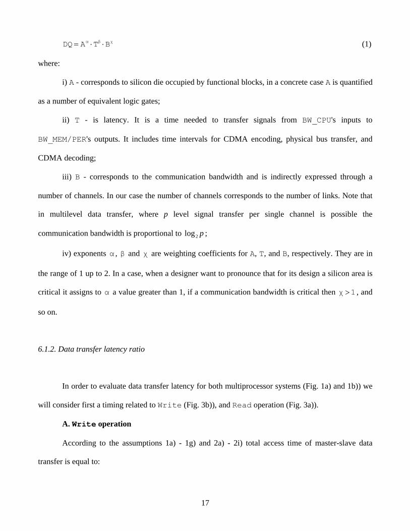
(1) χβα BTADQ
where:
i) A - corresponds to silicon die occupied by functional blocks, in a concrete case A is quantified
as a number of equivalent logic gates;
ii) T - is latency. It is a time needed to transfer signals from BW_CPU's inputs to
BW_MEM/PER's outputs. It includes time intervals for CDMA encoding, physical bus transfer, and
CDMA decoding;
iii) B - corresponds to the communication bandwidth and is indirectly expressed through a
number of channels. In our case the number of channels corresponds to the number of links. Note that
in multilevel data transfer, where p level signal transfer per single channel is possible the
communication bandwidth is proportional to ; p2log
iv) exponents α , β and are weighting coefficients for A, T, and B, respectively. They are in
the range of 1 up to 2. In a case, when a designer want to pronounce that for its design a silicon area is
critical it assigns to α a value greater than 1, if a communication bandwidth is critical then , and
so on.
χ
1χ
6.1.2. Data transfer latency ratio
In order to evaluate data transfer latency for both multiprocessor systems (Fig. 1a) and 1b)) we
will consider first a timing related to Write (Fig. 3b)), and Read operation (Fig. 3a)).
A. Write operation
According to the assumptions 1a) - 1g) and 2a) - 2i) total access time of master-slave data
transfer is equal to:
17

18
i) Standard system (Fig. 1a)): When there is single issue for master-slave data transfer, a
request will be served for
TTS1W = tP + tBA + tD + tACC (2)
by substituting for tBA 7tP, tD = 2tP, and tACC = 20tP, we obtain
TTS1W = 30tP
When all k master modules issue requests for data transfer, the access time, TTSW, will be proportional
to k, i.e.
TTSW = k * TTS1W = k * 30tP (3)
ii) CDMA based system (Fig. 1b)): In this case all k master-slave connections are performed
simultaneously for
TTCW = tP + tBA + tCDMA + tACC = 28tP + tCDMA (4)
where tCDMA is a time interval which corresponds to a total latency given in Table 1.
B. Read operation
In a similar way, for a Read operation (see Fig. 3a)) we obtain:
j) Standard system (Fig. 1a)):
TTS1R = 2*tP + 2*tBA + tD + tACC = 38tP (5)
TTSR = k * TTS1R = k * 38tP (6)
jj) CDMA based system (Fig. 1b)):
TTCR = 2*tP + 2*tBA + 2*tCDMA + tACC = 36tP + 2*tCDMA (7)
Let note that for establishing master-slave data transfer the system from Fig. 1a) uses TDMA
approach, while the system from Fig. 1b) explores parallelism.
Metrics Q and R
Form now a performance metric, Q, as a product of the following three parameters: a) a number
of bus lines, L; b) total access time, T; and c) communication bandwidth, B:

(8) BTLQ
For the standard system (Fig. 1a)) and CDMA bus based system (Fig. 1b)), respectively, we have:
(9) 1TSX11X BTLQ
and
(10) 2TCX22X BTLQ
where a subscript X can be W for Write operation, or R for Read operation.
Let B1 = B2 (i.e. an equal amount of information is transferred by both systems), and define
now a data transfer ratio for Write and Read operation, RW, and RR, respectively as
TCW2
TSW1
2W
1WW TL
TL
Q
Q R
(11)
and
TCR2
TSR1
2R
1RR TL
TL
Q
Q R
(12)
In the aspect of data transfer rate performance we will use data transfer ratio, RW and RR, as
convenient range indices by which we will evaluate the increased latency of the CDMA simultaneous
master slave data transfer (Fig. 1b)) in respect to a sequential TDMA bus transfer (Fig. 1a)).
7. Experimental results
Increasing demand for high-speed on-chip interconnects requires faster links that consume less
power. Signal coding is a standard approach used to lower the bus width, achieve low signaling rate,
and find a low-power scheme. However, the complexity of those coding systems (transmitter and
receiver hardware with micro-power consumption) prohibits their use in high-speed on-chip
applications. An on-chip interconnect scheme based on CDMA technique of relatively low complexity,
19

20
low-power, and high bandwidth is proposed here and its performance related to design quality of a
wrapper logic and data transfer latency are evaluated.
7.1. Wrapper logic performance
The wrapper logic was described at RTL level using VHDL. For synthesis, routing, and
mapping a Xilinx development CAD tool ISE WebPack 9.1i was used. Design verification was
performed using testbenches intended for parallel excitation of all bundle links. The wrapper was
implemented on FPGA devices from Spartan2, Spartan3, Virtex4, Virtex5, and VirtexE series. The
results generated by a CAD tool relate to: a) a number of equivalent gates, or logic cells, which is
proportional to the occupied silicon area; b) a signal propagation time which corresponds to the total
latency of a communication channel, i.e. the time interval t12, sketched in Fig. 3; and c) the dissipated
power in mW for a given operating frequency.
7.1.1. Absolute performance
The obtained results that correspond to absolute quantitative performance values are presented
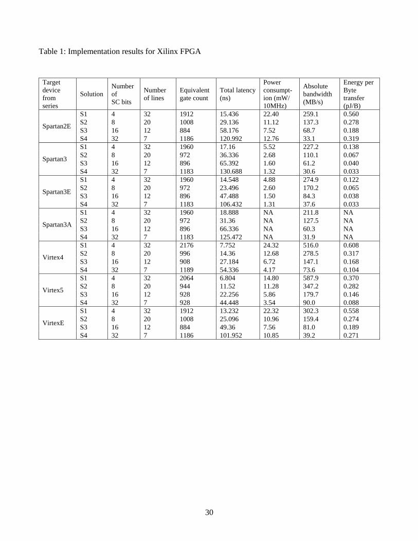
in Table 1. For a given target device, in each row of Table 1, a corresponding column specifies:
a1) Solution – a type of bundle (connection with parallel lines - eight-, four-, two-, and single-
bundle);
a2) Number of SC bits – a number of spreading code bits needed for encoding a corresponding
bundle of parallel lines;
a3) Number of lines – a number of transmission lines (links) of the CDMA coded bus which
equivalently corresponds to the number of bus lines for binary coded 32-bit bus (see Fig. 1b)):

21
a4) Equivalent gate count - corresponds to the number of equivalent gates needed for
implementation of a master, BW_CPU, and a slave, BW_MEM/PER, wrappers, i.e. the logic of a wrapper
pair.
a5) Total latency – total propagation delay which includes signal propagation through a master
wrapper, a slave wrapper and a CDMA Shared System Bus (time interval tCDMA in Fig. 3).
a6) Power consumption – dissipated power of a wrapper logic pair (transmitter and receiver) at 10
MHz clock period excitation.
a7) Absolute bandwidth – a bandwidth achieved at maximal operating frequency, in megabytes
per second, for a given FPGA circuit.
a5) Energy per byte transfer – consumed energy per single byte transfer.
Table 1: Implementation results for Xilinx FPGA
In general, according to the obtained results presented in Table 1 we can conclude the
following:
1. For all design solutions, by increasing the width of a spreading code, what is equivalent to
decreasing a number of bundles, the number of lines of a CDMA coded bus decreases, but the latency
increases.
2. For each master-slave wrapper the number of equivalent logic gates has its minimum when
orthogonal spreading codes of width from 8 up to 16 bits are used.
3. The consumed energy per byte transfer decreases as the number of lines for data transfer decreases,
i.e. in a concrete case for Solution S4 in most design solutions we obtain minimal or near-minimal
energy consumption. Such results are direct consequence of hardware overhead for CDMA coding.
4. The communication bandwidth is always highest for Solution S1 and smallest for S4, mainly due to
larger number of lines, 32 versus 7, and shorter chip sequences, 4 in contrast to 32.
5. In our opinion the consumed energy per byte transfer is relatively low. It is in the range of 0.0888
pJ/B (for target device from series Virtex5 Solution S4) up to 0.608 pJ/B (for target devices from series
Virtex4 Solution S1).
6. Data transfer rates are relatively high and are in the range of 587.9 megabytes per second (for target
device from series Virtex5 Solution S1) down to 30.6 megabytes per second (for target device from
series Spartan3 Solution S4).
7. From the aspect of latency, wrapper’s implementations for new generation FPGA devices (Virtex4
and Virtex5) have superior performance in respect to identical architectural implementations that are
distinctive for FPGA devices of older generations (Spartan2, and Spartan3). For example, in a worst
case, the latency ratio between a device from Spartan3 series and a device from Virtex5 series is equal
to 94244844688130 ... . So, when a signal propagation of a design is critical better choice are
wrappers implemented in new generation FPGA devices. From the other hand, from aspect of occupied
silicon area, for a ratio which corresponds to a number of equivalent logic gates we obtain a value
which is equal to 2719281183 . . This result implies that the impact of using new technology is not
so pronounced, as was the case with a latency ratio, what means that hardware structures of logic cells
in Spartan and Virtex series are similar.
7.1.2. Relative performance
For relative performance evaluation of a master-slave wrapper pair a metric DQ was used. For
four different connections with parallel lines (eight-, four-, two-, and single-bundle) performance
parameters which correspond to a number of links (CDMA channels), a number of equivalent logic
gates, and total latency are given in Table 1. In order to simplify our analysis and result presentation,
but without deteriorating its generality, we have further assumed that . Performance 1χβα
22

23
parameters A, T, and B that take part in forming DQ (see Fig. 5) were normalized in respect to their
maximal values for all devices series and all solutions (for example, for Spartan2E series maximal
value for A is 1912 gates, for T it is 120.992 ns, and for B it corresponds to 32 lines, see Table 1). The
normalization was used with aim to evaluate a wrapper architectural quality, which takes into account
the encoding complexity of a CDMA coded bus for different bus width, i.e. the number of bundles.
Figure 5. Dependencies of A, T, B, and DQ in terms of spreading code for target devices from series:
a) Spartan2E, b) Spartan3, c) Spartan3E, d) Spartan3A, e) Virtex4, f) Virtex5, g) VirtexE
In Fig. 5 diagrams that show the dependencies of A, T, B, and DQ in terms of a spreading code
width for several FPGA devices implemented in different technology series (Spartan, Virtex) are
presented. By analyzing Fig. 5 we can derive the following conclusions:
a) In all wrapper designs, tendency of changes, which relate to the normalized values of A, T, B, and
DQ, are almost identical, what means that the optimal wrapper architecture doesn't depend on a selected
FPGA technology.
b) In all design solutions the maximal variations of a DQ metric are relatively small, and are in the
range of 8% up to 10%, what means that for all design solutions good design balance was achieved.
c) A minimal value of DQ metric, for all design solutions, we obtain for width of spreading code in the
range of 8 up to 16 bits.
7.2. Data transfer latency performance
Table 2 reports the results which relate to data transfer latencies for standard and CDMA bus
based systems. For implementation of a wrapper logic FPGAs from Spartan2E, Virtex4 and Virtex5
series were used. Multiprocessor systems composed of 2, 4, 8, and 16 master and slave modules were

24
considered. We assumed that all master modules simultaneously access to different slave modules, i.e.
a contention problem was omitted. This means that the presented results correspond to maximal data
transfer rate. During this analysis we assumed that bus requests issued by master module in Fig. 1a) are
served in a circular way, i.e. fixed time slot bus allocation scheme was used.
Data transfer rates for Write and Read operations were derived. Having in mind the number
of I/O pins and logic capacity of FPGAs, as well as the capacity loading of a standard and CDMA bus
(direct consequence of wiring) only the results which correspond from 2 to 16 processor systems have a
sense.
Table 2: Data transfer ratio for Write and Read operations
Notice: tp = 1.5 ns; Column referred as Number of lines includes address and data bus lines.
By analyzing the results given in Table 2 we can conclude the following:
1) Spartan2E series: transfer rates for Write operations are from 28% (for 2-processor systems) to 6%
(for 16-processor systems) faster for CDMA based bus architecture in respect to standard bus
architecture. Contrary, transfer rates for Read operations standard bus architecture is faster from 23%
to 32%.
2) Virtex4 and Virtex5 series: for both Write and Read operations performance related to data
transfer rates for CDMA based bus architecture in respect to standard bus architecture are superior.
Namely, for Virtex4 Write operations are from 126% to 108% and Read operations are from 54% to
34% faster, while for Virtex5 Write operations are from 188% to 172% and Read operations are
from 96% to 78% faster.
Let note that the results given in Table 2 are illustrative only. Other factors such as bus
allocation policy, physical bus wiring limitations, propagation delay involved by a complexity of the
bus arbiter, burst mode of bus transfer, etc. have to be considered in real applications.
25
In general, the results given in Table 1 and 2 show that: a) involvement of CDMA bus based
system is a trade-off problem between decreased number of bus lines and communication time and it
may appeal to applications where bus size (wiring) reduction is imperative; and b) increased data
transfer latencies involved by CDMA data transfer are compensated by simultaneous master-slave
transfers.
8. Conclusion
Traditionally, design-space exploration for SoCs has been focused on the computational aspects
of the problem at hand. However, integrating an increasingly large number of IP cores on the same chip
make the design of communication architectures for future SoCs a challenging problem. As a result,
design-space exploration with emphasis on communication aspects becomes crucial. Towards this end,
in this article we have described a binary CDMA wrapper based bus implementation that has
acceptable performance with low hardware cost. Two types of wrappers can be identified, a master
located at the output of a bus arbiter in MPSoC and a slave accompanied to memory/peripheral
modules. With aim to combine the positive attributes of smaller address and data buses as well as to
achieve control bus compliance with existing bus conversion protocols such as AMBA to BVCI or
PVCI or others we have proposed a CDMA encoding technique both for address and data buses, but
not for a control bus. The proposed solution utilizes orthogonal CDMA coding and a variation of
source synchronous clocking in order to achieve channels separation without interference.
Reconfiguration of the CDMA coded bus system is achieved by simply re-assigning the spreading code
during the FPGA configuration phase. At behavioral level a wrapper structure was described using
VHDL code. For synthesis, routing, and technology mapping a Xilinx development CAD tool ISE
WebPack 9.1 was used. The wrapper was implemented on FPGA devices from Spartan and Virtex
series. Crucial design factors which include: a) absolute quantitative performance metrics such as the

26
number of equivalent logic gates, power consumption, absolute bandwidth, consumed energy per byte
transfer, and communication latency; and b) a relative metric DQ relevant to evaluate the proposed
design, were derived. These metrics were used to analyze the quality of four different design solutions
of the proposed FPGA communication architectures. We involved too, convenient range indices called
RW and RR to determine data transfer rate for Write and Read operations in multiprocessor bus
systems that use TDMA and CDMA data transfer techniques. In addition, let note that increased data
transfer latencies involved by CDMA data transfer are compensated by simultaneous master-slave
transfers.
In general, like other optimization technique, we always have a trade-off. Here, trade-off is
decreased number of bus lines for better wiring performance.
We suspect that there remains further room for improvement, especially multilevel signaling
can be used to reduce the number of signal paths and/or to increase the data rate.
Acknowledgements
This work was supported by the Serbian Ministry of Science and Technological Development,
project No. TR - 11020 - "Reconfigurable embedded systems".
References
[1] Pasricha S, Dutt N. On-chip communication architectures: system on chip interconnect. Amsterdam: Elsevier Inc; 2008 [2] Kim J, Verbauwhede I, Chang MCF. Design of an interconnect architecture and signaling technology for parallelism in communication. IEEE Trans on VLSI Systems 2007;15(8):881-94

27
[3] Mak TST, Sedcole P, Cheung PYK, Luk W. On-FPGA communication architectures and design factors. In: Proc. International Conference on Field Programmable Logic and Applications, Madrid; 2006, p. 1-8 [4] Dey S, Lahiri K, Raghunathan A. Design of communication architectures for high-performance and energy-efficient systems-on-chips. In: Jerraya AA, Wolf W, editors. Multiprocessor Systems-on-Chips, San Francisco: Morgan Kaufman; 2005, p. 187-222 [5] Mitic M, Stojcev M. An overview of on-chip buses. Facta Universitatis, Series: Electronics and Energetics 2006; 19(3):405-28 [6] Benini L, De Micheli G. Networks on chips: A new paradigm for component based MPSoC design. In: Jerraya AA, Wolf W, editors. Multiprocessor Systems-on-Chips, San Francisco: Morgan Kaufmann; 2004, p. 187-222 [7] ibid. Networks on chips: Technology and tools. Amsterdam: Elsevier; 2006. [8] Jantsch A, Tenhunen H, Introduction. In: Jantsch A, Tenhunen H, editors. Networks on chip. Boston: Kluwer Academic Publishers; 2003, p. 1-24 [9] Anjo K, Okamura A, Motomura M. Wrapper-based bus implementation techniques for performance improvement and cost reduction. IEEE Journal of Solid-State Circuits 2004;39(5):804-17 [10] Lysecky R, Vahid F. Pre-fetching for improved bus wrapper performance in cores. ACM Transaction on Design Automation of Electronic Systems (TODAES) 2002;7(1):58-90 [11] Wu KL, Jou JM, Shiau YH. Bus wrapper design methodology in the SoC. In: Proceedings of the 2002 VLSI Design/CAD Symposium; 2002. p. 524-7, also [Online], available at http://etdncku.lib.ncku.edu.tw, July 2008 [12] Lai BC, Schaumont P, Verbauwhede I. CT-bus: A heterogeneous CDMA/TDMA bus for future SoC. In: Proc. 38th Annu. Asilomar Conference on Signals, Systems, and Computers; 2004, Vol. 2, p. 1868-72 [13] Wang X, Ahonen T, Nurmi J. Applying CDMA technique to network-on-chip. IEEE Transactions On Very Large Scale Integration (VLSI) Systems 2007;15(10):1091-100 [14] Bell Jr RH, Chang KY, John L, Swartzlander Jr EE. CDMA as a multiprocessor interconnect strategy. In Conf. Record of 35th Asilomar Conf. Signals, Syst. Comput., 2001. p. 1246–50 [15] Yuminaka Y, Katoh O, Sasaki Y, Aoki T, Higuchi T. An efficient data transmission technique for VLSI systems based on multiple-valued code-division multiple access. In: Proceedings of IEEE International Symposium on Multiple-Valued Logic; 2000. p. 430-7 [16] Nikolic T, Djordjevic G, Stojcev M. Simultaneous data transfers over peripheral bus using CDMA technique. In: Proceedings of 26th International Conference on Microelectronics, MIEL, Nis 2008. Vol. 2. p. 437-40

28
[17] ARM AMBA Specification and multi-layer AHB specification (rev 2.0), [Online], available at http://www.arm.com, July 2008 [18] IBM CoreConnect specification, [Online], available at http://www.ibm.com/chips/techlib.nsf/productfamilies/CoreConnect_Bus_Architecture, July 2008 [19] STBus communication systems: Concepts and definitions. Reference Guide, STMicroelectronics, May, 2003 [20] IBM Inc. Blue logic technology, [Online], available at http://www.chips.ibm.com/blue-logic/, July 2008 [21] Virtual Socket Interface Alliance, [Online], available at http://www.vsi.org, July 2008 [22] Xilinx Inc., San Jose, CA., Virtex-4 family overview, 2007, [Online], available at http://www.xilinx.com/bvdocs/publications/ds112.pdf, July 2008 [23] El-Guibaly F. Design and analysis of arbitration protocols. IEEE Transactions on Computers 1989;38(2):161-71 [24] Poletti F, Bertozzi D, Benini L, Bogliolo A. Performance analysis of arbitration policies for SoC communication architectures. Journal of Design Automation for Embedded Systems 2003;8:189-210 [25] van Baelen S., The interface Wrapper Architecture, ITEA, December 2003, [Online], available at http://www.empress-itea.org/deliverables/D2.1-2.2_Appendix_C_v1.0_Public_Version.pdf, July 2008 [26] Wang LT, Stroud CE, Touba NA. Introduction-Chapter 1. In: Wang LT, Stroud CE, Touba NA, editors. System on chip test architectures. Boston: Morgan Kaufmann Publishers; 2008, p. 1-40 [27] Cesario WO, Jerraya AA. Component-based design for multiprocessor systems-on-chips. In: Jerraya AA, Wolf W, editors. Multiprocessor systems-on-chips, Boston: Morgan Kaufmann Publishers; 2005, p. 357-93 [28] Lysecky RL, Vahid F, Givargis TD. Experiments with peripheral virtual component interface. In: Proceedings of the 13th International Symposium on Systems Synthesis, Madrid, 2000, p. 221-4

29
Captures for Figures Figure 1. Multiprocessor systems based on: a) standard bus transfer; b) CDMA transmission technique
Figure 2. BW_CPU wrapper structure
Figure 3. Timing of a Read and Write processor cycles: a) signaling scenario of a Read processor cycle; and b) signaling scenario of a Write processor cycle Figure 4. Four different parallel lines configurations: a) eight bundles; b) four bundles; c) two bundles; and d) single bundle Figure 5. Dependencies of A, T, B, and DQ in terms of spreading code for target devices from series: a) Spartan2E, b) Spartan3, c) Spartan3E, d) Spartan3A, e) Virtex4, f) Virtex5, g) VirtexE Capture for Table Table 1 Implementation results for Xilinx FPGA Table 2: Data transfer ratio for Write and Read operations
Notice: tp = 1.5 ns; Column referred as Number of lines includes address and data bus lines.
30
Table 1: Implementation results for Xilinx FPGA
Target device from series
Solution Number of SC bits
Number of lines
Equivalent gate count
Total latency (ns)
Power consumpt- ion (mW/ 10MHz)
Absolute bandwidth (MB/s)
Energy per Byte transfer (pJ/B)
S1 4 32 1912 15.436 22.40 259.1 0.560 S2 8 20 1008 29.136 11.12 137.3 0.278 S3 16 12 884 58.176 7.52 68.7 0.188
Spartan2E
S4 32 7 1186 120.992 12.76 33.1 0.319 S1 4 32 1960 17.16 5.52 227.2 0.138 S2 8 20 972 36.336 2.68 110.1 0.067 S3 16 12 896 65.392 1.60 61.2 0.040
Spartan3
S4 32 7 1183 130.688 1.32 30.6 0.033 S1 4 32 1960 14.548 4.88 274.9 0.122 S2 8 20 972 23.496 2.60 170.2 0.065 S3 16 12 896 47.488 1.50 84.3 0.038
Spartan3E
S4 32 7 1183 106.432 1.31 37.6 0.033 S1 4 32 1960 18.888 NA 211.8 NA S2 8 20 972 31.36 NA 127.5 NA S3 16 12 896 66.336 NA 60.3 NA
Spartan3A
S4 32 7 1183 125.472 NA 31.9 NA S1 4 32 2176 7.752 24.32 516.0 0.608 S2 8 20 996 14.36 12.68 278.5 0.317 S3 16 12 908 27.184 6.72 147.1 0.168
Virtex4
S4 32 7 1189 54.336 4.17 73.6 0.104 S1 4 32 2064 6.804 14.80 587.9 0.370 S2 8 20 944 11.52 11.28 347.2 0.282 S3 16 12 928 22.256 5.86 179.7 0.146
Virtex5
S4 32 7 928 44.448 3.54 90.0 0.088 S1 4 32 1912 13.232 22.32 302.3 0.558 S2 8 20 1008 25.096 10.96 159.4 0.274 S3 16 12 884 49.36 7.56 81.0 0.189
VirtexE
S4 32 7 1186 101.952 10.85 39.2 0.271

31
Table 2: Data transfer ratio for Write and Read operations
Traditional system CDMA based system Target device from series
Number of
masters Number of lines
Access time, TTSW
Access time, TTSR
Number of lines
Total access
time, TTCW
Total access time,
TTCR
Data
transfer ratio, RW
Data
transfer ratio, RR
2 64 60 tp 76 tp 16 188 tp 356 tp 1.28 0.86 4 64 120 tp 152 tp 18 348 tp 676 tp 1.22 0.80 8 64 240 tp 304 tp 20 668 tp 1316 tp 1.14 0.74
Spartan2E
16 64 480 tp 608 tp 22 1308 tp 2596 tp 1.06 0.68 2 64 60 tp 76 tp 16 108 tp 196 tp 2.22 1.54 4 64 120 tp 152 tp 18 188 tp 356 tp 2.26 1.52 8 64 240 tp 304 tp 20 348 tp 676 tp 2.20 1.44
Virtex4
16 64 480 tp 608 tp 22 668 tp 1316 tp 2.08 1.34 2 64 60 tp 76 tp 16 88 tp 156 tp 2.72 1.94 4 64 120 tp 152 tp 18 148 tp 276 tp 2.88 1.96 8 64 240 tp 304 tp 20 268 tp 516 tp 2.86 1.88
Virtex5
16 64 480 tp 608 tp 22 508 tp 996 tp 2.74 1.78
Notice: tp = 1.5 ns; Column referred as Number of lines includes address and data bus lines.

Fig. 1a)
Fig. 1b)
32

Fig. 2.
Fig. 3a)
33
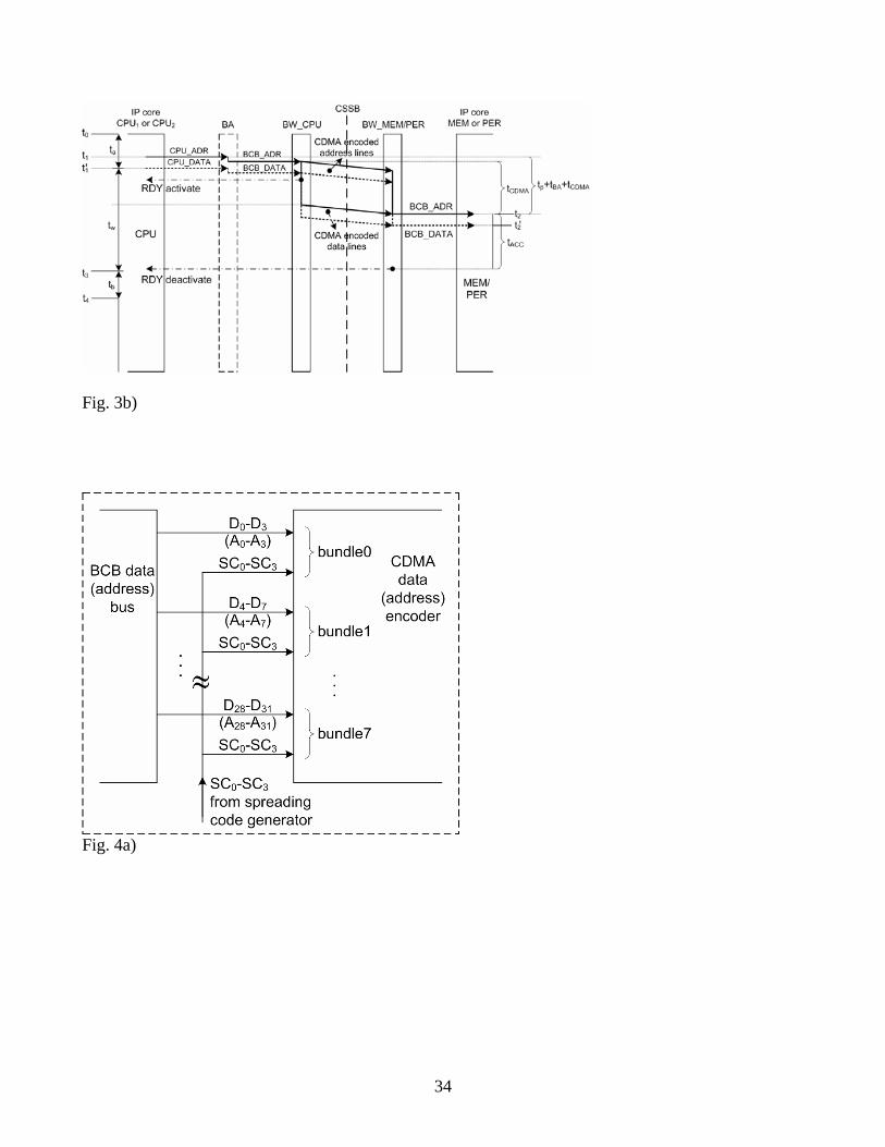
Fig. 3b)
Fig. 4a)
34

Fig. 4b)
Fig. 4c)
Fig. 4d)
35

Fig. 5a)
Fig. 5b)
Fig. 5c)
36

Fig. 5d)
Fig. 5e)
Fig. 5f)
37

Fig. 5g)
Fig. 5 legend
38