Carvey PCB Milling Project - Amazon Web Services · PDF fileCarvey PCB Milling Project ......
10
Carvey PCB Milling Project The goal for this project is to use only a stock Carvey setup with no mods, and nothing purchased except cutting tools and FR1 material and a wasteboard. Note, I already had a software tool to capture a schematic, layout a pcb and produce gerber files. Stuff I used 1. Carvey router and Easel software 2. Target 3001 (free version available) schematic capture, pcb layout software to generate gerber files, 3d model generation 3. FlatCAM (free) to convert gerber to gcode 4. Inventables PCB Milling Bits (used 20 deg 0.2mm V tool) 5. Inventables PCB Drill Set (used .031”, 039” for component holes) 6. Inventables 1/16 Flat End Mill to clear no copper areas, and drill large holes 7. Double-sided tape 8. 1/4” thick 6” wide popular for a waste board. Cut to just under the size of the FR1 material which is 4”x6” Just got my Carvey and one important job for this little puppy is to make prototype PCBs. I use through hole, SOIC and 1206 size SMDs so they don’t have super small features. For PCB design software I been using both DipTrace and Target 3001 for quite a few years. In this case I worked with Target because my pcb will eventually have to go into a small enclosure made on my 3D printer and I wanted a 3D step file output. DipTrace can do it, but I never can find the 3D models for the parts I’m using. I tried building a 3D model in my CAD software and importing into DipTrace but there were scaling issues and I didn’t feel like working through those issues. Target on the other hand has a simple built-in 3D model making capability. The circuit I’m making is to control an LED grow light and has a couple touch controls and status led and buzzer. A PIC16F controller provides enough I/O and drive capacity; and has PWM functionality to manage the LED intensity. Since this LED light will be passively cooled, an important function of this controller is to monitor the temperature at the heatsink and dim the LEDs if things get too hot. A 24V DC adapter provides power through a 5.5/2.5mm jack. A 5V regulator provides low voltage for the controller functions. Screw terminals provide IO to the LED driver modules which are not mounted on the board itself and to the thermistor which is off course mounted on the heatsink. The ICSP header allows me to program the controller with a PICkit3. Below is a 3D model of the PCB as generated in Target. By default the model is shown with a green solder mask and silk screen which obviously won’t be on the milled pcb.
Transcript of Carvey PCB Milling Project - Amazon Web Services · PDF fileCarvey PCB Milling Project ......
Carvey PCB Milling Project The goal for this project is to use only a stock Carvey setup with no mods, and nothing purchased except cutting tools and FR1
material and a wasteboard. Note, I already had a software tool to capture a schematic, layout a pcb and produce gerber files.
Stuff I used 1. Carvey router and Easel software 2. Target 3001 (free version available) schematic capture, pcb layout software to generate gerber files, 3d model
generation 3. FlatCAM (free) to convert gerber to gcode 4. Inventables PCB Milling Bits (used 20 deg 0.2mm V tool) 5. Inventables PCB Drill Set (used .031”, 039” for component holes) 6. Inventables 1/16 Flat End Mill to clear no copper areas, and drill large holes 7. Double-sided tape 8. 1/4” thick 6” wide popular for a waste board. Cut to just under the size of the FR1 material which is 4”x6”
Just got my Carvey and one important job for this little puppy is to make prototype PCBs. I use through hole, SOIC and 1206
size SMDs so they don’t have super small features. For PCB design software I been using both DipTrace and Target 3001 for
quite a few years. In this case I worked with Target because my pcb will eventually have to go into a small enclosure made on
my 3D printer and I wanted a 3D step file output. DipTrace can do it, but I never can find the 3D models for the parts I’m using.
I tried building a 3D model in my CAD software and importing into DipTrace but there were scaling issues and I didn’t feel like
working through those issues. Target on the other hand has a simple built-in 3D model making capability.
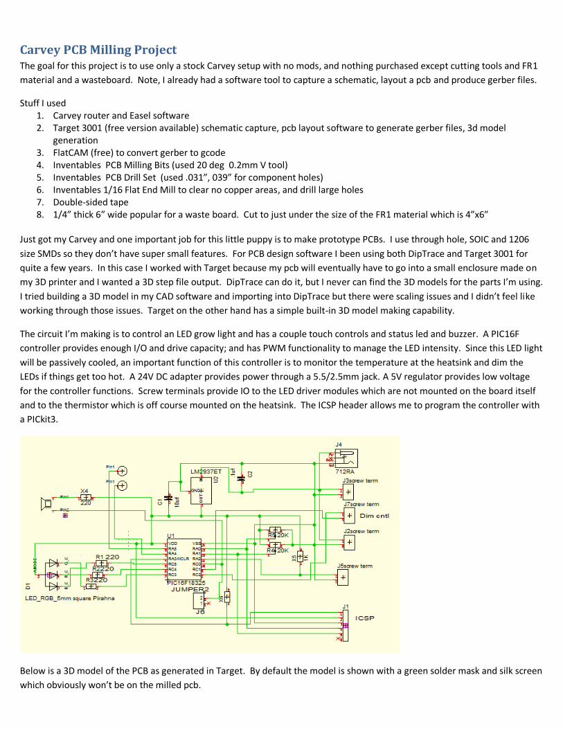
The circuit I’m making is to control an LED grow light and has a couple touch controls and status led and buzzer. A PIC16F
controller provides enough I/O and drive capacity; and has PWM functionality to manage the LED intensity. Since this LED light
will be passively cooled, an important function of this controller is to monitor the temperature at the heatsink and dim the
LEDs if things get too hot. A 24V DC adapter provides power through a 5.5/2.5mm jack. A 5V regulator provides low voltage
for the controller functions. Screw terminals provide IO to the LED driver modules which are not mounted on the board itself
and to the thermistor which is off course mounted on the heatsink. The ICSP header allows me to program the controller with
a PICkit3.
Below is a 3D model of the PCB as generated in Target. By default the model is shown with a green solder mask and silk screen
which obviously won’t be on the milled pcb.

Since it was my first milled pcb I made this a single sided layout so I didn’t have to deal with registration accuracy issues
between features on the two surfaces. Eventually all the resistors and caps will be surface mount but since this pcb is for
debugging and I wanted some easy access to probe signals, I used through hole.
I wasn’t sure how fine of features the Carvey could produce reliably, so I doubled the standard trace width in Target. The
default is 12 mils and I set it to 24mils for normal signal traces and 36 mils for those traces supplying power to the LED drivers.
Since the board will be single-sided and I won’t be able to access under the screw terminals to solder them, they will be have
to be mounted on the bottom side. I think all other components can be soldered on the top with the possible exception of the
trim pots.
I had to manually adjust many of the traces to provide a separation area around the touch pads and because the router
included with Target could not complete the routing job with all the limitations I gave it. In the end there were 3 air wires.
The Gerber export function can export many different files, but only 3 files are needed for this board; the .TOP file containing
the trace pattern, the .DRILL file containing drill sizes and coordinates and the .OUTLINE file which contains the board outline.
Isolation Carving After reviewing what others had used as middle ware to crunch Gerber files into cnc format, I decided to use FlatCAM to
produce gcode from the gerber files. In general it seems very straightforward to use although I did hit a couple glitches while
working through this pcb. I was able to work around each issue and continue the project. I started by using File/Open Gerber
and selected the Cntl.Top gerber file. The software keeps a list of your original gerber files, and all geometry and cnc data file
that it produces appear in a list under the Tab labelled Project. Basically, you select a file in the Project list and perform
operations on that data in the Selected Tab and generate a new ‘geometry’ file. From the geometry file, you can produce a
‘cnc’ file and from that you can export a gcode file which can be imported to Easel.
I selected the Cntl.TOP file in the Project list and then went to the Selected tab, which shows the heading “Gerber Object”. At
this point I can see the contents of the Gerber .TOP file plotted in the graph area at right and several sections of control
settings on the left panel.

A very important first step is to offset the data in the Gerber file. The Gerber file produced by Target has its origin X=0, Y=0 at
the lower left corner of the plot. But the Smart clamp system of the Carvey will not allow any work to be performed in the
lower left corner of the pcb material. In FlatCAM the very bottom of the left panel contains controls to offset the plot. I
entered the values 25.4, 25.4mm which corresponds to a 1in offset in x and y. Pressing Offset caused the plot to shift up and
to the right the desired amount.
I had chosen the 0.2mm 20 deg V bit for isolation routing so I set the tool diameter at 0.3 (make sure that units are set to ‘mm’
in the Options tab) and selected 1 for the Width (1 pass) and left the Pass overlap alone since that only applies if there are 2 or
more passes. The reason for the tool diameter being set to 0.3 instead of 0.2 is that with a cutting depth of .2mm and the 20
deg taper I estimated that the width of the tool could be as high as .29mm given the amount of variation in the height of the
pcb surface.
Pressing Generate Geometry in the Isolation Routing section produces a new entry in the project panel labeled Cntl.Top_iso
which contains outline geometry data for the top copper. Now I have to go back to the Project tab, select this new entry
‘Cntl.Top_iso’ and then go back to the Selected tab (which now has a heading Geometry Object) to perform a function with
that data. The first thing I did was to rename this project file to Cntl.Top_iso_OutlineV20_0_2mm. The entire project will have

as many as 10 files and I want them to be clearly identifiable by the name. The plot at right now shows the original green
traces with a red outline showing the tool path calculated by FlatCAM. In this case what I want to do is generate a gcode file
containing the tool path to cutout around each trace. Several values have to be set before generating the cnc data.
Cut Z is how deep to cut. The PCB is ~1.5mm thick and the copper is only about .04mm thick, so you would think a depth like
.05mm would work. I did test cuts at several increasing depths and found that over the area of my 2.5” x 3.5” plot I had to
increase the depth to 0.2mm depth to get a clean isolation all around. Originally I was going to probe the surface heights
using Chilipepper and techniques others have described, but I decided to work out a process using just the Easel software.
Travel Z is the height to lift the tool when moving across the board surface between cuts. Feed Rate is how fast to move the
head. Tool dia is the diameter at the tip. I left Spindle speed empty which I believe causes the spindle to run at max speed. The
image above shows the settings I used. After completing my pcb I noticed that Easel defaults to 254mm/min feed rate for PCB
material which is alot faster, and I’ll change to that next time.
Pressing the Generate button below these entries produces another entry in the Project list, and after selecting that item, the
left panel label changes to CNC Job Object. Finally we can produce a G-code file by pressing the Export G-Code button at the
bottom of the left hand panel (not shown in the screen capture). You can call the file anything you want since the file name
and type don’t matter to Easel when you import a gcode file, however it is a very good idea to have enough information in the
file name to know which tool it was created for.
Unfortunately, Easel won’t accept this file directly because of a tiny formatting issue, but one that is a pain in the neck to have
to manually correct each time. Below are shown two gcode files. The one on the right is as produced by FlatCAM, and the one
on the left after modifying it so Easel will accept it. Each Gcode command is a letter followed by 1 or 2 numbers. On the right
hand file, I’ve added a few notes to show the meaning of the commands. You will notice that the right hand file (produced by
FlatCAM) always has 1 letter followed by 2 number digits such as G00, M03, G04, etc. The leading zero on these commands is
not accepted by Easel; it will flag them as invalid gcode commands. So…. You have to manually edit the file, like I did to the
one on the left, using the editor Replace function to replace G01 with G1 and likewise modify all the other commands that
have leading zeros.
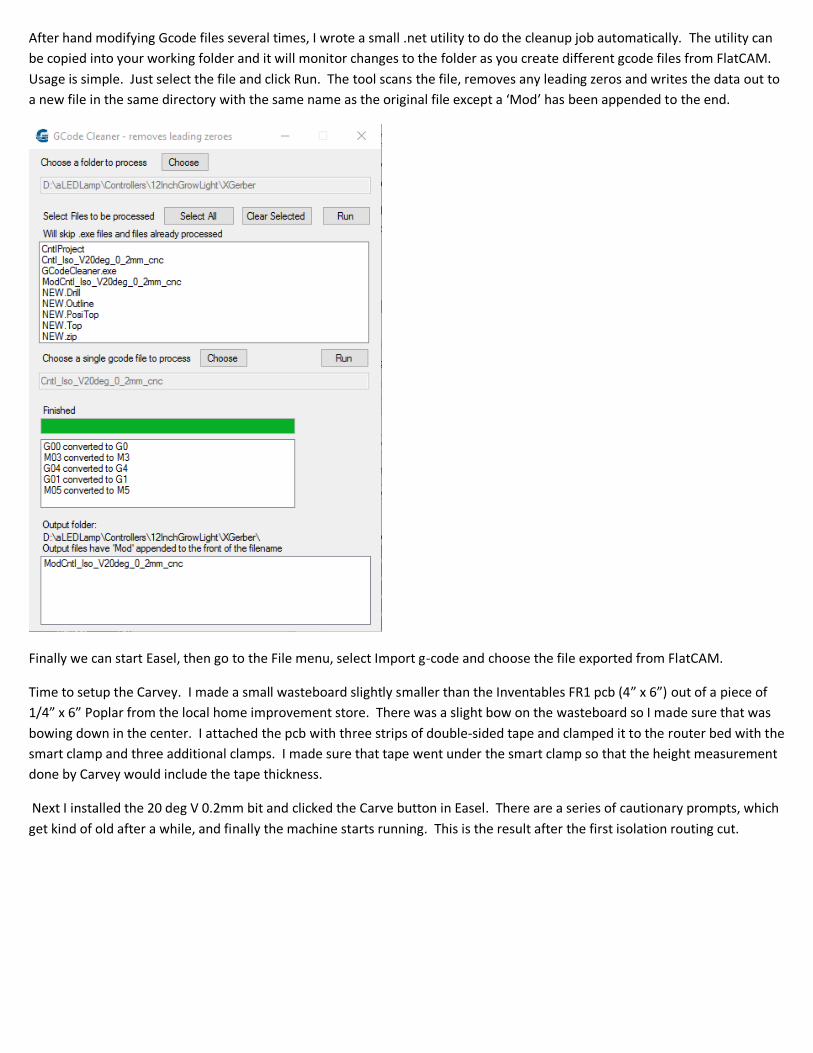
After hand modifying Gcode files several times, I wrote a small .net utility to do the cleanup job automatically. The utility can
be copied into your working folder and it will monitor changes to the folder as you create different gcode files from FlatCAM.
Usage is simple. Just select the file and click Run. The tool scans the file, removes any leading zeros and writes the data out to
a new file in the same directory with the same name as the original file except a ‘Mod’ has been appended to the end.
Finally we can start Easel, then go to the File menu, select Import g-code and choose the file exported from FlatCAM.
Time to setup the Carvey. I made a small wasteboard slightly smaller than the Inventables FR1 pcb (4” x 6”) out of a piece of
1/4” x 6” Poplar from the local home improvement store. There was a slight bow on the wasteboard so I made sure that was
bowing down in the center. I attached the pcb with three strips of double-sided tape and clamped it to the router bed with the
smart clamp and three additional clamps. I made sure that tape went under the smart clamp so that the height measurement
done by Carvey would include the tape thickness.
Next I installed the 20 deg V 0.2mm bit and clicked the Carve button in Easel. There are a series of cautionary prompts, which
get kind of old after a while, and finally the machine starts running. This is the result after the first isolation routing cut.

Second Isolation Outline
Photo below is after 3 isolation passes; each one was set with an increasing tool width to move the carve line out further from
the actual trace outline.

Removing non-copper areas. Next I choose the original Cntl.TOP project entry and entered a Boundary Margin and used Generate Geometry to create a new
geometry object which is simply a border containing all the geometry to this point plus the entered margin.
Selecting that new geometry object (Cntl.Top_noncopper). The left panel top section is labelled ‘Create CNC Job’ and the next
panel down is ‘Paint Area’. The sequence we need to use is to first generate a Paint pattern geometry and then create a cnc
job from that.
I set a tool diameter of 1.58mm which corresponds to the 1/16” flat mill which came with the Carvey. Overlap is the amount
each tool path cut will overlap the previous cut. Margin is how far to stay away from the trace outline. When creating a Paint
pattern, you first click the Generate button below the Paint Area: section on the left panel, then you click in an open area
where you want the copper removed. The pattern generation can take quite a while. I also found that if I set the margin to a
value greater than 0.25mm (I tried several values up to 0.4mm) the software will say it was starting to generate the paint
pattern but it actually wouldn’t do anything.
The screen shot below shows green traces, the areas cleared by the 3 isolation cuts in blue, and then red tracings around those
which are the ‘paint’ paths calculated by FlatCAM
Next we make a cnc job from that paint path, so back to the Project panel, select Cntl.Top_noncopper_paint, then back to the
Selected panel to setup the Create CNC Job options.
I used the following settings Cut Z = -0.3mm, Travel Z = 0.3mm, Feed Rate = 230mm/min, Tool dia = 1.58mm
Clicking on Generate under the Create CNC Job section produces a new file Cntl.Top_noncopper_paint_cnc which can then be
exported as a gcode file. Use the GCleaner utility to strip off leading zeroes and run it through Carvey and we get…

I measured the width of traces at this point and found that what should be 24mil trace widths ended up at 21.5mil. I think that
is perfectly acceptable.
Drilling holes Back in Flatcam, I used the File Menu, Open Excellon option and selected the Cntl.DRILL produced by the Target 3001 pcb
layout software. First the file coordinates must be offset the same way as was done for the top traces gerber file. A listbox in

the left panel shows all the drill sizes which were in the .DRILL file. The right hand plot shows the drill outlines in red.
If you have drill that match these sizes, you can select each one in turn and generate a geometry file and then gcode file for
that bit. For larger holes, I used the 1/16” flat mill and used the setting in the Mill Holes section on the left. For drilling, the
settings I used were: Cut Z = -1.8mm (all the way through the board plus a little), Travel Z = 0.3mm, Feed rate = 45mm/min.
After working through the list, I had 4 different drill gcode files which I named like Cntl_Drill_0_031In for drill bits and
Cntl_Cutout_1_59Tool. After feeding these through GCleaner and Carvey, I got
The last step is the board cutout. I used File/Import Gerber and selected the Cntl.OUTLINE. I used the 1.58mm flat mill to
route out the board with 4 small tabs left behind to hold it in position. With the 4 tabs it just snaps out with a bit of pressure.
Since I didn’t want to use chemical tin plating solutions I had to coat the copper with solder by hand. It is a bit time-consuming
and I ended up using about a foot of solderwick to clean up clumps and clean out drill holes, but it worked ok.

All that is left is to solder on the parts, and viola here is the finished prototype board. I left off the 2 trim pots since they
weren’t needed initially and they did share pins on the ICSP interface. The screw terminals are all on the bottom side of the
board.
Overall… a successful project. I look forward to using Carvey for many prototype pcbs.