Carbon Nanotube & Graphene Electronics for RF and … LOGO Carbon Nanotube & Graphene Electronics...
17
AFFILIATION LOGO Carbon Nanotube & Graphene Electronics for RF and Bio Applications Peter Burke EECS Department, University of California, Irvine, Irvine, CA, USA
Transcript of Carbon Nanotube & Graphene Electronics for RF and … LOGO Carbon Nanotube & Graphene Electronics...
AFFILIATION LOGO
Carbon Nanotube & Graphene Electronics for RF and Bio Applications
Peter BurkeEECS Department, University of California, Irvine, Irvine, CA, USA
AFFILIATION LOGO
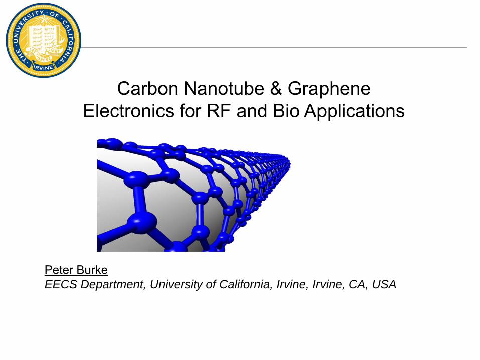
Allotropes of Carbon
A. Geim and K. Novoselov, "The Rise of Graphene", Nature Materials, 6, 183‐191, (2007).
2
AFFILIATION LOGO
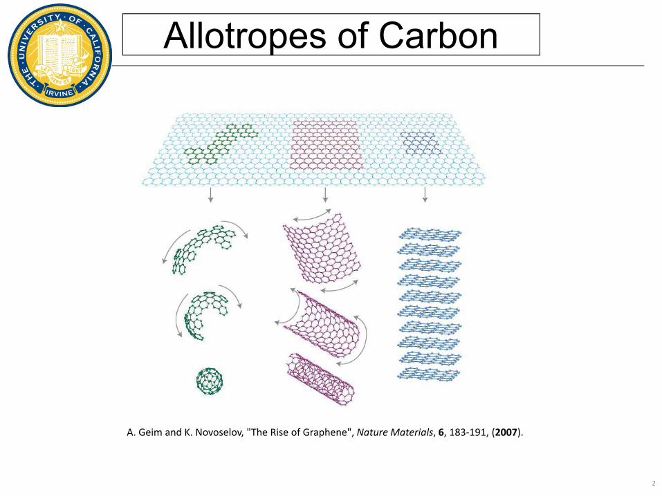
SWNT
L = 0.4 cmd = 1.5 nm
1 mm
Conductivity larger than copper!
AuAu
S. D. Li, Z. Yu, C. Rutherglen and P. J. Burke, "Electrical Properties of 0.4 Cm Long Single‐Walled Carbon Nanotubes", Nano Letters, 4, 2003‐2007, (2004).
d/L = cm/nm = 107
Would Schelkunoff be excited?
Single Walled Carbon Nanotube
3
AFFILIATION LOGO
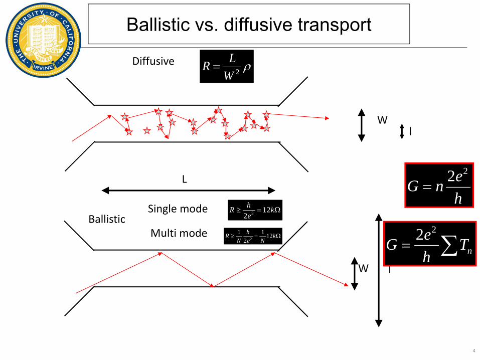
Ballistic vs. diffusive transport
2 122hR ke
≥ = Ω
21 1 12
2hR k
N e N≥ = Ω
W
W
l
l
L
Ballistic
Diffusive2
LRW
ρ=
Single mode
Multi mode
22eG nh
=
22n
eG Th
= ∑
4
AFFILIATION LOGO
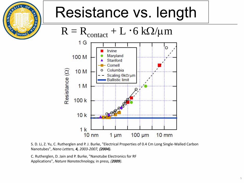
Resistance vs. lengthRcontact ≥ h/4e2 = 6 kΩR = Rcontact + L · 6 kΩ/μm
C. Rutherglen, D. Jain and P. Burke, "Nanotube Electronics for RF Applications", Nature Nanotechnology, in press, (2009).
5
S. D. Li, Z. Yu, C. Rutherglen and P. J. Burke, "Electrical Properties of 0.4 Cm Long Single‐Walled Carbon Nanotubes", Nano Letters, 4, 2003‐2007, (2004).
AFFILIATION LOGO
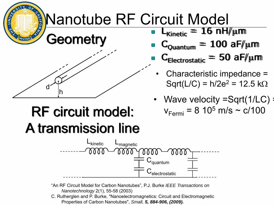
Nanotube RF Circuit Model
RF circuit model:A transmission line
Geometry
hd
Lkinetic Lmagnetic
Cquantum
Celectrostatic
“An RF Circuit Model for Carbon Nanotubes”, P.J. Burke IEEE Transactions on Nanotechnology 2(1), 55-58 (2003)
C. Rutherglen and P. Burke, "Nanoelectromagnetics: Circuit and Electromagnetic Properties of Carbon Nanotubes", Small, 5, 884-906, (2009).
2 25 CL hZ kC e
≡ = = Ω
1100
cVLC
≡ ≈
LKinetic = 16 nH/μmCQuantum = 100 aF/μm CElectrostatic = 50 aF/μm
• Characteristic impedance = Sqrt(L/C) = h/2e2 = 12.5 kΩ
• Wave velocity =Sqrt(1/LC) =vFermi = 8 105 m/s ~ c/100
AFFILIATION LOGO
--
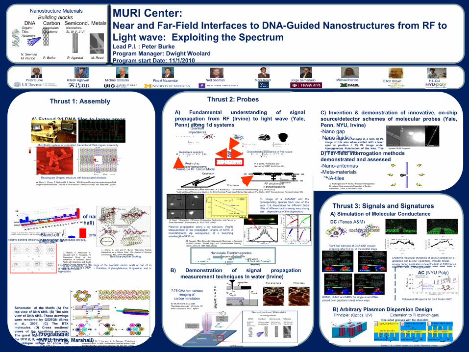
MURI Center: Near and Far-Field Interfaces to DNA-Guided Nanostructures from RF to Light wave: Exploiting the SpectrumLead P.I. : Peter BurkeProgram Manager: Dwight WoolardProgram start Date: 11/1/2010
Thrust 1: Assembly
A) Extend 2d DNA tiles to larger areas and 3d DNA tile assembly (Marshall and NYU)
B) Functionalization of nanostructures(NYU, Irvine, Marshall)-Antibodies for capture-Stand-off, remote electromagnetic interrogation
C) Programmable assembly of matter (NYU, Irvine, Marshall)-MURI focus on nanotubes/nanowiresS ifi i t ti
W. Shen, H. Zhong, D. Neff and M. L. Norton, “NTA Directed Protein Nanopatterning on DNA Origami Nanoconstructs", Journal of the American Chemical Society, 131, 6660-6661, (2009).
R. S. Wang, W. Y. Liu and N. C. Seeman, "PrototypingNanorod Control: A DNA Double Helix Sheathed within a DNASix-Helix Bundle", Chemistry & Biology, 16, 862-867, (2009).
Thrust 3: Signals and Signatures
Pendry, J. B., L. Martin-Moreno, et al. (2004). "Mimicking surface plasmons with structured surfaces." Science 305(5685): 847-848.
Principle: (Optics, UV) Extension to THz:(Michigan)B) Arbitrary Plasmon Dispersion Design
AC (NYU Poly)
DC (Texas A&M)
A) Simulation of Molecular Conductance
A) Fundamental understanding of signalpropagation from RF (Irvine) to light wave (Yale,Penn) along 1d systems
Thrust 2: Probes
B) Demonstration of signal propagationmeasurement techniques In water (Irvine)
STTR #W911NF-07-C-0098 “Nanotube Antennas” , UC Irvine, RF Nano Corporation, NIST, Agilent
RF-AFM tipSWNT
7.75 GHz non-contact imaging of
carbon nanotubes
D) Far-field interrogation methods demonstrated and assessed-Nano-antennas-Meta-materials-DNA-tiles
L. Zheng, D. Jain and P. Burke, "Nanotube Peptide Interactions on a Silicon Chip", The Journal of Physical Chemistry C, 113, 3978-3985, (2009).
Relative bonding efficiency of amino acids in to nanotubes and Sio2 . W= tryptophan.
C. Rajesh, C. Majumder, H.Mizuseki and Y. Kawazoe, "ATheoretical Study on theInteraction of Aromatic AminoAcids with Graphene and SingleWalled Carbon Nanotube", TheJournal of Chemical Physics,130, 124911, (2009).
L. Zheng, D. Jain and P. Burke, "Nanotube PeptideInteractions on a Silicon Chip", The Journal of PhysicalChemistry C, 113, 3978-3985, (2009).
Nanotube-peptide docking
RF vs. Quantum
Impedances
2 2 5 QhR k
e≡ = Ω 0
00
3 7 7 Z με
≡ = ΩResistance quantum Characteristic impedance of free space
0 121 3 7Q
ZR
α ≡ = ⋅
? ? ?d c
d c
VI
=
? ? ?R F
R F
VI
= ? ? ?R F
R F
EH
= ? ? ?o p t i c a l
o p t i c a l
EH
=
? ?
Realm of ac integrated nanosystems
P. J. Burke, "Nanotubes and Nanowires". 2007, World Scientific.
Nanoscale Electromagneticsconvergence in the THz
RF THz Light waveP. Burke UC
IrvineE. Brown
UCSBM. Reed, Yale- R. garwal, Pennfrequency
Rectangular Origami structure with biotinylated windows
Microfluidic system for controlled, hierarchical DNA origami assembly
Equilibrium geometry of the rings of the aromatic amino acids on top of a)graphene and b) 5,5 CNT : i Histidine, ii phenylalanine, iii tyrosine, and ivtryptophan.
Schematic of the Motifs (A) Thetop view of DNA 6HB. (B) The sideview of DNA 6HB. These drawingswere rendered by GIDEON (Biracet al., 2006). (C) The BTXmolecules. (D) Cross sectionalviews of the sheathing process.The guest duplex is connected tothe BTX (I, II, and III) molecule. (E)An oblique image to show thesheathing structure.
hd
Lkinetic Lmagnetic
CquantumCelectrostatic
Nanotube RF Circuit Model
RF circuit model:A transmission line
Geometry
“An RF Circuit Model for Carbon Nanotubes”, P.J. Burke IEEE Transactions on Nanotechnology 2(1), 55-58 (2003) “Luttinger Liquid Theory as a Model of the GHz Electrical Properties of Carbon Nanotubes”, P.J. Burke, IEEE Transactions on Nanotechnology 1(3),
129-144 (2002)
16 nH/mm
Plasmon propagation along a Ag nanowire. (Right)Measurement of the propagation lengths of SPPs inmicrofabricated Ag waveguides, at a launchingwavelength of 830 nm.
M. Reed, "Observation of Plasmon Propagation, Redirection, and Fan-out inSilver Nanowires", Nano Letters, 6, 1822-1826, (2006).
PL image of a ZnSeNW and thecorresponding spectra from one of theends. E-k dispersions for different ZnSeNWs of different radii showing very strongsize� dependence of the dispersions.
R. Agarwal, "Size-Dependent Waveguide Dispersion in NanowireOptical Cavities: Slowed Light and Dispersionless Guiding",Nano Letters, 9, 1684-1688, (2009).
One‐sided grooves with top dielectric
Calculated IR spectra for DNA Codon GGT
Front and sideview of DNA-CNT circular wrapping after 6.4 ns, at the middel stage of the process at 430 K
LAMMPS molecular dynamics of ssDNA junction on a) graphene and b) CNT electrodes. Van der Waals energy during application of electric field at 300K for c) DNA-CNT and d) DNA-graphene.
HOMO, LUMO and MEPs for single strand DNA placed over graphene sheet in four ways
MURI Proposal
C. Rutherglen and P. Burke, "Nanoelectromagnetics: Circuit and Electromagnetic Properties of Carbon Nanotubes", Small, 5, 884-906, (2009).
Agrawal, MURI Proposal
A) SEM image of a nanogap in a CdS. B) PLimage of this wire when excited with a laserspot at position I. C) PL image underhomogeneous illumination of the wire. Thiswire was cut at position V.
C) Invention & demonstration of innovative, on-chipsource/detector schemes of molecular probes (Yale,Penn, NYU, Irvine)-Nano gap-Nano fluidics
Nanostructure Materials
N. SeemanM. Norton
DNA Carbon Semicond. Metals
P. Burke R. Agarwal M. Reed
OrgamiTilesAptamers
NanotubesGraphene
Nanowires:Si, III-V, II-VI
Building blocks
Peter Burke Ned Seeman Michael NortonRitesh Agarwal Elliott BrownPinaki Mazumdar Mark ReedMichael Stroscio Jorge Semenario H.L.Cui
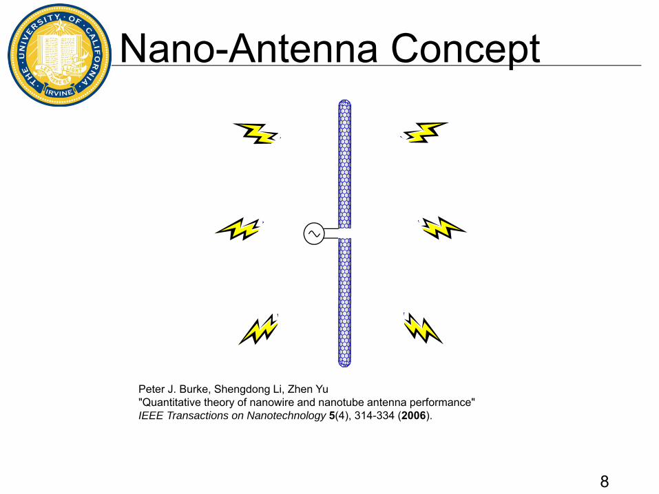
AFFILIATION LOGO Nano-Antenna Concept
Peter J. Burke, Shengdong Li, Zhen Yu"Quantitative theory of nanowire and nanotube antenna performance"IEEE Transactions on Nanotechnology 5(4), 314-334 (2006).
8
AFFILIATION LOGO
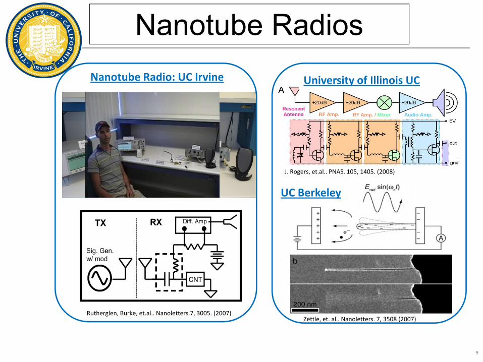
Nanotube Radio: UC Irvine
UC Berkeley
University of Illinois UC
Zettle, et. al.. Nanoletters. 7, 3508 (2007)
J. Rogers, et.al.. PNAS. 105, 1405. (2008)
Nanotube Radios
9
Rutherglen, Burke, et.al.. Nanoletters.7, 3005. (2007)
AFFILIATION LOGO
Press Coverage
Wilson Rothman. World’s Smallest Radio Is Just Atoms Wide, Still Needs AAA Battery (Oct. 18, 2007)
Barnaby Feder. Radio Nano Calling.. Testing 1,2,3,4 (Oct. 17, 2007)
‘World’s smallest radio’ unveiled (Oct. 18, 2007)
Alexis Madrigal. Nano Electronics Researcher Decodes Radio Signals Using Atom‐Sized Components(Oct. 17, 2007)
Jessica Thomas. Carbon nanotubes: Turn the radio up (if you can find it). Nature Nanotechnology 2, 744 (2007)
Micromini Radio. Science 9 November 2007: Vol. 318. no. 5852, p. 893
J. Scott Orr. Dust Gets Smart (Dec. 03, 2007)
10
AFFILIATION LOGO
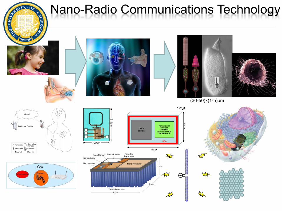
Nano-Radio Communications Technology
(30-50)x(1-5)um
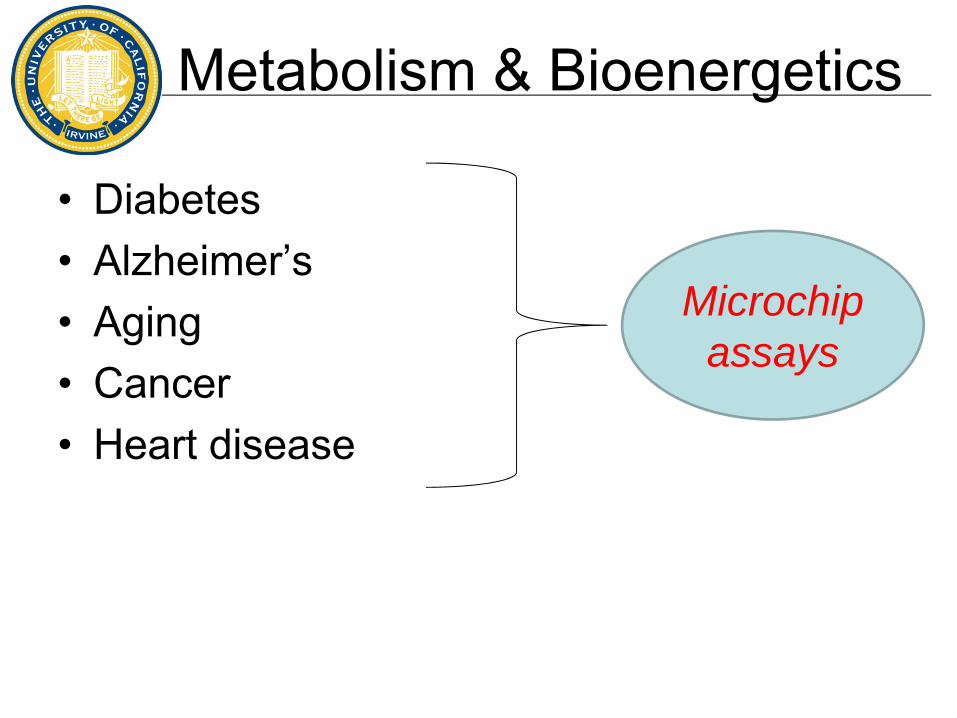
AFFILIATION LOGO Metabolism & Bioenergetics
• Diabetes• Alzheimer’s• Aging• Cancer• Heart disease
Microchip assays
AFFILIATION LOGO
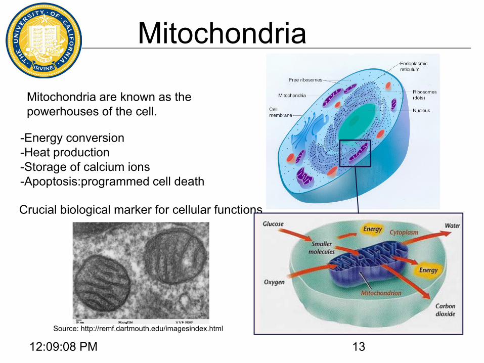
Mitochondria
12:09:08 PM 13Source: http://remf.dartmouth.edu/imagesindex.html
Crucial biological marker for cellular functions
-Energy conversion-Heat production-Storage of calcium ions-Apoptosis:programmed cell death
Mitochondria are known as the powerhouses of the cell.
AFFILIATION LOGO
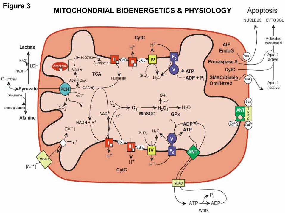
MITOCHONDRIAL BIOENERGETICS & PHYSIOLOGYFigure 3
AFFILIATION LOGO
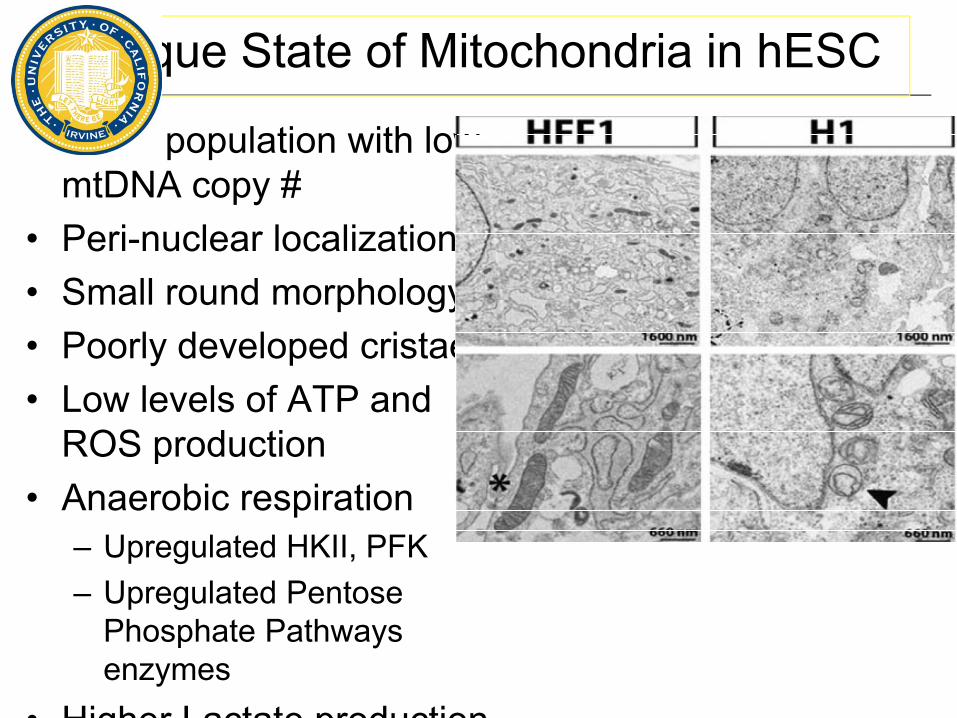
Unique State of Mitochondria in hESC
• Small population with low mtDNA copy #
• Peri-nuclear localization• Small round morphology• Poorly developed cristae• Low levels of ATP and
ROS production• Anaerobic respiration
– Upregulated HKII, PFK– Upregulated Pentose
Phosphate Pathways enzymes
• Higher Lactate production
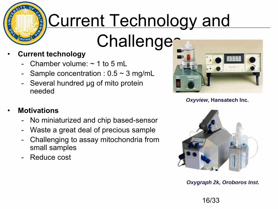
AFFILIATION LOGO Current Technology and
Challenges• Current technology
- Chamber volume: ~ 1 to 5 mL - Sample concentration : 0.5 ~ 3 mg/mL - Several hundred µg of mito protein
needed
• Motivations- No miniaturized and chip based-sensor - Waste a great deal of precious sample- Challenging to assay mitochondria from
small samples- Reduce cost
Oxyview, Hansatech Inc.
Oxygraph 2k, Oroboros Inst.
16/33
AFFILIATION LOGO
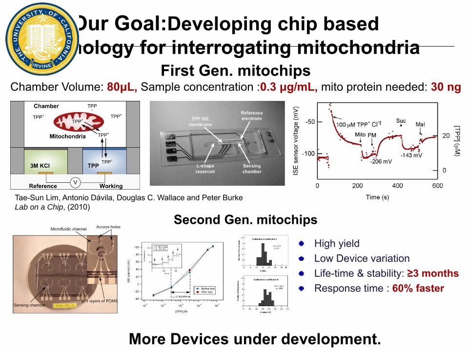
Our Goal:Developing chip based technology for interrogating mitochondria
Tae-Sun Lim, Antonio Dávila, Douglas C. Wallace and Peter BurkeLab on a Chip, (2010)
First Gen. mitochipsChamber Volume: 80μL, Sample concentration :0.3 μg/mL, mito protein needed: 30 ng
Second Gen. mitochips
More Devices under development.
High yield Low Device variationLife-time & stability: ≥3 monthsResponse time : 60% faster


![[ 25 ] (D. Huertas-Hernando, F. Guinea) Spin-Orbit Coupling in Curved Graphene, Fullerenes, Nanotubes, And Nanotube Caps](https://static.fdocuments.in/doc/165x107/577cdc6e1a28ab9e78aa8529/-25-d-huertas-hernando-f-guinea-spin-orbit-coupling-in-curved-graphene.jpg)