Basic Information of Operational Amplifiers Information of Operational Amplifiers Objectives of this...
51
Mr. V. VAITHIANATHAN, M.Tech (PhD) Assistant Professor, ECE Department EC1254 Linear Integrated Circuits Unit – I: Part - II Basic Information of Operational Amplifiers
Transcript of Basic Information of Operational Amplifiers Information of Operational Amplifiers Objectives of this...

Mr. V. VAITHIANATHAN, M.Tech (PhD)Assistant Professor, ECE Department
EC1254 Linear Integrated Circuits Unit – I: Part - II
Basic Information of Operational Amplifiers

Objectives of this presentation• To learn about
–Basic configuration of op-amp. –Packages of op-amp.–Power supply connections of op-amp.–Nomenclature of op-amp.–Characteristics of ideal operational
amplifier. –Characteristics of practical operational
amplifier.• Inverting Amplifier, Non-inverting Amplifier,
Voltage Follower, Differential Amplifier.

BASIC CONFIGURATION OF OPAMP• The op amp is one of the
basic building blocks of linear design.
• In its classic form it consists of – two input terminals, one
of which inverts the phase of the signal, the other preserves the phase and
– an output terminal.
• The standard symbol for the op amp is given in Figure.
• This ignores the power supply terminals, which are obviously required for operation.

PACKAGES OF OPAMP• There are three popular packages available:
– The metal can (TO) package– The dual-in-line package (DIP)– The flat package of flat pack
• Op-amp packages may contain single, two (dual) or four (quad) op-amps.
• Typical packages have 8 terminals (the can and the DIP or MINI DIP), 10 terminals (flatpacks and some cans) and 14 terminals (the DIP and the flat pack).

PACKAGES OF OPAMP• The widely used very popular type, for
example µA741 is a single op-amp and is available as an 8-pin can, an 8-pin DIP, a 10-pin flatpack or a 14-pin DIP.
• The µA741 is a dual 741 and comes in either a 10-pin can or a 14-pin DIP.
• Figure shows the various IC packages along with the top view of connection diagram.

PACKAGES OF OPAMPMetal can package (µA741)• The metal can has eight pins with pin number 8 identified by a tab. •The other pins are numbered counterclockwise from pin 8, beginning with pin 1. •Pin 2 is called the inverting input terminal •Pin 3 is the non-inverting input terminal•Pin 6 is the output terminal•Pins 7 and 4 are the power supply terminals labeled as V+ and V-respectively. •Terminals 1 and 5 are used for dc offset. •The pin 8 marked NC indicates 'No Connection'.

PACKAGES OF OPAMPDIP package of 741• The top pin on the left of the notch locates pin 1, and the flat pack ofhas a dot on it for identification. • The other pins are numbered counter-clockwise from pin 1.•The pin numbers have been illustrated only for some popular op-amps and the user should consult the manufacturer's data sheet before connecting a given op-amp into acircuit.

PACKAGES OF OPAMP

Power Supply Connections• The V+ and V- power supply terminals are
connected to two dc voltage sources. • The V+ pin is connected to the positive terminal of
one source and the V- pin is connected to the negative terminal of the other source as illustrated in figure (a) where the two sources are 15 V batteries each.
• These are typical values, but in general, the power supply voltage may range from about: ±5 V to ±22 V.
• The common terminal of the V+ and V- sources is connected to a reference point or ground.

Power Supply Connections
Power Supply Connections• Some op-amps have a ground terminal, but most
do not. The ground is simply a convenient point on the circuit bread-board to which the op-amp is connected through the power supplies.
• The equivalent representation of fig. (a) is given in fig. (b).
• The common point of the two supplies must be grounded, otherwise twice the supply voltage will get applied and it may damage the op-amp.
• Instead of using two power supplies, one can use a single power supply to obtain V+ and V- as shown in circuits of fig. (c, d, e).

Power Supply Connections

Power Supply Connections• In fig. (c), resistor R should be greater than 10 kΩ
so that it does not draw more current from the supply Vs.
• The two capacitors provide decoupling of the power supply and range in value from 0.01 to 10µF.
• In the circuit of fig. (d), zener diodes are used to give symmetrical supply voltages.
• The value of the resistor Rs is chosen such that it supplies sufficient current for the zener diodes to operate in the avalanche mode.

Power Supply Connections• In fig. (e), potentiometer is used to get equal
values of V+ and V- .
• Diodes D1 and D2 protect the IC if the positive and negative leads of the supply voltage Vs are accidentally reversed.
• These diodes can also be connected in the circuits of fig. (c) and (d).

Manufacturer's Designation• Each manufacturer uses a specific code and
assigns a specific type number to the ICs produced.
• For example, 741 an internally compensated op-amp originally manufactured by Fairchild is sold as µA741.
• Here µA represents the identifying initials used by Fairchild.

Manufacturer's Designation• The codes used by some of the well-known
manufacturers of linear ICs are:
– Fairchild - µA, µAF
– National Semiconductor - LM, LH, LF, TBA
– Motorola - MC, MFC
– RCA - CA, CD
– Texas Instruments - SN
– Signetics - N/S, NE/SE
– Burr-Brown - BB

Manufacturer's Designation• A number of manufacturers also produce popular
ICs of the other manufacturers. • For easy use, they usually retain the original type
number of the IC along with their identifying initials.
• For example, Fairchild's original µA741 is also manufactured by other manufacturers as follows:– National Semiconductor - LM741– Motorola - MC1741– RCA - CA3741– Texas Instruments - SN52741– Signetics - N5741

Manufacturer's Designation• It may be noted that the last three digits in each
manufacturer's designation are 741.• All these op-amps have the same specifications.
Since a number of manufacturers produce the same IC, one can refer to such ICs by their type number only and delete manufacturer's identifying initials.
• For example, µ741 or MC1741 may simple be referred as 741.
• Some linear ICs are available in different classes such as A, C, E, Sand SC.

Manufacturer's Designation• For example 741, 741 A, 741C, 741 E, 741 Sand
741 SC are different versions of the same op-amp.• The main difference of these op-amps are:
– 741 :Military grade op-amp (Operating temperature range -55° to 125°C)
– 741C :Commercial grade op-amp (Operating temperate range 0° to 700/75°C)
– 741A :Improved version of 741 Better electrical specifications
– 741E :Improved version of 741 C - Better electrical specifications
– 741S :Military grade op-amp with higher slew-rate– 741SC :Commercial grade op-amp with higher slew-
rate

Ideal Operational Amplifier• The schematic symbol of an op-amp is shown in
fig. (a).
• It has two input terminals and one output terminal.
• Other terminals have not been shown for simplicity.
• The - and + symbols at the input refer to inverting and non-inverting input terminals respectively.

Ideal Operational Amplifier• If V1 = 0, output Vo is 180° out of phase with
input signal V2. When V2 = 0, output Vo will be in phase with the input signal applied at V1.
• This op-amp is said to be ideal if it has the following characteristics.
– Open loop voltage gain : AOL = ∞
– Input impedance : Ri = ∞
– Output impedance :Ro = 0
– Bandwidth : BW = ∞
– Zero offset : Vo when V1 = V2 = 0

Ideal Operational Amplifier• An ideal op-amp draws no current at both the input
terminals i.e., i1 =i2 =0. • Because of infinite input impedance, any signal
source can drive it and there is no loading on the preceding driver stage.
• Since gain is ∞, the voltage between the inverting and non-inverting terminals, i.e., differential input voltage Vd=(V1 – V2) is essentially zero for finite output voltage Vo.
• The output voltage Vo is independent of the current drawn from the output as Ro = 0.
• The output thus can drive an infinite number of other devices.

Ideal Operational Amplifier• An ideal op-amp draws no current at both the
input terminals i.e., i1 =i2 =0. • Because of infinite input impedance, any signal
source can drive it and there is no loading on the preceding driver stage.
• Since gain is ∞, the voltage between the inverting and non-inverting terminals, i.e., differential input voltage Vd=(V1 – V2) is essentially zero for finite output voltage Vo.
• The output voltage Vo is independent of the current drawn from the output as Ro = 0.

Ideal Operational Amplifier• The output thus can drive an infinite number of
other devices.
• A physical amplifier is not an ideal one. So, the equivalent circuit of an op-amp may be shown in fig. (b) where AOL ‡ ∞, Ri ‡ ∞ and RO = 0.

Ideal Operational Amplifier• It can be seen that op-amp is a voltage controlled
voltage source and AOL· Vd is an equivalent Theveninvoltage source and Ro is the Thevenin equivalent resistance looking back into the output terminal of an op-amp.
• The equivalent circuit is useful in analyzing the basic operating principles of op-amp.
• For the circuit shown in fig. (b), VO is
• The equation shows that the op-amp amplifies the difference between the two input voltages.

Open Loop Operation - OpAmp• The simplest way to use an op-amp is in the open
loop mode. • Refer to fig. (c) where signals V1 and V2 are applied
at non-inverting and inverting input terminals respectively.

Feedback in Ideal Op-Amp• The utility of an op-amp can be greatly increased by
providing negative feedback. The output in this case is not driven into saturation and the circuit behaves in a linear manner.
• There are two basic feedback connections used. In order to understand the operation of these circuits, we make two realistic simplifying assumptions discussed earlier also.– The current drawn by either of the input
terminals (non-inverting and inverting) is negligible.
– The differential input voltage Vd between non-inverting and inverting input terminals is essentially zero.

Inverting Amplifier• This is perhaps the most widely used of all the op-
amp circuits. • The output voltage Vo is fed back to the inverting
input terminal through the Rf –R1 network where Rfis the feedback resistor.
• Input signal Vi (ac or dc) is applied to the inverting input terminal through R1 and non-inverting input terminal of op-amp is grounded.
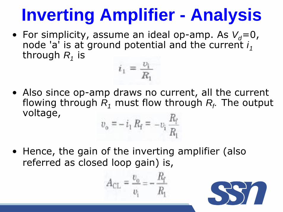
Inverting Amplifier - Analysis• For simplicity, assume an ideal op-amp. As Vd=0,
node 'a' is at ground potential and the current i1through R1 is
• Also since op-amp draws no current, all the current flowing through R1 must flow through Rf. The output voltage,
• Hence, the gain of the inverting amplifier (also referred as closed loop gain) is,

Inverting Amplifier - Analysis• Alternatively, the nodal equation at the node 'a' in
fig. is
where va is the voltage at node 'a'. Since node 'a' is at virtual ground va = O. Therefore, we get,
• The negative sign indicates a phase shift of 180°between Vi and Vo.
• Also since inverting input terminal is at virtual ground, the effective input impedance is R1

Inverting Amplifier - Analysis• The value of R1 should be kept fairly large to avoid
loading effect.• This however, limits the gain that can be obtained
from this circuit. • A load resistor RL is usually put at the output in
actual practice otherwise, the input impedance of the measuring device such as oscilloscope or DVM acts as the load.
• If, however, resistances R1 and Rf in Fig. 2.5 (a) are replaced by impedances Z1 and Zf respectively, then the voltage gain, ACL will be
• This expression for the voltage gain will be used in op-amp application, such as integrator, differentiator etc.

Practical Inverting Amplifier• For a practical op-amp, the expression for the
closed loop voltage gain should be calculated using the low frequency model. The equivalent circuit of a practical inverting amplifier is shown in fig. (a)

Practical Inverting Amplifier• This circuit can be simplified by replacing the signal
source Vi and resistors R1 and Ri by Thevenin's equivalent as shown in fig. (b) which is analyzed to calculate the exact expression for closed loop gain, ACL and input impedance Rif.

Practical Inverting Amplifier• The input impedance Ri of an op-amp is usually
much greater than R1, so one may assume, Veq =Viand Req=R1.From the output loop in fig. (b)
• Putting the value of Vd and simplifying,
• Also the KVL loop equation gives

Practical Inverting Amplifier• Putting the value of i from and solving for closed
loop gain ACL = Vo/Vi
• if AOL » 1 and AOLR1 » Ro + Rf, and neglecting Ro,
• Input Resistance Rf– Writing the loop equation and solving for Rif,

Practical Inverting Amplifier• Output Resistance Rof
• Output impedance Rof (without load resistance RL is calculated from the open circuit output voltage vocand short circuit output circuit isc.
• Now consider the circuit shown in Fig. (c).

Practical Inverting Amplifier• Under short circuit conditions at output,

Practical Inverting Amplifier
• Putting the value of ACL
• It may be seen that numerator consists of a term Ro||(R1+Rf) and is therefore smaller than Ro.
• The output resistance Rof (with feedback) is therefore always less than Ro and
for ACL ≈ ∞, Rof≈ 0.

Non Inverting Amplifier• If a signal (ac or dc) is applied to the non-inverting
input terminal and feedback is given as shown in fig. (a), the circuit amplifies without inverting the input signal.
• Such a circuit is called non-inverting amplifier.

Non Inverting Amplifier• It may be noted that it is also a negative feed-back
system as output is being fed back to the inverting input terminal.
• As the differential voltage Vd at the input terminal of op-amp is zero, the voltage at node 'a' in fig. (a) is Vi same as the input voltage applied to non-inverting input terminal.
• Now Rf and R1 forms a potential divider. Hence
as no current flows into the op-amp.

Non Inverting Amplifier• Thus, for non-inverting amplifier the voltage gain,
• The gain can be adjusted to unity or more, by proper selection of resistors Rf and R1.
• Compared to the inverting amplifier, the input resistance of the non-inverting amplifier is extremely large (= ∞) as the op-amp draws negligible current from the signal source.

Non Inverting Amplifier• The analysis of a practical non-inverting amplifier
can be performed by using the equivalent circuit shown in fig. (b).

Non Inverting Amplifier• Writing KCL at the output node,

Voltage Follower• In the non-inverting amplifier of fig. if Rf =0 and
R1=∞, we get the modified circuit.

Differential Amplifier• A circuit that amplifies the difference between two
signals is called a difference or differential amplifier. • This type of the amplifier is very useful in
instrumentation circuits • A typical circuit is shown in fig.

Differential Amplifier• Since, the differential voltage at the input terminals
of the op-amp is zero, nodes 'a' and 'b' are at the same potential, designated as V3.
• The nodal equation at 'a' is,
• The nodal equation at ‘b' is,

Differential AmplifierDifference-mode and Common-mode Gains
• if V1 =V2 then Vo= 0. That is, the signal common to both inputs gets cancelled and produces no output voltage.
• This is true for an ideal op-amp, however, a practical op-amp exhibits some small response to the common mode component of the input voltages too.
• The output voltage depends not only upon the difference signal Vd at the input, but is also affected by the average voltage of the input signals, called the common-mode signal VCM.

Differential AmplifierDifference-mode and Common-mode Gains
• The common-mode signal VCM. defined as,
• For differential amplifier, though the circuit is symmetric, but because of the mismatch, the gain at the output with respect to the positive terminal is slightly different in magnitude to that of the negative terminal.
• So, even with the same voltage applied to both inputs, the output is not zero.
• The output, therefore, must be expressed as,

Differential AmplifierDifference-mode and Common-mode Gains
• The output, therefore, must be expressed as,
where, A1(A2) is the voltage amplification from input 1 (2) to the output with input 2(1) grounded.

Differential AmplifierCommon-Mode Rejection Ratio
• The relative sensitivity of an op-amp to a difference signal as compared to a common-mode signal is called common-mode rejection ratio (CMRR) and gives the figure of merit ρ for the differential amplifier.
• So, CMRR is given by:
• It is usually expressed in decibels (dB).
• For example, the µA741 op-amp has a minimum CMRR of 70 dB whereas a precision op-amp such as µA725A has a minimum CMRR of 120 dB.

Conclusion • In this presentation, we learnt about
–Basic configuration of op-amp. –Packages of op-amp.–Power supply connections of op-amp.–Nomenclature of op-amp.–Characteristics of ideal operational
amplifier. –Characteristics of practical operational
amplifier.