Basic Bit Memory: Latches and Flip Flops - Edward … Bit Memory: Latches and Flip ... We consider a...
32
CPSC 2105 Revised 5/14/2013 Page 1 of 32 Basic Bit Memory: Latches and Flip–Flops Topics: 1. General description of bit memory, also called a memory cell. 2. Definition of sequential and combinational circuits. Memory devices are sequential devices. 3. Discussion of the CPU system clock. 4. Functional description of latches and flip–flops. The four basic types: SR, JK, D, and T. 5. Characterizations of latches and flip–flops. 6. The CPU clock and loading a D latch or flip–flop.
-
Upload
truonghanh -
Category
Documents
-
view
218 -
download
1
Transcript of Basic Bit Memory: Latches and Flip Flops - Edward … Bit Memory: Latches and Flip ... We consider a...

CPSC 2105 Revised 5/14/2013 Page 1 of 32
Basic Bit Memory:
Latches and Flip–Flops
Topics:
1. General description of bit memory, also called a memory cell.
2. Definition of sequential and combinational circuits.
Memory devices are sequential devices.
3. Discussion of the CPU system clock.
4. Functional description of latches and flip–flops.
The four basic types: SR, JK, D, and T.
5. Characterizations of latches and flip–flops.
6. The CPU clock and loading a D latch or flip–flop.
Digital Memory: Latches and Flip-Flops
CPSC 2105 Revised 5/14/2013 Page 2 of 32
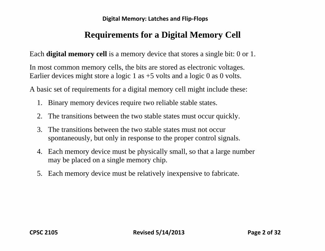
Requirements for a Digital Memory Cell
Each digital memory cell is a memory device that stores a single bit: 0 or 1.
In most common memory cells, the bits are stored as electronic voltages.
Earlier devices might store a logic 1 as +5 volts and a logic 0 as 0 volts.
A basic set of requirements for a digital memory cell might include these:
1. Binary memory devices require two reliable stable states.
2. The transitions between the two stable states must occur quickly.
3. The transitions between the two stable states must not occur
spontaneously, but only in response to the proper control signals.
4. Each memory device must be physically small, so that a large number
may be placed on a single memory chip.
5. Each memory device must be relatively inexpensive to fabricate.
Digital Memory: Latches and Flip-Flops
CPSC 2105 Revised 5/14/2013 Page 3 of 32
Sequential Circuits
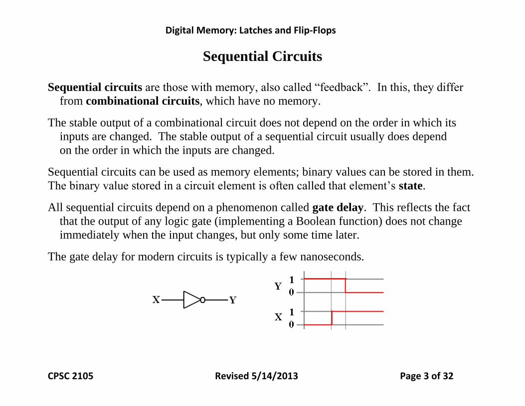
Sequential circuits are those with memory, also called “feedback”. In this, they differ
from combinational circuits, which have no memory.
The stable output of a combinational circuit does not depend on the order in which its
inputs are changed. The stable output of a sequential circuit usually does depend
on the order in which the inputs are changed.
Sequential circuits can be used as memory elements; binary values can be stored in them.
The binary value stored in a circuit element is often called that element’s state.
All sequential circuits depend on a phenomenon called gate delay. This reflects the fact
that the output of any logic gate (implementing a Boolean function) does not change
immediately when the input changes, but only some time later.
The gate delay for modern circuits is typically a few nanoseconds.

Digital Memory: Latches and Flip-Flops
CPSC 2105 Revised 5/14/2013 Page 4 of 32
Synchronous Sequential Circuits
We usually focus on clocked sequential circuits,
also called synchronous sequential circuits.
As the name “synchronous” implies, these circuits respond to a system clock,
which is used to synchronize the state changes of the various sequential circuits.
The main function of a system clock is the coordination of events in different circuits
in the computer. One can design asynchronous sequential circuits, which are not
controlled by a system clock. They present significant design challenges related to
timing issues, and are so complex that they are considered not to be reliable.
The system clock is a circuit that emits a sequence of regular pulses with a fixed and
reliable pulse rate. If you have an electronic watch (who doesn’t?), what you have is
a small electronic circuit emitting pulses and a counter circuit to count them.
Clock frequencies are measured in
kilohertz thousands of ticks per second
megahertz millions of ticks per second
gigahertz billions of ticks per second.

Digital Memory: Latches and Flip-Flops
CPSC 2105 Revised 5/14/2013 Page 5 of 32
Views of the System Clock
There are a number of ways to view the system clock. In general, the view depends on
the detail that we need in discussing the problem. The logical view is shown in the next
figure, which illustrates some of the terms commonly used for a clock.
The clock is typical of a periodic function. There is a period for which f(t) = f(t + )
The rising edge is often called the “leading edge”.
The falling edge is often called the “trailing edge”.
NOTATION: We always call the present clock tick “t” and the next one “t + 1”.
All we are doing is counting the clock ticks.

Digital Memory: Latches and Flip-Flops
CPSC 2105 Revised 5/14/2013 Page 6 of 32
Views of the System Clock
The top view is the “real physical view”. It is seldom used.
The middle view reflects the fact that voltage levels do not change instantaneously.
We use this view when considering system busses.
Digital Memory: Latches and Flip-Flops
CPSC 2105 Revised 5/14/2013 Page 7 of 32
Clock Period and Frequency
If the clock period is denoted by , then the frequency (by definition) is f = 1 / .
For example, if = 2.0 nanoseconds, also written as = 2.010–9 seconds, then
f = 1 / (2.010–9 seconds) = 0.50109 seconds–1 or 500 megahertz.
If f = 2.5 Gigahertz, also written as 2.5109 seconds–1, then
= 1.0 / (2.5109 seconds–1) = 0.410–9 seconds = 0.4 nanosecond.

Digital Memory: Latches and Flip-Flops
CPSC 2105 Revised 5/14/2013 Page 8 of 32
Latches and Flip–Flops: First Definition
We consider a latch or a flip–flop as a device that stores a single binary value.
Flip–flops and clocked latches are devices that accept input at fixed times dictated by
the system clock. For this reason they are called “synchronous sequential circuits”.
Denote the present time by the symbol t. Denote the clock period by .
Rather than directly discussing the clock period, we merely say that
the current time is t
after the next clock tick the time is (t + 1)
The present state of the device is often called Q(t)
The next state of the device is often called Q(t + 1)
The sequence: the present state is Q(t), the clock “ticks”, the state is now Q(t + 1)
AGAIN: We call the next state Q(t + 1), even if the transition from Q(t) to
Q(t + 1) takes only a few nanoseconds. We are counting the actual
number of clock ticks, not the amount of time they take.

Digital Memory: Latches and Flip-Flops
CPSC 2105 Revised 5/14/2013 Page 9 of 32
Latches and Flip–Flops: When Triggered
Clocked latches accept input when the system clock is at logic high.
Flip–flops accept input on either the rising edge of the system clock.
Digital Memory: Latches and Flip-Flops
CPSC 2105 Revised 5/14/2013 Page 10 of 32
Advantages of Flip–Flops
When either a flip–flop or a latch is used as a part of a circuit, we have the problem
of feedback. In this, the output of the device is processed and then used as input.
Example: The flip–flop is a part of a register that is to be incremented.
We define the data path for the computer as following the output of the flip–flop
through the processing elements and back to the input of the flip–flop.
The data path time is the amount of time that it takes the data to travel the data path.
If this time is too short, the processed output of the flip–flop can get back to its input
during the time when the flip–flop remains sensitive to its input.
A flip–flop is a latch that has been modified to minimize the time during which the
device responds to its input.
This minimizes the possibility of uncontrolled feedback as associated instabilities.
Digital Memory: Latches and Flip-Flops
CPSC 2105 Revised 5/14/2013 Page 11 of 32
Describing Flip–Flops
A flip–flop is a “bit bucket”; it holds a single binary bit.
A flip–flop is characterized by its current state: Q(t).
We want a way to describe the operation of the flip–flops.
How do these devices respond to the input? We use tables to describe the operation.
Characteristic tables: Given Q(t), the present state of the flip–flop, and
the input, what will Q(t + 1), the next state of the flip–flop, be?
Excitation tables: Given Q(t), the present state of the flip–flop, and
Q(t + 1), the desired next state of the flip–flop,
what input is required to achieve that change.

Digital Memory: Latches and Flip-Flops
CPSC 2105 Revised 5/14/2013 Page 12 of 32
Functional Definition of Flip–Flops
We use the characteristic table to describe both latches and flip–flops.
The characteristic table takes the present state and input and shows the next state.
Here is the characteristic table for an SR flip–flop.
S R Present State Next State
0 0 0 0
0 0 1 1
0 1 0 0
0 1 1 0
1 0 0 1
1 0 1 1
1 1 0 ERROR
1 1 1 ERROR

Digital Memory: Latches and Flip-Flops
CPSC 2105 Revised 5/14/2013 Page 13 of 32
Characteristic Tables
We often take a table such as
S R Present State Next State
0 0 0 0
0 0 1 1
0 1 0 0
0 1 1 0
1 0 0 1
1 0 1 1
1 1 0 ERROR
1 1 1 ERROR
And abbreviate it as
S R Q(t + 1) = Next State
0 0 Q(t)
0 1 0
1 0 1
1 1 ERROR
Digital Memory: Latches and Flip-Flops
CPSC 2105 Revised 5/14/2013 Page 14 of 32
Comment on Notation Used
All flip–flops have a number of inputs that your instructor does not indicate unless
they are required for discussion of the circuit.
Power every flip–flop must be powered
Ground every flip–flop must be grounded
Clock all flip–flops are clocked devices
Asynchronous Clear this allows the flip–flop to be cleared independently of the
clock. In other words, make Q(t) = 0.
Asynchronous Set this allows the flip–flop to be set independently of the
clock. In other words, make Q(t) = 1.
Absent the explicit clock input, your instructor’s circuits might resemble unclocked
latches. Your instructor does not use such latches, but designs only with flip–flops.

Digital Memory: Latches and Flip-Flops
CPSC 2105 Revised 5/14/2013 Page 15 of 32
SR Flip–Flop
We now adopt a functional view. How does the next state depend on the present
state and input. A flip–flop is a “bit holder”.
Here is the diagram for the SR flip–flop.
Here again is the state table for the SR flip–flop.
S R Q(t + 1)
0 0 Q(T)
0 1 0
1 0 1
1 1 ERROR
Note that setting both S = 1 and R = 1 causes the flip–flop to enter a logically
inconsistent state, followed by an unpredictable, almost random, state. For this reason,
we label the output for S = 1 and R = 1 as an error.

Digital Memory: Latches and Flip-Flops
CPSC 2105 Revised 5/14/2013 Page 16 of 32
We Need Another Flip–Flop
Consider the characteristic table for the SR flip–flop.
It is the same as that for the SR latch, except for the explicit reference to the clock.
S R Q(t + 1)
0 0 Q(t)
0 1 0
1 0 1
1 1 ERROR
Were we to modify the SR flip–flop, what could be placed in the last row?
It is easy to see that there are only four Boolean functions of a single Boolean variable Q.
F(Q) = 0, F(Q) = Q, F(Q) = Q , and F(Q) = 1. The above table is missing Q .
This gives rise to the JK, the most general of the flip–flops. Its characteristic table is:
J K Q(t + 1)
0 0 Q(t)
0 1 0
1 0 1
1 1 tQ

Digital Memory: Latches and Flip-Flops
CPSC 2105 Revised 5/14/2013 Page 17 of 32
JK Flip–Flop
A JK flip–flop generalizes the SR to allow for both inputs to be 1.
Here is the characteristic table for a JK flip–flop.
J K Q(t + 1)
0 0 Q(t)
0 1 0
1 0 1
1 1 tQ Note that the flip–flop can generate all four possible functions of a single variable:
the two constants 0 and 1
the variables Q and Q .

Digital Memory: Latches and Flip-Flops
CPSC 2105 Revised 5/14/2013 Page 18 of 32
The D Flip–Flop
The D flip–flop specializes either the SR or JK to store a single bit. It is very useful for
interfacing the CPU to external devices, where the CPU sends a brief pulse to set the
value in the device and it remains set until the next CPU signal.
The characteristic table for the D flip–flop is so simple that it is expressed better as the
equation Q(t + 1) = D. Here is the table.
D Q(t + 1)
0 0
1 1

Digital Memory: Latches and Flip-Flops
CPSC 2105 Revised 5/14/2013 Page 19 of 32
The T Flip–Flop
The “toggle” flip–flop allows one to change the value stored. It is often used in circuits
in which the value of the bit changes between 0 and 1, as in a modulo–4 counter in which
the low–order bit goes 0, 1, 0, 1, 0, 1, etc.
The characteristic table for the D flip–flop is so simple that it is expressed better as the
equation Q(t + 1) = Q(t) T. Here is the table.
T Q(t + 1)
0 Q(t)
1 tQ
Here the symbol “T” denotes the input; “t” and “t + 1” denote time.
Digital Memory: Latches and Flip-Flops
CPSC 2105 Revised 5/14/2013 Page 20 of 32
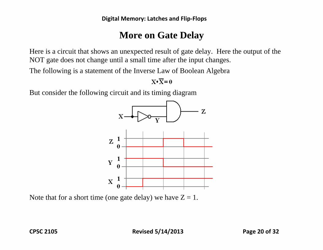
More on Gate Delay
Here is a circuit that shows an unexpected result of gate delay. Here the output of the
NOT gate does not change until a small time after the input changes.
The following is a statement of the Inverse Law of Boolean Algebra
But consider the following circuit and its timing diagram
Note that for a short time (one gate delay) we have Z = 1.

Digital Memory: Latches and Flip-Flops
CPSC 2105 Revised 5/14/2013 Page 21 of 32
A NOR Gate with Feedback
We consider yet another circuit that is based on gate delays.
This is based on the NOR gate, which is an OR gate followed by a NOT gate.
Now consider the truth table for the NOR gate, which we build from the truth tables for
the OR gate and the NOT gate.
X Y W Z
0 0 0 1
0 1 1 0
1 0 1 0
1 1 1 0
The important thing to note is can be expressed in two equations.

Digital Memory: Latches and Flip-Flops
CPSC 2105 Revised 5/14/2013 Page 22 of 32
A NOR Gate with Feedback (Part 2)
Consider the following circuit. When X = 1, Z = 0, and Y = 0. It is stable.
The reason for stability is the property of the NOR gate when X = 1.
In particular, for Z = 0, we have Y = 0, and
Thus, Z does not change and Y does not change; provided only that X does not change.
Digital Memory: Latches and Flip-Flops
CPSC 2105 Revised 5/14/2013 Page 23 of 32
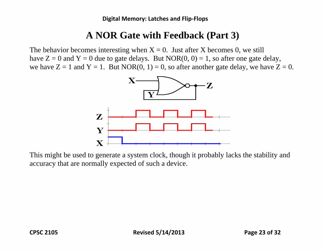
A NOR Gate with Feedback (Part 3)
The behavior becomes interesting when X = 0. Just after X becomes 0, we still
have Z = 0 and Y = 0 due to gate delays. But NOR(0, 0) = 1, so after one gate delay,
we have Z = 1 and Y = 1. But NOR(0, 1) = 0, so after another gate delay, we have Z = 0.
This might be used to generate a system clock, though it probably lacks the stability and
accuracy that are normally expected of such a device.

Digital Memory: Latches and Flip-Flops
CPSC 2105 Revised 5/14/2013 Page 24 of 32
Cross–Coupled NOR Gates: The SR Latch
Consider the following circuit. Each of the two NOR gates has two inputs, one from an
external source and one that is fed back from the other NOR gate.
Here the two external inputs are 0 and 0. We do not specify the outputs, except to require
that one is the complement of the other; if Q = 1, then Q = 0, and vice versa.
The two inputs to the top NOR gate are 0 and Q. But
so this part of the circuit is stable.
The two inputs to the bottom NOR gate are 0 and Q . But
so this part of the circuit is also stable.
The circuit is stable with external inputs of 0 and 0.

Digital Memory: Latches and Flip-Flops
CPSC 2105 Revised 5/14/2013 Page 25 of 32
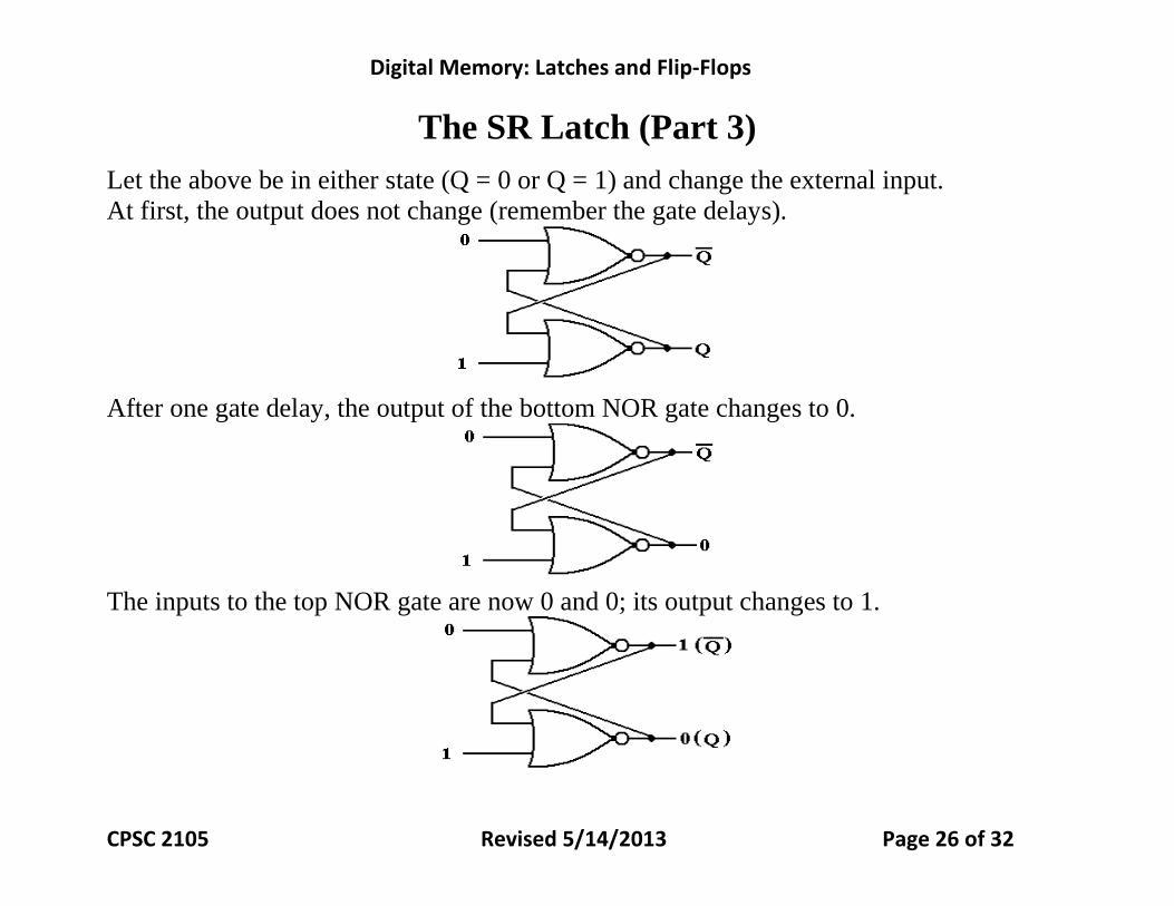
The SR Latch (Part 2)
Let the above be in either state (Q = 0 or Q = 1) and change the external input.
At first, the output does not change (remember the gate delays).
After one gate delay, the output of the top NOR gate changes to 0.
The inputs to the bottom NOR gate are now 0 and 0. After another gate delay it changes.
Digital Memory: Latches and Flip-Flops
CPSC 2105 Revised 5/14/2013 Page 26 of 32
The SR Latch (Part 3)
Let the above be in either state (Q = 0 or Q = 1) and change the external input.
At first, the output does not change (remember the gate delays).
After one gate delay, the output of the bottom NOR gate changes to 0.
The inputs to the top NOR gate are now 0 and 0; its output changes to 1.

Digital Memory: Latches and Flip-Flops
CPSC 2105 Revised 5/14/2013 Page 27 of 32
The SR Latch (Part 4)
We now have a basic memory device, which stores one bit denoted as Q.
Here is the general circuit diagram of the device.
So, we have a device that can store a single bit, with the following options:
1. Store a 0
2. Store a 1
3. Retain the current contents.
The behavior of such a memory device is described by its characteristic table.
Digital Memory: Latches and Flip-Flops
CPSC 2105 Revised 5/14/2013 Page 28 of 32
The SR Latch (Part 5)
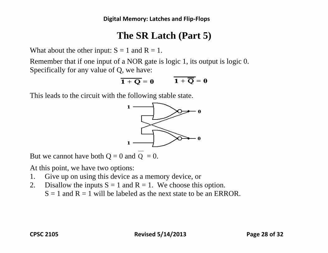
What about the other input: S = 1 and R = 1.
Remember that if one input of a NOR gate is logic 1, its output is logic 0.
Specifically for any value of Q, we have:
This leads to the circuit with the following stable state.
But we cannot have both Q = 0 and Q = 0.
At this point, we have two options:
1. Give up on using this device as a memory device, or
2. Disallow the inputs S = 1 and R = 1. We choose this option.
S = 1 and R = 1 will be labeled as the next state to be an ERROR.
Digital Memory: Latches and Flip-Flops
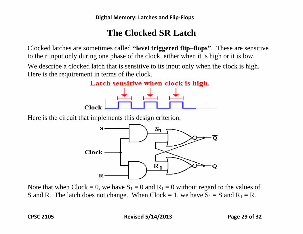
CPSC 2105 Revised 5/14/2013 Page 29 of 32
The Clocked SR Latch
Clocked latches are sometimes called “level triggered flip–flops”. These are sensitive
to their input only during one phase of the clock, either when it is high or it is low.
We describe a clocked latch that is sensitive to its input only when the clock is high.
Here is the requirement in terms of the clock.
Here is the circuit that implements this design criterion.
Note that when Clock = 0, we have S1 = 0 and R1 = 0 without regard to the values of
S and R. The latch does not change. When Clock = 1, we have S1 = S and R1 = R.
Digital Memory: Latches and Flip-Flops
CPSC 2105 Revised 5/14/2013 Page 30 of 32
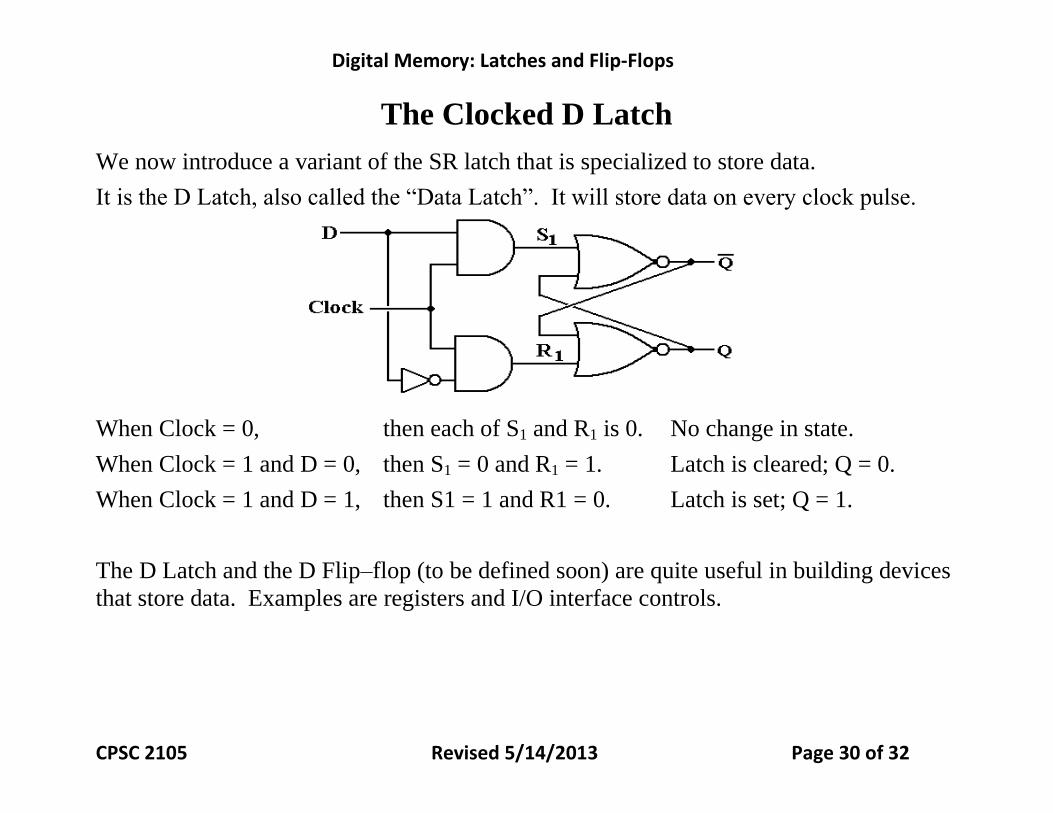
The Clocked D Latch
We now introduce a variant of the SR latch that is specialized to store data.
It is the D Latch, also called the “Data Latch”. It will store data on every clock pulse.
When Clock = 0, then each of S1 and R1 is 0. No change in state.
When Clock = 1 and D = 0, then S1 = 0 and R1 = 1. Latch is cleared; Q = 0.
When Clock = 1 and D = 1, then S1 = 1 and R1 = 0. Latch is set; Q = 1.
The D Latch and the D Flip–flop (to be defined soon) are quite useful in building devices
that store data. Examples are registers and I/O interface controls.

Digital Memory: Latches and Flip-Flops
CPSC 2105 Revised 5/14/2013 Page 31 of 32
Remember the Pulse Generator?
The problem with the clocked latch is that it is sensitive to its input for an excessive
amount of time. This can lead to instabilities in the circuitry.
We need to devise a circuit that will give a very short pulse, resembling a clock pulse,
but only on the rising edge of the system clock. We have such a circuit.

Digital Memory: Latches and Flip-Flops
CPSC 2105 Revised 5/14/2013 Page 32 of 32
The SR and D Flip–Flops
Here is the circuit diagram for an SR flip–flop that is fabricated from NOR gates.
One can also fabricate it from NAND gates, but we ignore this option.
Here is the circuit diagram for a D flip–flop that is fabricated from NOR gates.